Article

Design and Implementation of Self-Limiting Two-Stage LC Oscillators Using Cascade Structure of Monolithic CCIIs as Active Elements

Faculty of Electronic Engineering and Technologies, Technical University of Sofia, 1000 Sofia, Bulgaria
Energies 2023, 16(17), 6226; https://doi.org/10.3390/en16176226
Submission received: 13 July 2023 / Revised: 18 August 2023 / Accepted: 23 August 2023 / Published: 27 August 2023
(This article belongs to the Section F: Electrical Engineering)

Abstract

:
This paper presents the structure and principle of operation of two circuit configurations of self-limiting LC oscillators using monolithic positive second-generation current conveyors (CCII+s), that are implemented using Current-Feedback Operational Amplifiers (CFOAs) with an available compensation pin (Z). The proposed LC oscillators are synthesized using a systematic approach in the design of analog electronic circuits and can be considered as variants of the basic three-point oscillators, implemented using transistors (BJTs or FETs). Based on the analysis of the structure and electrical parameters of the CFOAs with a compensation pin (Z), electronic circuits of oscillators with two-stage amplifier blocks are synthesized. The characteristic equations and self-oscillation conditions are derived for the obtained analog circuits, and recommendations for designing circuits with arbitrary frequencies are defined. To verify the efficiency of the proposed LC oscillators, an experimental study is performed in the frequency range from 100 kHz to 10 MHz. The CFOAs AD844A with an external terminal z of the internal current conveyor are used as active elements. The obtained experimental results well match the results of the simulation modelling and the parameters based on the derived analytical expressions. The developed LC oscillators are intended to be used in schematic configurations of gas sensors based on surface acoustic wave (SAW) resonators.

1. Introduction

Various types of high-frequency oscillators are widely used in instrumentation measurement and radio communications for producing a sinusoidal signal with constant amplitude and frequency of oscillation not less than 100 kHz. An analysis of the literature of the last few years has shown a wide variety of oscillators, some of which are implemented using transistors (BJTs or FETs) [1,2,3,4,5], and others using different types of monolithic operational amplifiers (op-amps) [6,7,8,9,10,11,12,13,14]. For the circuits with discrete transistors, the DC operating point is set using resistor dividers and coupling capacitors, while for the circuits with integrated transistors, current sources and a system of current mirrors are used, which in many cases complicates the amplitude and frequency setting of the output signal. The basic advantage of this group of analog circuits is the ability to obtain a high frequency of oscillations up to hundreds of gigahertz. For the oscillators using op-amps as active elements, regardless of the type of elements (LC or RC) in the frequency-selective network; for the majority of them, the frequency of the oscillations is up to about 1 MHz or slightly more. For the oscillators presented in [6], the simulation results for the frequency of the output signal give values higher than 100 MHz. Moreover, in these circuits, a relatively large number of active elements are used (up to five CCII+s) and two external resistors are used to adjust the amplitude; as a result, a nonlinear dependence [15] of the oscillation frequency versus the bias current can be obtain.
One possible solution is to use monolithic current conveyors [16,17] as active elements in electronic oscillator circuits [8,9,11,13], which can largely combine some advantages of the discrete transistors and op-amps. On the one side, they behave as separate transistors and can provide a relatively high frequency of oscillations, and on the other side, they have the properties of monolithic operational amplifiers with parameters close to those of the ideal amplifier.
This work aims to synthesize circuit configurations based on the CFOA-based oscillators [12,13] and well-known three-point transistor-based LC oscillators [18,19,20], in which to ensure the DC operating point through a minimum number of passive components and to establish the oscillator circuits with a constant amplitude of the output signal for a wide frequency range. The paper is an extension of work [21] originally reported in the 30th International Conference on Mixed Design of Integrated Circuits and Systems—MIXDES 2023.
The paper is organized as follows. Section 2 presents the structure and principle of operation of the monolithic positive second-generation current conveyors (CCII+s). Also, the possible realization of the CCII+s using commercially available Current-Feedback Operational Amplifiers (CFOAs) with an external terminal z is given. The principle and the structure of the proposed two-stage LC oscillator circuits are given in Section 3, as well as their basic electrical parameters. Simulation and experimental results of the study of the proposed circuit configurations are shown in Section 4. Moreover, in the same section, a comparative analysis with known oscillators, shown in the literature, is also presented. Finally, in Section 5 of this work, some highlights and directions for further work are given.

2. Structure of the Monolithic CCIIs

The monolithic positive second-generation current conveyors (CCII+s) proposed by Sedra and Smith can be considered as current sources, controlled by the value of the current at the inverting input terminal of the integrated circuit [16,17]. The symbol representation and the ideal equivalent circuit diagram of the CCII+ are given in Figure 1a,b, respectively.
For the equivalent circuit given in Figure 1b, the voltage v y applied to y terminal is converted to voltage v x according to the formula v x = α y x v y , where for an ideal CCII+ the input current i y is equal to zero and the transmission coefficient α y x = 1 . If an input current is provided into the input x , it will be conveyed to the output terminal z , according to the expression i z = α x z i x , where α x z = 1 . Then, for the voltage v x it is obtained using v x = v y + i x r x , where r x models the series input resistance of the x terminal.
Based on the principle of operation, it follows that for a positive input voltage v y the produced output current i z flows to the load and vice versa; i.e., the input terminal y can be considered as a noninverting input of the amplifier. When a negative input voltage v x is applied to terminal x, the output current i z also flows to the load. For a positive input voltage v x (at v y = 0) the output current flows from the load to the circuit. Therefore, its input terminal x can be considered as an inverting input of an amplifier. The output stage of the CCII+ operates in a push–pull fashion: the current source pushes (sources) current into the load when the differential input voltage v i d = v y v x has positive polarity, and the current source pulls (sinks) current from the load when v i d is negative.
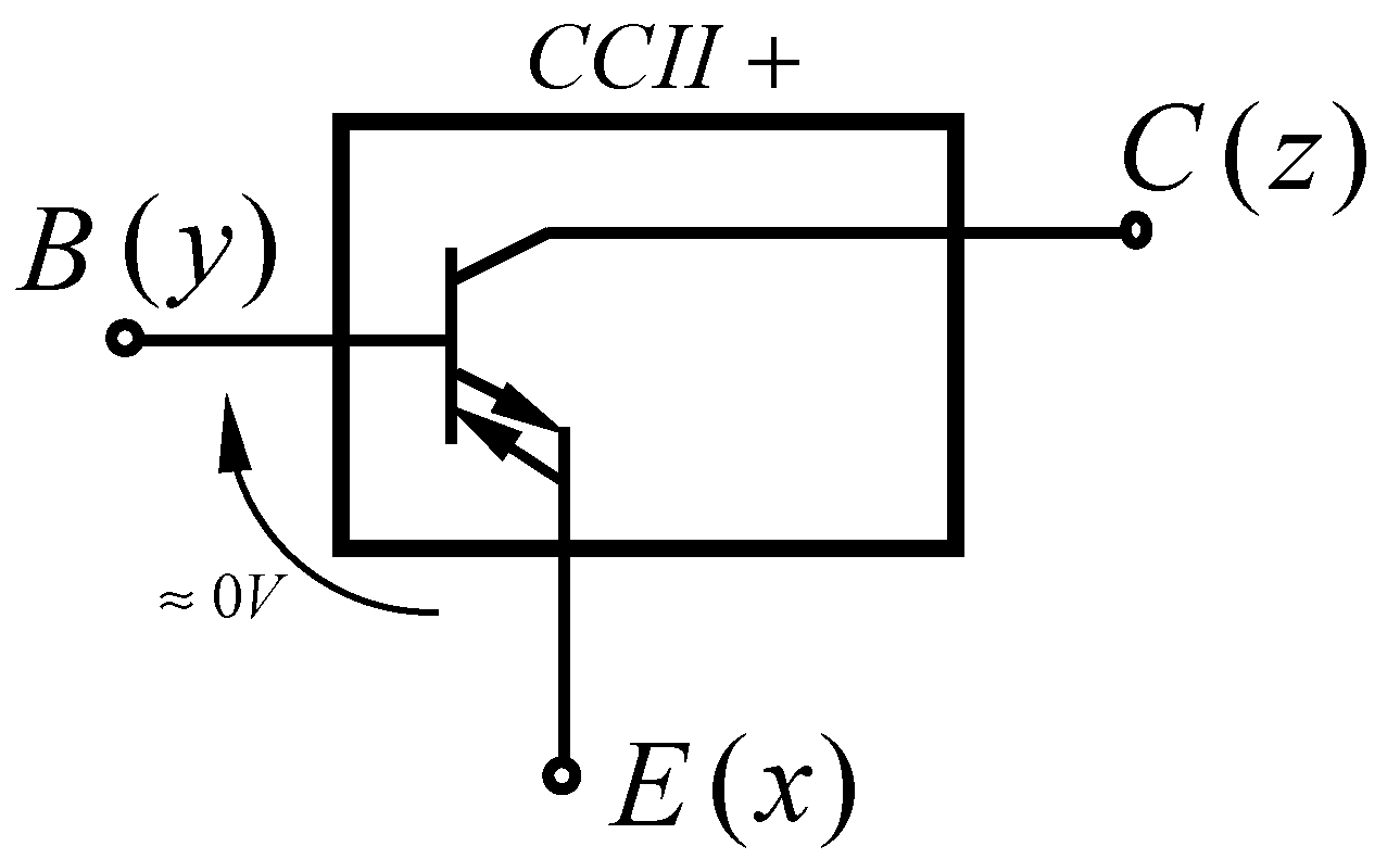
If this principle of operation is compared with the physical operation of a bipolar junction transistor (BJT), it can be concluded that the CCII+ can operate both as a npn or as a pnp transistor, depending on the polarity of the input voltage v i d . The difference is that as the v i d increases, the output current i z also increases, but its direction is opposite to the direction of the equivalent collector current of the bipolar transistor. Figure 2 shows the structure of a CCII+, represented as a bipolar transistor, but with two directions for the equivalent emitter current. In this case, the base of the transistor corresponds to the terminal y of the conveyor, the emitter of the transistor corresponds to terminal x, and the collector of the transistor corresponds to terminal z. At a quiescent operating point, i.e., vi = 0 (applied to the base or emitter according to ground), the voltage between the equivalent base and emitter is approximately equal to zero, unlike Si bipolar transistors, for which the voltage UBE has to be set from ±0.6 to ±0.7 V. The quiescent equivalent emitter and collector current is different from zero.
Other important advantages of using the CCII+s as bipolar junction transistors are the ability to obtain high input and output resistance (typically several hundred kilohms) for equivalent collector (or emitter) current of the order of a few milliamperes. Moreover, the transconductance is several tens of mA/V. These properties of the CCII+s make it possible to realize basic amplification circuits of single-stage and multistage circuits, in which bipolar transistors are replaced by monolithic current conveyors [18].
Based on the CCII+s, by adding an output buffer converting the equivalent collector current in voltage, wideband Current-Feedback Operational Amplifiers (CFOAs) with an external terminal z (or four-terminal amplifiers) are obtained. Moreover, this type of wideband amplifier is implemented as four-pole commercially available integrated circuits (ICs). Examples of integrated circuits of this type are AD844 (from Analog Devices), OPA861 (from Texas Instruments), and LT1228 (from Analog Devices, formerly Linear Technologies). In addition to the commercially available four-terminal amplifiers, there are also amplifiers of this type that contain several terminals of type y, several terminals of type x, or several terminals of types z and o (terminals after the output buffer) [8,22,23,24,25]. This makes it possible to obtain variants of active filters and oscillators with diverse functional capabilities and improved stability. For example, in [22] a special CMOS-based CFOA circuit is proposed which has one x and y type terminal each but has four z type terminals (z1, z2, z3, and z4) as well as one w terminal (or o). Based on the proposed integrated circuit, a universal active filter circuit with a cutoff frequency of up to 12.7 MHz is proposed in the same publication. In this case, all passive components (resistors and capacitors) are connected to the ground and there are no closed loops. As a result, stable operation over a wide frequency range can be more easily achieved.
Figure 3a,b show the symbol representation and the small-signal equivalent circuit of the CFOA with an external terminal z. For the circuit shown in Figure 3b, the elements r y and C y simulate the input impedance of the noninverting input, and the elements r z and C z simulate the output impedance of the CCII+ and the equivalent input impedance of the buffer.

3. Theoretical Analysis of the Proposed Electronic Circuits

3.1. Structure of the Electronic Circuits

For the development of the LC oscillators with monolithic CCII+s, it is based on the analogy with bipolar transistors discussed in the previous section, as well as the structure of well-known three-point LC oscillators [20], using transistors as active elements. Initially, three-point LC oscillators are implemented as circuits based on vacuum-tube lamps [26]. The electronic circuits using transistors are later synthesized [27], initially using bipolar transistors connected in a common-emitter circuit, which provided a 180-degree phase shift between the base and the collector at low frequencies. These circuits are established as the basic structures from which all other oscillator circuits are built. In particular, the three-point LC oscillators are transformerless analog circuits in which the bipolar or MOS transistor is connected to three points of the parallel-tuned LC circuit (a resonant LC circuit or a tank circuit (or simply LC tank)), the impedance of which is divided into three parts: Z 1 , Z 2 , and Z 3 (Figure 4). At the same time, each of these parts can be represented as a sequentially connected resistive and reactive composition, i.e., Z i = r i + j X i , where i = 1 , 2, and 3.
In order to ensure high-frequency stability, the individual elements of the electoral circuit must have a high-quality factor, i.e., r i < < X i , then Z i j X i . Under these conditions and at i C < < i o ( i o —loop current), the equivalent impedance of the resonant LC circuit is
Z o e = U ˙ C E I ˙ C X 1 X 2 + X 3 i = 1 3 r i + j X 1 + X 2 + X 3 ,
where i = 1 3 r i = r 1 + r 2 + r 3 is the total resistance of the losses in the circuit.
The self-oscillation of the circuit in Figure 4 occurs at a frequency close to the resonant frequency of the LC tank, where the denominator of Formula (1) must satisfy the equality
X 1 + X 2 + X 3 = 0   or   X 2 + X 3 = X 1 .
Then, the equivalent resistance of the LC tank is
r o e X 1 2 i = 1 3 r i .
The transmission coefficient of the positive feedback in the generalized circuit in Figure 4 is formed by the elements of the LC tank and has the form
β ˙ + = U ˙ B E U ˙ C E Z 2 Z 2 + Z 3 X 2 X 2 + X 3 .
After substituting (2) into (4) for the coefficient β ˙ + at a frequency close to the resonant frequency, Equation (5) is obtained:
β ˙ + = X 2 X 1 .
Based on Beckhausen’s criterion [19,20] for the amplitude and phase self-oscillation condition of the circuit in Figure 4, the following equations are obtained:
g m r o e β + = 1
and
π + ϕ S + ϕ Z o e + ϕ β + = 2 π ,
where g m is the transconductance of the BJT.
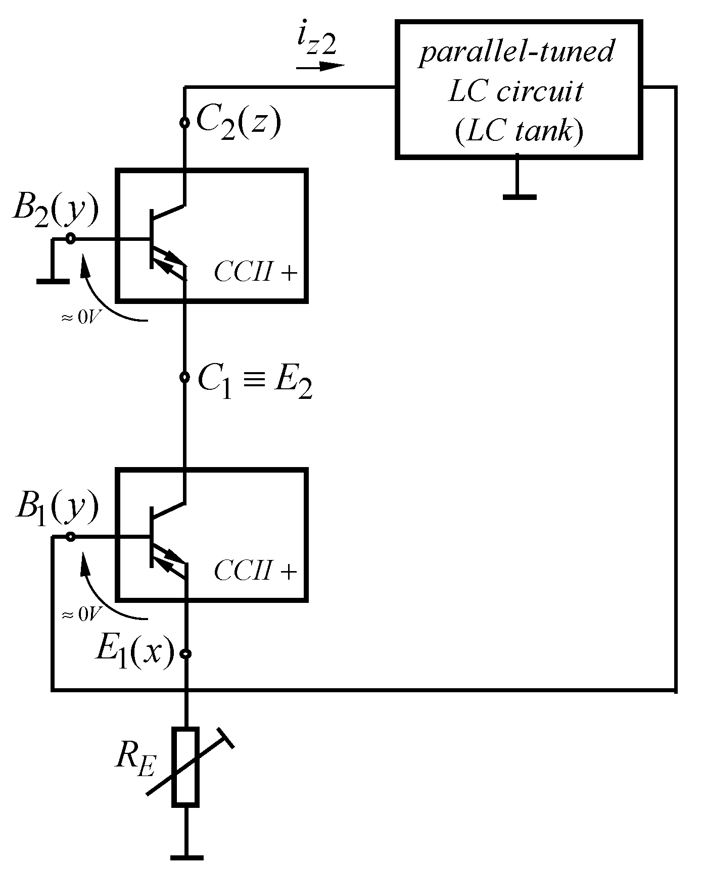
At frequencies significantly lower than the cutoff frequency of the transistor, ϕ S = ϕ Z o e = 0 and ϕ β + = π . Therefore, in order to self-oscillation the circuit, the voltage obtained from the feedback at the base of the transistor must occur with a phase shift exactly equal to 180° according to the collector voltage. It follows from Formula (5) that this condition can be fulfilled only if Z1 and Z2 are inductors or capacitors. Moreover, X3 must be of the opposite type of X1 and X2, for the fulfilment of (2). Then, if in the circuit in Figure 4, the bipolar transistor is directly replaced by a CCII+ (Figure 2) oscillations will not occur, since the voltage between the equivalent base and collector in CCII+s has the same initial electrical phase angle. As a result, in order to obtain an oscillator circuit, an additional amplifier stage is required to provide the necessary phase shift between the input and output of the amplifier function block. In this case, the first amplifier stage can be based on a common emitter equivalent circuit (CE amplifier), and the second stage based on a common base equivalent circuit (CB amplifier). In this way, the well-known circuit of cascade amplifier OE–OB is obtained, in which the two stages are connected in series by the DC mode of operation and in cascade by the AC mode of operation. The generalized structure of a two-stage oscillator circuit using CCII+s is given in Figure 5. The voltage gain is approximately determined by the ratio r z 2 / R E , where R E is a grounded resistor that can be used for tuning the value of the voltage gain. On the other hand, the transmission ratio of the output current to the input voltage of the amplifier block in the oscillator is determined by the Formula
A Y = i Z 2 u y 1 1 R E + r x + R E r x r z + r x 2 r z .
As can be seen, the transmission coefficient A Y can be changed by tuning the value of the resistor RE without changing the parameters of the LC tank.
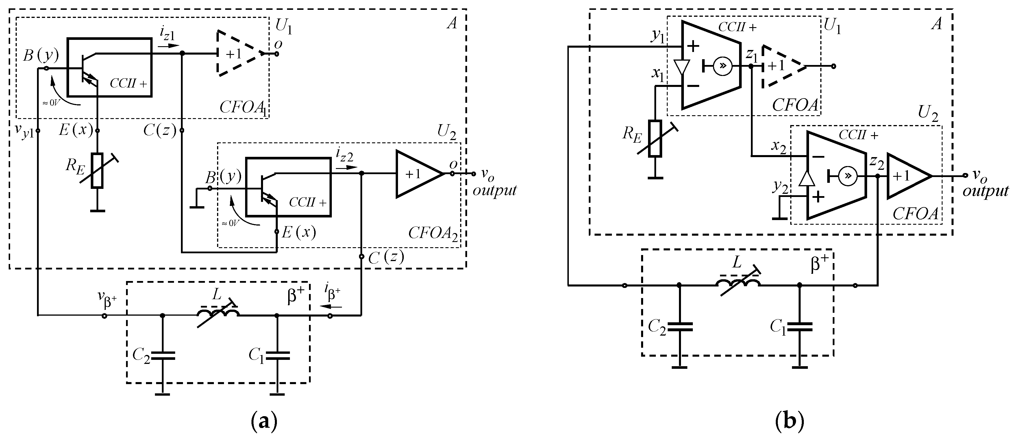
The obtained LC oscillators are shown in Figure 6a, Figure 6b, and Figure 7, respectively. The LC oscillator in Figure 6b is implemented using two current conveyors, presented as equivalent BJT. For this representation, the high-impedance output C of the first equivalent transistor U1 is connected to the low-impedance input E of the second equivalent transistor U2. As a result, the two inputs of the first equivalent transistor exchange roles, i.e., terminal B (or y) become inverting and terminal E (or x) becomes noninverting, as in standard bipolar transistors. To terminal E, of the first equivalent transistor, a variable resistance RE to adjust the amplitude of the output sinusoidal signal is connected. Unlike the LC oscillators with classical operational amplifiers, which require the inclusion of a special circuit for an amplitude-control circuit in the proposed oscillators, there is a nonlinear dependence of the iz versus vid for amplitude control. The proposed LC oscillators can be seen as self-limiting oscillators. A terminal B of the second equivalent transistor is connected to the ground.
The LC tank is connected between terminal C of the second equivalent transistor and terminal B of the first equivalent transistor. As a result, the positive feedback loop is closed. The output sinusoidal signal is obtained after the buffer of the second equivalent transistor. This method of electrical connection allows avoiding the influence of the load parameters on the parameters of the frequency-selective feedback network. Figure 6b shows a circuit diagram, the active elements, represented by CFOAs with external terminal z. The circuits in Figure 6a,b can be considered as circuit variants of the Colpitts oscillator. Compared to the Colpitts circuit configuration with discrete transistors, the proposed oscillators use a smaller number of passive elements and there are no additional resistor dividers and coupling capacitors to determine the operating point of the active elements. Also, for the proposed circuits, the output signal is produced at the output of a buffer (voltage follower), as a result of which the influence of the load parameters on the elements of the tank circuit is minimized.
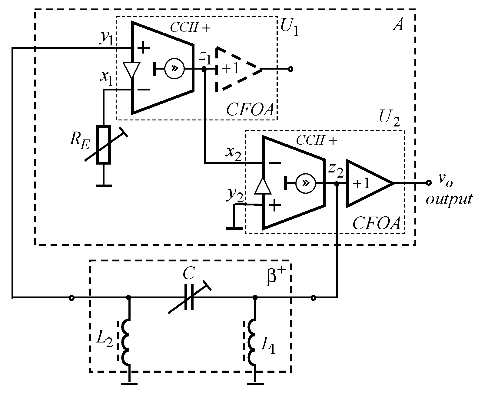
In a similar technique, the circuit in Figure 7 is synthesized. It includes frequency-selective inductive feedback, consisting of two inductors and one capacitor. This circuit can be considered a variant of the Hartley oscillator with discrete transistors.
One of the possible practical applications of the proposed oscillators, according to the grant number KP-06-DO02/2 under the ERA.NET RUS+ program, is the synthesis of electronic circuits of gas sensors using surface acoustic wave (SAW) resonators, as gas-sensitive elements. The SAW resonators are equivalent to the crystal resonators and include a piezoelectric substrate (such as LiNbO3, which provides a broader temperature range of relatively stable piezoelectric coefficients) and two groups of specific metal interdigitated electrodes (IDTs) [20,28,29]. The geometry and dimensions of the IDTs, such as fingers distance, length, and aperture, determine the frequency of the SAW resonators. The general structure of the SAW resonator for low frequencies (up to 1 MHz) is given in Figure 8. To create a gas sensor based on the SAW resonator, the sensing layer is deposited on the IDT transducers or between them. The sensing layer propagates the surface acoustic waves with different velocities according to its mass loading with the analyte whose concentration has to be measured.
Based on the operational principle of the SAW resonator in Figure 9 the equivalent circuit diagram as a “Pseudo two-port” electrical connection is given. In Figure 9, the passive components r, L, and C define the parameters of the series resonance, and the parasitic capacitance C0 reflects the capacitance between the two groups of metal fingers with the piezoelectric plate as a dielectric. To use this circuit as a resonant circuit in a LCO1, impedance transformations are performed, whereby the series resonance circuit is converted into a parallel circuit composed of an equivalent inductance and an equivalent resonant resistance:
L e = L e r 2 + ( ω L e ) 2 ( ω L e ) 2 ω L e > > r L e   and
r r e = r 2 + ( ω L e ) 2 r ω L e > > r ( ω L e ) 2 r ,
where L e = L 1 ω s 2 ω Q 2 (the angular frequency ω Q is specified by the certain manufacturer, at the specified external load capacitance, as it is slightly higher than the frequency of the series resonance ω s , and then L e < L ).
Based on the electronic circuits, represented in [28,29,30,31], after substituting the equivalent circuit of Figure 9 into the circuit of Figure 6b, the oscillator circuit (LCO3) in Figure 10 is obtained. In this circuit, the SAW resonator behaves as an equivalent inductance of value L e . Also, to compensate for the effect of the parasitic capacitance C0, a coil LT with variable inductance is added in parallel with the resonator, the value of which is adjusted according to the value of C0. In this case, the oscillation frequency can be found by the following analytical expression
ω 0 = 1 L e C 1 C 2 C 1 + C 2 ,
where C 1 = C 1 + C z + C M ( C M is the board parasitic board capacitance with a typical value equal to 3…5 pF for the used board substrate) and C 2 = C 2 + C y + C M .
Therefore, changing the concentration of the analyte on the surface of the SAW resonator should lead to a change in the frequency ω Q and, hence, to a change in the value of the equivalent inductance L e . This change should lead to a change in the oscillation frequency, according to Formula (9).

3.2. Circuit Analysis

For a certain frequency f 0 = ω 0 / 2 π , the loop gain L in the circuit with positive feedback is
L ( j ω 0 ) A ( j ω 0 ) β + ( j ω 0 ) = 1   or A ( j ω 0 ) = 1 / β + ( j ω 0 )
in which sinusoidal oscillations may occur at the output. In expression (10) the coefficient A = iz2/vy1 is the open-loop gain of the amplifier and β+ = vβ+/iβ+ is the transmission coefficient of the positive feedback (or feedback factor).
The proposed circuit configurations’ basic parameters (amplitude and oscillation frequency) can be obtained from the analysis of the corresponding characteristic equation of the loop gain. Obtaining the characteristic equation can be done in two ways. Firstly, the CCII+ is replaced by a linear electrical model (Figure 3) and as a result, a linear equation is obtained for the steady-state mode of operation. For the second way, the nonlinear transmission characteristic of the selected sample CCII+ should be compiled and the resulting mathematical expression substituted in the equation for the loop gain. In this way, formulas for the amplitude and frequency of the output signal can be found with exact values [32,33]. The first approach using linear models was chosen for the research carried out in this work. This approach is more often used in the development of oscillators, since regardless of the specific parameters of each instance of an active element analytical expressions for the basic parameters can be determined; if the independence of the tuning is ensured, it is possible to relatively accurately obtained the desired value of the frequency and especially the amplitude of the output signal. Furthermore, it is unnecessary to characterize every instance of an active element of a given type.
Using the small-signal equivalent circuit of a CFOA (Figure 3b) by the nodal method for the linear characteristic equation in a steady-state operation of the LCO1 is found:
s 3 C 1 C 2 L + s 2 ( C 2 L / r o e ) + s ( C 1 + C 2 ) +   or + 1 r o e + 1 R E + r x + R E r x / r z = 0 ,
where r o e = r z | | r r e | | r y is the equivalent resonance resistance, r r e ρ 2 / r L , ρ = L / ( C 1 | | C 2 ) is the characteristic resistance of the LC tank circuit (or the equivalent quality factor is Q e ρ / r L ), and r L is the ohmic resistance of the selected inductor L.
Substituting s = jω gives
1 r o e + 1 R E + r x + R E r x / r z ω 2 C 2 L r o e +   or + j ω ( C 1 + C 2 ) ω 3 C 1 C 2 L = 0 .
In order for oscillations to occur at the output of the circuit, both the real and the imaginary parts of the above expression must be equal to zero. Equating the imaginary part to zero gives the following formula for the frequency of oscillations:
ω 0 = 1 / L C 1 C 2 / ( C 1 + C 2 ) .
Equating the real part to zero gives the following formula for the oscillation condition:
r o e R E + r x + R E r x / r z = C 2 C 1 .
According to a similar approach for the LCO2 (Figure 7) theoretical analysis is performed, in which the linear characteristic equation in a steady-state operation is
s 3 1 r o e + 1 R E + r x + R E r x / r z + s 2 L 1 + L 2 L 1 L 2 + s 1 r o e L 2 C + 1 L 1 L 2 C = 0 .
Substituting s = jω gives
1 L 1 L 2 C ω 2 L 1 + L 2 L 1 L 2 + j ω r o e L 2 C ω 3 1 r o e + 1 R E + r x + R E r x / r z = 0 .
Based on Formula (15), the frequency of oscillations and the ratio for determining the amplitude of the output signal is obtained:
ω 0 = 1 / C ( L 1 + L 2 )   and
r o e R E + r x + R E r x / r z = L 1 L 2 .
For the occurrence of oscillations in the proposed electronic circuits, it is necessary that the loop gain is greater than unity, and the gain A must be greater than C2/C1 or L1/L2. Moreover, the first stage of the amplifier part does not amplify the input voltage, and the amplification is obtained through the second stage according to the value of the resistance RE, which has the function of equivalent emitter stabilization. In both cases, oscillators are started by tuning the RE. The self-limiting process is obtained by the nonlinear internal mechanism of the used equivalent BJTs. The input differential voltage that exists between input terminals x and y is given by [34] v x y = ϕ T ln ( i int ( t ) / I b i a s ) , where ϕ T = k T / q is the thermal voltage, i int ( t ) is the internal current through the bipolar transistors (connected to a terminal x) of the input stage and I b i a s is the DC bias current of the CCII+. If the input current i(t) is zero, the internal currents through the transistors with emitters, connected to a terminal x, will be equal to each other. The value of the driving current i(t) is v(t)/RE, and this current determined the change in the value of i int ( t ) [35]. As a result, at small current values of the i int ( t ) , the voltage drop vxy increases almost linearly, while at larger values of the i int ( t ) it increases less, i.e., the increase in the voltage is limited, at which the amplitude of the output signal is also obtained with limited value.
Based on the analysis of the phase-frequency response of the loop gain L in the LCO1 and LCO2, the coefficient of the frequency stability in a wide frequency range is obtained
S F = d Φ ( u ) d u u = 1 2 Q e ,
where u = ω / ω 0 is the normalized value of the frequency and Φ ( u ) = arg [ L ( u ) ] is the phase-frequency response of the loop gain for the normalized frequency value.
As can be seen from Formula (17), the coefficient of frequency stability is approximately equal to twice the value of the equivalent quality factor. As a result, in comparison to three-point LC oscillators with single discrete or integrated transistors, greater stability in the frequency of the output signal in a relatively wide frequency range (up to several tens of megahertz) can be obtained for the proposed circuit configurations.

4. Simulation and Experimental Results

To verify the efficiency of the proposed circuits, detailed experimental studies were performed. For the implementation of the LC oscillators as active elements were used CFOAs AD844A (supplied with ±15 V) [36], which have an external terminal z between the first and second stage of the internal electrical circuit. Thus, a bandwidth of about 100 kHz to 10 MHz can be provided. Higher oscillation frequencies can be obtained, for example, by using OPA861 or LT1228. The AD844A (with unity-gain bandwidth B1 ≈ 60 MHz at Gain = −1) was chosen as the active element because for OPA860 at frequencies higher than 80 MHz or gain less than +5 it becomes unstable and can start undetermined oscillations. For an IC LT1228 (with B1 ≈ 100 MHz) the internal structure uses specific circuitry techniques and the designed analog circuits require a relatively large number of external passive components. In the construction of the oscillators through-hole passive components were used, whose values are selected depending on the chosen electrical parameters. The trimming potentiometer RE = 5 kΩ or adjustable inductors (or capacitors) were used to set the amplitude and frequency of oscillation, respectively.
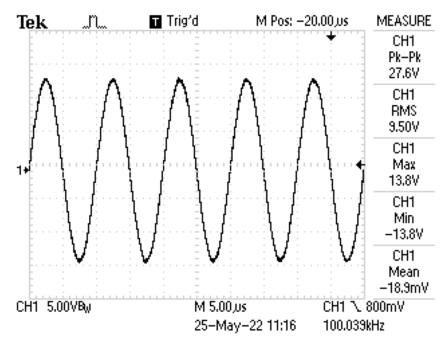
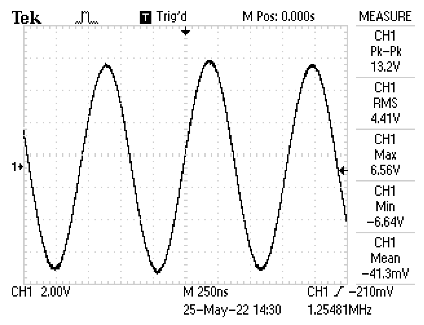
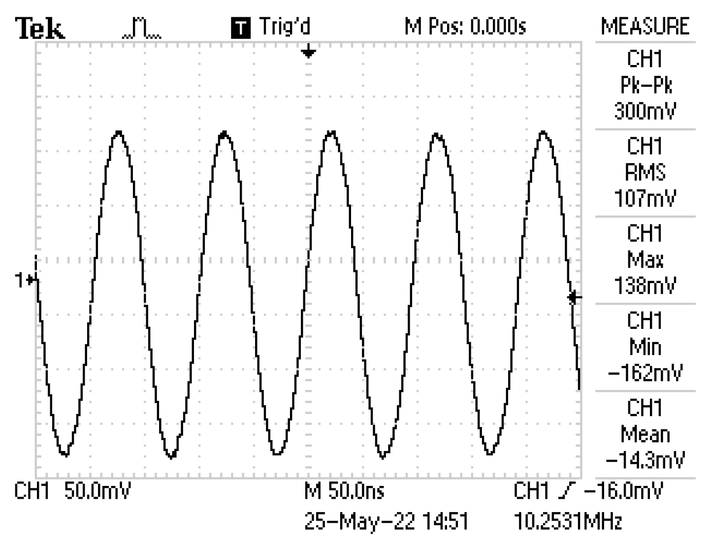
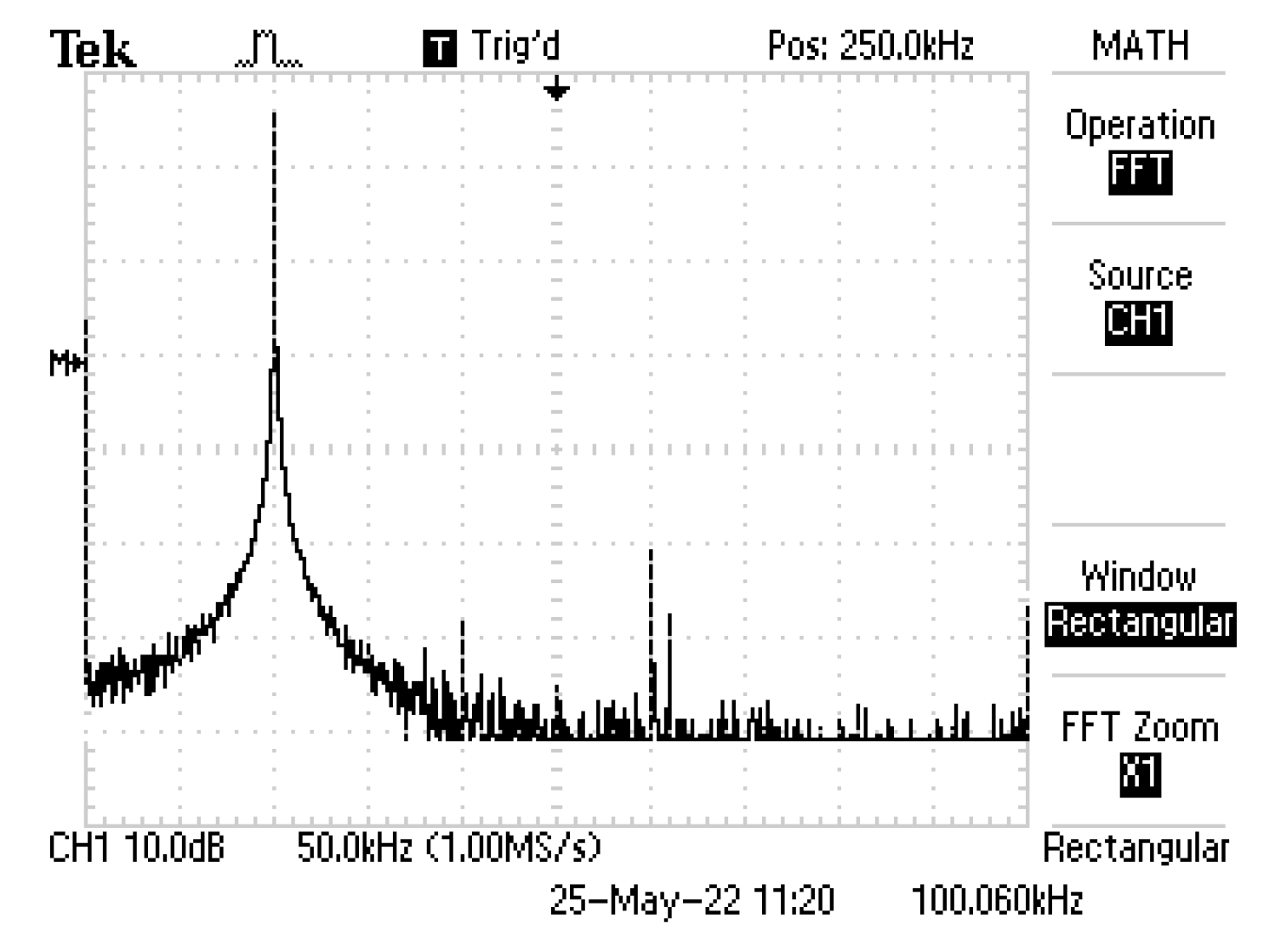
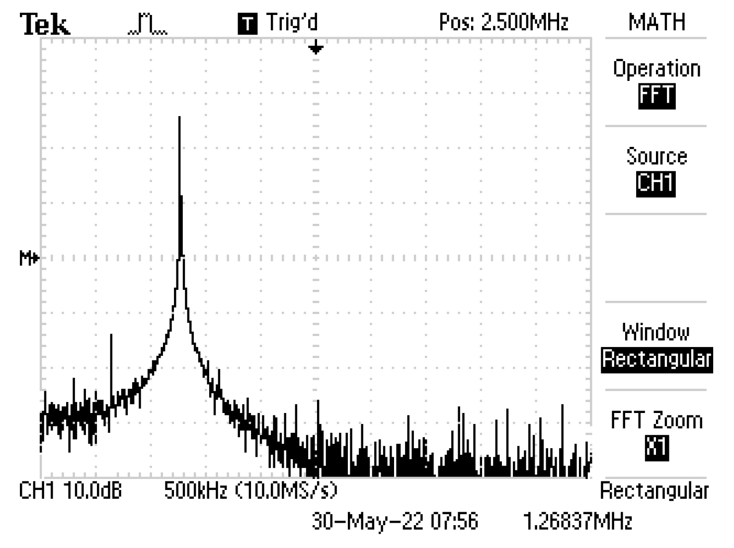
In Figure 11, Figure 12 and Figure 13 for the LCO1 the output sinusoidal signals are given for oscillation frequencies 100 kHz, 1.25 MHz, and 10 MHz. Figure 14 shows the spectral characteristic of the signal at a frequency equal to 100 kHz. For the three frequency values f 0 = ω 0 / 2 π , the feedback factor is chosen to be equal to 10, thus providing a sufficient distance from the unity-gain bandwidth and the influence of parasitic high-frequency poles. Thus, the possible value for the oscillation frequency at the chosen op-amp is limited to about 10 MHz. Under this condition, for the highest of the three frequencies, the capacitance of the capacitors is chosen to be at least 50 times the parasitic board capacitance, which is typically not less than 2 pF when using FR4 PCB material. As a result, the frequency of oscillations for the proposed circuits can be determined with sufficient accuracy by the external passive elements and not depending on the inertial properties of the selected CFOA and their changes when the parameters are altered by various destabilizing factors.
The obtained experimental results confirm the theoretical analyses performed, as the coefficient of nonlinear distortions is below 5%. Figure 15 and Figure 16 show experimental results for the output signal and the corresponding spectrum for the LCO2 at an oscillation frequency of 1.25 MHz. For the second circuit, a stable output signal is also obtained with small nonlinear distortions. The output signals presented in the figures above are for the maximum possible output voltage swing.
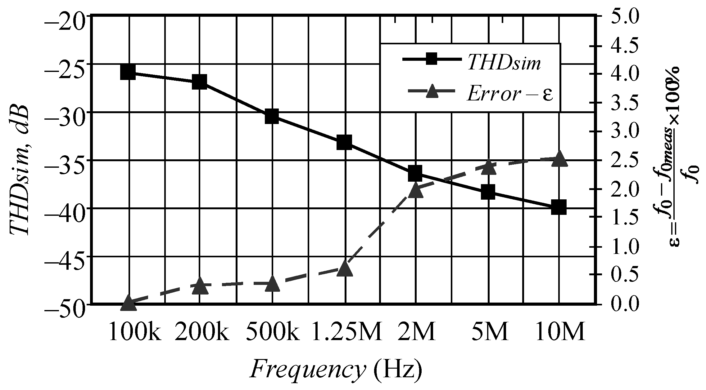
Figure 17 shows the simulated value of the nonlinear distortions versus the oscillation frequency and the relative error of the deviation from the chosen frequency value of the LCO1. The simulations were performed by the program OrCAD PSpice® 9.0 Cadence Design Systems, Inc., San Jose, CA 95134, USA) and using models from standard libraries. The relative error increases with the increasing frequency f0meas (from 100 kHz to 10 MHz), while the nonlinear distortions (or THD–Total Harmonic Distortion) decrease (from 5% to 1%), as the maximum value of the amplitude of the generated signal decreases due to the influence of parasitic board effects and noise level.
Also, when the ambient temperature changes from 25 °C to 65 °C, the total frequency shift is approximately equal to 0.4% or 0.01%/°C. Further reduction in the oscillation frequency variation by temperature can be achieved by using precision surface mount passive components (such as NP0 capacitors) in the resonant LC circuit.
The stability of the oscillation frequency is determined by the frequency instability for given values of the passive components in the resonant LC circuit of the proposed circuits. The instability is also defined as a phase noise in the oscillator circuits. Analytically, the phase noise is related to the frequency stability coefficient, given by Formula (17). Moreover, this value is directly proportional to the equivalent quality factor of the circuit. The frequency instability of the LCO1 was determined experimentally by measuring the frequency variation for room temperature with a digital frequency counter and via a standard interface cable, such as RS232 or USB; the signal was applied to standard ports of a personal computer. The measured values in tabular form were processed in the MS Excel program so that for each value of the set frequency of oscillations f 0 , n o m the maximum deviation Δ f max was determined. For each frequency value, the frequency instability is determined according to the formula δ d B = 20 log 10 ( Δ f max / f 0 , n o m ) . Additionally, for visualization of the shape of the output signal a digital storage oscilloscope—TDS1012B and an Instek GFC-8010H frequency counter are used to control the value of the frequency. To provide the power supply voltages for the monolithic CFOA AD844A, a DC linear power supply HY3005D-3 was used, providing DC voltages of ±15 V.
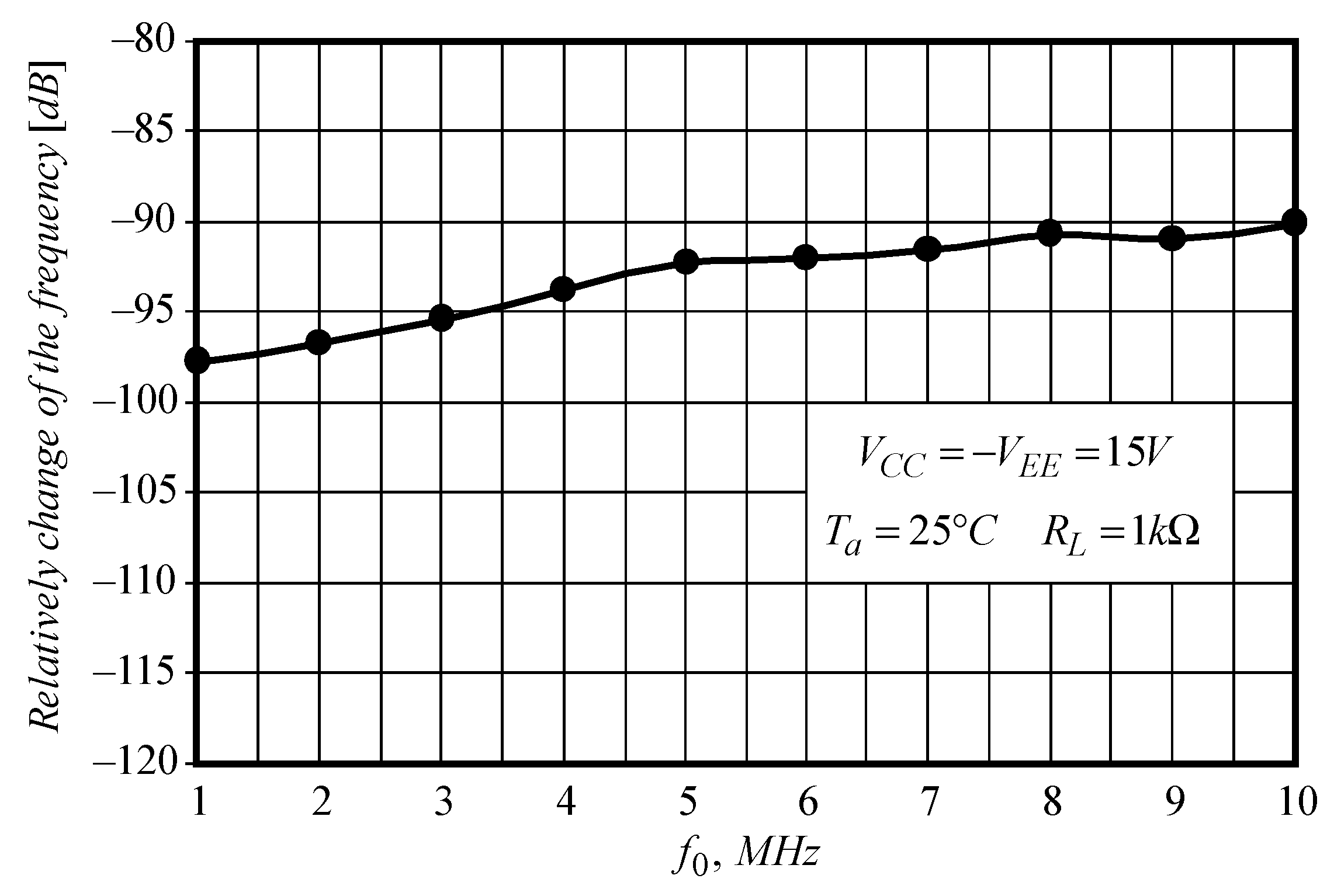
For LCO1, Figure 18 gives the relative value of frequency instability in decibels [dB] for the frequency range from 1 MHz to 10 MHz. As can be seen, the value of the frequency instability is changed from −90 dB to −97 dB within the frequency range, which is acceptable considering the manufacturing tolerances of the parameters of the passive components. For the frequency range from 100 kHz to 1 MHz, the value of frequency instability is obtained with a value approximately within range −(100…105) dB, due to the smaller influence of parasitic effects without a relatively large change in the equivalent quality factor of the circuit. The frequency instability for two frequencies 1 MHz and 10 MHz was also investigated in a laboratory thermostatic chamber, and the ambient temperature was changed from 25 °C to 65 °C. In the way presented above, the relative change in frequency was determined, and an increase in frequency instability was found with increasing temperature to about −85 dB. The increased instability is mainly a result of the temperature drift of the electrical parameters of the passive elements. Also, careful design of the circuit board with the sample circuit studied in the placement of components and wiring of electrical connections also has some effect on the frequency instability, especially over wider temperature variation ranges.
A comparison of the proposed circuit configurations (LCO1 and LCO2) with some typical structures of oscillator circuits using different types of operational amplifiers is given in Table 1. In doing so, the comparative analysis begins initially with the classical circuits of three-point LC oscillators (Colpitts and Hartley oscillators), presented with an analysis of various aspects of their behavior in [18,19,20]. Without any doubt, these circuits can provide oscillation frequencies up to several GHz. At the same time, the amplitude of the output signal, depending on the power supply voltage, can vary from several hundred millivolts to several volts. As a disadvantage of the classic three-point circuits, it can be stated that additional passive components (resistors and capacitors) connected to the transistor and the resonant LC circuit are needed to establish the operating point of the transistor, as well as to provide the frequency tunability or the amplitude tunability. As a result, the equivalent quality factor is lowered, and from there the phase noise level is increased. The typical values for the Q-factor at frequencies up to about 100 MHz can be obtained with values up to about 50. Also, when connecting an external load, various techniques are used, often requiring the addition of new functional blocks and amplifying stages, to ensure the independence of the parameters of the resonant LC circuit. To a large extent, these drawbacks are avoided in the proposed circuits, since monolithic amplifiers are used, which limits the number of discrete elements used. In addition, the stability factor is doubled compared to the value for three-point oscillators. Regarding the maximum value of the oscillation frequency, it can be relatively easily increased when using some high-frequency amplifiers, and the oscillation frequency can be reached up to 100 MHz.
Regarding circuits using operational amplifiers, the proposed circuit configurations provide a higher frequency of oscillation, a relatively smaller number of active and passive components [14], and a significantly higher value for the stability factor or smaller phase noise [10,14,24]. Also, for some of the known circuits [10,11,13], there are known dependencies when setting some of the basic electrical parameters, such as the amplitude of the output signal and the frequency of oscillations. For the oscillator circuits using specialized integrated circuits of CCII+s with several input terminals (x or y type) and several output terminals (z or w type) [8,22,23,24], a relatively small number of passive components are used, and there are possibilities for independent adjustment of the amplitude and frequency of oscillations. Despite the stated advantages of these circuits, the oscillation frequency is also limited to a few MHz and their purpose is for relatively specialized applications.

5. Conclusions

In this paper, two electronic circuits of three-point self-limiting LC oscillators using monolithic CFOAs with an additional compensation pin (Z) have been proposed. Both circuits show a good match between the measured and simulation results for the basic parameters, the differences being mainly due to the component manufacturing tolerances. In comparison with the classical Colpitts and Hartley circuits, based on various types of transistors, the structures of the proposed oscillators have the following characteristics: (1) Lack of additional resistor dividers with coupling capacitors or additional systems of current mirrors to set the operating point of the transistors; (2) Minimal influence of the load over the parameters of the frequency-selective network; (3) Independent amplitude and frequency tuning of the output signal ensured.
Future work will be related to the design of circuit configurations based on the proposed LC oscillators, working together with thin film gas sensors based on surface acoustic waves.

Funding

This research was funded by the Bulgarian National Science Fund, grant number KP-06-DO02/2 form 2020, under the ERA.NET RUS + project.

Data Availability Statement

The data presented in this study are available on request from author.

Acknowledgments

The author wishes to thank the reviewers for their helpful suggestions and comments concerning this work.

Conflicts of Interest

The author declares no conflict of interest.

References

  1. Radfar, M.; Green, M.M. An LC voltage-Controlled Oscillator with Supply Sensitivity Compensation Method. In Proceedings of the IEEE 60th International Midwest Symposium on Circuits and Systems (MWSCAS), Boston, MA, USA, 6–9 August 2017. [Google Scholar]
  2. Chaharboor, M.; Ghonoodi, H. Improved resonator phase shift in passive and active coupled LC Quadrature Oscillator. In Proceedings of the Iranian Conference on Electrical Engineering (ICEE), Tehran, Iran, 2–4 May 2017. [Google Scholar]
  3. Rathore, T.S. Synthesis and classification of LC oscillators. In Proceedings of the 2nd International Conference on Communication Systems, Computing and IT Applications (CSCITA), Mumbai, India, 7–8 April 2017. [Google Scholar]
  4. Proano, E.; Navarro, M.; Sanchez, A.; Benitez, D.S. On the Design of Active LC Oscillators Using Small-Signal Model Network Analysis. In Proceedings of the IEEE Colombian Conference on Communications and Computing (COLCOM), Medellin, Colombia, 16–18 May 2018. [Google Scholar]
  5. Kira, A.; Elsayed, M.Y.; Allidina, K.; Chodavarapu, V.P.; El-Gamal, M.N. A 6.89-MHz 143-nW MEMS Oscillator Based on a 118-dB? Tunable Gain and Duty-Cycle CMOS TIA. Electronics 2021, 10, 21. [Google Scholar] [CrossRef]
  6. Salem, S.B.; Saied, A.B.; Masmoudi, D.S. High-performance Current-Controlled Quadrature Oscillator Using an optimized CCII. J. Microelectron. Electron. Compon. Mater. 2016, 46, 91–99. [Google Scholar]
  7. Mishra, S.K.; Upadhyay, D.K.; Gupta, M. Compact design of fractional order LC oscillator. In Proceedings of the URSI Asia-Pacific Radio Science Conference (AP-RASC), New Delhi, India, 9–15 March 2019. [Google Scholar]
  8. Agrawal, D.; Maheshwari, S. An active-C Current-Mode Universal First Order Filter and Oscillator. J. Circuits Syst. Comput. 2019, 28, 13. [Google Scholar] [CrossRef]
  9. Jaikla, W.; Adhan, S.; Suwanjan, P.; Kumngern, M. Current/Voltage Controlled Quadrature Sinusoidal Oscillators for Phase Sensitive Detection Using Commercially Available IC. Sensors 2020, 20, 5. [Google Scholar] [CrossRef]
  10. Garinto, D.; Syahriar, A.; Budiyanto, S. A Novel Op-Amp Based LC Oscillator for Wireless Communications. In Proceedings of the 46th Annual Conference of the IEEE Industrial Electronics Society, Singapore, 18–21 October 2020. [Google Scholar]
  11. Mohsen, M.; Said, L.A.; Elwakil, A.S.; Madian, A.H.; Radwan, A.G. Extracting Optimized Bio-Impedance Model Parameters Using Different Topologies of Oscillators. IEEE Sens. J. 2020, 20, 9947–9954. [Google Scholar] [CrossRef]
  12. Maheshwari, S. Realization Approach for Sinusoidal Signal Generation and Circuit with Easy Control. J. Circuits Syst. Comput. 2020, 29, 2. [Google Scholar] [CrossRef]
  13. Stornelli, V.; Barile, G.; Pantoli, L.; Scarsella, M.; Ferri, G.; Centurelli, F.; Tommasino, P.; Trifiletti, A. A New VCII Application: Sinusoidal Oscillators. J. Low Power Electron. Appl. 2021, 11, 3. [Google Scholar] [CrossRef]
  14. Borah, S.S.; Singh, A.; Ghosh, M.; Ranjan, A. Electronically tunable higher-order quadrature oscillator employing CDBA. Microelectron. J. 2021, 108, 104985. [Google Scholar] [CrossRef]
  15. Altuntas, E.; Toker, A. Realization of voltage and current mode KHN biquads using CCCIIs. Int. J. Electron. Commun. 2002, 56, 45–49. [Google Scholar] [CrossRef]
  16. Sedra, A.; Smith, K. A second-generation current conveyor and its applications. IEEE Trans. Circuit Theory 1970, 17, 132–134. [Google Scholar] [CrossRef]
  17. Barthélemy, H.; Gies, V.; Meillère, S.; Vauché, R.; Kussener, E.; Fourniol, M. CMOS voltage and current feedback opamps: A comparison between two similar topologies. Int. J. Electron. Lett. 2021, 9, 187–202. [Google Scholar] [CrossRef]
  18. Tietze, V.; Schenk, C. Operational Amplifiers. Signal Generators. In Electronic Circuits, 2nd ed.; Springer-Verlag: New York, NY, USA, 2008; Chapter 5 and Chapter 14; pp. 483–586, 843–867. [Google Scholar]
  19. Sedra, A.; Smith, K.; Carusone, T.; Gaudet, V. Oscillators. In Microelectronic Circuits, 8th ed.; Oxford University Press: Oxford, UK, 2020; Chapter 15; pp. 1066–1107. [Google Scholar]
  20. Seifart, M. Signalgeneratoren. In Analoge Schaltungen, 6 Auflage; Verlag Technik: Berlin, Germany, 2003; Chapter 18; pp. 460–484. [Google Scholar]
  21. Pandiev, I. Development of Self-Limiting LC Oscillators Using Cascade Structure of Monolithic CCIIs. In Proceedings of the 2023 30th International Conference on Mixed Design of Integrated Circuits and System (MIXDES), Kraków, Poland, 29–30 June 2023; pp. 148–153. [Google Scholar] [CrossRef]
  22. Yuce, E. Fully integrable mixed-mode universal biquad with specific application of the CFOA. Int. J. Electron. Commun. 2010, 64, 304–309. [Google Scholar] [CrossRef]
  23. Yuce, E.; Minaei, S. A first-order fully cascadable current-mode universal filter composed of dual output CCIIs and a grounded capacitor. J. Circuits Syst. Comput. 2016, 25, 1–15. [Google Scholar] [CrossRef]
  24. Kumar, A.; Paul, S. Current mode first order universal filter and multiphase sinusoidal oscillator. Int. J. Electron. Commun. 2017, 81, 37–49. [Google Scholar] [CrossRef]
  25. Safari, L.; Yuce, E.; Minaei, S. A new ICCII based resistor-less current-mode first-order universal filter with electronic tuning capability. Microelectron. J. 2017, 67, 101–110. [Google Scholar] [CrossRef]
  26. Kamphoefner, F.J. Feedback in Very-High-Frequency and Ultra-High-Frequency Oscillators. Proc. IRE 1950, 38, 630–632. [Google Scholar] [CrossRef]
  27. Oakes, J.B. Analysis of Junction Transistor Audio Oscillator Circuits. Proc. IRE 1954, 42, 1235–1238. [Google Scholar] [CrossRef]
  28. Bell, D.L.T.; Li, R.C.M. Surface-Acoustic-Wave Resonators. Proc. IEEE 1976, 64, 711–721. [Google Scholar] [CrossRef]
  29. Parker, T.E.; Montress, G.K. Precision surface-acoustic-wave (SAW) oscillators. IEEE Trans. Ultrason. Ferroelectr. Freq. Control. 1988, 35, 342–364. [Google Scholar] [CrossRef]
  30. Pasternak, M. Overtone Oscillator for SAW Gas Detectors. IEEE Sens. J. 2006, 6, 1497–1501. [Google Scholar] [CrossRef]
  31. Montress, G.K.; Parker, T.E.; Andres, D. Review of SAW oscillator performance. In Proceedings of the IEEE Ultrasonics Symposium, Cannes, France, 31 October 1994–3 November 1994; Volume 1, pp. 43–54. [Google Scholar] [CrossRef]
  32. Savov, V.; Georgiev, Z.; Todorov, T. Analysis and synthesis of perturbed Duffing oscillators. Int. J. Circuits Theory Appl. 2006, 34, 281–306. [Google Scholar] [CrossRef]
  33. Vidal, E.; Poveda, A.; Ismail, M. Describing functions and oscillators. IEEE Circuits Devices Mag. 2001, 17, 7–11. [Google Scholar] [CrossRef]
  34. Fabre, A.; Saaid, O.; Wiest, F.; Boucheron, C. Current controlled bandpass filter based on translinear conveyors. Electron. Lett. 1995, 31, 1727–1728. [Google Scholar] [CrossRef]
  35. Fabre, A. Dual translinear voltage/current convertor. Electron. Lett. 1983, 19, 1030–1031. [Google Scholar] [CrossRef]
  36. 60 MHz 2000 V/μs Monolithic op amp AD844—Datasheet. Analog Devices, Norwood, MA, USA, 2017. Available online: https://www.analog.com/en/products/ad844.html (accessed on 13 July 2023).
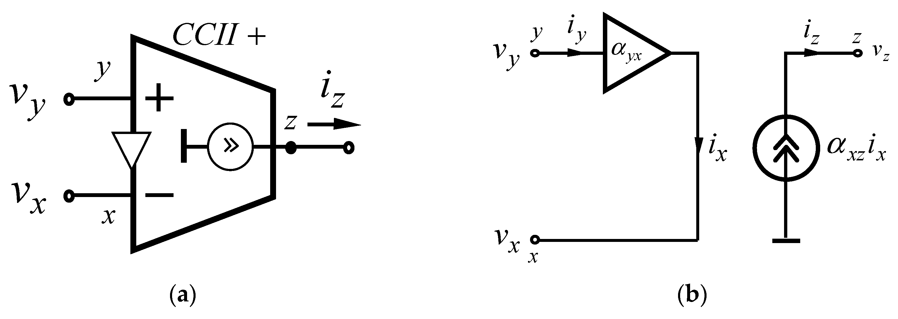
Figure 1. Positive second-generation current conveyor (CCII+): (a) Symbol representation; (b) Ideal equivalent circuit.
Energies 16 06226 g001
Figure 2. Structure of a CCII+ represented as a BJT.
Energies 16 06226 g002
Figure 3. Current-Feedback Operational Amplifier (CFOA), with external terminal z (or with compensation pin (Z)): (a) Symbol representation as a cascade structure; (b) Small-signal equivalent electrical circuit.
Energies 16 06226 g003
Figure 4. Circuit diagram of three-point LC oscillator, using NPN bipolar transistor as an active component (Adapted from [20,26,27]).
Energies 16 06226 g004
Figure 5. Generalized structure of a two-stage oscillator circuit using two CCII+s, represented as a cascade (common emitter-common base) configuration.
Energies 16 06226 g005
Figure 6. LC oscillator with frequency-selective capacitive feedback network (LCO1): (a) Circuit diagram using monolithic CCIIs, represented as BJTs; (b) Circuit diagram using CCIIs, represented as a part of CFOA, with a compensation pin (Z) or with an output terminal z.
Energies 16 06226 g006
Figure 7. LC oscillator with inductive positive feedback network (LCO2), using CFOAs with a compensation pin (Z).
Energies 16 06226 g007
Figure 8. Structure for a low-frequency SAW resonator—top view.
Energies 16 06226 g008
Figure 9. Equivalent electrical circuits of “pseudo two-port” SAW resonator—impedance transformation.
Energies 16 06226 g009
Figure 10. CFOA-based LC oscillator with SAW resonator and two grounded capacitors (LCO3).
Energies 16 06226 g010
Figure 11. The output waveform of the LCO1 at 100 kHz with C1 = 2.53 nF, C2 = 25.3 nF, and L = 1 mH.
Energies 16 06226 g011
Figure 12. The output waveform of the LCO1 at 1.25 MHz with C1 = 120 pF, C2 = 1.2 nF, and L = 150 μF.
Energies 16 06226 g012
Figure 13. The output waveform of the LCO1 at 10 MHz with C1 = 103 pF, C2 = 1.03 nF and L = 2.7 μH.
Energies 16 06226 g013
Figure 14. The output spectrum of the LCO1 at a frequency equal to 100 kHz.
Energies 16 06226 g014
Figure 15. The output waveform of the LCO2 at 1.25 MHz with L1 = 15 μH, L2 = 1.5 μH, and C = 1 nF.
Energies 16 06226 g015
Figure 16. The output spectrum of the LCO2 at 1.25 MHz.
Energies 16 06226 g016
Figure 17. THD and error versus oscillation frequency.
Energies 16 06226 g017
Figure 18. Frequency instability of the LCO1 within a frequency range from 1 MHz to 10 MHz.
Energies 16 06226 g018
Table 1. Comparison with previous works.
ParameterThis WorkThree-Point Oscillators
Refs. [18,19,20]
Ref. [13]Ref. [11]Ref. [10]Ref. [14]Ref. [24]
Number of active components2 CFOAs with available pin ZSingle transistor or two BJTs or MOSFETs2 CFOAs with available pin Z1 CFOA with available pin Z1 VFOA connected as a buffer4 CFOAsTwo dual-X multiple output second generation current conveyors (DXMOCCIIs) and 1 MOSFET
Number of passive componentsOne variable resistor to adjust the amplitude; LC tankOne current source, current mirrors, or several resistors; LC tank2 resistors and 2 capacitors2 resistors and 1 capacitorLC tank5 or 6 Resistors and 5 or 6 Capacitors4 resistors and 3 capacitors
Power supply voltage±(5–10) V5–10 Vtyp±5 V±9 V±5 V±5 V±1.25 V
Supply current5–8 mA2–5 mAtyp14 mA3–5 mAtyp2–5 mAtypup to 10 mA100 μA
Nonlinearity distortionup to 5%1–3%5.6%<1%<5%up to 3.8%1.79%
Stability factor 2 Q e Q e >1 2 n , where n > 1>1
Phase noise 90   dB 2/ω01/2ω0
Frequency of
oscillation
up to 10 MHztypically from 0.1 MHz up to several GHz1 MHzup to 1 kHz107 kHz98.65 kHz/127.1 kHz5.28 MHz
Tunability of amplitude and frequencyYes (independent adjustment)YesYes (amplitude vs. frequency tuning dependence)Yes (amplitude vs. frequency tuning dependence)Yes (without tuning the amplitude of the output signal)Yes (tuning the frequency with voltage; two values of the f0 and the amplitude for both signals is 5 V)Yes (the frequency
of oscillation can be tuned without disturbing the condition of oscillation.)
Output impedanceVery low (output buffer)Relatively high output impedance (without voltage follower)High output impedanceVery low (output buffer)Very low (the parameters of the load can change the Q-factor)Very low (the parameters of the load at Vo1 can change the Q-factor)Relatively high output impedance (current-mode sinusoidal six-phase oscillator output signals)
TechnologyBipolarBJTs or MOSFETsBipolarBipolarBJTs or MOSFETsBipolar0.25 μm CMOS process
Year2023last publication is found 202020212020202020212017
Disclaimer/Publisher’s Note: The statements, opinions and data contained in all publications are solely those of the individual author(s) and contributor(s) and not of MDPI and/or the editor(s). MDPI and/or the editor(s) disclaim responsibility for any injury to people or property resulting from any ideas, methods, instructions or products referred to in the content.