Article

A Bidirectional Grid-Tied ZVS Three-Phase Converter Based on DPWM and Digital Control

Department of Electrical Engineering, National Central University, Taoyuan City 320317, Taiwan
*
Author to whom correspondence should be addressed.
Energies 2023, 16(18), 6453; https://doi.org/10.3390/en16186453
Submission received: 5 August 2023 / Revised: 27 August 2023 / Accepted: 4 September 2023 / Published: 6 September 2023

Abstract

:
In this paper, a bidirectional grid-tied ZVS three-phase converter is proposed. The circuit operation principle in both the rectifier and inverter modes was analyzed. The proposed topology could achieve zero-voltage switching in the six main switches and the auxiliary switch both in the rectifier mode and inverter mode. In addition, the reverse recovery current of body diodes in the main switches was also suppressed. Furthermore, in order to realize the ZVS control scheme under the grid-tied bidirectional power flow condition and reduce the number of switchings, a modified carrier-based discontinuous PWM was proposed to fit the bidirectional switching sequence. Finally, a 3 kW prototype was constructed. Some simulation and experimental results are presented to verify the validity of the proposed circuit topology and PWM control scheme.

1. Introduction

In order to overcome the intermittency and instability of renewable energy, energy conversion plays an important role in the grid-tied and/or storage energy system.
In such a system, the bidirectional power flow converter highly affects the efficiency of the whole system. The three-phase, six-switch converter is the best choice and is widely used for bidirectional power flow control in many application fields, including motor drive, energy storage systems, uninterruptible power systems and renewable energy [1]. It has several advantages, such as lower current stress, high efficiency and a small input filter. However, the conventional hard switching scheme causes a significant switching loss [2]. In addition, due to the reverse recovery process, the body diodes of all switches will suffer higher loss and EMI problems. As a result, many techniques have been developed to make the converter operate in the soft-switching condition to reduce the switching loss and improve the conversion efficiency.
In recent years, numerous ZVS techniques have been extensively studied in AC/DC and DC/AC converters. The more common method is to add an auxiliary resonant circuit in these converters. According to the locations of the auxiliary circuit, the ZVS techniques can be divided into two categories, i.e., AC-side or DC-side auxiliary circuits [3]. The auxiliary circuit on the AC side is mainly connected in parallel with the AC side of the converter, and thus, the auxiliary circuit has lower voltage stress. However, the system needs three auxiliary circuits for three phases, making it require more space and components. For the DC-side auxiliary circuit, the auxiliary circuit is placed between the DC bus and the main switches, and only one set of auxiliary circuits is needed. However, different auxiliary circuit structures will result in varying voltage stresses on the main switches that are approximately 1 to 3 times the DC link voltage in the rectifiers [4,5,6,7,8] and inverters [2,9,10,11,12,13,14,15,16,17,18,19,20,21]. Active clamping ZVS rectifiers [7,8] and ZVS inverters [2,17,18,19,20,21] with low voltage stress (about 1.01~1.1 times the DC link voltage) were proposed. Nevertheless, extra components, including an active switch, resonant inductor, and clamping capacitor, are required to compose a DC-side auxiliary circuit to achieve zero-voltage switching. Therefore, the ZVS converters without an auxiliary circuit were proposed [1,22,23,24,25]. The advantage of these ZVS converters is not requiring additional components. However, those converters based on critical conduction mode endure high current stress on the main six switches, requiring a third-order LCL filter or even three-phase output current ripple cancellation [25] to eliminate the current ripples. In addition, a bidirectional power flow ZVS operation mechanism in inverter and rectifier modes needs to be carefully considered.
Although the active clamping ZVS method has less current stress on the main switches and only a low-order filter is required, it still suffers from high current stress on the auxiliary switch. In addition, the controls of the six-switch converter for the rectifier mode [7,8] and inverter mode [2,17] are different, and it is not easy to use the same control method to accomplish zero-voltage switching in the bidirectional power flow system. Therefore, in order to realize the bidirectional power flow and maintain fixed switching frequency, the current study combined the active clamping ZVS converter topologies with DPWM and the carrier-based method to reduce the number of switchings and control complexity with the same circuit parameters in both rectifier and inverter modes. The proposed topology can also achieve zero-voltage switching in the six three-phase switches and the auxiliary switch, both in the rectifier mode and inverter mode operations, and only one auxiliary switch is adopted. The reverse recovery currents of body diodes in the main switches were also suppressed. In order to gain a deeper understanding of the development of ZVS techniques, the comparisons of the different ZVS methods in the literature for the ZVS three-phase six-switch converters are summarized in Table 1.
The remainder of this paper is organized as follows. In Section 2, the proposed bidirectional ZVS three-phase converter topology and the modified carrier-based DPWM control scheme are introduced. Based on the topology and DPWM control scheme, the circuit operation principles in the rectifier mode and inverter mode are analyzed in detail, respectively. Some simulation and experimental results are given to verify the validity of the proposed circuit topology and control scheme in Section 3 and Section 4. Finally, some conclusions are offered in Section 5.

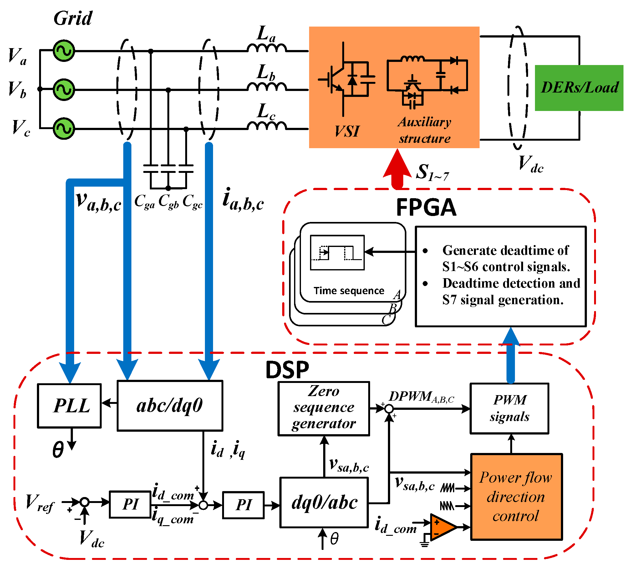
2. Proposed Bidirectional ZVS Three-Phase Converter

A bidirectional three-phase AC/DC converter is commonly used as an interface between the AC grid and distributed energy resources (DERs) and/or energy storage systems to facilitate bidirectional power flow and maintain proper AC shaping and DC voltage regulation. As a result, the performance of grid-tied bidirectional three-phase AC/DC converters has received significant attention in renewable energy systems, particularly concerning efficiency.

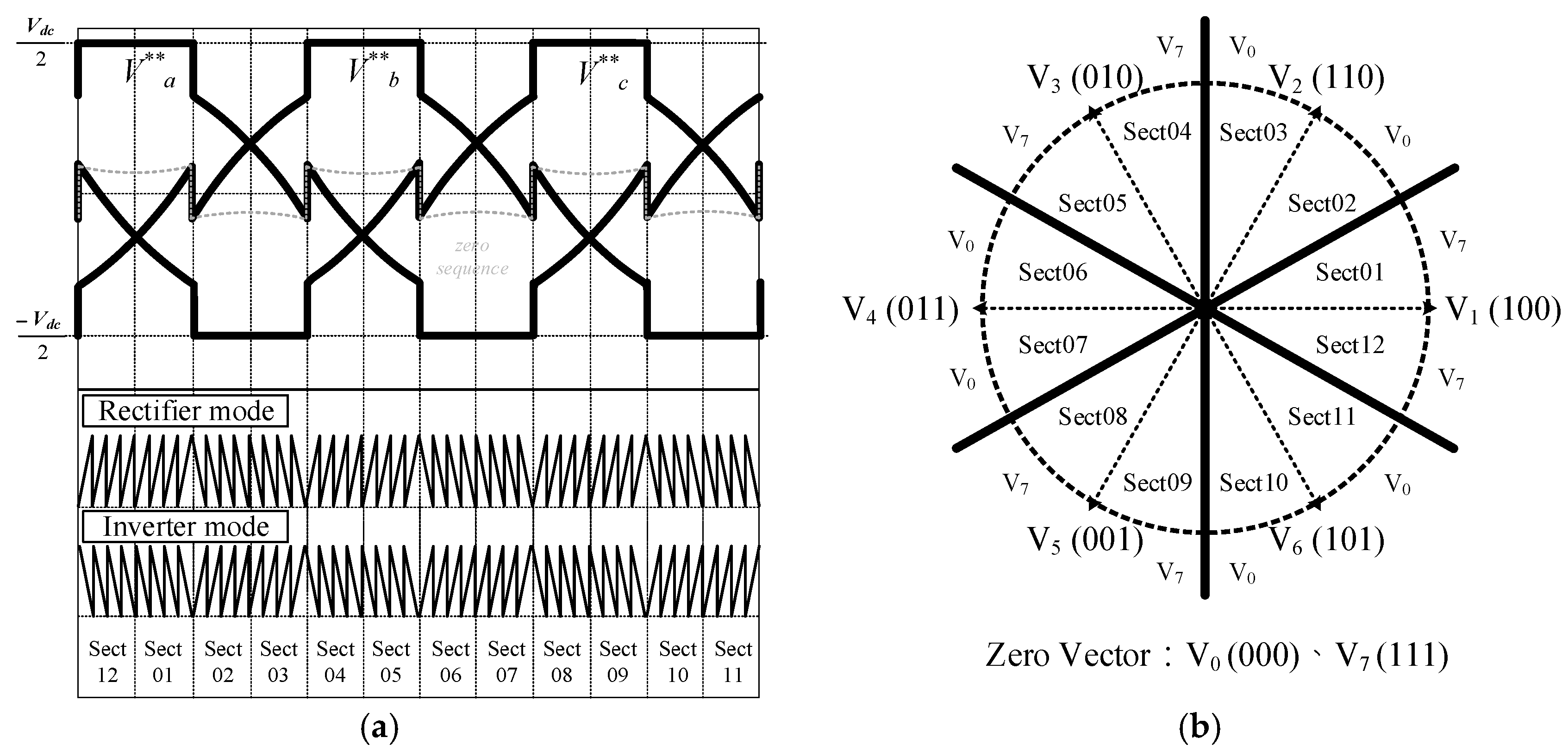
2.1. Proposed Circuit Topology and PWM Strategy

The proposed bidirectional grid-tied ZVS three-phase converter is shown in Figure 1, which is composed of a standard six-switch converter with an LC filter on the AC side and a bidirectional auxiliary resonant circuit on the DC side. In order to achieve bidirectional power flow, the voltage-oriented control (VOC) method is used to control the converter. In order to achieve soft switching, the proposed pulse-width modulation strategy ZVS DPWM shown in Figure 2 is used, where the control signals can be divided into 12 sectors during each line cycle. The positive/negative slope of the sawtooth carrier is decided using the DPWM and operation mode to generate the switching sequence and the selected zero vectors both in the rectifier mode and inverter mode, as shown in Figure 2a. While the converter is operated in the rectifier (inverter) mode and the controlled DPWM signals reach the maximum value, the slope of the sawtooth carrier is positive (negative). In contrast, when the DPWM signals reach the minimum value, the slope of the sawtooth carrier is negative (positive). While the DPWM control signal is a generalized DPWM (GDPWM) method, DPWM1 [26] was adopted in this study. By adding the zero-sequence signal to the three original modulation waves V*a, V*b and V*c, the GDPWM waves V**a, V**b and V**c are generated. Assuming |V*a| ≥ |V*b| and |V*c|, then the zero sequence signal is v0 = (sign(V*a))(Vdc/2) − V*a.
Within the proposed carrier-based control strategy, the choice of zero vectors, namely, V0 and V7, is depicted in Figure 2b. The control signal for the auxiliary switch S7 is then computed to achieve ZVS in both the main S1S6 switches and the auxiliary S7 switch during both rectifier and inverter operational modes.
  • Rectifier Mode
In the rectifier mode, the switching scheme of the carrier is illustrated in Figure 2. When the control signal is clamped at +Vdc/2, the falling sawtooth waveform is employed for that interval, whereas when the voltage clamp is set at −Vdc/2, the rising sawtooth waveform is used for that interval. Combining this with DPWM1, the switching sequence shown in Table 2 is generated. Taking interval 01 as an example for analysis, the modulation sequence of the switches is 111 → 110 → 100 → 111.
B.
Inverter Mode
For the inverter mode, the switching scheme of the carrier is depicted in Figure 2. When the voltage clamp is set at +Vdc/2, the rising sawtooth waveform is utilized for that interval, while when the voltage clamp is positioned at −Vdc/2, the falling sawtooth waveform is employed for that interval. As a result, the sawtooth waveform undergoes a transition every 60 degrees. Combining this with DPWM1, the switching sequence illustrated in Table 3 is generated. Taking interval 01 as an example for analysis, the modulation sequence of the switches is 111 → 100 → 110 → 111.
By employing the proposed DPWM strategy and the zero-vector selection illustrated in Figure 2, it becomes feasible to derive a twelve-sector switch modulation sequence within a line cycle. Take sector 1 as an example, and assume the three-phase current ia > 0 > ib > ic. For a convenient explanation of how the proposed modulation scheme works, the theoretical key waveforms during the sector 1 operation in both rectifier and inverter modes are illustrated in Figure 3 and the following assumptions are made to simplify the operation principle analysis of the bidirectional grid-tied ZVS three-phase converter.
(1)
The main switches S1S6 and auxiliary switch S7 are considered ideal switches with their anti-paralleled diodes (body diodes). The body diodes of switches S1~S7 are named D1~D7, respectively.
(2)
All of the parasitic capacitances Cr1–Cr7 are in parallel with the switches S1S7, respectively. Suppose Cr1 = Cr2 = ⋯ = Cr6.
(3)
The clamping capacitor Cc possesses a substantial capacitance, resulting in a minor voltage ripple across it. As a consequence, the voltage vCc can be treated akin to a voltage source.
(4)
The operational frequency of the converter is significantly higher than the resonant frequency of the LC filter on the AC side.
(5)
The current isx, where x belongs to the set {1, 2, …, 7}, characterizes the switch current incorporating the parasitic capacitor current. Meanwhile, the current icex, with x also within the set {1, 2, …, 7}, represents the switch current after eliminating the parasitic capacitor contribution. The voltage vcex, x∈{1, 2, …, 7}, represents the switch voltage. vcr denotes the resonant capacitor voltage.

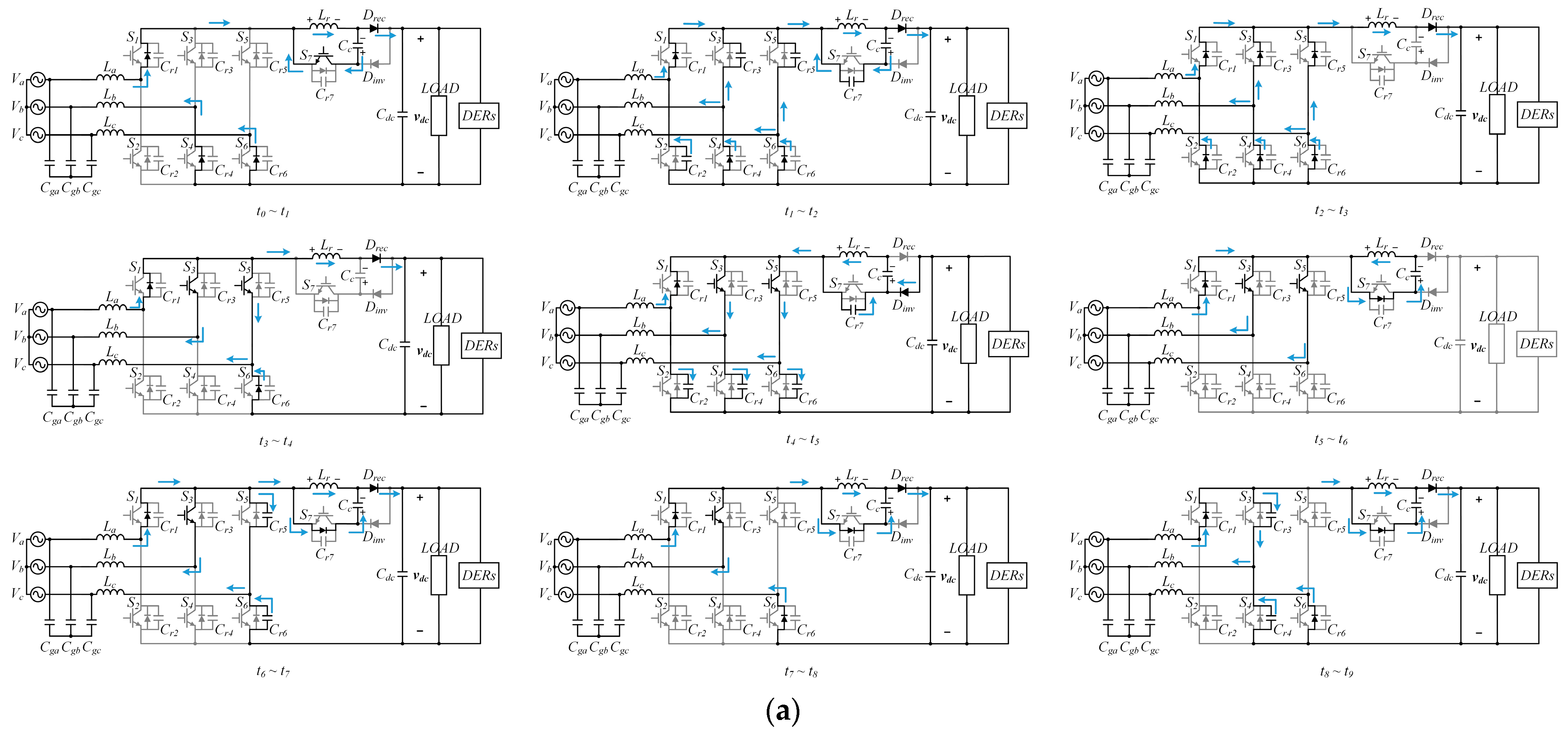
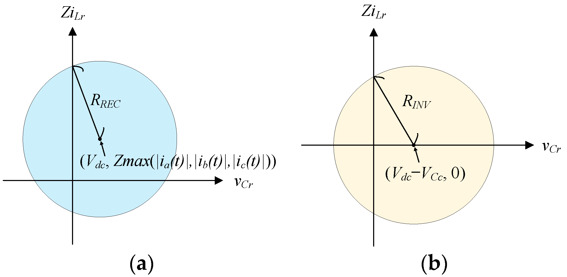
2.2. Rectifier Mode Operation

In order to understand the proposed control strategy in this topology operated in rectified mode, the steady-state key waveforms in sector 1 are shown in Figure 3a. The vector sequence during this sector is 111-110-100-111, as shown in Figure 4a. The corresponding operation state is explained as follows, and the equivalent circuit in each state is illustrated in Figure 5a.
State 1 (t0~t1): The circuit state is operated in vector V1(100). D1, D4, D6, Drec and S7 are in the conducting state; Dinv is turned off; and the resonant inductor Lr is magnetized by clamping capacitor Cc, which can be expressed by (1). The energy flows from the AC side to the DC side.
d i L r ( t ) d t = v C c L r
State 2 (t1~t2): At instant t1, S7 is turned off, and Lr resonates with Cr2, Cr3, Cr5 and Cr7. Cr2, Cr3 and Cr5 are discharged and Cr7 is charged. The energy flows from the AC side to the DC side. The state equations for Lr, Cr and CC can be expressed as shown in (2) and (3).
d i L r ( t ) d t = ( v d c v C r ( t ) ) L r
3 C r d v C r t d t + C r 7 d ( v C c + V d c v C r ( t ) ) d t = i L r t i a ( t )
State 3 (t2~t3): In this stage, the circuit state becomes vector V7(111). The voltages on Cr2, Cr3 and Cr5 drop to zero, and the body diodes on the six main switches are conducting at t2. Then, S3 and S5 are turned on via ZVS at instant t2. The diode reverse recovery current in S2 is suppressed by Lr. The voltage on Cr7 oscillates to be Vo + vCc. The energy flows from the AC side to the DC side. The state equations for Lr and Vdc can be expressed as shown in (4).
d i L r ( t ) d t = V d c L r
State 4 (t3~t4): The circuit is still operated in vector V7(111) and the body diode of switch S6 is conducting. The AC-side circuit becomes a loop. The diode reverse recovery current in S4 is suppressed by Lr. The current of Lr is charged by Vdc. The state equations for the Lr can be expressed as shown in (5).
d i L r ( t ) d t = V d c L r
State 5 (t4~t5): The circuit is still operated in vector V7(111) but the body diode of S6 is turned off. Lr resonates with Cr2, Cr4, Cr6 and Cr7. The capacitors Cr2, Cr4 and Cr6 are charged and Cr7 is discharged. The voltage of switch S7 is decreased to zero at time t5. The diode reverse recovery current in S6 is suppressed by Lr, and the energy of the inductor Lr is restored to the AC side. The diode states in the auxiliary circuit are changed. Dinv is conducting and Drec is turned off. The state equations for Lr and Cr can be expressed as shown in (6) and (7).
d i L r ( t ) d t = ( V d c v C r t v C c ) L r
3 C r d v C r t d t C r 7 d ( V d c v C r ( t ) ) d t = i L r t
State 6 (t5~t6): The circuit state is still operated in vector V7(111). S7 is turned on via ZVS at instant t5. Both Dinv and Drec are turned off. The capacitor Cc is charged by Lr, which can be described by (8).
d i L r ( t ) d t = V C c L r
State 7 (t6~t7): The circuit state becomes vector V2(110). The phase current ic is discharging Cr6 and Cr5. The Drec is conducting and Dinv is turned off. The energy flows from the AC side to the DC side. The state equation relationships between Lr, Cr and Cc can be expressed by (9) and (10).
d i L r ( t ) d t = V C c L r
i c t = C r 6 d v C r 6 t d t + C r 5 d v C r 5 t d t
State 8 (t7~t8): The circuit remains in operation within vector V2(110). The body diode of switch S6 is in a conductive state. Power continues to transfer from the AC side to the DC side. Cc is charged by Lr, which can be expressed by (11).
d i L r ( t ) d t = v C c L r
State 9 (t8~t9): The circuit state changes from vector V2(110) to vector V1(100). The phase current ib is charging Cr3 and discharging Cr4. The energy flows from the AC side to the DC side. The state equations for Lr and Cr can be expressed as shown in (12) and (13).
d i L r ( t ) d t = v C c L r
i b t = C r 4 d v C r 4 t d t + C r 3 d v C r 3 ( t ) d t

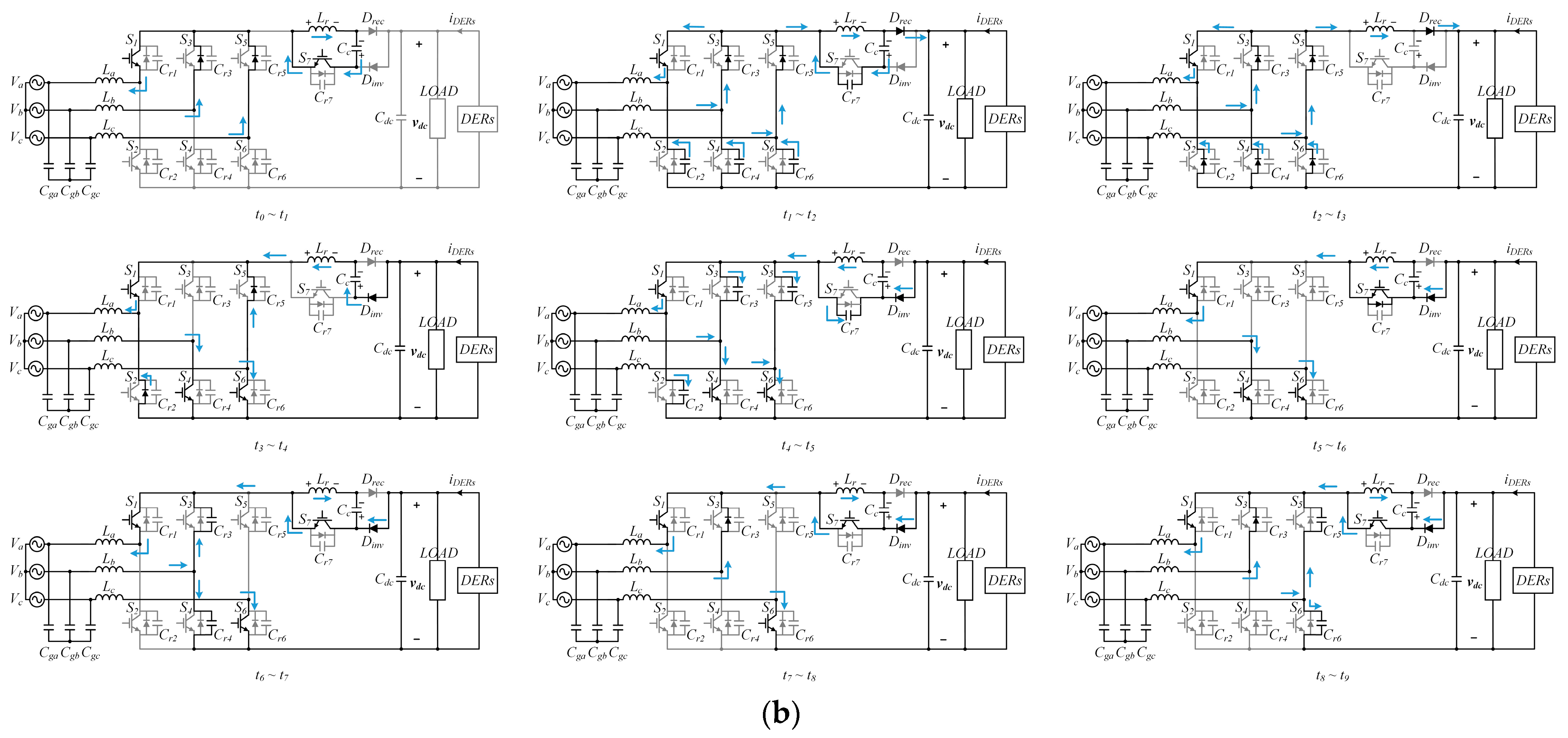
2.3. Inverter Mode Operation
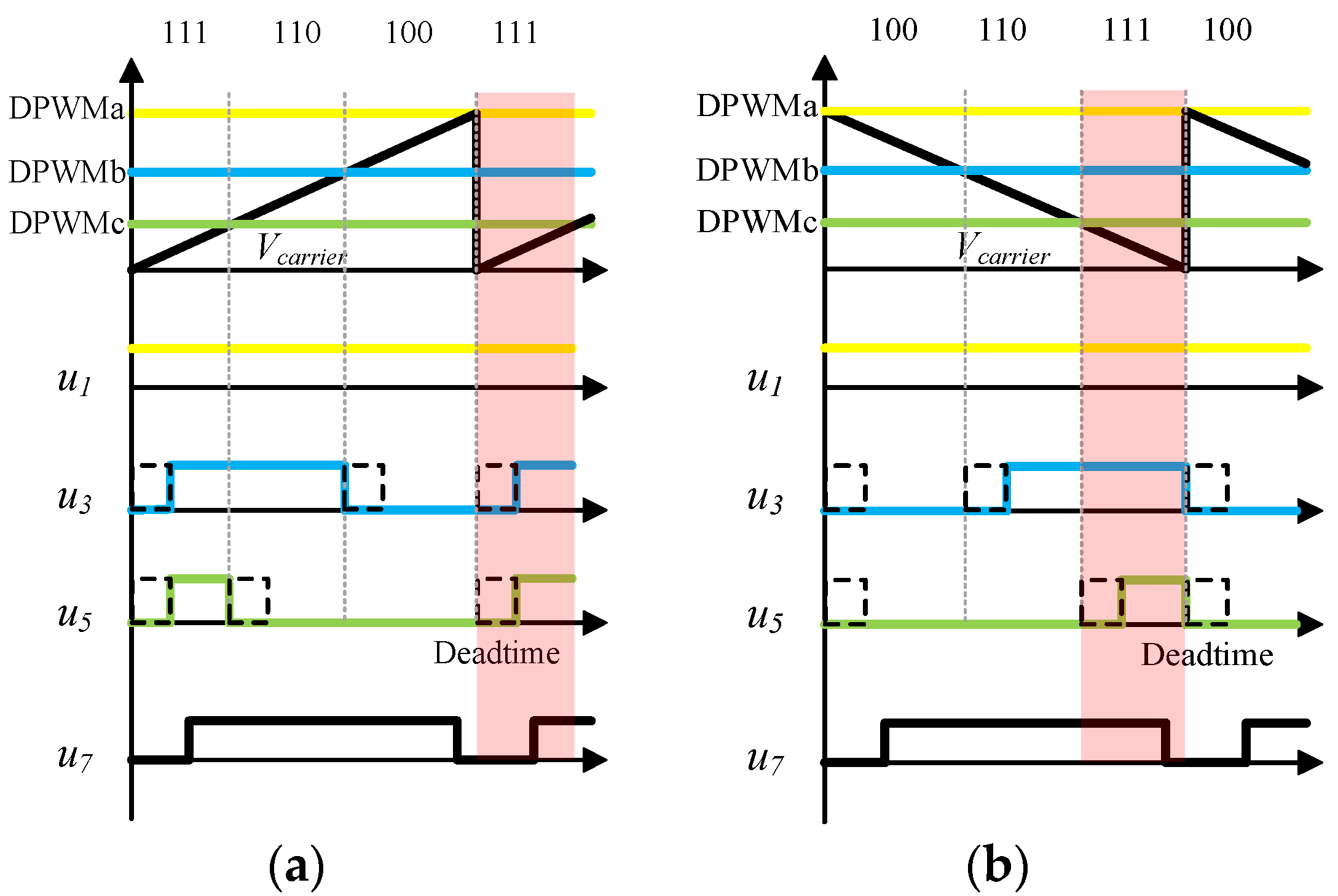
In order to understand the proposed control strategy in the proposed topology operated in inverter mode, the steady-state key waveforms in sector 1 are shown in Figure 3b. The vector sequence during this sector is 111-100-110-111, as shown in Figure 4b. The corresponding operation state is explained as follows, and the equivalent circuit in each state is illustrated in Figure 5b.
State 1 (t0~t1): The circuit functions while in vector state 111, where switch S1, auxiliary switch S7, and anti-parallel diodes D3 and D5 are on. The inverter operates under a zero-vector condition. The resonant inductor Lr is charged through the clamping voltage vCc. Dinv and Drec are turned off. The corresponding equivalent circuit is depicted in Figure 5b, and the relationship between Lr and Cc is described by (14).
d i L r ( t ) d t = v C c L r
State 2 (t1~t2): The resonant inductor Lr exhibits resonance, along with Cr2, Cr4, Cr6 and Cr7. During this state, switches S3 and S5 are turned off. Excess energy flows back to the distributed energy storage system or capacitor via Drec. Figure 5b illustrates the corresponding equivalent circuit, and the relationships between Cc, Cr and Lr can be expressed as shown in (15) and (16).
d i L r ( t ) d t = ( v C r t V d c ) L r
3 C r d v C r t d t + C r 7 d V d c v C r t v C c d t = i L r ( t )
State 3 (t2~t3): During this state, the circuit functions in vector state 100. The voltages across Cr2, Cr4 and Cr6 are discharged to zero, while the voltage across Cr7 is elevated to VDC. The anti-paralleled diodes D2, D3, D4, D5 and D6 are on. Under ZVS conditions, at time instant t2, the switches S4 and S6 are turned on, while the resonant inductor Lr mitigates the reverse recovery current in the anti-parallel diode D3. Dinv is still turned off and Drec is still turned on. Excess energy still flows back to the distributed energy storage system or capacitor via Drec. Energy recycling is achieved. Figure 5b illustrates the corresponding equivalent circuit, and the relationship between iLr and vCc is expressed by (17).
d i L r ( t ) d t = V d c L r
State 4 (t3~t4): The main switches S1, S4 and S6 are held in the on state, while the resonant inductor Lr mitigates the reverse recovery current in the anti-parallel diodes D2 and D5. Dinv is turned on and Drec is turned off. The power flow is transferred from the DC side to the AC side. The corresponding equivalent circuit is depicted in Figure 5b, and the relationship between iLr and vCc is formulated in (18).
d i L r ( t ) d t = ( V d c v C c ) L r
State 5 (t4~t5): Resonance is established in the resonant inductor Lr in conjunction with Cr2, Cr3, Cr5 and Cr7. The anti-paralleled diode D7 prepares to turn on at t5. During this state, Cr2, Cr3 and Cr5 are charged and Cr7 is discharged. Dinv is in the on state and Drec is in the off state. The power continues to transfer from the DC side to the AC side. The corresponding equivalent circuit is depicted in Figure 5b, and the relationships between iLr, vcr and vCc is described in (19) and (20).
d i L r ( t ) d t = V C c V d c + v C r ( t ) L r
3 C r d v C r ( t ) d t + i a t = C r 7 d V d c v C r t d t i L r ( t )
State 6 (t5~t6): At this time, the circuit remains functional in vector state 100, with the main switches S1, S4 and S6 in the on state. The auxiliary switch S7 is turned on under the ZVS condition. The voltage across the clamping capacitor vCc is charged through the resonant inductor current iLr. Dinv is conducting, Drec is non-conducting and power is directed from the DC side to the AC side. The equivalent circuit is depicted in Figure 5b, and the relationship between iLr and vCc is expressed in (21).
d i L r ( t ) d t = v C c L r
State 7 (t6~t7): At this time, the circuit functions in vector state 100. The current in phase ib results in the discharge of voltage across vCr3 while simultaneously charging the voltage across vCr4. Dinv is conducting, while Drec remains non-conductive, allowing power to transition from the DC side to the AC side. The equivalent circuit is illustrated in Figure 5b, and the relationships between vCr3, vCr4 and iLr are shown in (22) and (23).
d i L r ( t ) d t = v C c L r
i b t = C r 3 d v C r 3 t d t + C r 4 d v C r 4 ( t ) d t
State 8 (t7~t8): During this state, the circuit operates in vector state 110. The main switches S1 and S6, alongside the auxiliary switch S7 and the anti-parallel diode D3, are concurrently conducting. Dinv is in the on state and Drec is in the off state. Power continues to transfer from the DC side to the AC side. The corresponding equivalent circuit is displayed in Figure 5b, and the relationship between iLr and vCc is shown in (24).
d i L r ( t ) d t = v C c L r
State 9 (t8~t9): During this state, the circuit remains in operation within vector state 110. The phase current ic leads to the depletion of voltage across vCr5, while simultaneously charging the voltage across vCr6. Dinv is in the on state and Drec is in the off state, allowing power transfer from the DC side to the AC side. The depicted equivalent circuit is illustrated in Figure 5b. Subsequent to this state, the circuit’s operation reverts to the initial stage, commencing a new cycle. The relationships between the voltage and current across the inductor and capacitor are shown in (25) and (26).
d i L r ( t ) d t = v C c L r
i c t = C r 5 d V C r 5 t d t + C r 6 d v C r 6 ( t ) d t

2.4. Control Scheme

In order to control the bidirectional grid-tied three-phase converter via ZVS with the proposed modulation scheme, the control block shown in Figure 6 is used. Based on the voltage-oriented control scheme, the AC grid voltages, the DC DERs/load voltage, and AC-side currents are sensed and fed into the A/D converters, and then the phase lock loop (PLL) is utilized to synchronize the AC grid voltage. Thus, the control signals in the abc nature reference frame are transformed into the d-q synchronous reference frame. To achieve the bidirectional power flow control, the d-axis current command is utilized to judge the power flow direction (PFD) and generate the corresponding DPWM modulation control scheme and main and auxiliary switch control signals to achieve zero-voltage switching, both in the rectifier and inverter operations. Meanwhile, the reverse recovery currents of body diodes in the main switches are also suppressed.

2.5. Circuit Design

To achieve zero-voltage switching in a bidirectional grid-tied three-phase converter, the state-plane trajectory is considered to design the inductor and capacitor of the proposed circuit.
Considering the system operated at the state 2 (t1~t2) in sector 1 under the rectifier mode and according to Equations (2) and (3), one can obtain
v C r ( t ) = V d c + V C c cos ω t Z ( i L r . max i a ) sin ω t i L r ( t ) = i a + 1 Z V C c sin ω t + ( i L r . max i a ) cos ω t
where Z is the characteristic impedance, which is defined as
Z = L r / ( 3 C r + C r 7 )
While all the sectors 1–12 are considered in the rectifier mode operated in state 2 (t1~t2), the generalized circuit expression can be derived:
{ L r d i L r ( t ) d t = V d c + v C r ( t ) C r d v C r ( t ) d t = i L r ( t ) max ( | i a | , | i b | , | i c | )
Then, the generalized solution for the ZVS rectifier resonant circuit can be expressed as follows
{ v C r ( t ) = V d c + V C c cos ω t Z ( i L r . max max ( | i a | , | i b | , | i c | ) ) sin ω t i L r ( t ) = max ( | i a | , | i b | , | i c | ) + 1 Z V C c sin ω t + ( i L r . max max ( | i a | , | i b | , | i c | ) ) cos ω t
According to (30), the ZVS rectifier resonant circle can be illustrated in Figure 7a, where RREC is the radius of the ZVS rectifier resonant circle.
R R E C = V C c 2 + ( Z ( i L r . max max ( | i a | , | i b | , | i c | ) ) ) 2
Similarly, considering the system operated under the inverter mode at the state 2 (t1~t2) for sectors 1–12, the generalized circuit expression also can be derived as follows:
{ v C r ( t ) = V d c V C c + V C c cos ω t Z i L r . max sin ω t i L r ( t ) = 1 Z V C c sin ω t + i L r . max cos ω t
According to (32), the ZVS inverter resonant circle can be illustrated in Figure 7b, where RINV is the radius of the ZVS inverter resonant circle.
R I N V = V C c 2 + ( Z i L r . max ) 2
In order to achieve the zero-voltage switching function, the radii of the ZVS rectifier and ZVS inverter must be greater than Vdc and VdcVCc, respectively. Therefore, the following equations must be satisfied.
In the ZVS rectifier:
V C c 2 + ( Z ( i L r , max max ( | i a ( t ) | , | i b ( t ) | , | i c ( t ) | ) ) ) 2 > V d c
In the ZVS inverter:
V C c 2 + ( Z i L r , max ) 2 > V d c V C c
For a convenient design, (34) and (35) can be simplified as follows:
In the ZVS rectifier:
Z 2 > V d c 2 V C c 2 ( i L r , max max ( | i a ( t ) | , | i b ( t ) | , | i c ( t ) | ) ) 2 V d c 2 V C c 2 Δ i L r , R E C 2
In the ZVS inverter:
Z 2 > ( V d c V c c ) 2 V C c 2 ( i L r , max ) 2 ( V d c V c c ) 2 V C c 2 Δ i L r , I N V 2
where ΔiLr,REC and ΔiLr,INV are half of the peak-to-peak inductor current ripples.
Hence, to accomplish the ZVS bidirectional converter, one can choose a proper capacitor CC and then the resonant inductor Lr must satisfy both (36) and (37) to achieve Vcr = 0, as shown in Figure 7, before the switches are turned on.

2.6. Controller Design

In order to achieve bidirectional power flow control with ZVS, a dynamic model is needed. Because the auxiliary circuit is operated during the original switching time of the main six switches, there is no influence on the control of the original six-switch converter. Therefore, the dynamic model of the proposed converter in the d-q frame is
v d = R i d + L d i d d t ω L i q + S d v d c
v q = R i q + L d i q d t + ω L i d + S q v d c
C d c d v d c d t = i d S d + S q i q i d c
where R is the equivalent series resistance on the grid side. v d and v q are the d-axis and q-axis grid voltages in the synchronous frame, respectively. The i d and i q are the d-axis and q-axis grid currents in the synchronous frame, respectively. Sd and Sq are the state-averaged control signals in the d-q frame.
Since the DC output power is only contributed to by the i d current and the i q current is negligible, (40) can be rewritten as
C d c d v d c d t = K P v v d c * v d c + K I v v d c * v d c d t S d v d c R L
where R L is the DC side load. K P v and K I v are the DC bus voltage proportional–integral (PI) compensators. Differentiating (41) with respect to time yields
C d c v d c ¨ = K P v v d c * ˙ v d c ˙ + K I v v d c * v d c S d v d c ˙ R L
Applying the Laplace transform to (42), the outer voltage loop transfer function gives
v d c v d c * = K P v s + K I v S d C d c s 2 + K P v S d + 1 R L C d c s + K I v S d C d c
Therefore, the PI compensator K P v and K I v of the outer voltage control loop can be designed according to (43).
Next, consider the inner current control loop. In (38) and (39), the decoupled terms ω L i d and ω L i q can be directly added into the d-q control frame, and thus, S d and S q have no coupled terms. Therefore, S d and S q can be expressed as
S d = K P d i i d * i d + K I d i i d * i d d t
S q = K P q i i q * i q + K I q i i q * i q d t
where K P d i , K I d i and K P q i , K I q i are the d-axis and q-axis PI compensators of the inner current control loop, respectively. Assume the amplitude of the input voltage is constant. Differentiating (38) and (39) with respect to time yields
0 = R i d ˙ + L i d ¨ + K P d i i d * ˙ i d ˙ + K I d i i d * i d v d c
0 = R i q ˙ + L i q ¨ + K P q i i q * ˙ i q ˙ + K I q i i q * i q v d c
Applying the Laplace transform to (46) and (47), the inner current-loop transfer functions for d-axis and q-axis gives
i d i d * = s K P d i + K I d i v d c L s 2 + R K P d i v d c L s K I d i v d c L
i q i q * = s K P q i + K I q i v d c L s 2 + R K P q i v d c L s K I q i v d c L
The PI compensator of the inner current control loop can be derived by the linear time-invariant dynamic model (48) and (49). It is also important to note that the bandwidth of the inner current loop must be broader than that of the outer voltage loop.

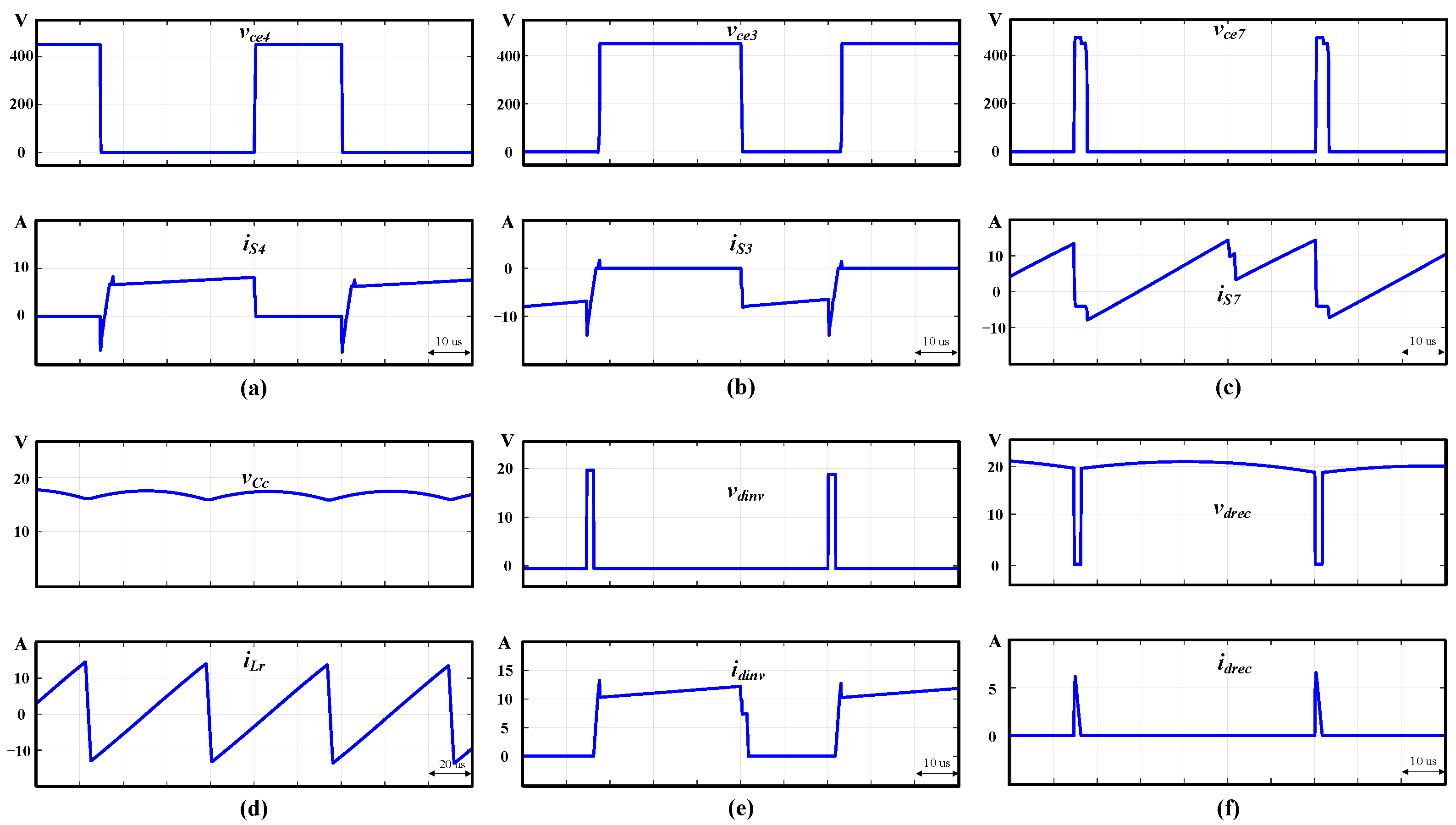
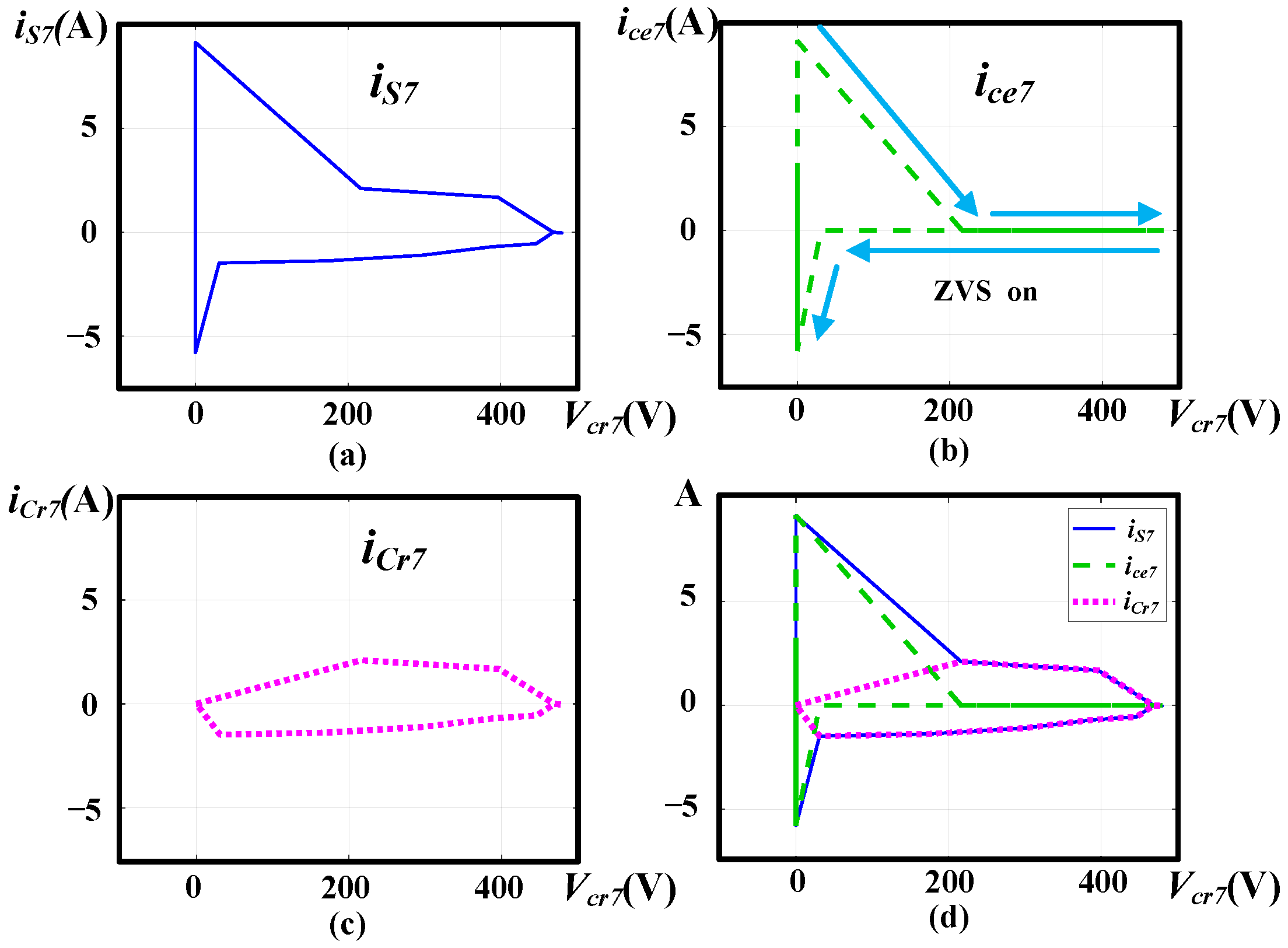
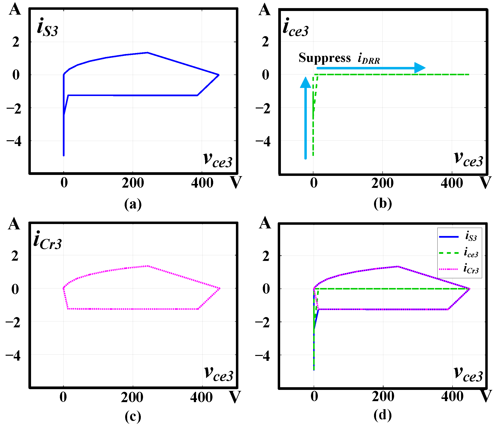
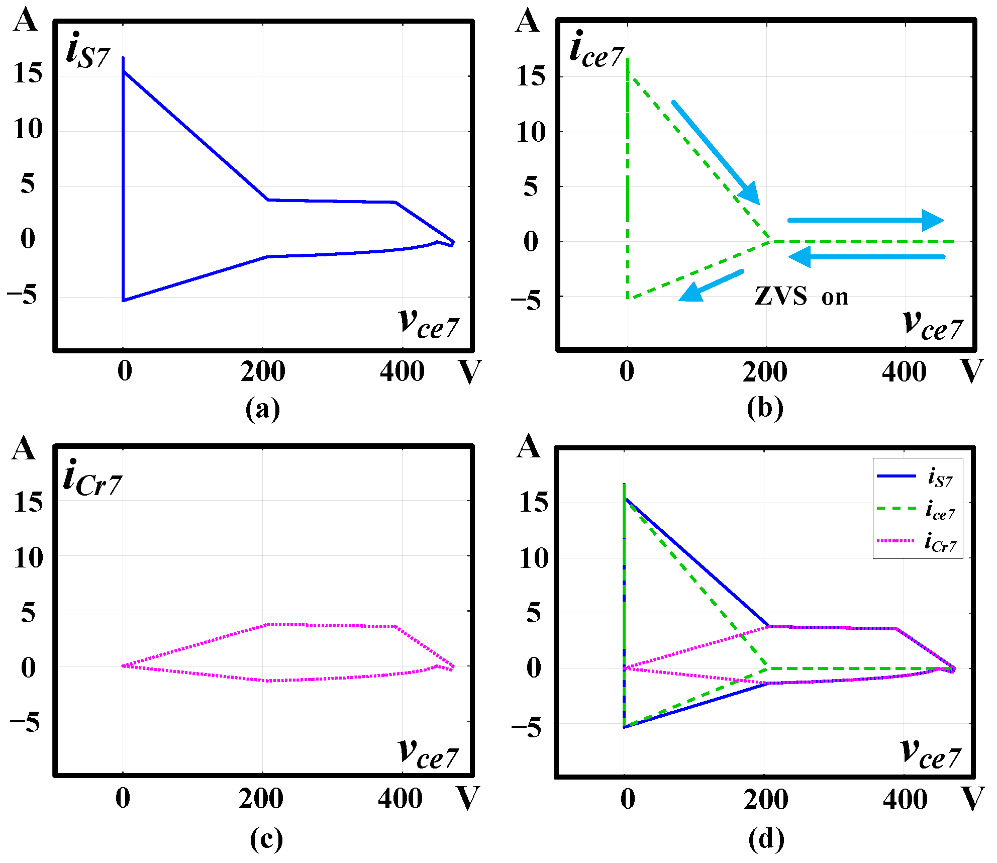
3. Simulation Results

In order to verify the validity of the proposed circuit topology and corresponding modulation strategy, the simulation software Power SIM Version 9.1.1.400 was adopted and the simulation was conducted using the system parameters listed in Table 4 according to the circuit design in Section 2.5. The parameters that were designed and selected could cause both the main and auxiliary switches to achieve soft switching, and the body diode reverse recovery current suppressed by inductor Lr. In this implementation, the IGBT FUJI 2MBI100VA-120-50 was utilized as the power switch. Therefore, a simulated parasitic capacitor Cr = 2 nF, resonant inductor Lr = 40 uH and clamping capacitor Cc = 100 μF were selected.
First, consider the proposed bidirectional grid-tied ZVS three-phase converter that was operated in the rectifier mode. The simulation waveforms of the switch voltage and current for the main switches S3 and S4 are shown in Figure 8a and Figure 8b, respectively. As can be observed from Figure 8a,b, S3 was turned on under the ZVS condition, and the diode reverse recovery current in S4 could be suppressed when S4 was turned off. Figure 8c shows the voltage and current waveforms of auxiliary switch S7, and one can find that S7 was turned on under the ZVS condition. The voltage of the clamping capacitor vCc and the current of the resonant inductor iLr are shown in Figure 8d. As can be seen from Figure 8d, vCc was much smaller than Vdc such that the voltage stress on the main and auxiliary switches was vcc + VdcVdc. Figure 8e,f show the voltage and current waveforms of diodes Dinv and Drec, respectively. It follows from Figure 8e,f that the diode voltage stress vCc was much smaller than Vdc.
Next, consider the proposed bidirectional grid-tied ZVS three-phase converter that was operated in the inverter mode. The simulation waveforms of switch voltage and current for the main switches S4 and S3 are shown in Figure 9a and Figure 9b, respectively. As can be observed from Figure 9a,b, S4 was turned on under the ZVS condition, and the diode reverse recovery current in S3 could be suppressed when S3 was turned off. Figure 9c shows the voltage and current waveforms of auxiliary switch S7, and it can be seen from Figure 9c that S7 was turned on under the ZVS condition. The voltage of the clamping capacitor vCc and the current of the resonant inductor iLr are shown in Figure 9d. It follows from Figure 9d that vCc was much smaller than Vdc such that the voltage stress on the main and auxiliary switches was vcc + VdcVdc. The voltage and current waveforms of diodes Dinv and Drec are shown in Figure 9e and Figure 9f, respectively. As can be observed from Figure 9e,f, the diode voltage stress was vCc, which was the same as that in the rectifier mode and was much smaller than Vdc.
In order to gain further insight into the operation of zero-voltage switching and the suppression of the reverse-recovery current in the proposed bidirectional grid-tied ZVS three-phase converter, the simulation process was carried out when the system was operated in both rectifier and inverter modes. The simulated ZVS process of switch S3 in the rectifier mode is shown in Figure 10. It should be noted that the switch current isx, x∈{1, 2, …, 7}, was defined as isx = icex + icrx, which includes the parasitic capacitor current icrx, but the switch current icex did not include the parasitic capacitor current icrx. The plots of is3 versus vce3, ice3 versus vce3 and icr3 versus vce3 are shown in Figure 10a, Figure 10b and Figure 10c, respectively. Figure 10d shows the overlap plot of Figure 10a–c. As can be observed from Figure 10, the ZVS on was indeed achieved in the main switch S3 in the rectifier mode. The simulated reverse-recovery-current suppression of switch S4 in the rectifier mode is shown in Figure 11. The plots of is4 versus vce4, ice4 versus vce4 and icr4 versus vce4 are shown in the Figure 11a, Figure 11b and Figure 11c, respectively. Figure 11d shows the overlap plot of Figure 11a–c. As can be seen from Figure 11, the suppression of the diode reverse-recovery process of switch S4 was indeed completed in the rectifier mode. The plots of is7 versus vce7, ice7 versus vce7 and icr7 versus vce7 are shown in the Figure 12a, Figure 12b and Figure 12c, respectively. Figure 12d shows the overlap plot of Figure 12a–c. It follows from Figure 12 that the ZVS on was indeed achieved in the auxiliary switch S7 in the rectifier mode.
Similarly, the process of the ZVS operation and reverse-recovery-current suppression in the proposed bidirectional grid-tied ZVS three-phase converter operated in inverter mode are shown in Figure 13, Figure 14 and Figure 15. As can be observed from Figure 13, Figure 14 and Figure 15, the ZVS on of main switch S4, the reverse-recovery-current suppression of main switch S3 and the ZVS on of auxiliary switch S7 were indeed achieved in the inverter mode.
The simulated waveforms of the DC bus voltage Vdc, phase-a voltage Va and current ia of the proposed bidirectional grid-tied ZVS converter operated in rectifier mode and inverter mode are shown in Figure 16a and Figure 16b, respectively. As can be seen from Figure 16, when the system was operated in the rectifier mode, the controlled grid-side current was in phase with the grid voltage, and when the system was operated in the inverter mode, the controlled grid-side current was phase-shifted by 180 degrees from the grid voltage.
According to the above simulation results, the proposed circuit topology and corresponding PWM control scheme could accomplish zero-voltage switching in the main switches and the auxiliary switch in both the rectifier and inverter modes. Meanwhile, the reverse recovery current of body diodes in the main switches was also suppressed.

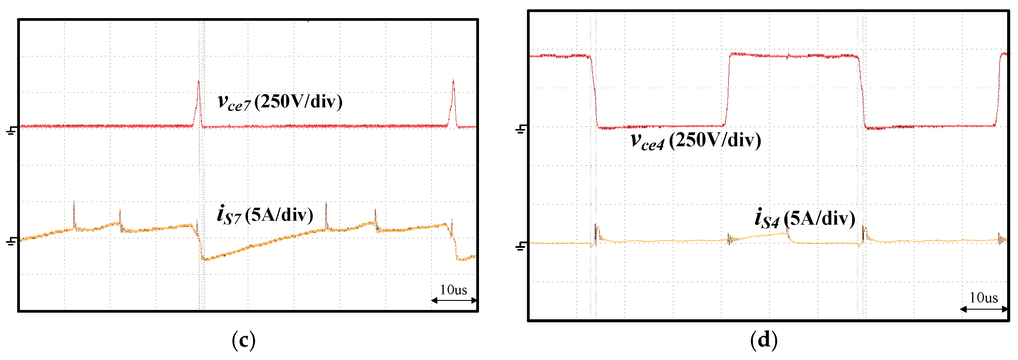
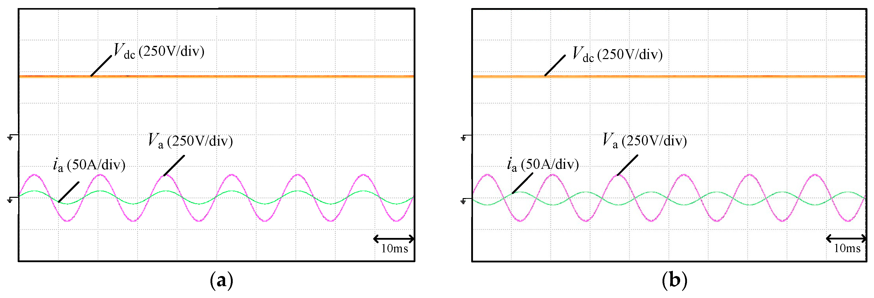
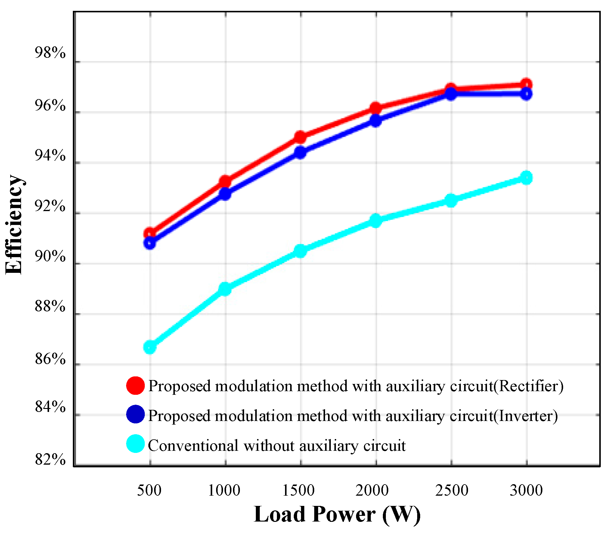
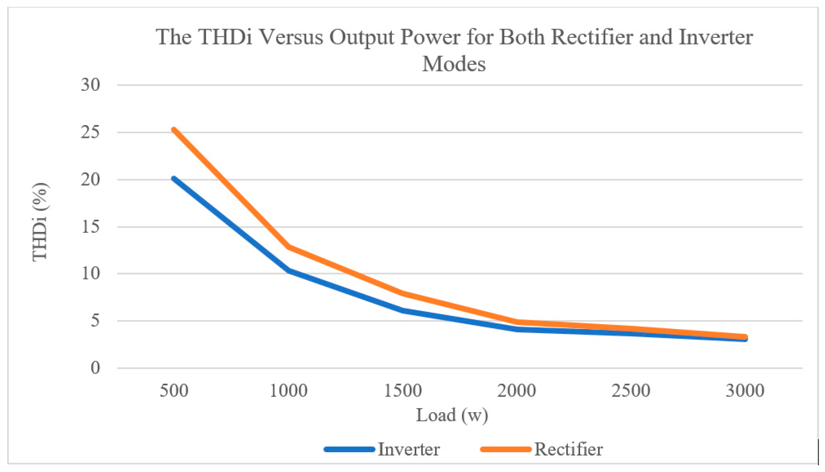
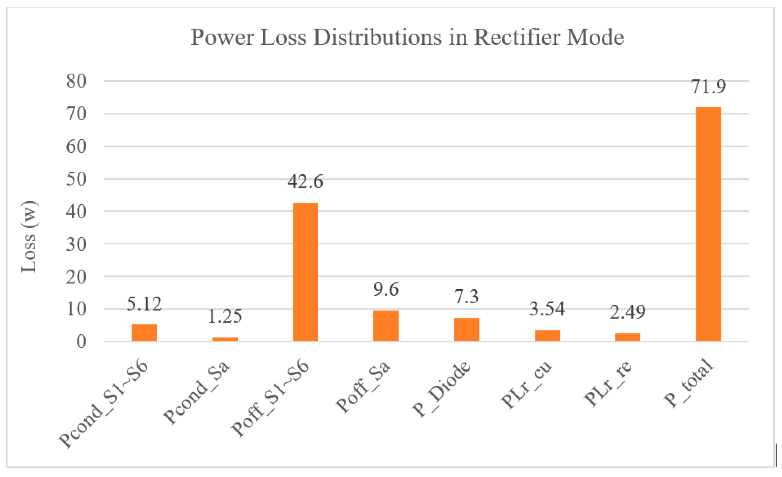
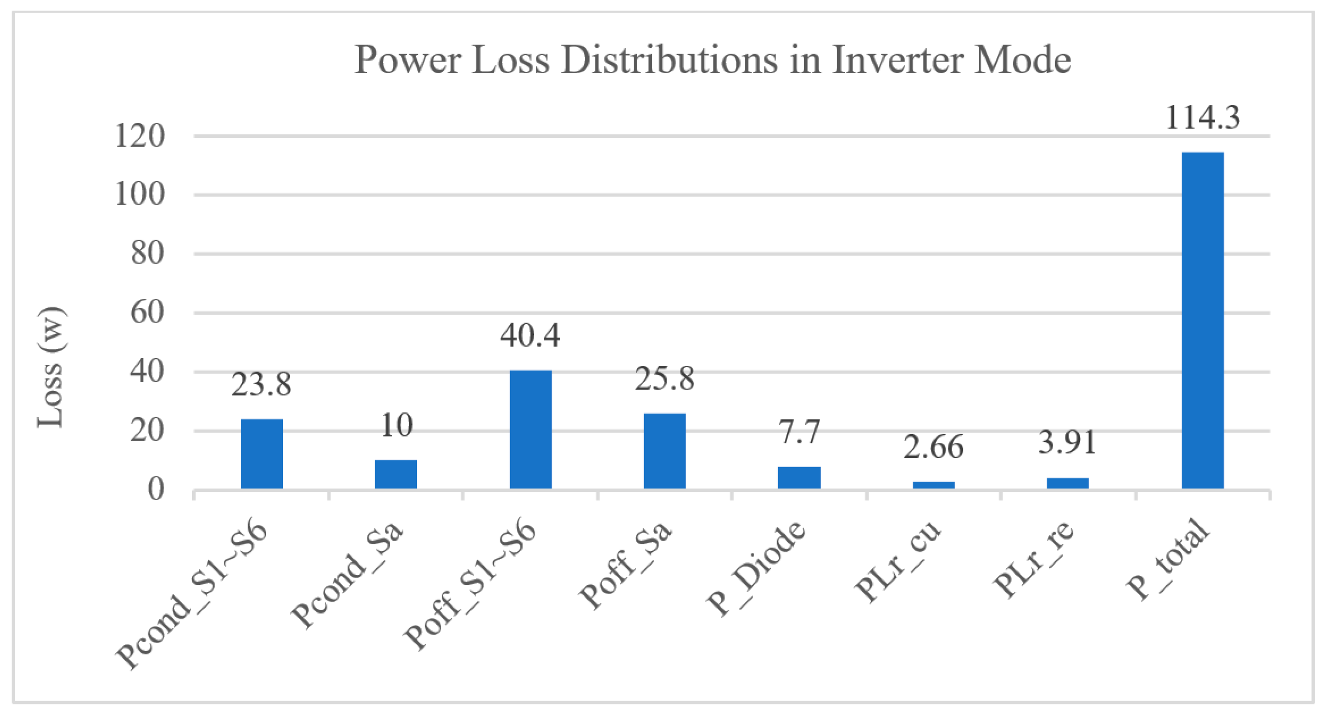
4. Experimental Results

To facilitate the understanding of the proposed circuit topology and corresponding modulation control strategy, as well as provide verification, a prototype system was constructed with the parameters listed in Table 4. The adopted active switches were the insulated gate bipolar transistors (FUJI 2MBI100VA-120-50) with a parasitic capacitance Cr = 2 nF, and the system controller was implemented with DSP TMS320F28335/FPGA Cmod-A7-35T.
Figure 17 and Figure 18 show the experimental waveforms when the proposed circuit was operated in the rectifier mode and inverter mode, respectively. While the system was operated in the rectifier mode, the measured switch voltage and current of switches S3, S4 and S7 are shown in Figure 17a–c, respectively. As can be seen from Figure 17a–c, the main switch S3 and auxiliary switch S7 were turned on via ZVS, and the diode reverse recovery current of main switch S4 was also suppressed when the system was operated in the rectifier mode. The voltage vCc of the clamping capacitor and the current iLr of the resonant inductor are shown in Figure 17d. It follows from Figure 17d that vCc was much smaller than Vdc such that the voltage stress on the main and auxiliary switches was vcc + VdcVdc. The voltage and current waveforms of diodes Dinv and Drec are shown in Figure 17e and Figure 17f, respectively. As can be observed from Figure 17e,f, the diode voltage stress is vCc. It should be noticed that the experimental waveforms of diode voltage and current in Figure 17e,f are in close agreement with the simulation waveforms in Figure 8e,f. The voltage across the two series diodes was vCc = vdinv + vdrec.
While the system was operated in the inverter mode, the measured switch voltage and current of switches S4, S3 and S7 are shown in Figure 18a–c, respectively. As can be seen from Figure 18a–c, the main switch S4 and auxiliary switch S7 were turned on via ZVS, and the diode reverse recovery current of main switch S3 was also suppressed. The voltage vCc of the clamping capacitor and the current iLr of the resonant inductor are shown in Figure 18d. It follows from Figure 18d that vCc was much smaller than Vdc such that the voltage stress on the main and auxiliary switches was vcc + VdcVdc. In addition, the voltage and current waveforms of diodes Dinv and Drec are shown in Figure 18e and Figure 18f, respectively. It follows from Figure 18e,f that the diode voltage stress was vCc, and the total voltage across the two series diodes was vCc = vdinv + vdrec.
In addition, the light load condition of 300 W for 10% of the rated output power was considered. The rectifier and inverter operations are shown in Figure 19a,b and Figure 19c,d, respectively. As can be observed from Figure 19a,b, the auxiliary switch S7 and main switch S3 were turned on via ZCS/ZVS when the converter was operated in the rectifier mode. It follows from Figure 19c,d that the auxiliary switch S7 and main switch S4 were also turned on via ZCS/ZVS when the converter was operated in the inverter mode.
Finally, in order to understand the bidirectional power flow functionality of the proposed ZVS grid-tied three-phase converter, the measured waveforms of the DC bus voltage Vdc, phase-a voltage Va and current ia in both rectifier mode (3 kW) and inverter mode (3 kW) are depicted in Figure 20a and Figure 20b, respectively. According to the control block illustrated in Figure 6, the bidirectional power flow was achieved in the proposed grid-tied ZVS three-phase converter.
Next, the efficiency was measured using three YOKOGAWA WT310Es. Compared with the traditional hard switching SPWM without an auxiliary circuit, the measured efficiency of the proposed circuit topology and control scheme in the rectifier mode and inverter mode was 3~4% higher than that of the hard switching control scheme, which is illustrated in Figure 21. The realized prototype of the proposed system is shown in Figure 22.
Finally, the current total harmonic distortion THDi and power losses were analyzed. Figure 23 shows the THDi versus output power for both rectifier and inverter operation. As depicted in Figure 23, it is evident that the higher the output power, the lower THDi became. Next, the power loss distributions are shown in Figure 24 and Figure 25 for the rectifier mode and inverter mode, respectively. In the power loss distribution, the IGBT Semikron SKM200GB125D and diode Powerex CS240650 were adopted in the simulation software to analyze the conduction loss, turn-off loss, diode loss, copper loss and core loss. As can be seen from Figure 24 and Figure 25, the total power loss during inverter operation was higher than that during rectifier operation due to the difference in auxiliary circuit paths between the inverter and rectifier operations.

5. Conclusions

This paper proposed a bidirectional grid-tied ZVS three-phase converter topology. In addition, a zero-voltage-switching PWM strategy for a grid-connected three-phase converter is proposed. The control signal for the auxiliary switch is produced using a sawtooth carrier waveform encompassing both positive and negative gradients. This approach is utilized to attain ZVS across both the main and auxiliary switches. Furthermore, the reverse recovery currents in the anti-parallel diodes of the main switches are effectively mitigated. The operational principles of the circuit are extensively elucidated for both rectifier and inverter modes. Both simulation and experimental results verified the validity of the proposed circuit topology and the proposed ZVS DPWM strategy in the bidirectional grid-tied three-phase system. The measured efficiency of the proposed system was about 3~4% higher than that of a conventional SPWM hard-switching system. It is worth mentioning that the soft switching strategies usually suffer from high voltage and current stress of the semiconductors, which will decrease the power rating of the original design. The proposed topology and PWM control scheme also had those limitations.

Author Contributions

Conceptualization, Y.-H.L. and F.-J.L.; methodology, Y.Z. and W.-R.L.; validation, Y.-H.L. and X.-S.H. The research article was the result of collaborative endeavors by the authors. Collectively, we contributed to tasks such as theoretical analysis, modeling, simulation, experimental work and manuscript preparation. All authors have read and agreed to the published version of the manuscript.

Funding

This research was funded by the National Science and Technology Council of Taiwan, R.O.C., grant number NSTC 112-2221-E-008-012 and NSTC 112-2218-E-008-011.

Data Availability Statement

Not applicable.

Conflicts of Interest

The authors declare no conflict of interest.

References

  1. Huang, Z.; Liu, Z.; Lee, F.C.; Li, Q. Critical-Mode-Based Soft-Switching Modulation for High-Frequency Three-Phase Bidirectional AC–DC Converters. IEEE Trans. Power Electron. 2019, 34, 3888–3898. [Google Scholar] [CrossRef]
  2. Li, R.; Ma, Z.; Xu, D. A ZVS Grid-Connected Three-Phase Inverter. IEEE Trans. Power Electron. 2012, 27, 3595–3604. [Google Scholar] [CrossRef]
  3. Bellar, M.D.; Wu, T.-S.; Tchamdjou, A.; Mahdavi, J.; Ehsani, M. A review of soft-switched dc-ac converters. IEEE Trans. Ind. Appl. 1998, 34, 847–860. [Google Scholar] [CrossRef]
  4. Nakaoka, M.; Yonemori, H.; Yurugi, K. Zero-voltage soft-switched PDM three phase AC-DC active power converter operating at unity power factor and sinewave line current. In Proceedings of the IEEE Power Electronics Specialist Conference, Seattle, WA, USA, 20–24 June 1993; pp. 787–794. [Google Scholar]
  5. Yonemori, H.; Fukuda, H.; Nakaoka, M. Advanced three-phase ZVS-PWM active power rectifier with new resonant DC link and its digital control scheme. In Proceedings of the Fifth International Conference on Power Electronics and Variable-Speed Drives, London, UK, 26–28 October 1994; pp. 608–613. [Google Scholar]
  6. Mao, H.; Lee, C.Y.; Boroyevich, D.; Hiti, S. Review of high performance three-phase power-factor correction circuits. IEEE Trans. Ind. Electron. 1997, 44, 437–446. [Google Scholar]
  7. Xu, D.; Feng, B.; Li, R.; Mino, K.; Umida, H. A Zero Voltage Switching SVM (ZVS–SVM) Controlled Three-Phase Boost Rectifier. IEEE Trans. Power Electron. 2007, 22, 978–986. [Google Scholar] [CrossRef]
  8. Li, R.; Ma, K.; Xu, D. A Novel Minimum Voltage Active Clamping SVM (MVAC-SVM) Controlled Three-Phase PFC. In Proceedings of the Twenty-Fourth Annual IEEE Applied Power Electronics Conference and Exposition, Washington, DC, USA, 15–19 February 2009; pp. 1879–1885. [Google Scholar]
  9. Divan, D.M. The resonant dc link converter—A new concept in static power conversion. IEEE Trans. Ind. Appl. 1989, 25, 317–325. [Google Scholar] [CrossRef]
  10. Divan, D.M.; Skibinski, G. Zero-switching-loss inverters for high power applications. IEEE Trans. Ind. Appl. 1989, 25, 634–643. [Google Scholar] [CrossRef]
  11. Venkataramanan, G.; Divan, D.M. Pulse width modulation with resonant DC link converters. In Proceedings of the IEEE Industry Applications Society Annual Meeting, Seattle, WA, USA, 7–12 October 1990; Volume 2, pp. 984–990. [Google Scholar]
  12. He, J.; Mohan, N. Parallel resonant DC link circuit-a novel zero switching loss topology with minimum voltage stresses. IEEE Trans. Power Electron. 1991, 6, 687–694. [Google Scholar] [CrossRef]
  13. Chen, Y.-T. A new quasi-parallel resonant DC link for soft-switching PWM inverters. IEEE Trans. Power Electron. 1998, 13, 427–435. [Google Scholar] [CrossRef]
  14. Jafar, J.J.; Fernandes, B.G. A new quasi-resonant DC-link PWM inverter using single switch for soft switching. IEEE Trans. Power Electron. 2002, 17, 1010–1016. [Google Scholar] [CrossRef]
  15. Mezaroba, M.; Martins, D.C.; Barbi, I. A ZVS PWM Half-Bridge Voltage Source Inverter with Active Clamping. IEEE Trans. Ind. Electron. 2007, 54, 2665–2672. [Google Scholar] [CrossRef]
  16. Gurunathan, R.; Bhat, A.K.S. Zero-Voltage Switching DC Link Single-Phase Pulsewidth-Modulated Voltage Source Inverter. IEEE Trans. Power Electron. 2007, 22, 1610–1618. [Google Scholar] [CrossRef]
  17. Li, R.; Xu, D. A Zero-Voltage Switching Three-Phase Inverter. IEEE Trans. Power Electron. 2014, 29, 1200–1210. [Google Scholar]
  18. Du, C.; Xu, D.; He, N.; Zhu, N. Modeling and Optimization of a Zero-Voltage Switching Inverter for High Efficiency and Miniaturization. IEEE Trans. Power Electron. 2017, 32, 150–163. [Google Scholar] [CrossRef]
  19. Shi, K.; Deng, J.; Xu, D. A General Pulse Width Modulation Method for Zero-Voltage-Switching Active-clamping Three- phase Power Converters: Edge Aligned Pulse Width Modulation (EA-PWM). IEEE Open J. Power Electron. 2020, 1, 250–259. [Google Scholar] [CrossRef]
  20. Wu, Y.; He, N.; Chen, M.; Xu, D. Generalized Space-Vector-Modulation Method for Soft-Switching Three-Phase Inverters. IEEE Trans. Power Electron. 2021, 36, 6030–6045. [Google Scholar] [CrossRef]
  21. He, N.; Zhu, Y.; Zhao, A.; Xu, D. Zero-Voltage-Switching Sinusoidal Pulsewidth Modulation Method for Three-Phase Four-Wire Inverter. IEEE Trans. Power Electron. 2019, 34, 7192–7205. [Google Scholar] [CrossRef]
  22. Chen, J.; Sha, D.; Zhang, J. Current Ripple Prediction and DPWM-Based Variable Switching Frequency Control for Full ZVS Range Three-Phase Inverter. IEEE Trans. Ind. Electron. 2021, 68, 1412–1422. [Google Scholar] [CrossRef]
  23. Fan, B.; Wang, Q.; Burgos, R.; Ismail, A.; Boroyevich, D. Adaptive Hysteresis Current Based ZVS Modulation and Voltage Gain Compensation for High-Frequency Three-Phase Converters. IEEE Trans. Power Electron. 2021, 36, 1143–1156. [Google Scholar] [CrossRef]
  24. Chen, J.; Han, Y.; Han, Q.; Liu, Q. A DPWM-Based Quasi-Constant Switching Frequency Control for Full ZVS Range Three-Phase Inverter with Reactive Power Transfer Capability. IEEE Trans. Ind. Electron. 2022, 70, 4912–4921. [Google Scholar] [CrossRef]
  25. Bagawade, S.; Pahlevani, M.; Jain, P. Novel Soft-Switched Three-Phase Inverter with Output Current Ripple Cancellation. IEEE Trans. Power Electron. 2023, 38, 1232–1248. [Google Scholar] [CrossRef]
  26. Hava, A.M.; Kerkman, R.J.; Lipo, T.A. Simple analytical and graphical methods for carrier-based PWM-VSI drives. IEEE Trans. Power Electron. 1999, 14, 49–61. [Google Scholar] [CrossRef]
Figure 1. The circuit topology of proposed bidirectional grid-tied ZVS three-phase converter.
Energies 16 06453 g001
Figure 2. Proposed DPWM strategy and carrier waveform diagram: (a) time domain illustration and (b) space vector illustration.
Energies 16 06453 g002
Figure 3. The theoretical key waveforms during the sector 1 operation in the (a) rectifier mode and (b) inverter mode.
Energies 16 06453 g003
Figure 4. The corresponding vector sequence in sector 1 in Figure 3 operated in the (a) rectifier mode and (b) inverter mode.
Energies 16 06453 g004
Figure 5. The equivalent circuit in each state of the proposed bidirectional soft-switching converter operated in the (a) rectifier mode and (b) inverter mode.
Energies 16 06453 g005aEnergies 16 06453 g005b
Figure 6. Control block of the proposed bidirectional ZVS three-phase converter.
Energies 16 06453 g006
Figure 7. The resonant circles for the (a) ZVS rectifier and (b) ZVS inverter.
Energies 16 06453 g007
Figure 8. Simulated waveforms of the proposed bidirectional soft-switching converter operating in the rectifier mode: (a) voltage and current of switch S3 (ZVS turn-on), (b) voltage and current of switch S4 (the diode reverse recovery current was suppressed), (c) voltage and current of auxiliary switch S7, (d) the clamping capacitor voltage vCc and resonant inductor current iLr, (e) voltage and current of diode Dinv, and (f) voltage and current of diode Drec.
Energies 16 06453 g008
Figure 9. Simulated waveforms of the proposed bidirectional soft-switching converter operating in the inverter mode: (a) voltage and current of switch S4 (ZVS turn-on), (b) voltage and current of switch S3 (the diode reverse recovery current was suppressed), (c) voltage and current of auxiliary switch S7, (d) the clamping capacitor voltage vCc and resonant inductor current iLr, (e) voltage and current of diode Dinv, and (f) voltage and current of diode Drec.
Energies 16 06453 g009
Figure 10. The ZVS process of switch S3: (a) switch current is3 vs. switch voltage vce3, (b) current ice3 vs. switch voltage vce3, (c) capacitor current icr3 vs. switch voltage vce3 and (d) the overlap of (ac) when the proposed bidirectional soft-switching converter was operating in the rectifier mode.
Energies 16 06453 g010
Figure 11. The process of diode reverse-recovery suppression of switch S4: (a) switch current is4 vs. switch voltage vce4, (b) current ice4 vs. switch voltage vce4, (c) capacitor current icr4 vs. switch voltage vce4 and (d) the overlap of (ac) when the proposed bidirectional soft-switching converter was operating in the rectifier mode.
Energies 16 06453 g011
Figure 12. The ZVS process of switch S7: (a) switch current is7 vs. switch voltage vce7, (b) current ice7 vs. switch voltage vce7, (c) capacitor current icr7 vs. switch voltage vce7 and (d) the overlap of (ac) when the proposed bidirectional soft-switching converter was operating in the rectifier mode.
Energies 16 06453 g012
Figure 13. The ZVS process of switch S4: (a) switch current is4 vs. switch voltage vce4, (b) current ice4 vs. switch voltage vce4, (c) capacitor current icr4 vs. switch voltage vce4 and (d) the overlap of (ac) when the proposed bidirectional soft-switching converter was operating in the inverter mode.
Energies 16 06453 g013
Figure 14. The process of diode reverse-recovery suppression of switch S3: (a) switch current is3 vs. switch voltage vce3, (b) current ice3 vs. switch voltage vce3, (c) capacitor current icr3 vs. switch voltage vce3 and (d) the overlap of (ac) when the proposed bidirectional soft-switching converter was operating in the inverter mode.
Energies 16 06453 g014
Figure 15. The ZVS process of switch S7: (a) switch current is7 vs. switch voltage vce7, (b) current ice7 vs. switch voltage vce7, (c) capacitor current icr7 vs. switch voltage vce7 and (d) the overlap of (ac) when the proposed bidirectional soft-switching converter was operating in the inverter mode.
Energies 16 06453 g015
Figure 16. Simulated waveforms of the DC-link voltage, phase-a voltage and phase-a current of the proposed bidirectional soft-switching converter operated in (a) rectifier mode and (b) inverter mode.
Energies 16 06453 g016
Figure 17. Measured waveforms of the proposed bidirectional soft-switching converter operating in the rectifier mode: (a) voltage and current of switch S3 (ZVS turn-on), (b) voltage and current of switch S4 (the diode reverse recovery current was suppressed), (c) voltage and current of auxiliary switch S7, (d) the clamping capacitor voltage vCc and resonant inductor current iLr, (e) voltage and current of diode Dinv, and (f) voltage and current of diode Drec.
Energies 16 06453 g017
Figure 18. Measured waveforms of the proposed bidirectional soft-switching converter operating in the inverter mode: (a) voltage and current of switch S4 (ZVS turn-on), (b) voltage and current of switch S3, (the diode reverse recovery current was suppressed), (c) voltage and current of auxiliary switch S7, (d) the clamping capacitor voltage vCc and resonant inductor current iLr, (e) voltage and current of diode Dinv, and (f) voltage and current of diode Drec.
Energies 16 06453 g018
Figure 19. Measured waveforms of the proposed bidirectional soft-switching converter at 300 W while (a,b) operating in the rectifier mode and (c,d) operating in the inverter mode: (a) voltage and current of auxiliary switch S7, (b) voltage and current of switch S3, (c) voltage and current of auxiliary switch S7, and (d) voltage and current of switch S4.
Energies 16 06453 g019aEnergies 16 06453 g019b
Figure 20. Measured waveforms of DC bus voltage Vdc, phase-a voltage Va and current ia of the proposed grid-tied ZVS three-phase converter operated in the (a) rectifier mode (3 kW) and (b) inverter mode (3 kW).
Energies 16 06453 g020
Figure 21. Measured efficiency of the bidirectional three-phase converter operated in hard switching SPWM without auxiliary circuit and proposed ZVS converter during rectifier and inverter modes.
Energies 16 06453 g021
Figure 22. Realized prototype of the proposed system.
Energies 16 06453 g022
Figure 23. The simulated total harmonic distortion THDi for both rectifier and inverter operations.
Energies 16 06453 g023
Figure 24. The simulated power loss distribution for rectifier operation.
Energies 16 06453 g024
Figure 25. The simulated power loss distribution for inverter operation.
Energies 16 06453 g025
Table 1. Comparisons of different ZVS methods in the three-phase converters.
StructureExtra Elements
(Structure)
Switching
Frequency (fs)
Switch Voltage Stress on Main and Auxiliary SwitchesSwitch Current Stress on Main/Auxiliary SwitchesFilter DesignBidirectional Operation
[7] RectifierLC + switch
(3ϕ/3w)
FixedVdc + VccVdcLow/LowLCNone
[8] RectifierLC + switch
(3ϕ/3w)
FixedVdcLow/HighLCNone
[2] InverterLC + switch
(3ϕ/3w)
FixedVdcLow/HighLCNone
[17] InverterLC + switch
(3ϕ/3w)
FixedVdc + VccVdcLow/LowLCNone
[19] BTBLC + switch
(3ϕ/4w)
FixedVdc + VccVdcLow/LowLCNone
[20] InverterLC + switch
(3ϕ/3w)
FixedVdc + VccVdcLow/LowLCNone
[21] InverterLC + switch
(3ϕ/4w)
FixedVdc + VccVdcLow/LowLCNone
[22] InverterNone
(3ϕ/3w)
VariableVdcHigh/XLCLNone
[1] ConverterNone
(3ϕ/3w)
VariableVdcHigh/XLCL
[23] InverterNone
(3ϕ/3 or 4w)
VariableVdcHigh/XLCLNone
[24] InverterNone
(3ϕ/3w)
Variable
(quasi-constant)
VdcHigh/XLCLNone
(inverter full ZVS range)
[25] Inverter3 passive filters
(current ripple cancellation)
(3ϕ/3w)
VariableVdcHigh/XTransformer, L and CNone
Proposed converterLC + switch + D
(3ϕ/3w)
FixedVdc + VccVdcLow/HighLC
Table 2. Switching sequence operated in the rectifier mode.
SectorVector
1111 → 110 → 100 → 111
2000 → 100 → 110 → 000
3000 → 010 → 110 → 000
4111 → 110 → 010 → 111
5111 → 011 → 010 → 111
6000 → 010 → 011 → 000
7000 → 001 → 011 → 000
8111 → 011 → 001 → 111
9111 → 101 → 001 → 111
10000 → 001 → 101 → 000
11000 → 100 → 101 → 000
12111 → 101 → 100 → 111
Table 3. Switching sequence operated in the inverter mode.
SectorVector
1111 → 100 → 110 → 111
2000 → 110 → 100 → 000
3000 → 110 → 010 → 000
4111 → 010 → 110 → 111
5111 → 010 → 011 → 111
6000 → 011 → 010 → 000
7000 → 011 → 001 → 000
8111 → 001 → 011 → 111
9111 → 001 → 101 → 111
10000 → 101 → 001 → 000
11000 → 101 → 100 → 000
12111 → 100 → 101 → 111
Table 4. Simulation and experimental parameters of the proposed bidirectional ZVS three-phase converter.
ParametersValueUnit
AC grid line voltage (rms)220V
DC link voltage, Vdc450V
Switching frequency, fs18kHz
Three-phase inductors, La,b,c2mH
Three-phase capacitors Cga,b,c22μF
DC-link capacitor, Cdc2200μF
Parasitic capacitance, Cr2nF
Resonant inductor, Lr40μH
Clamping capacitor, Cc100μF
Power rating, Prate3kW
Disclaimer/Publisher’s Note: The statements, opinions and data contained in all publications are solely those of the individual author(s) and contributor(s) and not of MDPI and/or the editor(s). MDPI and/or the editor(s) disclaim responsibility for any injury to people or property resulting from any ideas, methods, instructions or products referred to in the content.

