
Deep Level Transient Fourier Spectroscopy Investigation of Electron Traps on AlGaN/GaN-on-Si Power Diodes
 , ,
, ,  , , , , and
Abstract
:1. Introduction
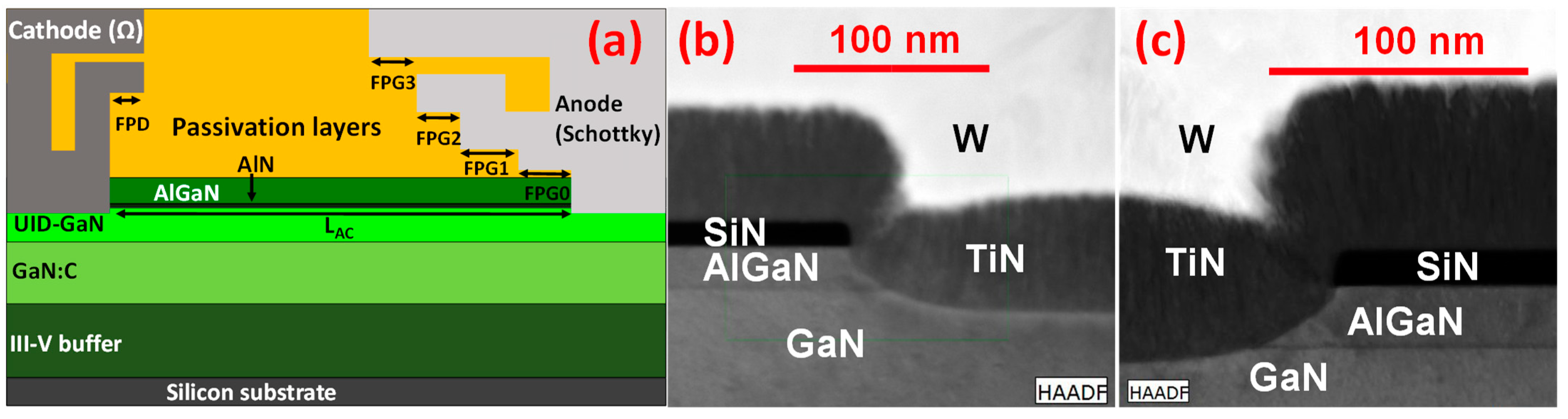
2. Materials and Methods
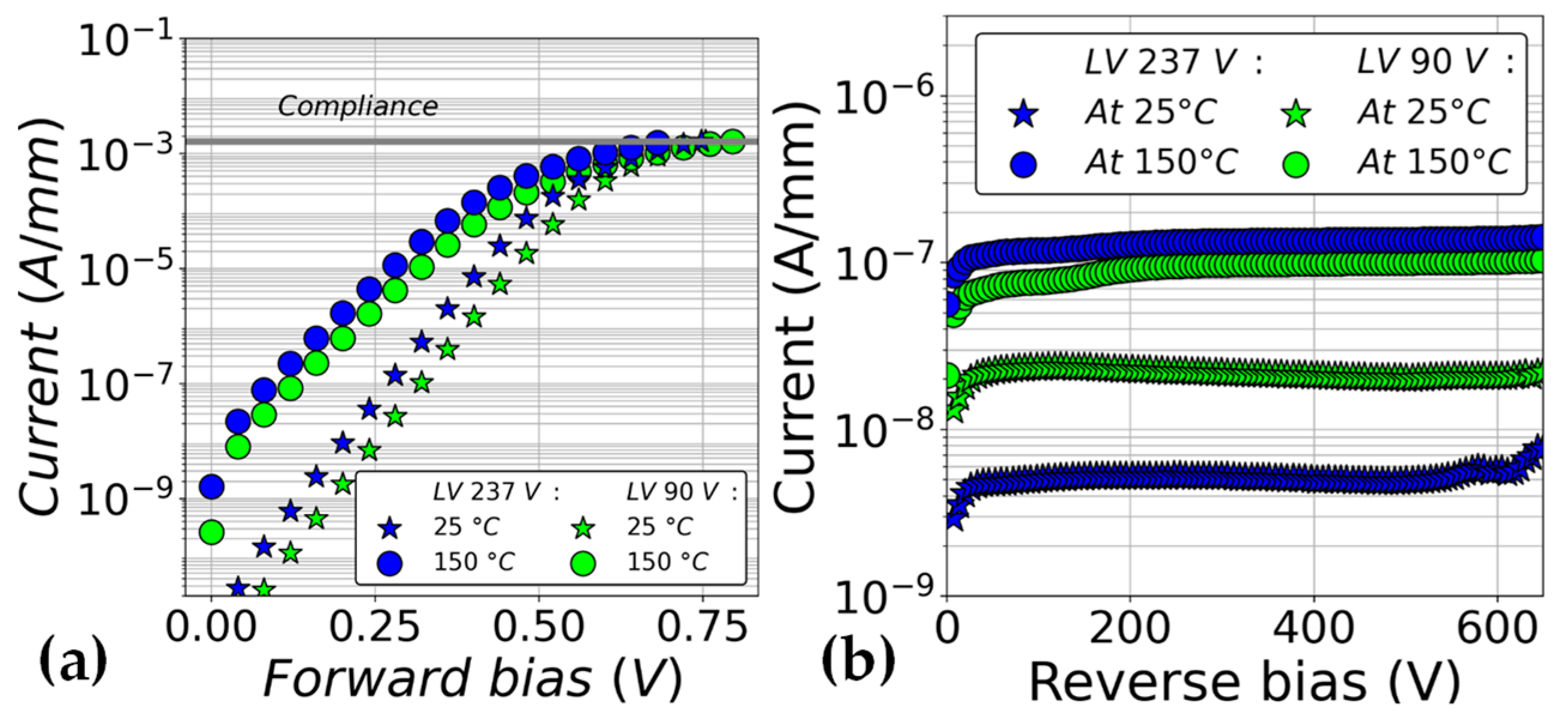
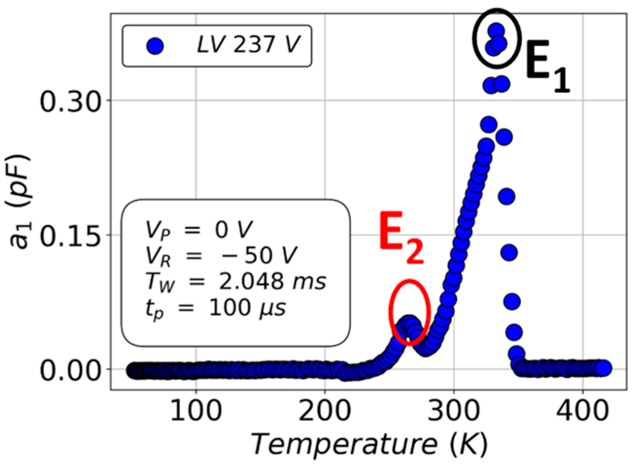
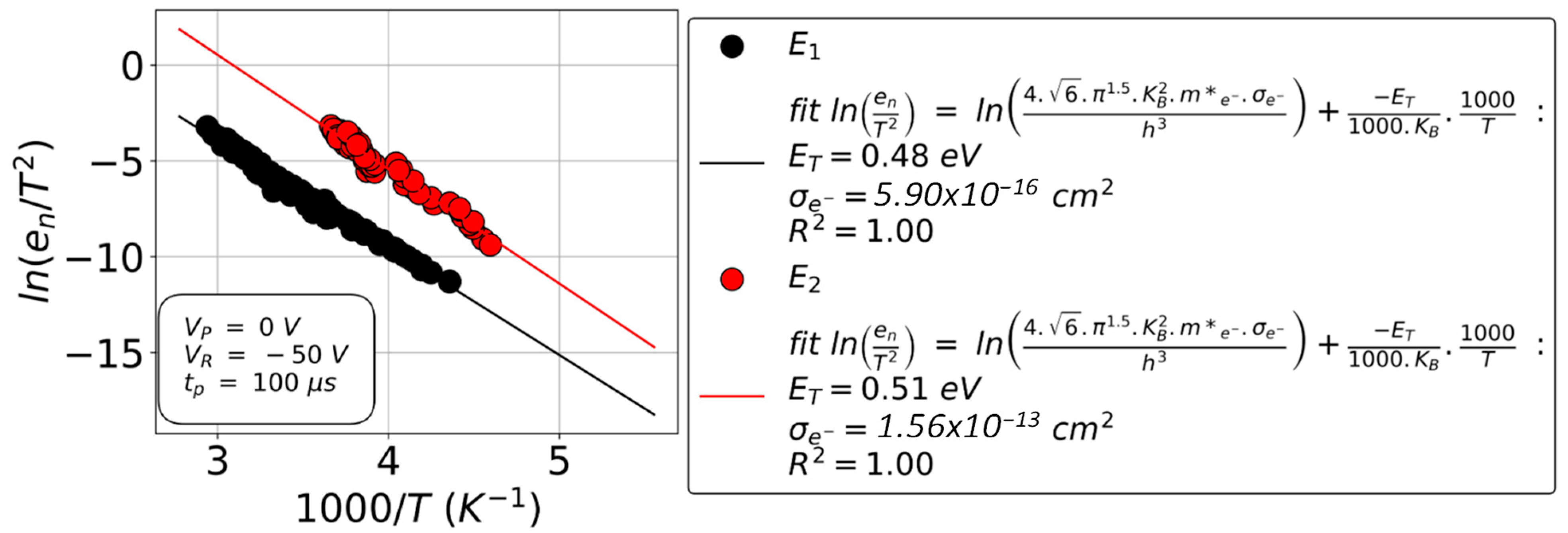
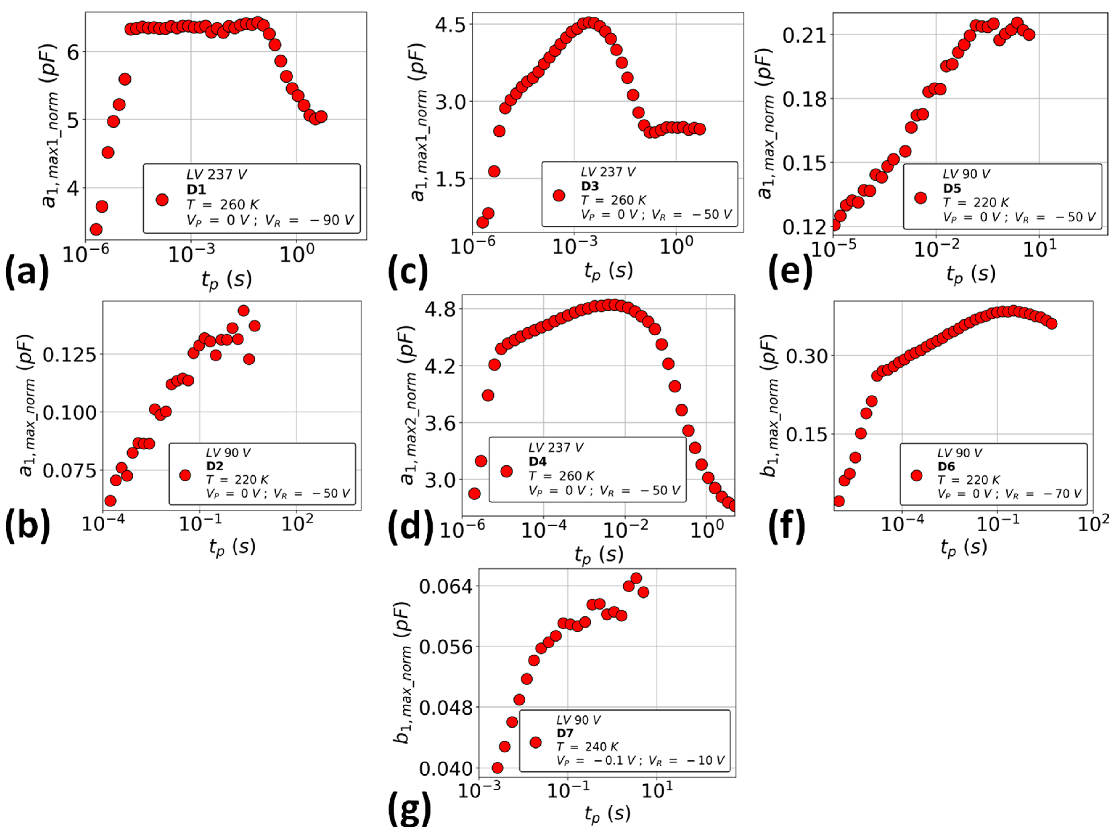
3. Results
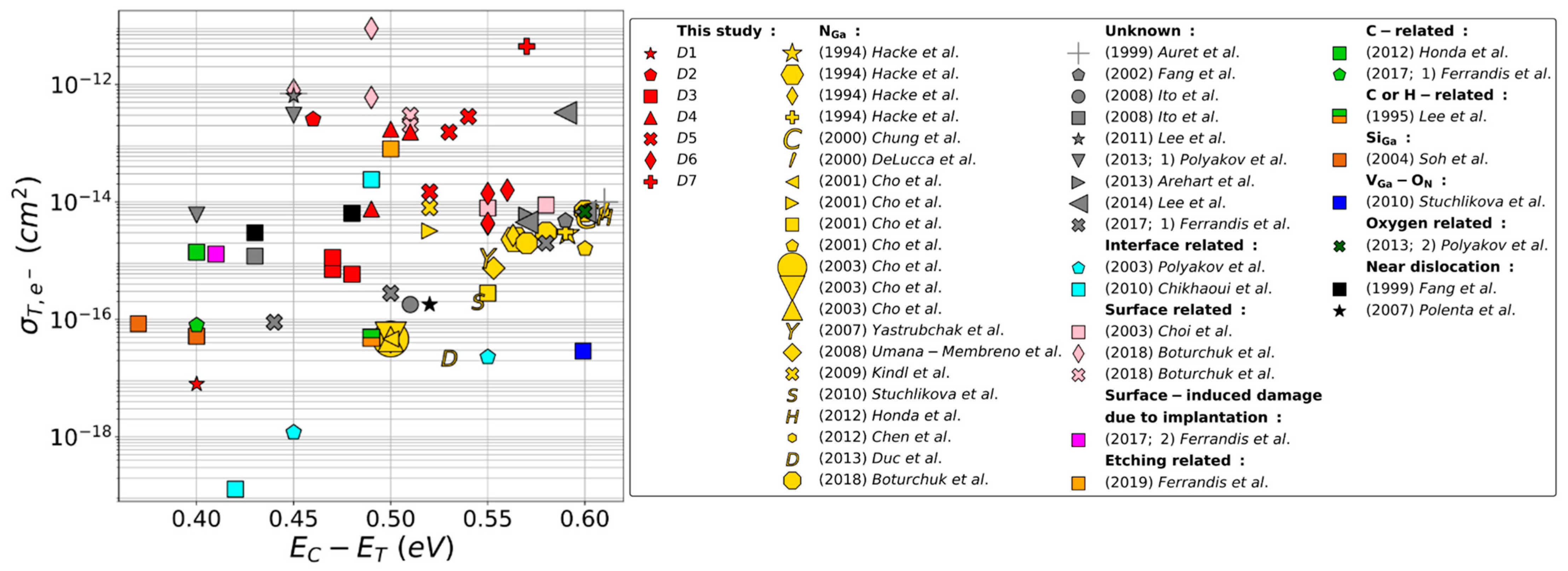
4. Discussion
5. Conclusions
Author Contributions
Funding
Data Availability Statement
Conflicts of Interest
References
- Meneghini, M.; De Santi, C.; Abid, I.; Buffolo, M.; Cioni, M.; Khadar, R.A.; Nela, L.; Zagni, N.; Chini, A.; Medjdoub, F.; et al. GaN-Based Power Devices: Physics, Reliability, and Perspectives. J. Appl. Phys. 2021, 130, 181101. [Google Scholar] [CrossRef]
- Di Paolo Emilio, M. Markets Turn to Wide-Bandgap Semiconductors to Increase Power Efficiency. EE Times Eur. 2020. Available online: https://www.eetimes.eu/markets-turn-to-wide-bandgap-semiconductors-to-increase-power-efficiency/2/ (accessed on 29 December 2022).
- Zhao, X.; Yeh, C.-S.; Chen, C.-W.; Lai, J.-S. A Comprehensive Comparison of MHz GaN-Based ZVS Step-Down Converters for Low Power Integrated On-Chip Applications. In Proceedings of the 2018 IEEE Energy Conversion Congress and Exposition (ECCE), Portland, OR, USA, 23–27 September 2018; pp. 5271–5275. [Google Scholar] [CrossRef]
- Mohammad, S.N.; Salvador, A.A.; Morkoc, H. Emerging Gallium Nitride Based Devices. Proc. IEEE 1995, 83, 1306–1355. [Google Scholar] [CrossRef]
- Gaskill, D.K.; Brandt, C.D.; Nemanich, R.J. (Eds.) III-Nitride, SiC, and Diamond Materials for Electronic Devices, San Francisco, CA, USA, 8–12 April 1996; Materials Research Society: Pittsburgh, PA, USA, 1996; ISBN 978-1-55899-326-6. [Google Scholar]
- Soni, A.; Shikha, S.; Shrivastava, M. On the Role of Interface States in AlGaN/GaN Schottky Recessed Diodes: Physical Insights, Performance Tradeoff, and Engineering Guidelines. IEEE Trans. Electron Devices 2019, 66, 2569–2576. [Google Scholar] [CrossRef]
- Uren, M.J.; Silvestri, M.; Casar, M.; Hurkx, G.A.M.; Croon, J.A.; Sonsky, J.; Kuball, M. Intentionally Carbon-Doped AlGaN/GaN HEMTs: Necessity for Vertical Leakage Paths. IEEE Electron Device Lett. 2014, 35, 327–329. [Google Scholar] [CrossRef] [Green Version]
- Wach, F.; Uren, M.J.; Bakeroot, B.; Zhao, M.; Decoutere, S.; Kuball, M. Low Field Vertical Charge Transport in the Channel and Buffer Layers of GaN-on-Si High Electron Mobility Transistors. IEEE Electron Device Lett. 2020, 41, 1754–1757. [Google Scholar] [CrossRef]
- Choi, K.J.; Jang, H.W.; Lee, J.-L. Observation of Inductively Coupled-Plasma-Induced Damage on n-Type GaN Using Deep-Level Transient Spectroscopy. Appl. Phys. Lett. 2003, 82, 1233–1235. [Google Scholar] [CrossRef] [Green Version]
- Fang, Z.-Q.; Look, D.C.; Wang, X.-L.; Han, J.; Khan, F.A.; Adesida, I. Plasma-Etching-Enhanced Deep Centers in n-GaN Grown by Metalorganic Chemical-Vapor Deposition. Appl. Phys. Lett. 2003, 82, 1562–1564. [Google Scholar] [CrossRef] [Green Version]
- Cho, H.K.; Khan, F.A.; Adesida, I.; Fang, Z.-Q.; Look, D.C. Deep Level Characteristics in N-GaN with Inductively Coupled Plasma Damage. J. Phys. D Appl. Phys. 2008, 41, 155314. [Google Scholar] [CrossRef]
- Ferrandis, P.; Charles, M.; Baines, Y.; Buckley, J.; Garnier, G.; Gillot, C.; Reimbold, G. Ion-Assisted Gate Recess Process Induced Damage in GaN Channel of AlGaN/GaN Schottky Barrier Diodes Studied by Deep Level Transient Spectroscopy. Jpn. J. Appl. Phys. 2017, 56, 04CG01. [Google Scholar] [CrossRef]
- Stuchlikova, L.; Sebok, J.; Rybar, J.; Petrus, M.; Nemec, M.; Harmatha, L.; Benkovska, J.; Kovac, J.; Skriniarova, J.; Lalinsky, T.; et al. Investigation of Deep Energy Levels in Heterostructures Based on GaN by DLTS. In Proceedings of the 8th International Conference on Advanced Semiconductor Devices & Microsystems (ASDAM), Smolenice Castle, Slovakia, 25–27 October 2010; pp. 135–138. [Google Scholar] [CrossRef]
- Chikhaoui, W.; Bluet, J.M.; Bru-Chevallier, C.; Dua, C.; Aubry, R. Deep Traps Analysis in AlGaN/GaN Heterostructure Transistors. Phys. Status Solidi (C) 2010, 7, 92–95. [Google Scholar] [CrossRef]
- Hwang, Y.-S.; Liu, L.; Ren, F.; Polyakov, A.Y.; Smirnov, N.B.; Govorkov, A.V.; Kozhukhova, E.A.; Kolin, N.G.; Boiko, V.M.; Vereyovkin, S.S.; et al. Effect of Electron Irradiation on AlGaN/GaN and InAlN/GaN Heterojunctions. J. Vac. Sci. Technol. B Nanotechnol. Microelectron. Mater. Process. Meas. Phenom. 2013, 31, 22206. [Google Scholar] [CrossRef]
- Arehart, A.R.; Sasikumar, A.; Rajan, S.; Via, G.D.; Poling, B.; Winningham, B.; Heller, E.R.; Brown, D.; Pei, Y.; Recht, F.; et al. Direct Observation of 0.57eV Trap-Related RF Output Power Reduction in AlGaN/GaN High Electron Mobility Transistors. Solid-State Electron. 2013, 80, 19–22. [Google Scholar] [CrossRef]
- Polyakov, A.Y.; Smirnov, N.B.; Govorkov, A.V.; Kozhukhova, E.A.; Pearton, S.J.; Ren, F.; Lui, L.; Johnson, J.W.; Kargin, N.I.; Ryzhuk, R.V. Deep Centers and Persistent Photocapacitance in AlGaN/GaN High Electron Mobility Transistor Structures Grown on Si Substrates. J. Vac. Sci. Technol. B Nanotechnol. Microelectron. Mater. Process. Meas. Phenom. 2013, 31, 11211. [Google Scholar] [CrossRef]
- Polyakov, A.Y.; Smirnov, N.B.; Ha, M.-W.; Hahn, C.-K.; Kozhukhova, E.A.; Govorkov, A.V.; Ryzhuk, R.V.; Kargin, N.I.; Cho, H.-S.; Lee, I.-H. Effects of Annealing in Oxygen on Electrical Properties of AlGaN/GaN Heterostructures Grown on Si. J. Alloy. Compd. 2013, 575, 17–23. [Google Scholar] [CrossRef]
- Ferrandis, P.; Charles, M.; Gillot, C.; Escoffier, R.; Morvan, E.; Torres, A.; Reimbold, G. Effects of Negative Bias Stress on Trapping Properties of AlGaN/GaN Schottky Barrier Diodes. Microelectron. Eng. 2017, 178, 158–163. [Google Scholar] [CrossRef]
- Ferrandis, P.; El-Khatib, M.; Jaud, M.-A.; Morvan, E.; Charles, M.; Guillot, G.; Bremond, G. Study of Deep Traps in AlGaN/GaN High-Electron Mobility Transistors by Electrical Characterization and Simulation. J. Appl. Phys. 2019, 125, 35702. [Google Scholar] [CrossRef]
- Ferrandis, P.; Charles, M.; Veillerot, M.; Gillot, C. Analysis of Hole-like Traps in Deep Level Transient Spectroscopy Spectra of AlGaN/GaN Heterojunctions. J. Phys. D Appl. Phys. 2020, 53, 185105. [Google Scholar] [CrossRef]
- Lorin, T.; Vandendaele, W.; Gwoziecki, R.; Baines, Y.; Biscarrat, J.; Jaud, M.-A.; Gillot, C.; Charles, M.; Plissonnier, M.; Ghibaudo, G.; et al. On the Understanding of Cathode Related Trapping Effects in GaN-on-Si Schottky Diodes. IEEE J. Electron Devices Soc. 2018, 6, 956–964. [Google Scholar] [CrossRef]
- Sze, S.M.; Ng, K.K. Physics of Semiconductor Devices, 3rd ed.; Wiley-Interscience: Hoboken, NJ, USA, 2007; ISBN 978-0-471-14323-9. [Google Scholar]
- FT-1030 DLTFS; PhysTech GmbH: Moosburg, Germany, 2014.
- Zhang, T. Deep Levels Characterizations in SiC to Optimize High Voltage Devices. Ph.D. Thesis, Université de Lyon, Lyon, France, 2018. [Google Scholar]
- Weiss, S.; Kassing, R. Deep Level Transient Fourier Spectroscopy (DLTFS)—A Technique for the Analysis of Deep Level Properties. Solid-State Electron. 1988, 31, 1733–1742. [Google Scholar] [CrossRef]
- Kindl, D.; Hubík, P.; Krištofik, J.; Mareš, J.J.; Výborný, Z.; Leys, M.R.; Boeykens, S. Deep Defects in GaN/AlGaN/SiC Heterostructures. J. Appl. Phys. 2009, 105, 93706. [Google Scholar] [CrossRef]
- Vurgaftman, I.; Meyer, J.R.; Ram-Mohan, L.R. Band Parameters for III–V Compound Semiconductors and Their Alloys. J. Appl. Phys. 2001, 89, 5815–5875. [Google Scholar] [CrossRef] [Green Version]
- Provencher Algorithm; Automatic Software Packages. 2016. Available online: http://www.s-provencher.com/ (accessed on 29 December 2022).
- Provencher, S.W. CONTIN: A General Purpose Constrained Regularization Program for Inverting Noisy Linear Algebraic and Integral Equations. Comput. Phys. Commun. 1982, 27, 229–242. [Google Scholar] [CrossRef]
- Wosiński, T. Evidence for the Electron Traps at Dislocations in GaAs Crystals. J. Appl. Phys. 1989, 65, 6. [Google Scholar] [CrossRef]
- Yastrubchak, O.; Wosiński, T.; Mąkosa, A.; Figielski, T.; Porowski, S.; Grzegory, I.; Czernecki, R.; Perlin, P. Capture Kinetics at Deep-Level Electron Traps in GaN-Based Laser Diode. Phys. Status Solidi C 2007, 4, 2878–2882. [Google Scholar] [CrossRef]
- Soh, C.B.; Chua, S.J.; Lim, H.F.; Chi, D.Z.; Liu, W.; Tripathy, S. Identification of Deep Levels in GaN Associated with Dislocations. J. Phys. Condens. Matter 2004, 16, 6305–6315. [Google Scholar] [CrossRef]
- Polenta, L.; Castaldini, A.; Cavallini, A. Defect Characterization in GaN: Possible Influence of Dislocations in the Yellow-Band Features. J. Appl. Phys. 2007, 102, 63702. [Google Scholar] [CrossRef]
- Cho, H.K.; Kim, C.S.; Hong, C.-H. Electron Capture Behaviors of Deep Level Traps in Unintentionally Doped and Intentionally Doped n -Type GaN. J. Appl. Phys. 2003, 94, 1485–1489. [Google Scholar] [CrossRef]
- Cho, H.K.; Kim, K.S.; Hong, C.-H.; Lee, H.J. Electron Traps and Growth Rate of Buffer Layers in Unintentionally Doped GaN. J. Cryst. Growth 2001, 223, 38–42. [Google Scholar] [CrossRef]
- Hacke, P.; Detchprohm, T.; Hiramatsu, K.; Sawaki, N.; Tadatomo, K.; Miyake, K. Analysis of Deep Levels in N-type GaN by Transient Capacitance Methods. J. Appl. Phys. 1994, 76, 304–309. [Google Scholar] [CrossRef]
- Umana-Membreno, G.A.; Parish, G.; Fichtenbaum, N.; Keller, S.; Mishra, U.K.; Nener, B.D. Electrically Active Defects in GaN Layers Grown With and Without Fe-Doped Buffers by Metal-Organic Chemical Vapor Deposition. J. Electron. Mater. 2008, 37, 569–572. [Google Scholar] [CrossRef]
- Duc, T.T.; Pozina, G.; Janzén, E.; Hemmingsson, C. Investigation of Deep Levels in Bulk GaN Material Grown by Halide Vapor Phase Epitaxy. J. Appl. Phys. 2013, 114, 153702. [Google Scholar] [CrossRef] [Green Version]
- Boturchuk, I.; Scheffler, L.; Larsen, A.N.; Julsgaard, B. Evolution of Electrically Active Defects in N-GaN During Heat Treatment Typical for Ohmic Contact Formation. Phys. Status Solidi A 2018, 215, 1700516. [Google Scholar] [CrossRef]
- Chung, H.M.; Chuang, W.C.; Pan, Y.C.; Tsai, C.C.; Lee, M.C.; Chen, W.H.; Chen, W.K.; Chiang, C.I.; Lin, C.H.; Chang, H. Electrical Characterization of Isoelectronic In-Doping Effects in GaN Films Grown by Metalorganic Vapor Phase Epitaxy. Appl. Phys. Lett. 2000, 76, 897–899. [Google Scholar] [CrossRef]
- Honda, U.; Yamada, Y.; Tokuda, Y.; Shiojima, K. Deep Levels in N-GaN Doped with Carbon Studied by Deep Level and Minority Carrier Transient Spectroscopies. Jpn. J. Appl. Phys. 2012, 51, 04DF04. [Google Scholar] [CrossRef]
- Chen, S.; Honda, U.; Shibata, T.; Matsumura, T.; Tokuda, Y.; Ishikawa, K.; Hori, M.; Ueda, H.; Uesugi, T.; Kachi, T. As-Grown Deep-Level Defects in n-GaN Grown by Metal–Organic Chemical Vapor Deposition on Freestanding GaN. J. Appl. Phys. 2012, 112, 53513. [Google Scholar] [CrossRef]
- DeLucca, J.M.; Mohney, S.E.; Auret, F.D.; Goodman, S.A. Pt Schottky Contacts to N-GaN Formed by Electrodeposition and Physical Vapor Deposition. J. Appl. Phys. 2000, 88, 2593–2600. [Google Scholar] [CrossRef]
- Auret, F.D.; Goodman, S.A.; Koschnick, F.K.; Spaeth, J.-M.; Beaumont, B.; Gibart, P. Proton Bombardment-Induced Electron Traps in Epitaxially Grown n-GaN. Appl. Phys. Lett. 1999, 74, 407–409. [Google Scholar] [CrossRef]
- Lee, I.-H.; Polyakov, A.Y.; Smirnov, N.B.; Govorkov, A.V.; Kozhukhova, E.A.; Kolin, N.G.; Boiko, V.M.; Korulin, A.V.; Pearton, S.J. Deep Electron and Hole Traps in Neutron Transmutation Doped N-GaN. J. Vac. Sci. Technol. B Nanotechnol. Microelectron. Mater. Process. Meas. Phenom. 2011, 29, 41201. [Google Scholar] [CrossRef]
- Ito, T.; Nomura, Y.; Selvaraj, S.L.; Egawa, T. Comparison of Electrical Properties in GaN Grown on Si(111) and c-Sapphire Substrate by MOVPE. J. Cryst. Growth 2008, 310, 4896–4899. [Google Scholar] [CrossRef]
- Fang, Z.-Q.; Look, D.C.; Polenta, L. Dislocation-Related Electron Capture Behaviour of Traps in n-Type GaN. J. Phys. Condens. Matter 2002, 14, 13061–13068. [Google Scholar] [CrossRef]
- Lee, I.-H.; Polyakov, A.Y.; Smirnov, N.B.; Hahn, C.-K.; Pearton, S.J. Spatial Location of the Ec-0.6 EV Electron Trap in AlGaN/GaN Heterojunctions. J. Vac. Sci. Technol. B Nanotechnol. Microelectron. Mater. Process. Meas. Phenom. 2014, 32, 50602. [Google Scholar] [CrossRef]
- Polyakov, A.Y.; Smirnov, N.B.; Govorkov, A.V.; Mil, M.G.; Pearton, S.J.; Usikov, A.S.; Shmidt, N.M.; Osinsky, A.V.; Lundin, W.V.; Zavarin, E.E.; et al. Deep Levels Studies of AlGaN/GaN Superlattices. Solid-State Electron. 2003, 47, 671–676. [Google Scholar] [CrossRef]
- Lee, W.I.; Huang, T.C.; Guo, J.D.; Feng, M.S. Effects of Column III Alkyl Sources on Deep Levels in GaN Grown by Organometallic Vapor Phase Epitaxy. Appl. Phys. Lett. 1995, 67, 1721–1723. [Google Scholar] [CrossRef]
- Fang, Z.-Q.; Look, D.C.; Kim, W.; Morkoç, H. Characteristics of Deep Centers Observed in N-GaN Grown by Reactive Molecular Beam Epitaxy. MRS Online Proc. Libr. (OPL) 1999, 595, 6. [Google Scholar] [CrossRef]
- Jenkins, D.W.; Dow, J.D. Electronic Structures and Doping of InN, InxGa1−xN, and InxAl1−xN. Phys. Rev. B 1989, 39, 3317–3329. [Google Scholar] [CrossRef] [PubMed]
- Gorczyca, I.; Svane, A.; Christensen, N.E. Theory of Point Defects in GaN, AlN, and BN: Relaxation and Pressure Effects. Phys. Rev. B 1999, 60, 8147–8157. [Google Scholar] [CrossRef] [Green Version]
- Matsubara, M.; Bellotti, E. A First-Principles Study of Carbon-Related Energy Levels in GaN. I. Complexes Formed by Substitutional/Interstitial Carbons and Gallium/Nitrogen Vacancies. J. Appl. Phys. 2017, 121, 195701. [Google Scholar] [CrossRef] [Green Version]
- Zhong, J.; Yao, Y.; Zheng, Y.; Yang, F.; Ni, Y.-Q.; He, Z.-Y.; Shen, Z.; Zhou, G.-L.; Zhou, D.-Q.; Wu, Z.-S.; et al. Influence of Dry-Etching Damage on the Electrical Properties of an AlGaN/GaN Schottky Barrier Diode with Recessed Anode. Chin. Phys. B 2015, 24, 97303. [Google Scholar] [CrossRef]
- Tanaka, T.; Shiojima, K.; Mishima, T.; Tokuda, Y. Deep-Level Transient Spectroscopy of Low-Free-Carrier-Concentration n-GaN Layers Grown on Freestanding GaN Substrates: Dependence on Carbon Compensation Ratio. Jpn. J. Appl. Phys. 2016, 55, 61101. [Google Scholar] [CrossRef]
- Arehart, A.R.; Corrion, A.; Poblenz, C.; Speck, J.S.; Mishra, U.K.; Ringel, S.A. Deep Level Optical and Thermal Spectroscopy of Traps in N-GaN Grown by Ammonia Molecular Beam Epitaxy. Appl. Phys. Lett. 2008, 93, 112101. [Google Scholar] [CrossRef]
- Polyakov, A.Y.; Smirnov, N.B.; Kozhukhova, E.A. Temperature Stability of High-Resistivity GaN Buffer Layers Grown by Metalorganic Chemical Vapor Deposition. J. Vac. Sci. Technol. B 2013, 31, 8. [Google Scholar] [CrossRef]
- Götz, W.; Johnson, N.M.; Amano, H.; Akasaki, I. Deep Level Defects in N-type GaN. Appl. Phys. Lett. 1994, 65, 463–465. [Google Scholar] [CrossRef]
- Haase, D.; Schmid, M.; Kürner, W.; Dörnen, A.; Härle, V.; Scholz, F.; Burkard, M.; Schweizer, H. Deep-level Defects and N-type-carrier Concentration in Nitrogen Implanted GaN. Appl. Phys. Lett. 1996, 69, 2525–2527. [Google Scholar] [CrossRef]

| Experimental Split | ICP Source (W) | RF Bias (V) | BCl3/Cl2 Ratio |
|---|---|---|---|
| LV 90 V | 500 | 90 | 1 |
| LV 237 V | 300 | 237 | 4 |
| D1 | D2 | D3 | D4 | D5 | D6 | D7 | |||||||||
|---|---|---|---|---|---|---|---|---|---|---|---|---|---|---|---|
| ET (eV) | σ (cm2) | ET (eV) | σ (cm2) | ET (eV) | σ (cm2) | ET (eV) | σ (cm2) | ET (eV) | σ (cm2) | ET (eV) | σ (cm2) | ET (eV) | σ (cm2) | ||
| UP = −0.1 V UR = −10 V | LV 237 V | 0.53 | 1.55 × 10⁻¹³ | ||||||||||||
| LV 90 V | 0.57 | 4.45 × 10⁻¹² | |||||||||||||
| UP = −0.1 V UR = −20 V | LV 237 V | 0.50 | 1.73 × 10⁻¹³ | ||||||||||||
| LV 90 V | 0.49 | 7.58 × 10⁻¹⁵ | 0.54 | 2.85 × 10⁻¹³ | |||||||||||
| UP = 0 V UR = −50 V | LV 237 V | 0.48 | 5.90 × 10⁻¹⁶ | 0.51 | 1.56 × 10⁻¹³ | ||||||||||
| LV 90 V | 0.46 | 2.56 × 10⁻¹³ | 0.52 | 1.49 × 10⁻¹⁴ | |||||||||||
| UP = 0 V UR = −70 V | LV 237 V | 0.47 | 7.14 × 10⁻¹⁶ | 0.55 | 4.33 × 10⁻¹⁵ | ||||||||||
| LV 90 V | 0.55 | 1.39 × 10⁻¹⁴ | |||||||||||||
| UP = 0 V UR = −90 V | LV 237 V | 0.40 | 7.98 × 10⁻¹⁸ | 0.47 | 1.13 × 10⁻¹⁵ | 0.55 | 4.21 × 10⁻¹⁵ | ||||||||
| LV 90 V | 0.56 | 1.59 × 10⁻¹⁴ | |||||||||||||
| Proposed Hypothesis | CGa-VN | Surface recombination | Etching-related | Native defects or related complex | CN-CGa | NGa | Etching-related | ||||||||
Disclaimer/Publisher’s Note: The statements, opinions and data contained in all publications are solely those of the individual author(s) and contributor(s) and not of MDPI and/or the editor(s). MDPI and/or the editor(s) disclaim responsibility for any injury to people or property resulting from any ideas, methods, instructions or products referred to in the content. |
© 2023 by the authors. Licensee MDPI, Basel, Switzerland. This article is an open access article distributed under the terms and conditions of the Creative Commons Attribution (CC BY) license (https://creativecommons.org/licenses/by/4.0/).
Share and Cite
Rigaud-Minet, F.; Raynaud, C.; Buckley, J.; Charles, M.; Pimenta-Barros, P.; Gwoziecki, R.; Gillot, C.; Sousa, V.; Morel, H.; Planson, D. Deep Level Transient Fourier Spectroscopy Investigation of Electron Traps on AlGaN/GaN-on-Si Power Diodes. Energies 2023, 16, 599. https://doi.org/10.3390/en16020599
Rigaud-Minet F, Raynaud C, Buckley J, Charles M, Pimenta-Barros P, Gwoziecki R, Gillot C, Sousa V, Morel H, Planson D. Deep Level Transient Fourier Spectroscopy Investigation of Electron Traps on AlGaN/GaN-on-Si Power Diodes. Energies. 2023; 16(2):599. https://doi.org/10.3390/en16020599
Chicago/Turabian StyleRigaud-Minet, Florian, Christophe Raynaud, Julien Buckley, Matthew Charles, Patricia Pimenta-Barros, Romain Gwoziecki, Charlotte Gillot, Véronique Sousa, Hervé Morel, and Dominique Planson. 2023. "Deep Level Transient Fourier Spectroscopy Investigation of Electron Traps on AlGaN/GaN-on-Si Power Diodes" Energies 16, no. 2: 599. https://doi.org/10.3390/en16020599