

A Novel Analytical Formulation of SiC-MOSFET Losses to Size High-Efficiency Three-Phase Inverters


Abstract
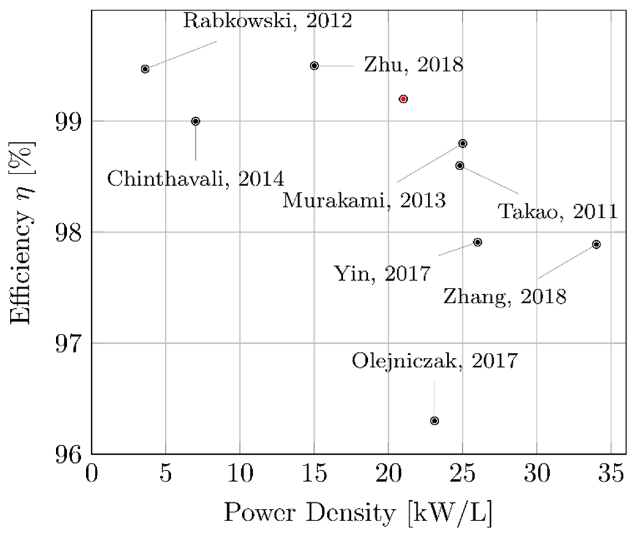
:1. Introduction
2. Three-Phase Inverter Efficiency Formulation
2.1. Computation of the Conduction Losses Ratio Pon/Psw
2.2. Computation of the Switching Losses
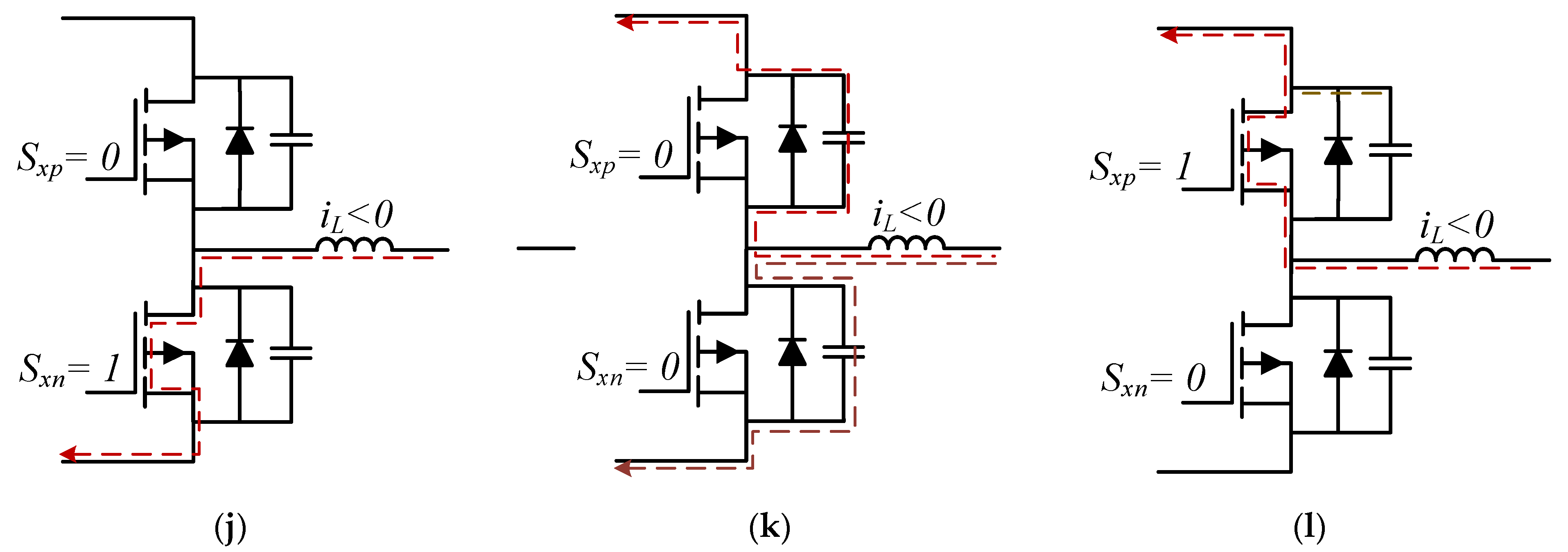
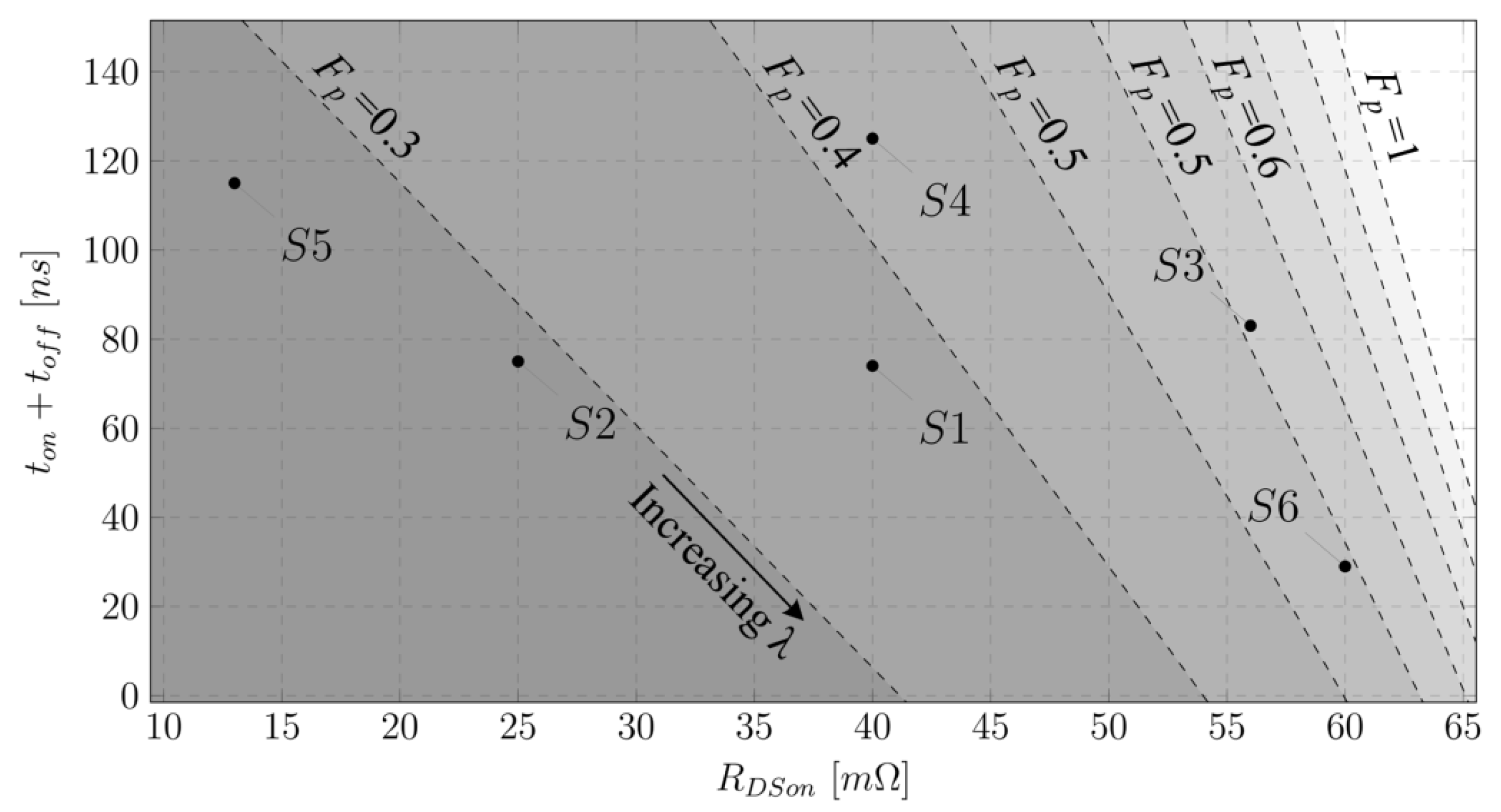
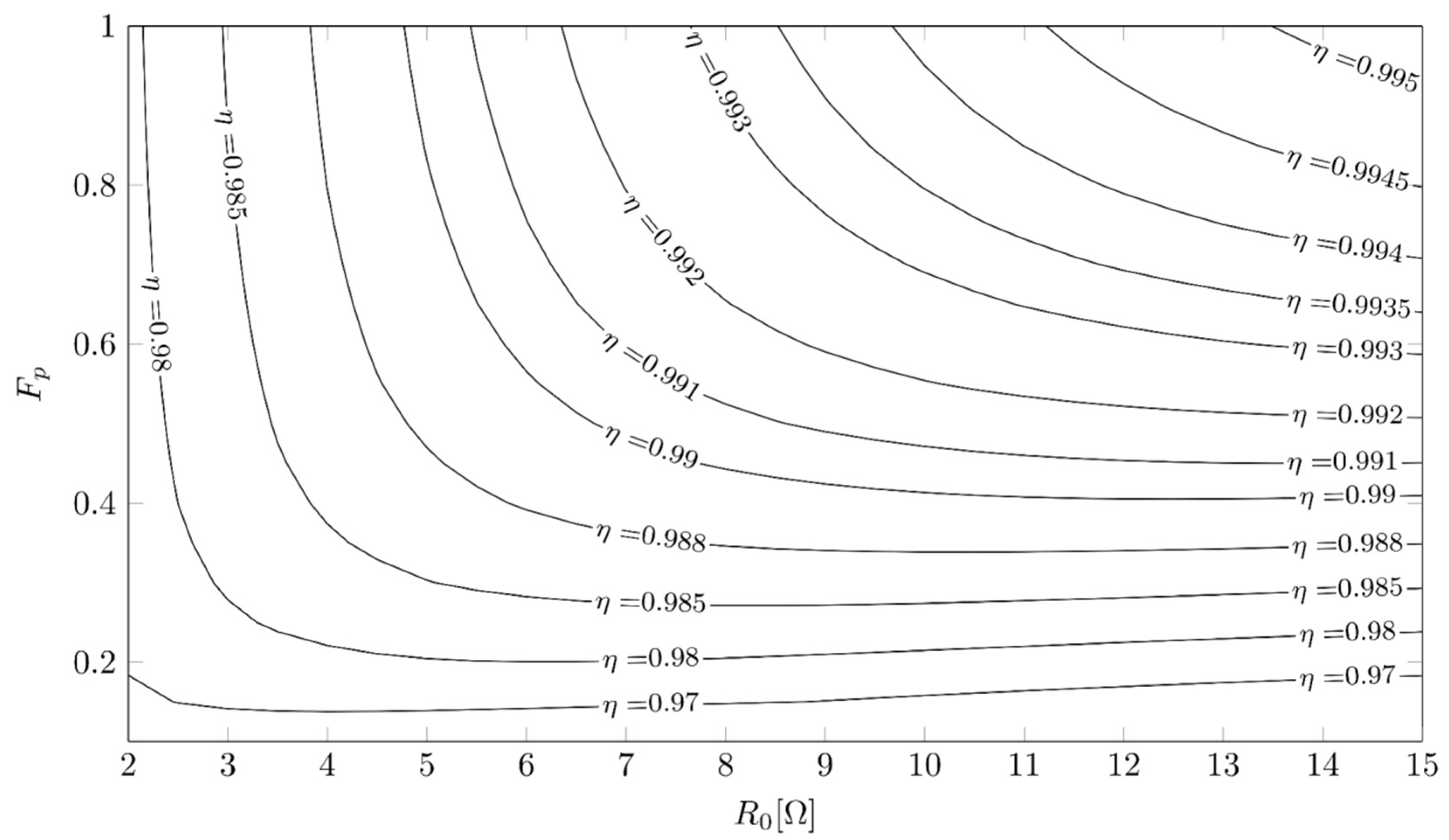
3. Considerations of the Proposed Methodology, Semiconductor Selection, and Case Study
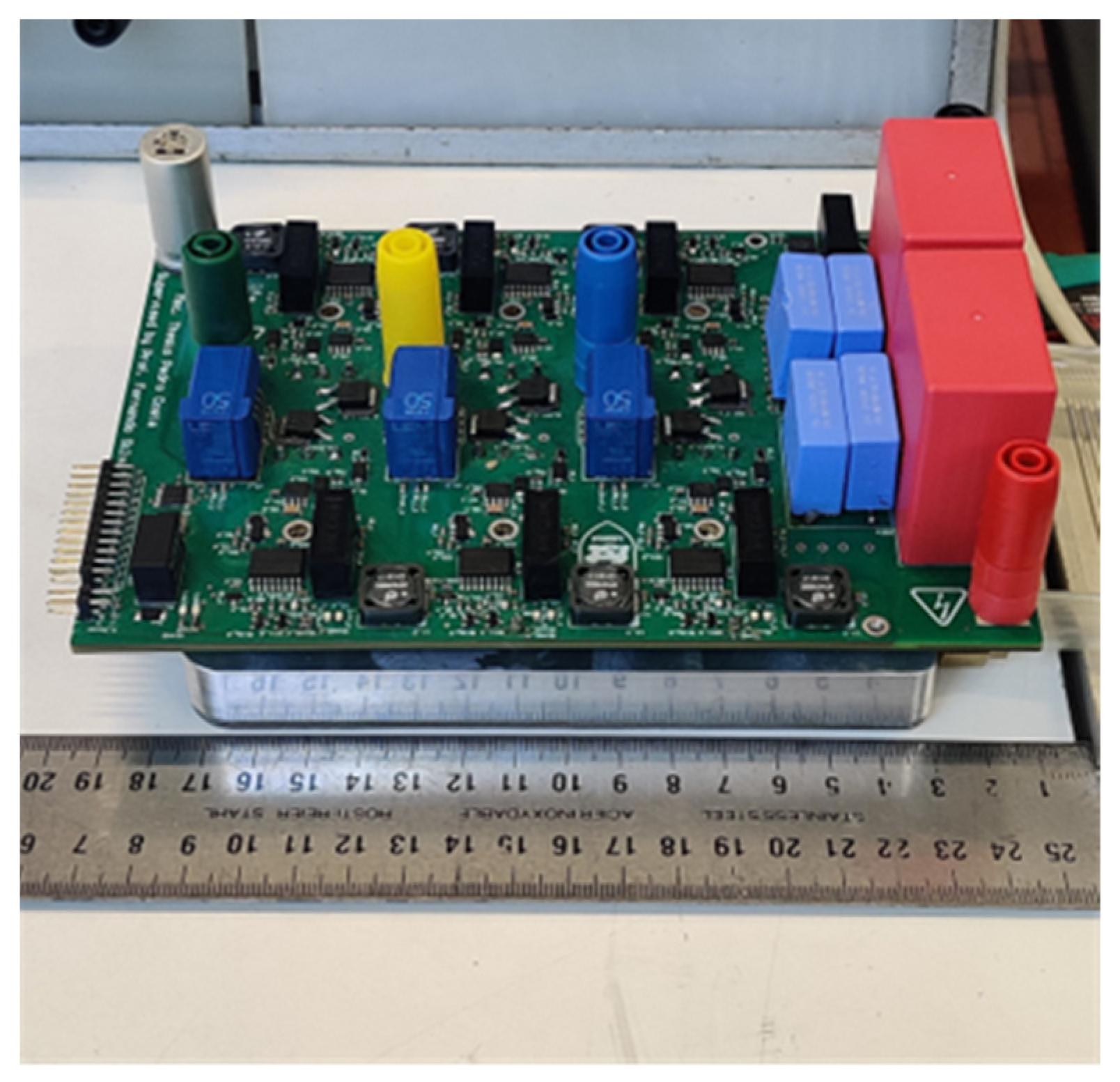
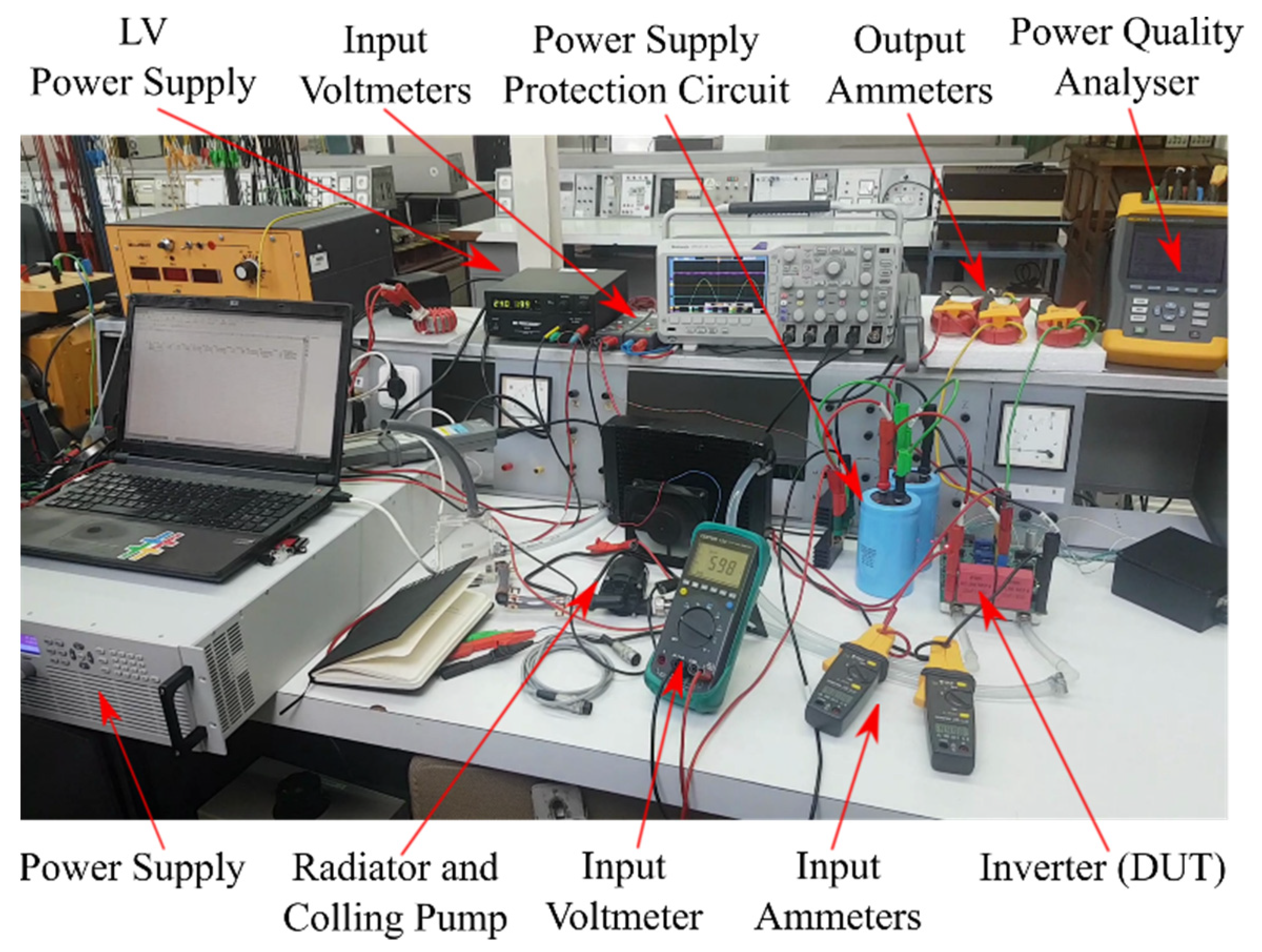
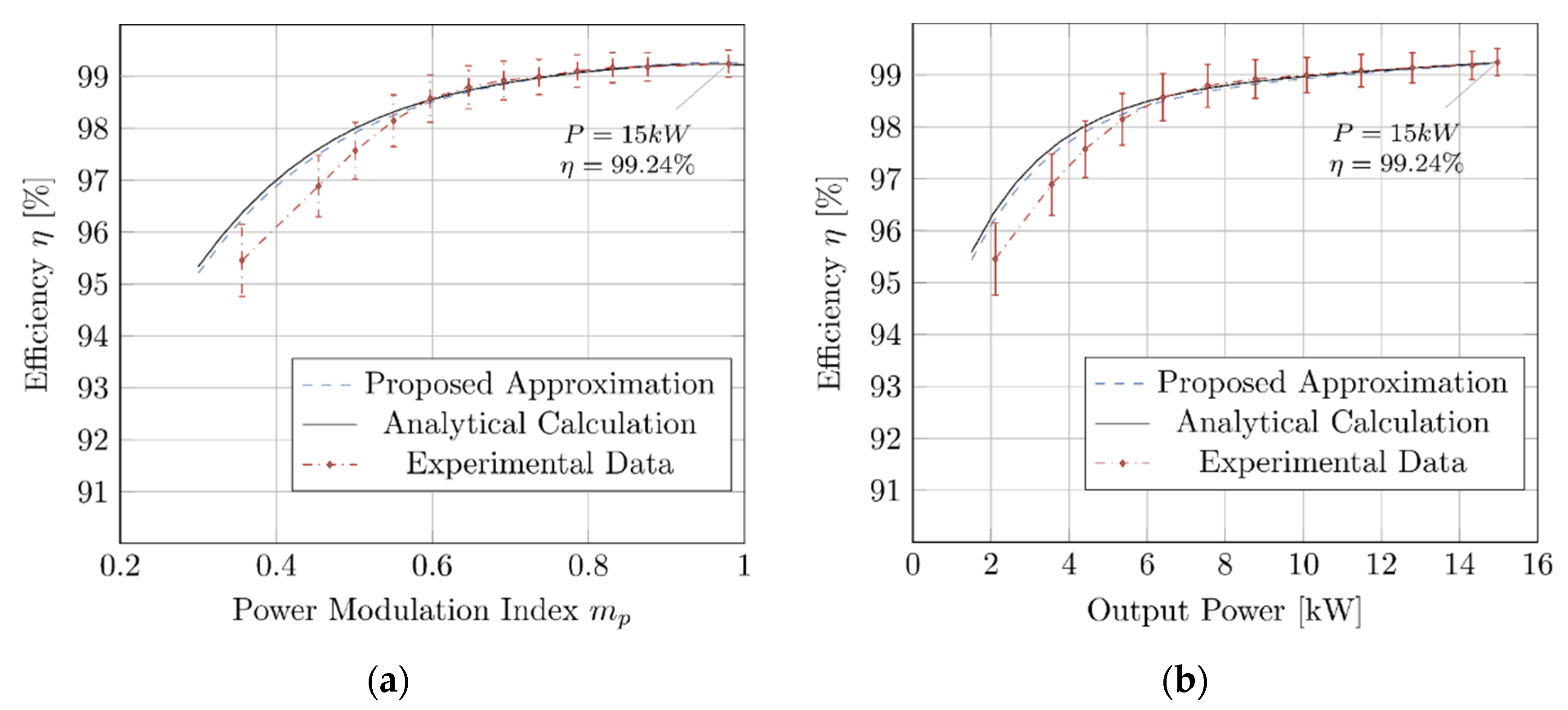
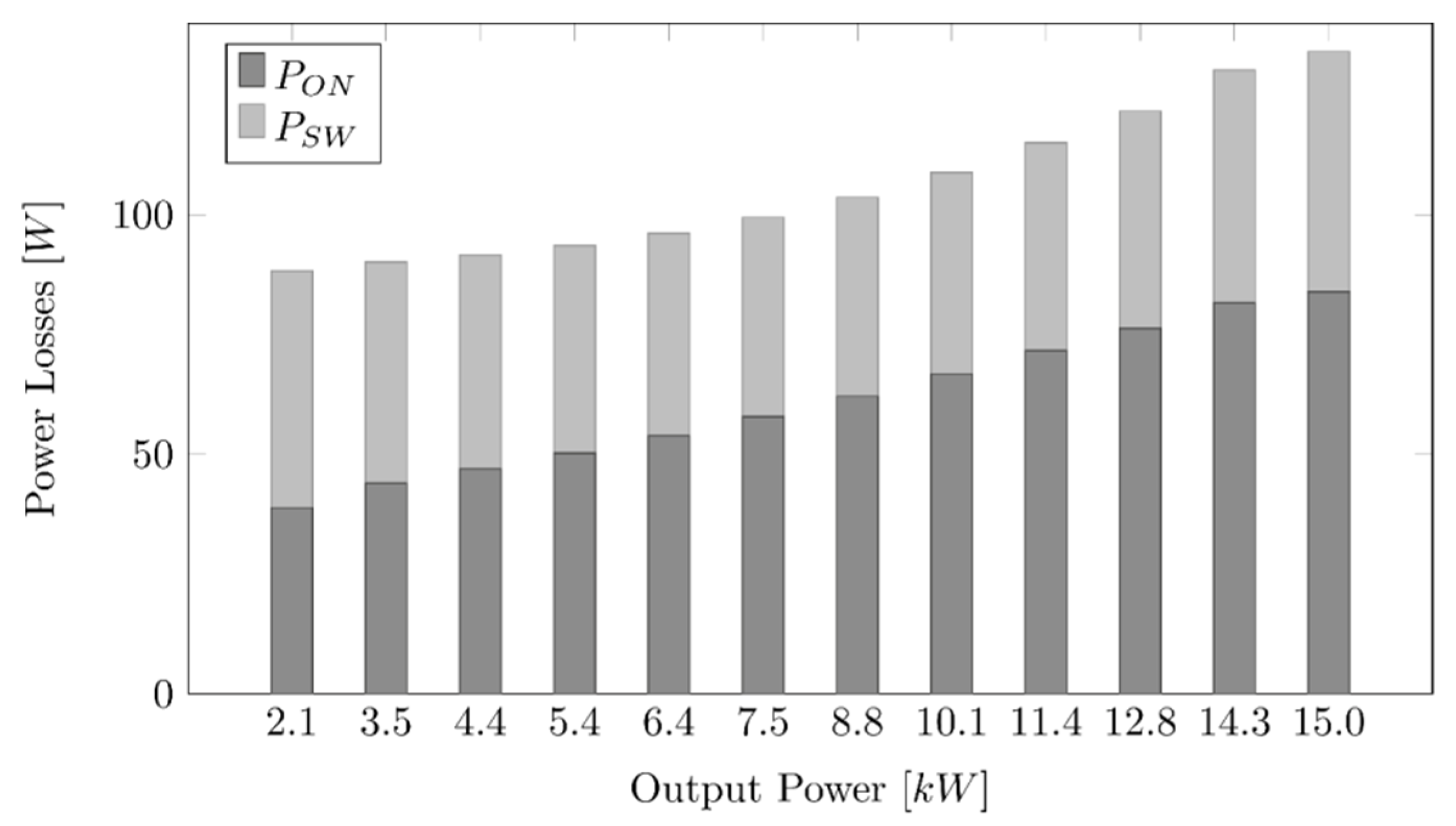
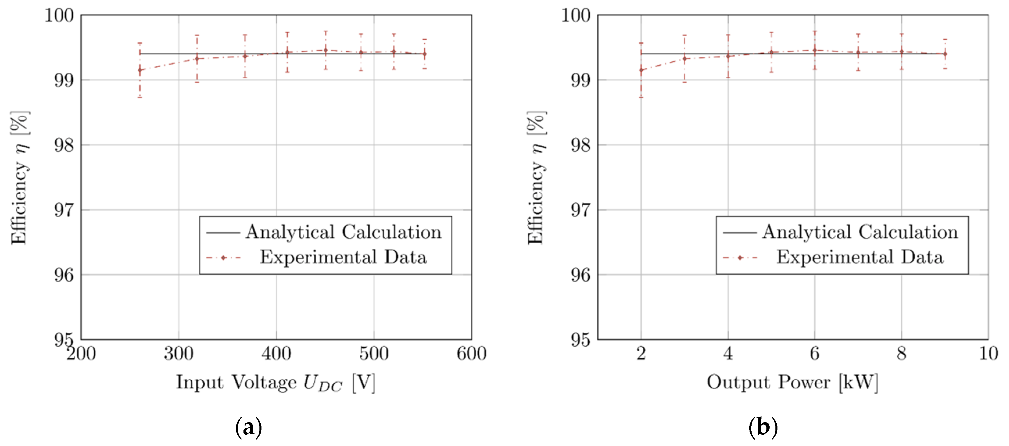
4. Experimental Results
5. Conclusions
Author Contributions
Funding
Data Availability Statement
Conflicts of Interest
Appendix A
Appendix B
References
- Furuhashi, M.; Tomohisa, S.; Kuroiwa, T.; Yamakawa, S. Practical Applications of SiC-MOSFETs and Further Developments. Semicond. Sci. Technol. 2016, 31, 034003. [Google Scholar] [CrossRef]
- Rabkowski, J.; Peftitsis, D.; Nee, H.P. Silicon Carbide Power Transistors: A New Era in Power Electronics Is Initiated. IEEE Ind. Electron. Mag. 2012, 6, 17–26. [Google Scholar] [CrossRef]
- Biela, J.; Schweizer, M.; Waffler, S.; Kolar, J.W. SiC versus Si—Evaluation of Potentials for Performance Improvement of Inverter and DCDC Converter Systems by SiC Power Semiconductors. IEEE Trans. Ind. Electron. 2011, 58, 2872–2882. [Google Scholar] [CrossRef]
- Han, D.; Noppakunkajorn, J.; Sarlioglu, B. Comprehensive Efficiency, Weight, and Volume Comparison of SiC- and Si-Based Bidirectional Dc-Dc Converters for Hybrid Electric Vehicles. IEEE Trans. Veh. Technol. 2014, 63, 3001–3010. [Google Scholar] [CrossRef]
- She, X.; Huang, A.Q.; Ozpineci, B. Review of Silicon Carbide Power Devices and Their Applications. IEEE Trans. Ind. Electron. 2017, 64, 8193–8205. [Google Scholar] [CrossRef]
- Zhang, H.; Tolbert, L.M.; Ozpineci, B. Impact of SiC Devices on Hybrid Electric and Plug-in Hybrid Electric Vehicles. IEEE Trans. Ind. Appl. 2011, 47, 912–921. [Google Scholar] [CrossRef]
- Ding, X.; Cheng, J.; Chen, F. Impact of Silicon Carbide Devices on the Powertrain Systems in Electric Vehicles. Energies 2017, 10, 533. [Google Scholar] [CrossRef] [Green Version]
- Yin, S.; Tseng, K.J.; Tong, C.F.; Simanjorang, R.; Gajanayake, C.J.; Gupta, A.K. A 99% Efficiency SiC Three-Phase Inverter Using Synchronous Rectification. In Proceedings of the 2016 IEEE Applied Power Electronics Conference and Exposition (APEC), Long Beach, CA, USA, 20–24 March 2016; pp. 2942–2949. [Google Scholar] [CrossRef]
- Rabkowski, J.; Peftitsis, D.; Nee, H.P. Design Steps towards a 40-KVA SiC Inverter with an Efficiency Exceeding 99.5%. In Proceedings of the 2012 Twenty-Seventh Annual IEEE Applied Power Electronics Conference and Exposition (APEC), Orlando, FL, USA, 5–9 February 2012; pp. 1536–1543. [Google Scholar] [CrossRef]
- Zhu, J.; Kim, H.; Chen, H.; Erickson, R.; Maksimovic, D. High Efficiency SiC Traction Inverter for Electric Vehicle Applications. In Proceedings of the 2018 IEEE Applied Power Electronics Conference and Exposition (APEC), San Antonio, TX, USA, 4–8 March 2018; pp. 1428–1433. [Google Scholar] [CrossRef]
- Colmenares, J.; Peftitsis, D.; Sadik, D.; Nee, H. High-Efficiency Three-Phase Inverter with SiC MOSFET Power Modules for Motor-Drive Applications. In Proceedings of the 2014 IEEE Energy Conversion Congress and Exposition (ECCE), Pittsburgh, PA, USA, 14–18 September 2014; pp. 468–474. [Google Scholar]
- Chinthavali, M.; Ayers, C.; Campbell, S.; Wiles, R.; Ozpineci, B. A 10-KW SiC Inverter with a Novel Printed Metal Power Module with Integrated Cooling Using Additive Manufacturing. In Proceedings of the 2014 IEEE Workshop on Wide Bandgap Power Devices and Applications, Knoxville, TN, USA, 13–15 October 2014; pp. 48–54. [Google Scholar] [CrossRef]
- Olejniczak, K.; Flint, T.; Simco, D.; Storkov, S.; McGee, B.; Shaw, R.; Passmore, B.; George, K.; Curbow, A.; McNutt, T. A Compact 110 KVA, 140 °C Ambient, 105 °C Liquid Cooled, All-SiC Inverter for Electric Vehicle Traction Drives. In Proceedings of the 2017 IEEE Applied Power Electronics Conference and Exposition (APEC), Tampa, FL, USA, 26–30 March 2017; pp. 735–742. [Google Scholar] [CrossRef]
- Murakami, Y.; Tajima, Y.; Tanimoto, S. Air-Cooled Full-SiC High Power Density Inverter Unit. World Electr. Veh. J. 2013, 6, 669–672. [Google Scholar] [CrossRef] [Green Version]
- Yin, S.; Tseng, K.J.; Simanjorang, R.; Liu, Y.; Pou, J. A 50-KW High-Frequency and High-Efficiency SiC Voltage Source Inverter for More Electric Aircraft. IEEE Trans. Ind. Electron. 2017, 64, 9124–9134. [Google Scholar] [CrossRef]
- Zhang, C.; Srdic, S.; Lukic, S.; Kang, Y.; Choi, E.; Tafti, E. A SiC-Based 100 KW High-Power-Density (34 KW/L) Electric Vehicle Traction Inverter. In Proceedings of the 2018 IEEE Energy Conversion Congress and Exposition (ECCE), Portland, OR, USA, 23–27 September 2018; pp. 3880–3885. [Google Scholar] [CrossRef]
- Takao, K.; Shinohe, T. Demonstration of 25 W/cm3 Class All-SiC Three Phase Inverter. In Proceedings of the 2011 14th European Conference on Power Electronics and Applications, Birmingham, UK, 30 August–1 September 2011. [Google Scholar]
- Song, Q.; Wang, W.; Zhang, S.; Li, Y.; Ahmad, M. The Analysis of Power Losses of Power Inverter Based on SiC MOSFETs. In Proceedings of the 2019 IEEE 1st Global Power, Energy and Communication Conference (GPECOM2019), Nevsehir, Turkey, 12–15 June 2019; pp. 152–157. [Google Scholar]
- Mantooth, H.A.; Peng, K.; Santi, E.; Hudgins, J.L. Modeling of Wide Bandgap Power Semiconductor Devices—Part I. IEEE Trans. Electron Devices 2015, 62, 423–433. [Google Scholar] [CrossRef]
- Santi, E.; Peng, K.; Mantooth, H.A.; Hudgins, J.L. Modeling of Wide-Bandgap Power Semiconductor Devices—Part II. IEEE Trans. Electron Devices 2015, 62, 434–442. [Google Scholar] [CrossRef]
- Kraus, R.; Castellazzi, A. A Physics-Based Compact Model of SiC Power MOSFETs. IEEE Trans. Power Electron. 2016, 31, 5863–5870. [Google Scholar] [CrossRef]
- Wang, X.; Zhao, Z.; Li, K.; Zhu, Y.; Chen, K. Analytical Methodology for Loss Calculation of SiC MOSFETs. IEEE J. Emerg. Sel. Top. Power Electron. 2019, 7, 71–83. [Google Scholar] [CrossRef]
- Peng, K.; Eskandari, S.; Santi, E. Analytical Loss Model for Power Converters with SiC MOSFET and SiC Schottky Diode Pair. In Proceedings of the 2015 IEEE Energy Conversion Congress and Exposition, ECCE 2015, Montreal, QC, Canada, 20–24 September 2015; pp. 6153–6160. [Google Scholar]
- Ahmed, M.H.; Wang, M.; Hassan, M.A.S.; Ullah, I. Power Loss Model and Efficiency Analysis of Three-Phase Inverter Based on SiC MOSFETs for PV Applications. IEEE Access 2019, 7, 75768–75781. [Google Scholar] [CrossRef]
- Li, X.; Li, X.; Liu, P.; Guo, S.; Zhang, L.; Huang, A.Q.; Deng, X.; Zhang, B. Achieving Zero Switching Loss in Silicon Carbide MOSFET. IEEE Trans. Power Electron. 2019, 34, 12193–12199. [Google Scholar] [CrossRef]
- Wang, W.; Song, Q.; Zhang, S.; Li, Y.; Ahmad, M.; Gong, Y. The Loss Analysis and Efficiency Optimization of Power Inverter Based on SiC Mosfets under the High-Switching Frequency. IEEE Trans. Ind. Appl. 2021, 57, 1521–1534. [Google Scholar] [CrossRef]
- Szcześniak, P.; Grobelna, I.; Novak, M.; Nyman, U. Overview of Control Algorithm Verification Methods in Power Electronics Systems. Energies 2021, 14, 4360. [Google Scholar] [CrossRef]
- Novak, M.; Nyman, U.M.; Dragicevic, T.; Blaabjerg, F. Statistical Performance Verification of FCS-MPC Applied to Three Level Neutral Point Clamped Converter. In Proceedings of the 2018 20th European Conference on Power Electronics and Applications (EPE’18 ECCE Europe), Riga, Latvia, 17–21 September 2018. [Google Scholar]
- Kim, J.; Kim, K. 4H-SiC Double-Trench MOSFET with Side Wall Heterojunction Diode for Enhanced Reverse Recovery Performance. Energies 2020, 13, 4602. [Google Scholar] [CrossRef]
- Efthymiou, L.; Longobardi, G.C.G.; Udrea, F.; Lin, E.; Chien, T.; Chen, M. Zero Reverse Recovery in SiC and GaN Schottky Diodes: A Comparison. In Proceedings of the 2016 28th International Symposium on Power Semiconductor Devices and ICs (ISPSD), Prague, Czech Republic, 12–16 June 2016; pp. 71–74. [Google Scholar]
- Perruchoud, P.J.P.; Pinewski, P.J. Power Losses for Space Vector Modulation Techniques. In Proceedings of the Power Electronics in Transportation, Dearborn, MI, USA, 24–25 October 1996; pp. 167–173. [Google Scholar]
- Kolar, J.W.; Ertl, H.; Zach, F.C. Influence of the Modulation Method on the Conduction and Switching Losses of a PWM Converter System. IEEE Trans. Ind. Appl. 1991, 27, 1063–1075. [Google Scholar] [CrossRef]
- Agrawal, B.; Freindl, M.; Bilgin, B.; Emadi, A. Estimating Switching Losses for SiC MOSFETs with Non-Flat Miller Plateau Region. In Proceedings of the 2017 IEEE Applied Power Electronics Conference and Exposition (APEC), Tampa, FL, USA, 26–30 March 2017; pp. 2664–2670. [Google Scholar]
- Taylor, J.R. Introduction to Error Analysis, the Study of Uncertainties in Physical Measurements, 2nd ed.; University Science Books: New York, NY, USA, 1997. [Google Scholar] [CrossRef]
- Costa, P.B.C.; Silva, J.F.; Pinto, S.F. Experimental Evaluation of SiC MOSFET and GaN HEMT Losses in Inverter Operation. In Proceedings of the IECON 2019—45th Annual Conference of the IEEE Industrial Electronics Society, Lisbon, Portugal, 14–17 October 2019; pp. 6595–6600. [Google Scholar] [CrossRef]
- Christen, D.; Badstuebner, U.; Biela, J.; Kolar, J.W. Calorimetric Power Loss Measurement for Highly Efficient Converters. In Proceedings of the 2010 International Power Electronics Conference—ECCE ASIA, Sapporo, Japan, 21–24 June 2010; pp. 1438–1445. [Google Scholar] [CrossRef]


| Semiconductor | [V] | [ns] | Coss [pF] | |
|---|---|---|---|---|
| S1-Wolfspeed C2M0040120D | 1200 | 74 | 40 | 171 |
| S2-Wolfspeed C2M0025120D | 1200 | 75 | 25 | 224 |
| S3-OnSemi NTBG040N120SC1 | 1200 | 83 | 56 | 139 |
| S4-OnSemi NVH4L040N120SC1 | 1200 | 107 | 40 | 137 |
| S5-Wolfspeed CAS120M12BM2 | 1200 | 115 | 13 | 980 |
| S6-Infineon AIMW120R060M1H | 1200 | 29 | 60 | 58 |
[V] | [A] | [W] | [W] | THD [%] | [%] | [%] [%] | [%] | |
|---|---|---|---|---|---|---|---|---|
| 598.6 | 0.356 | 3.848 | 2210 | 2110 | 5.5 | 95.45 | 96.23 [−0.82] | 96.37 [−0.96] |
| 598.6 | 0.454 | 6.318 | 3669 | 3551 | 4.1 | 96.77 | 97.49 [−0.74] | 97.61 [−0.87] |
| 598.6 | 0.501 | 7.720 | 4521 | 4412 | 3.9 | 97.57 | 97.94 [−0.37] | 98.03 [−0.47] |
| 598.6 | 0.550 | 9.298 | 5465 | 5364 | 3.1 | 98.15 | 98.20 [−0.06] | 98.28 [−0.14] |
| 598.6 | 0.597 | 11.010 | 6500 | 6408 | 2.4 | 98.57 | 98.46 [−0.11] | 98.53 [−0.05] |
| 598.6 | 0.647 | 12.913 | 7638 | 7546 | 2.1 | 98.79 | 98.67 [−0.11] | 98.72 [−0.07] |
| 598.6 | 0.692 | 14.963 | 8865 | 8770 | 1.4 | 98.92 | 98.83 [−0.09] | 98.87 [−0.05] |
| 598.6 | 0.737 | 17.160 | 10,186 | 10,083 | 1.0 | 98.99 | 98.97 [−0.02] | 98.99 [−0.05] |
| 598.6 | 0.786 | 19.480 | 11,583 | 11,480 | 0.8 | 99.10 | 99.05 [−0.05] | 99.07 [−0.04] |
| 598.5 | 0.831 | 21.633 | 12,902 | 12,795 | 0.8 | 99.17 | 99.12 [−0.05] | 99.13 [−0.04] |
| 598.5 | 0.876 | 24.153 | 14,442 | 14,325 | 0.6 | 99.18 | 99.15 [−0.03] | 99.16 [−0.02] |
| 598.5 | 0.978 | 25.203 | 15,087 | 14,973 | 0.5 | 99.24 | 99.23 [−0.01] | 99.23 [−0.02] |
Disclaimer/Publisher’s Note: The statements, opinions and data contained in all publications are solely those of the individual author(s) and contributor(s) and not of MDPI and/or the editor(s). MDPI and/or the editor(s) disclaim responsibility for any injury to people or property resulting from any ideas, methods, instructions or products referred to in the content. |
© 2023 by the authors. Licensee MDPI, Basel, Switzerland. This article is an open access article distributed under the terms and conditions of the Creative Commons Attribution (CC BY) license (https://creativecommons.org/licenses/by/4.0/).
Share and Cite
Costa, P.; Pinto, S.; Silva, J.F. A Novel Analytical Formulation of SiC-MOSFET Losses to Size High-Efficiency Three-Phase Inverters. Energies 2023, 16, 818. https://doi.org/10.3390/en16020818
Costa P, Pinto S, Silva JF. A Novel Analytical Formulation of SiC-MOSFET Losses to Size High-Efficiency Three-Phase Inverters. Energies. 2023; 16(2):818. https://doi.org/10.3390/en16020818
Chicago/Turabian StyleCosta, Pedro, Sónia Pinto, and José Fernando Silva. 2023. "A Novel Analytical Formulation of SiC-MOSFET Losses to Size High-Efficiency Three-Phase Inverters" Energies 16, no. 2: 818. https://doi.org/10.3390/en16020818
APA StyleCosta, P., Pinto, S., & Silva, J. F. (2023). A Novel Analytical Formulation of SiC-MOSFET Losses to Size High-Efficiency Three-Phase Inverters. Energies, 16(2), 818. https://doi.org/10.3390/en16020818