

Hybrid Optical and Thermal Energy Conversion System to Power Internet of Things Nodes


Electrical Engineering Department, Warsaw University of Technology, Plac Politechniki 1, 00-661 Warsaw, Poland
Energies 2023, 16(20), 7076; https://doi.org/10.3390/en16207076
Submission received: 4 September 2023
/
Revised: 25 September 2023
/
Accepted: 7 October 2023
/
Published: 13 October 2023
(This article belongs to the Special Issue Volume II: Challenges and Research Trends of Electrical Engineering and Power Electronics)
Abstract
:This article presents research about a hybrid power system dedicated to Internet of Things (IoT) nodes. As an introduction, performance tests of the harvesters, that is, a 40 × 40 mm Peltier cell based on Bi2Te3 and three solar cells, monocrystalline, polycrystalline, and amorphous, are presented. The study established the dependence of the effect of generated power on the load resistance. Thus, it states how the internal resistance of the harvesters changes. Following the above tests, a complete power unit with a single harvester and an LTC3108 conversion circuit, as well as an energy buffer in the form of a 1 mF supercapacitor, were built and tested. The unit with a thermoelectric generator generated power from 14 to 409 µW. The unit with a 65 × 65 mm polycrystalline cell generated power from 150 to 409 µW. Next, a hybrid system was built and tested with both of the aforementioned harvesters, which generated power from 205 to 450 µW at 2000 lx illumination and a temperature difference of 20 °C for the thermoelectric generator claddings.
1. Introduction
Current technological advancement enables an increase in the miniaturization of electronics. A prevailing trend is to make devices wireless and to extend their operational lifetimes as much as possible. The operating time of devices is limited by the energy storage capacity of currently used batteries. One solution to this problem could be energy harvesting (EH).
The mentioned miniaturization of electronics, both in terms of physical dimensions and energy consumption, provides numerous opportunities for communication and interaction between humans and machines, as well as machines-to-machines interaction. This has led to the development of the Internet of Things (IoT). The IoT encompasses various aspects, including device identification [1,2,3], data acquisition [4], communication methods and network topology [5,6], database creation [7,8], data visualization, and user interface development [9]. Wireless sensor networks are a part of the IoT, and the nodes in these networks must have small dimensions, low power consumption (typically, in the range of µW/mW), and long operational lifetimes without requiring human intervention.
Enhancing the operating time of IoT/WSN nodes can be achieved through several methods. One of these is the implementation of energy-efficient routing and communication channels, as communication is where the node typically consumes the most energy [10,11,12]. Another solution is equipping the node with an efficient energy buffer [13,14]. The most effective approach is to combine the above solutions with energy harvesting techniques, enabling the node to be self-sufficient in terms of energy in many cases [15,16,17].
For nodes placed on moving elements such as vehicles, machines, or the human body, mechanical energy is the predominant form of energy that can be harvested. In this case, the most commonly encountered harvesters are piezoelectric harvesters [18,19], triboelectric harvesters [20,21], and electromagnetic harvesters [22,23,24]. If the node lacks the ability to move or vibrate, then, thermal energy can be converted using Peltier cells [25,26]. High-frequency electromagnetic waves can also be converted into electrical energy [27]. It should be noted, however, that in both of the methods mentioned above, the power that can be obtained fluctuates between nW and µW. Undoubtedly, among static harvesters, systems utilizing photovoltaic panels [28,29,30,31] have the most power and, therefore, the widest range of applications.
The application of a specific energy harvesting method is determined by the working conditions and requirements of the IoT node. In variable environmental conditions, using a single energy harvesting method may not be sufficient to achieve satisfactory power generation. Therefore, hybrid systems that allow the conversion of at least two types of ambient energy into electrical energy are increasingly being used. The following configurations can be distinguished:
- kinetic and thermal energy harvesters;
- kinetic and solar energy harvesters;
- kinetic and RF (radio frequency) energy harvesters;
- optical radiation and RF energy harvesters;
- thermal and optical radiation energy harvesters.
In this article, we will focus on the research of systems that convert thermal energy and optical radiation into electrical energy. The main goal of the research conducted in the article is to build a power system with compact dimensions, operating in a static environment (without forced vibrations). The power system will consist of a thermoelectric generator TEG and a photovoltaic panel. The research answers the question as to whether or not the hybrid combination of the two harvesters guarantees a relatively stable power output, with a reduction in the influence of light intensity and temperature changes in the operating environment. And whether the use of commercially available energy harvesting circuits achieves efficiency and output power to power, or help to power, IoT nodes.
The structure of the article is as follows: in Section 2, we will discuss the construction of thermoelectric and solar harvesters, accompanied by brief analysis of their operation and capabilities. We will also present energy conditioning blocks to convert electrical energy into a form that enables energy buffer charging. In Section 3, we will present the results of energy harvesting efficiency studies in single and hybrid modes. In Section 4, we will discuss the obtained results and conclude with a summary of the key findings, and also we present possible directions for further research.
2. Materials and Methods
2.1. Thermal Energy Harvesters
In the Seebeck phenomenon, the thermoelectric force is generated at the interface of two different materials, provided there is a temperature difference at the junction (1). It occurs most strongly at the junction of two semiconductors [32].
where: E—thermoelectric force, SAB—difference of Seebeck coefficients of AB materials, TH—hot side temperature, and TC—cold side temperature.
The opposite of the Seebeck phenomenon is the Peltier phenomenon. This involves the absorption or emission of heat proportional to the value of the current flowing through the junction. The change in this energy can be expressed with Equation (2).
where: Q—absorbed/emitted heat, αA and αB—Peltier coefficients of AB materials, and I—the current flowing through the junction.
For the construction of thermogenerators, n-type and p-type semiconductors are used. As evident from Equation (1), the magnitude of the generated voltage is directly proportional to the difference in the Seebeck coefficients of the two materials. The n-type semiconductors possess a negative Seebeck coefficient, while the p-type is positive, so combining them results in a higher difference. The structure of such a junction is shown in Figure 1.
The most commonly used semiconductors are: SiGe, PbTe, and Bi2Te3 [33,34]. The generator consists of dozens or hundreds of connectors connected in series to increase the generated voltage. The output power of the thermogenerator can be determined from Equation (3). This indicates that the highest power can be obtained when the internal resistance of the thermogenerator is equal to the resistance of the load.
where: P—power, dT—temperature difference between TH and TC, RL—load resistance, and RT—internal resistance of thermoelectric generator.
The efficiency of a thermogenerator is defined as the ratio of the energy supplied to the load to the amount of heat absorbed by the heated side. The amount of energy generated is negatively affected by phenomena such as the Joule–Thomson phenomenon and thermal conduction. The Joule effect is the release of heat, caused by a flowing current, and is proportional to the resistivity of the material through which this current flows. If a material has a temperature difference (dT), it will additionally absorb or release heat due to the Thomson phenomenon. The amount of this energy is expressed by Equation (4):
where: QT—energy from the Joule–Thomson phenomenon and τ—Thomson coefficient.
Thermal conductivity leads to temperature equalization in a given material by transporting energy from the higher temperature side to the lower temperature side. The speed of this transmission depends on the thermal conductivity of the material and the temperature gradient. The above phenomena will limit the temperature differences across the generator, and, thus, the amount of energy generated. To compare materials in terms of their usefulness for the construction of thermoelectric generators, a parameter called the thermoelectric goodness coefficient zT figure of merit [35] was introduced. It is defined as:
where: ρ—resistivity and λ—thermal conductivity.
In summary, thermoelectric generators generate electrical energy with just a small difference in the temperature of the cladding. The amount of energy generated depends on the size of this difference and on the material parameters of the semiconductors utilized. The most important parameters are the Seebeck coefficient, resistivity, and thermal conductivity. The material used should be characterized by a high Seebeck coefficient in terms of modulus and, in order to minimize Joule, Thomson, and thermal conductivity phenomena, low resistivity and thermal conductivity.
A circuit powered by a TEG must be able to start when there is no stored energy, which is not easy with an input voltage of millivolts. For this reason, the conditioning circuit, typically, is composed of two blocks: a starting block and a main block. The starting block can be composed of an oscillator and a charge pump [36]. The purpose of the oscillator is to drive the transistors. It should have the lowest possible power consumption and low input voltage. The lowest voltage at which the oscillator is able to generate a signal to drive the transistors is also the minimum voltage that the TEG must produce for the circuit to start working. The most commonly used oscillator for this purpose is the ring oscillator. The main charge pump circuits are the Dickson circuit or the exponential charge pump (Figure 2). The voltage gain in the Dickson system is expressed as n + 1 while in the exponential system it is 2n, where n is the number of stages of the system. This means that the exponential pump has a higher voltage gain and, therefore, a shorter rise time. However, the construction of an exponential charge pump requires more transistors and capacitors.
Another starting system is a voltage booster with a transformer (Figure 3). The alternating voltage is produced in a resonant circuit created by positive feedback, and then amplified according to the transformer ratio (usually 1:50 and 1:100). On the secondary side, the signal is post-rectified and delivered to the output.
The task of the main block is to raise and maintain the voltage at a preset level. It can be built from either a na-voltage boost converter or a Dickson voltage multiplier [35].
In summary, the use of two voltage boosters allows a significant reduction in the threshold voltage of the system. Employing the use of a single converter would require a much higher voltage gain, which usually results in a significant degradation of efficiency.
2.2. Optical Radiation Energy Harvesters
Photovoltaic cells are devices that convert the energy of optical waves into electricity. They use the photovoltaic phenomenon for this purpose. It occurs at the junction of two semiconductors, semiconductor to metal or metal to electrolyte. However, it occurs most strongly at the junction of two semiconductors, which is why p-type semiconductor and n-type semiconductor junctions are most often used. A photon of sufficiently high energy hitting the p–n junction causes the formation of an electron-hole pair in the p-type region. Due to the existing electric field directed toward the p-type region, electrons will flow into the n-type semiconductor and holes will remain in the p-type region. The accumulation of negative charges on one side and holes on the other side causes a voltage at the junction. A photovoltaic cell can be modeled electrically as a combination of a diode and a current source (Figure 4) [36]. However, it applies only to first-generation cells; for the others the electrical model is more complex [37,38].
The generated current due to optical radiation can be recorded (6) [35]:
where: ISC—short circuit current, I0—dark current of the junction saturation, k—Boltzmann constants, T—temperature, q—electron charge, and V—junction polarization voltage.
The voltage at the terminals of an unloaded circuit VOC, called the open circuit voltage, is expressed by the formula (7)
The output power of a photovoltaic cell will always be lower than the product of the short-circuit current and the open-circuit voltage. The quotient of the maximum power that a cell can generate to the product of the short-circuit current and the open-circuit voltage is called the fill factor. A typical value of the FF fill factor is in the range of 0.8–0.85.
The maximum values of current and voltage generated by the connector can be calculated from Equations (9) and (10) [36,39]:
The efficiency of the cell is the ratio of the maximum power generated by the cell to the power of solar radiation. It is expressed by Equation (11). The maximum efficiency of the cell was determined analytically by Shockley–Queisser [39,40]; it is about 30%, depending on the material used. Their analysis was for a single p–n junction; fourth-generation cells can achieve higher efficiencies:
where: η—cell efficiency, J—radiation intensity, and S—surface area of the cell.
Since the development of the first photovoltaic cell in 1954, solar cell manufacturing technology has advanced greatly. Currently, four generations can be distinguished (Figure 5).
The first generation of solar cells includes the oldest mono-crystalline and polycrystalline silicon cells. They are the most widely used of all cells because of the ratio of efficiency achieved to the price of the cell. Their main disadvantage is the large amount of semiconductor materials utilized in their construction, which significantly influences their price.
The second generation includes cells constructed of cadmium telluride (CdTe), amorphous silicon (a-Si), and copper indium gallium selenide (CIGS). The advantages of these solutions are cheap production costs and flexible design. The semiconductor layer in these cells is single micrometers thick, which reduces the cost. Unfortunately, the thinner semiconductor layer resulted in lower efficiency.
The third generation is characterized by the same advantages and disadvantages as the second, however, their design differs from the traditional p–n junction design. This group includes, among others, organic cells and dye-sensitized solar cells (DSSC). The structure of the former consists of two electrodes between which is placed an active layer of organic semiconductor, while the simplest DSSCs are built of two glass plates, between which is a semiconductor layer covered with photosensitive dye, a catalytic layer, and an electrolyte. The dye-sensitized cells are transparent so they could be used to build windows [41]. The limiting factor in their application is their low efficiency, not exceeding 10%. Also included in this generation are cells utilizing perovskites. Perovskites are minerals that, depending on their structure, exhibit interesting properties such as superconductivity, magnetoresistance, or photoelectric properties. The most commonly used material for cell construction is CH3NH3PbI3 [42]. A perovskite cell is composed of a conductor (electrode) layer, an ETM (electron transport material) layer, perovskite, a HTM (hole transport material) layer, and an FTO glass layer acting as a second electrode [43]. The task of the ETM layer is to transport electrons to the electrode and prevent holes from entering the same electrode, thus, increasing the efficiency of the photocell. Similarly, the HTM layer transports holes to the opposite electrode. Advantages of perovskite cells are: relatively high efficiency from 15% [44], through 20% [41], and theoretically up to 31%, flexibility, transparency; disadvantages are the use of lead in production, and gold for electrodes. In addition, perovskites are characterized by a change in stability of operation and performance over time, with evaporation at high temperatures, in the presence of moisture or vibration. Also, prolonged exposure to light can cause a decrease in cell efficiency [45].
The fourth generation includes multilayer cells. Unlike traditional ones, they are composed of multiple p–n junctions [46]. Each junction is made of a different material, so the cell responds to radiation in a wider bandwidth. It can, thus, convert more energy, achieving higher efficiency. Currently, the fourth generation is in the research phase.
In summary, photovoltaic cells use the photovoltaic effect to produce electricity. They are the most efficient sources used for energy harvesting. They can generate 100 mW/cm2. The efficiency of the cells depends on the photon energy, the material used, the design of the cell, or the location relative to the radiation source.
A block diagram of a typical solar energy conversion system is shown in Figure 6. The principles of construction of these systems are very similar to those of systems based on the TEG. The low input voltage requires boosting and, then, stabilization. Both boost converters and charge pumps are used for boosting. Converters are, typically, used in devices operating under variable lighting conditions along with maximum power point tracking (MPPT) systems, while charge pumps can be found, for example, in systems made with CMOS technology designed for artificial lighting [29,47].
Many MPPT methods have been developed, each varying in terms of dynamics, algorithm complexity, required hardware, sensors, or cost. The most common used MPPT methods are perturb and observe (P&O) and incremental conductivity (IC) [48]. P&O involves cycling the operating voltage by a certain preset step. At each iteration, the voltage and current are measured, and, then, the power and the difference in power and voltage of the current and previous iteration are calculated. The product of these differences determines the sign of the next step, i.e., whether the voltage is decreased or increased. If the product is less than zero, the voltage is decreased and vice versa when it is greater. After determining the current maximum point, the algorithm does not stop, it causes an oscillation around it with an amplitude equal to the set step. This is the main drawback of this method. In addition, it is not suitable for operation under rapidly changing conditions. The second method eliminates some of the disadvantages of the first. The principle of IC is based on the derivative of dP/dV, which can also be written as:
where: I—the updated value of the current, V—the updated value of the voltage, and dI and dV differences in the values between the updated and the previous iteration.
If the value of the resulting expression is zero, then the work point coincides with the MPP. If it is negative, then the work point is behind the maximum point on the P(V) characteristic (too much voltage) and vice versa for a positive result.
Based on the structure presented in Figure 6, in addition to the harvester and processing circuits, the power system also includes an energy storage unit. To select the appropriate type, it is important to know the parameters of the most commonly used energy storage units in the IoT. A summary of these parameters based on [49,50] is presented in Table 1. Considering that supercapacitors offer a high number of charging cycles, do not require complex charging circuits, provide the ability to achieve high power outputs, and are cost-effective, they were chosen as the energy storage for the designed power system.
3. Results
The choice of harvesters determines the maximum power that can be obtained from the power source under appropriate operating conditions. Knowledge of the energy parameters of harvesters in single systems is needed to properly estimate the levels of voltages and currents present in the circuit and the optimal loads. This will lead to the correct construction of an energy conditioning system for hybrid operation.
Initial findings will delve into the performance tests of a thermoelectric generator alongside three distinct photovoltaic panels (as depicted in Figure 7). Subsequently, we will present test results for the power conditioning system in both a single-harvester setup and a hybrid configuration.
3.1. Thermoelectric Generato (TEG)
Two types of thermogenerator tests were conducted. In the first, the effect of load resistance on the generated output power was checked, and the internal resistance of the TEG was estimated. In the second, on the other hand, the maximum power depending on the generated temperature difference was determined. The thermoelectric generator chosen for testing was a 40 × 40 mm Peltier module based on Bi2Te3 material whose Seebeck coefficient S = 200 µV/K and thermal conductivity λ = 1.5 W/mK. The Peltier cell under test was placed between the heating system, which was an identical Peltier cell supplied with a regulated current, and a 40 × 40mm heat sink. Temperatures of the cold and hot side were measured with a k-type thermocouple (blue cable). Sanwa 5000a laboratory multimeters were used to measure voltages the current was measured indirectly using a 1 Ω shunt. The TEG load was a decade resistor. Power characteristics as a function of load were collected step by step for fixed thermal conditions, over a range of load resistances from 1 to 15 Ω. In addition, to study the changes in internal resistance due to temperature differences, four characteristics were determined for differences: 5, 10, 15, and 20 °C. The module under test is shown in Figure 8.
The load characteristics are shown in Figure 9. It can be seen that the internal resistance of the module is at 2–3 Ω. In addition, it is not significantly changed with an increase in the gradient of temperatures between the facings of the module. Therefore, for the load resistance Rl = 2 Ω, the characteristics of the power generated as a function of the difference in temperatures were determined (Figure 10).
The conclusions of the tests are as follows:
- The maximum power is generated by the module in the impedance-matching state;
- The internal resistance of the module is in the range of 2 to 3 Ω and does not change with temperature. The results obtained are consistent in nature with the results obtained by Kramer et al. [51], where the internal resistance of TEG is at the level of 3 Ω;
- With a hot and cold cladding temperature difference of 10 °C (a gradient realizable in wearable devices—the difference between human skin temperature and room temperature), a single module generates 350 µW of power.
3.2. Photovoltanic Panels
Three photovoltaic panels were subjected to tests: amorphous a-SI, polycrystalline, and monocrystalline constructed from silicon (Figure 7). As before, the parameters of the panels needed for the design of the hybrid system were determined. First, the variation of the output power from the load resistance was studied and, then, the characteristics of the generated power as a function of light intensity were determined. The measurement stand is shown in Figure 11.
The load characteristics are shown in Figure 12a–c.
The above characteristics prove that the internal resistance of a PV panel changes significantly with lighting conditions. Depending on the panel technology, the internal resistance varies. At an illumination of 4000 lx for an amorphous silicon a-Si panel, the internal resistance is 3 kΩ, for a polycrystalline panel it is 400 Ω, while for a monocrystalline panel it is only 40 Ω. It can be observed that as the illumination decreases, the resistance increases significantly. At 500 lx illumination, we have, respectively, 20 kΩ for a-Si, 1600 Ω for poly, and 120 Ω for a monocrystalline panel. Therefore, the characteristics of the generated power as a function of illumination will be determined each time the load is adjusted and is shown in Figure 13a. Due to the different dimensions of the panels, a more meaningful representation of the generating capability will be the surface power density characteristics, as shown in Figure 13b.
The research findings indicate that the power density of the amorphous silicon (a-SI) panel is, approximately, six times inferior compared to both poly and monocrystalline panels. Similar values for a-SI panel can be found in the work of [52]. On the other hand, in the work of De Rossi et al. [53], we see that polycrystalline panels generate 2 to 4 times more energy depending on the type of light. Mono and polycrystalline panels, on the other hand, generate similar amounts of energy, which is confirmed by the work of [54,55].
It is important to highlight that both polycrystalline and monocrystalline panels can produce 10 mW of energy even under standard office lighting conditions of 500 lx. Given the panel’s robust energy output and its consistent performance under both artificial and natural sunlight, the polycrystalline panel was chosen for subsequent research.
3.3. Power Supply Units—Single and Hybrid
To make a power supply system for an IoT node using energy harvesting, one must choose a harvester for the electrical energy conversion pack and an energy buffer with sufficient capacity to realize a full cycle of the node. Both the thermoelectric generator and the photovoltaic panel generate DC voltage. Thus, DC/DC conversion is required to adjust the voltage values from the harvesters to energize the IoT node’s systems or recharge its energy storage. Each harvester has a dedicated circuit of energy processing presented in Section 2. However, dedicated ICs can be successfully used to process and manage energy for energy harvesting. The advantages of using a dedicated IC also include: smaller size, lower cost, higher reliability, and repeatability of parameters. The choice of one of two chips was considered:
- BQ25505 from Texas Instruments Dallas, TX, USA is dedicated to work with photovoltaic panels and TEG has implemented MPPT algorithm; the chip converts input voltages from 100 mV;
- LTC3108 from Analog Devices (Cambridge, MA, USA) is dedicated to work with photovoltaic panels, TEG and piezoelectric; the circuit processes input voltages from 20 mV.
Due to the possibility of starting from 20 mV and greater versatility, the LTC3108 on the CJMC-3108 development board was selected. According to the manufacturer’s note [56], the circuit, using an input transformer with a gear ratio of 1:100, is dedicated to operate thermoelectric generators whose input resistance is between 1 and 5 Ω.
The LTC3108 chip produces a stabilized voltage on the VOUT pin. The voltage value depends on the configuration of pins VS1 and VS2, and is in the range of 2.5 to 4.5 V. A temporary buffer (C5) is attached to the VOUT output to provide the energy needed to power the load for one duty cycle. The capacitance of the capacitor depends on the energy consumed by the load, i.e., the main controller of the IoT node and the modem transmitting data. In tests, the value was 100 µF. When the system starts, the voltage on capacitor C5 increases to the specified value; after reaching it, the main energy buffer of the system connected to pin VSTORE begins to be charged. The main energy buffer during testing was a supercapacitor with a capacity of 1 mF. Such a low capacitance was chosen to speed up the tests. In the target power circuit, the value of the supercapacitor connected to the VSTORE pin should be large enough (e.g., 4.5 F) to provide energy for the IoT node at the time of reduced performance of the sources (TEG and PV).
When using an input transformer with a gear ratio of 1:20, the system works with PV panels. For testing, two CJMC-3108 boards were used, one each for the TEG and the PV panel. The output voltage is set at 3.3 V. The schematic diagram of the power supply circuit intended for use with the TEG is shown in Figure 14. The circuit for the PV panel is analogous.
From the author’s previous research and literature review [18,23,57], it is known that a cost-effective IoT node for one duty cycle involving taking and processing a measurement and sending data, consumes between 1 to several millijoules. Therefore, tests will be conducted to give an answer in what time the built power systems are able to store 4.5 mJ, i.e., charge a 1 mF supercapacitor to 3 V.
The initial test focused on a circuit paired with a thermoelectric generator. The start of the circuit was determined by the condition of the appearance of a voltage of 2.2 V at the stabilized output of the power supply. It was noted that the system produces such a voltage value when the temperature difference of the TEG cladding is 8 °C and the voltage at the harvester output was 60 mV. Gathering 4.5 mJ took as long as 330 s under these conditions. With a temperature gradient of 20 °C, the buffer was charged in just 11 s. The charging characteristics of the energy storage as a function of the temperature gradient on the TEG are shown in Figure 15.
Next, an identical test was performed on a power system using a polycrystal photovoltaic panel and an LTC3108 with a 1 mF buffer. In this configuration, it was found that the system loses when the illumination intensity is 1000 lx and the harvester output voltage is 200 mV. Then, it took 30 s for the system to accumulate 4.5 mJ of energy. When the illuminance increased to 4000 lx, the system charged the buffer in 11 s. This is shown in Figure 16.
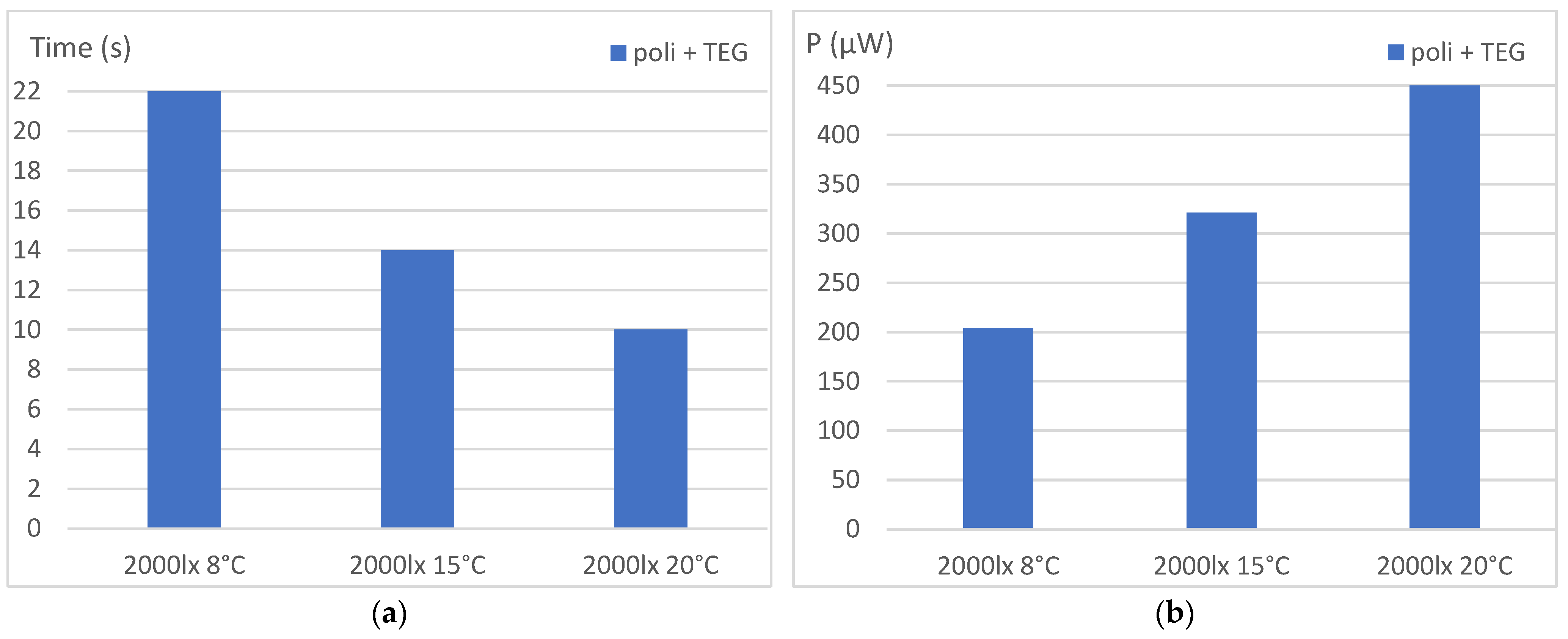
The concluding phase involved assessing the performance of the hybrid system where both the TEG and the PV panel charged the energy storage simultaneously. Each harvester would be connected to its own LTC3108 chip. In the experiment, a constant illumination value of 2000 lx was set and the temperature difference between the TEG cladding was changed. It was observed that for the smallest temperature difference at which the system with TEG starts, i.e., 8 °C, the capacitor charging time is the same as for the system with PV panel only and is 22 s. However, when the temperature gradient increases to 20 °C the supercapacitor is charged after only 10 s. If we consider the average power generated by the system, at the lowest temperature gradient it was 204 µW; at a difference of 15 °C, it was already 321 µW, while at the maximum difference of 20 °C, it was 450 µW. The results are presented in Figure 17.
4. Discussion and Conclusions
Three power systems were studied in Section 3: a single system with a thermoelectric harvester (TEG), a single system with a polycrystalline PV panel, and a hybrid system incorporating both simultaneously. The aggregate data are shown in Table 2. Since the systems have different dimensions, surface power density is a suitable parameter for comparing their generating capabilities. To evaluate the conversion efficiency of the management system, power and power density were given for the operation of the harvester in matching and at the output of the power system. Analyzing the data, we can see that the performance of the power-matched harvester (column 3 and 4) is mainly affected by ambient conditions. On the other hand, the operation of the full power system is tremendously influenced by the processing efficiency of the LTC3108 chip (column 5 and 6). For a system with a TEG, we observe relative match and the conversion efficiency ranges from 8 to 34%. For a single circuit with a PV panel, there are significant losses in converting power to the desired voltage level. For this system, the conversion efficiency for all cases is below 1%. This proves that the LTC3108 circuit did achieve adequate impedance matching for the selected panel at the selected light intensity.
In summary, the work focused on the construction and testing of a power system utilizing a 65 × 65 mm polycrystalline photovoltaic panel and a 40 × 40 mm thermoelectric generator. Each of the harvesters was equipped with its own LTC3108 energy management circuit and charged an energy buffer which was a 1 mF super capacitor. This circuit generated a steady power in the range of 205 to 450 µW. Testing revealed that the power system begins to function optimally when the light intensity exceeds 1000 lx and the temperature difference between the thermoelectric generator facings is at least 8 °C. A critical observation was the importance of properly choosing the energy conversion system; if the impedance of the harvester is not matched, there is a risk of losing almost all the power generated by one type of harvester. Remarkably, despite the very low efficiency of the hybrid system, the minimum value of generated power is 205 µW, which is 21.6 J per day. For optimal performance, the capacity of the energy buffer must be increased to 4.5 F. Additionally, the hybrid system ensures minimum power generation largely independent of operating conditions.
The selected harvesters are characterized by the fact that they both generate direct current and have no moving parts, which greatly facilitates their physical installation. The advantages of systems using solar panels include a relatively high surface power density; in addition, increasing the surface area of the panels linearly increases the generated power. The disadvantages of these systems include the need for illumination and change of internal resistance with a change in lighting, which forces the appropriate selection of energy conversion circuits to obtain satisfactory efficiency. Single systems based on the TEG have a much lower surface power density than solar panels, require a continuous temperature difference of the cladding, which forces a cooling system based on radiators and this adversely increases the size and weight of the system. However, they can operate without access to light and their internal resistance does not change with a change of temperature gradient. Considering this factor and the experimental results, the hybrid system utilizing a polycrystalline panel and a thermoelectric generator, offers a complementary operation in two ranges. When the temperature difference of the TEG plates is low, the energy that is transferred to the energy buffer comes from the solar panel, while when dT is high the output energy comes mainly from TEG.
The next phase of research involves creating our duplicator and voltage regulator tailored for the PV system, as depicted in Figure 2 and Figure 3. This should notably enhance the system’s overall efficiency. Currently, the TEG and solar panel are positioned adjacently. A compact design where the solar panel heats the TEG’s warm side during operation is the subsequent step to boost the power output. Post testing, these circuits will integrate into a wearable IoT node that employs a nRF52 family communication chip, aiming to monitor presence and location of persons within a facility. Moreover, this device could prolong the lifespan of the stress-monitoring node in steel infrastructures, as discussed in the author’s prior work [58]. This node currently utilizes a PIC 24FV family controller. Future research will also explore the operation of IoT nodes powered by energy harvesting as network components, using specialized verification and validation methods [59,60].
Funding
This publication was created thanks to a grant from the Scientific Council for the Discipline Automatic Control, Electronics, Electrical Engineering and Space Technology of the Warsaw University of Technology.
Data Availability Statement
Not applicable.
Conflicts of Interest
The author declares no conflict of interest.
References
- Kolcun, R.; Popescu, D.A.; Safronov, V.; Yadav, P.; Mandalari, A.M.; Mortier, R.; Haddadi, H. Revisiting IoT Device Identification. arXiv 2021, arXiv:2107.07818. [Google Scholar]
- Yin, F.; Yang, L.; Wang, Y.; Dai, J. IoT ETEI: End-to-End IoT Device Identification Method. In Proceedings of the 2021 IEEE Conference on Dependable and Secure Computing (DSC), Fukushima, Japan, 30 January–2 February 2021; pp. 1–8. [Google Scholar]
- Salman, O.; Elhajj, I.H.; Chehab, A.; Kayssi, A. A Machine Learning Based Framework for IoT Device Identification and Abnormal Traffic Detection. Trans. Emerg. Telecommun. Technol. 2022, 33, e3743. [Google Scholar] [CrossRef]
- Luong, N.C.; Hoang, D.T.; Wang, P.; Niyato, D.; Kim, D.I.; Han, Z. Data Collection and Wireless Communication in Internet of Things (IoT) Using Economic Analysis and Pricing Models: A Survey. IEEE Commun. Surv. Tutor. 2016, 18, 2546–2590. [Google Scholar] [CrossRef]
- Pawar, P.; Trivedi, A. Device-to-Device Communication Based IoT System: Benefits and Challenges. IETE Tech. Rev. 2019, 36, 362–374. [Google Scholar] [CrossRef]
- Taami, T.; Azizi, S.; Yarinezhad, R. An Efficient Route Selection Mechanism Based on Network Topology in Battery-Powered Internet of Things Networks. Peer-Peer Netw. Appl. 2023, 16, 450–465. [Google Scholar] [CrossRef]
- Lee, J.; Choi, S.; Kim, D.; Choi, Y.; Sun, W. A Novel Hardware Security Architecture for IoT Device: PD-CRP (PUF Database and Challenge–Response Pair) Bloom Filter on Memristor-Based PUF. Appl. Sci. 2020, 10, 6692. [Google Scholar] [CrossRef]
- Cai, T.; Ma, Y.; Liu, P.; Niu, D.; Li, L. A New NVM Device Driver for IoT Time Series Database. Micromachines 2022, 13, 385. [Google Scholar] [CrossRef]
- Lavalle, A.; Teruel, M.A.; Maté, A.; Trujillo, J. Improving Sustainability of Smart Cities through Visualization Techniques for Big Data from IoT Devices. Sustainability 2020, 12, 5595. [Google Scholar] [CrossRef]
- Jecan, E.; Pop, C.; Ratiu, O.; Puschita, E. Predictive Energy-Aware Routing Solution for Industrial IoT Evaluated on a WSN Hardware Platform. Sensors 2022, 22, 2107. [Google Scholar] [CrossRef]
- Usman, N.; Alfandi, O.; Usman, S.; Khattak, A.M.; Awais, M.; Hayat, B.; Sajid, A. An Energy Efficient Routing Approach for IoT Enabled Underwater WSNs in Smart Cities. Sensors 2020, 20, 4116. [Google Scholar] [CrossRef]
- Poornima, M.R.; Vimala, H.S.; Shreyas, J. Holistic Survey on Energy Aware Routing Techniques for IoT Applications. J. Netw. Comput. Appl. 2023, 213, 103584. [Google Scholar] [CrossRef]
- Häggström, F.; Delsing, J. IoT Energy Storage—A Forecast. Energy Harvest. Syst. 2018, 5, 43–51. [Google Scholar] [CrossRef]
- Krishna, G.; Singh, R.; Gehlot, A.; Akram, S.V.; Priyadarshi, N.; Twala, B. Digital Technology Implementation in Battery-Management Systems for Sustainable Energy Storage: Review, Challenges, and Recommendations. Electronics 2022, 11, 2695. [Google Scholar] [CrossRef]
- Liu, L.; Guo, X.; Liu, W.; Lee, C. Recent Progress in the Energy Harvesting Technology—From Self-Powered Sensors to Self-Sustained IoT, and New Applications. Nanomaterials 2021, 11, 2975. [Google Scholar] [CrossRef] [PubMed]
- Kjellby, R.A.; Cenkeramaddi, L.R.; Frøytlog, A.; Lozano, B.B.; Soumya, J.; Bhange, M. Long-Range & Self-Powered IoT Devices for Agriculture & Aquaponics Based on Multi-Hop Topology. In Proceedings of the 2019 IEEE 5th World Forum on Internet of Things (WF-IoT), Limerick, Ireland, 15–18 April 2019; pp. 545–549. [Google Scholar]
- Xiao, H.; Qi, N.; Yin, Y.; Yu, S.; Sun, X.; Xuan, G.; Liu, J.; Xiao, S.; Li, Y.; Li, Y. Investigation of Self-Powered IoT Sensor Nodes for Harvesting Hybrid Indoor Ambient Light and Heat Energy. Sensors 2023, 23, 3796. [Google Scholar] [CrossRef]
- Dziadak, B.; Kucharek, M.; Starzyński, J. Powering the WSN Node for Monitoring Rail Car Parameters, Using a Piezoelectric Energy Harvester. Energies 2022, 15, 1641. [Google Scholar] [CrossRef]
- Sharma, S.; Kiran, R.; Azad, P.; Vaish, R. A Review of Piezoelectric Energy Harvesting Tiles: Available Designs and Future Perspective. Energy Convers. Manag. 2022, 254, 115272. [Google Scholar] [CrossRef]
- Maharjan, P.; Lee, S.; Bhatta, T.; Pradhan, G.B.; Shrestha, K.; Jeong, S.; Rana, S.S.; Park, J.Y. A 3D Printed Compact and Intelligent Power Module Based on Vibration Energy Harvester Integrated with Self-Powered Triboelectric Sensor for Industry 4.0 IoT Applications. Adv. Mater. Technol. 2023, 8, 2201545. [Google Scholar] [CrossRef]
- Zou, Y.; Sun, M.; Yan, F.; Du, T.; Xi, Z.; Li, F.; Zhu, C.; Wang, H.; Zhao, J.; Sun, P.; et al. A High-Performance Flag-Type Triboelectric Nanogenerator for Scavenging Wind Energy toward Self-Powered IoTs. Materials 2022, 15, 3696. [Google Scholar] [CrossRef]
- Yaşar, O.; Uluşan, H.; Zorlu, Ö.; Şardan-Sukas, Ö.; Külah, H. Optimization of AA-Battery Sized Electromagnetic Energy Harvesters: Reducing the Resonance Frequency Using a Non-Magnetic Inertial Mass. IEEE Sens. J. 2018, 18, 4509–4516. [Google Scholar] [CrossRef]
- Dinulovic, D.; Shousha, M.; Al-Batol, M.; Zafar, T.; Bickel, J.; Ngo, H.-D.; Haug, M. Dual-Rotor Electromagnetic-Based Energy Harvesting System for Smart Home Applications. IEEE Trans. Magn. 2021, 57, 1–5. [Google Scholar] [CrossRef]
- Dziadak, B.; Makowski, Ł.; Kucharek, M.; Jóśko, A. Energy Harvesting for Wearable Sensors and Body Area Network Nodes. Energies 2023, 16, 1681. [Google Scholar] [CrossRef]
- Machacek, Z.; Sotola, V.; Petras, R.; Schneider, M.; Masny, Z.; Idzkowski, A.; Walendziuk, W. Advanced Energy Harvesting from Heating for a Water Consumption Meter. Proceedings 2020, 51, 21. [Google Scholar] [CrossRef]
- Chang, T.; Rincón-Mora, G.A. Fast Energy-Harvesting TEG-Supplied Charging Regulator Microsystem. IEEE Trans. Power Electron. 2023, 38, 9116–9126. [Google Scholar] [CrossRef]
- Lee, Y.C.; Ramiah, H.; Choo, A.; Churchill, K.K.P.; Lai, N.S.; Lim, C.C.; Chen, Y.; Mak, P.-I.; Martins, R.P. High-Performance Multiband Ambient RF Energy Harvesting Front-End System for Sustainable IoT Applications—A Review. IEEE Access 2023, 11, 11143–11164. [Google Scholar] [CrossRef]
- Ahmad, F.F.; Ghenai, C.; Bettayeb, M. Maximum Power Point Tracking and Photovoltaic Energy Harvesting for Internet of Things: A Comprehensive Review. Sustain. Energy Technol. Assess. 2021, 47, 101430. [Google Scholar] [CrossRef]
- Mondal, S.; Paily, R. On-Chip Photovoltaic Power Harvesting System with Low-Overhead Adaptive MPPT for IoT Nodes. IEEE Internet Things J. 2017, 4, 1624–1633. [Google Scholar] [CrossRef]
- Páez-Montoro, A.; García-Valderas, M.; Olías-Ruíz, E.; López-Ongil, C. Solar Energy Harvesting to Improve Capabilities of Wearable Devices. Sensors 2022, 22, 3950. [Google Scholar] [CrossRef]
- Mahdi Elsiddig Haroun, F.; Mohamad Deros, S.N.; Ahmed Alkahtani, A.; Md Din, N. Towards Self-Powered WSN: The Design of Ultra-Low-Power Wireless Sensor Transmission Unit Based on Indoor Solar Energy Harvester. Electronics 2022, 11, 2077. [Google Scholar] [CrossRef]
- Goldsmid, H.J. Introduction to Thermoelectricity; Springer Series in Materials Science; Springer: Berlin/Heidelberg, Germany, 2010; Volume 121, ISBN 978-3-642-00715-6. [Google Scholar]
- Hasan, M.d.N.; Nafea, M.; Nayan, N.; Mohamed Ali, M.S. Thermoelectric Generator: Materials and Applications in Wearable Health Monitoring Sensors and Internet of Things Devices. Adv. Mater. Technol. 2022, 7, 2101203. [Google Scholar] [CrossRef]
- Pourkiaei, S.M.; Ahmadi, M.H.; Sadeghzadeh, M.; Moosavi, S.; Pourfayaz, F.; Chen, L.; Pour Yazdi, M.A.; Kumar, R. Thermoelectric Cooler and Thermoelectric Generator Devices: A Review of Present and Potential Applications, Modeling and Materials. Energy 2019, 186, 115849. [Google Scholar] [CrossRef]
- Kishore, R.A.; Priya, S. A Review on Low-Grade Thermal Energy Harvesting: Materials, Methods and Devices. Materials 2018, 11, 1433. [Google Scholar] [CrossRef] [PubMed]
- Chen, C.J. Physics of Solar Energy; Wiley: Hoboken, NJ, USA, 2011. [Google Scholar]
- Sredensek, K.; Sem, S. Parameter Determination of a Solar Cell Model Using Differential Evolution Algorithm. Przegląd Elektrotechniczny 2019, 1, 167–170. [Google Scholar] [CrossRef]
- Araújo, N.M.F.T.S.; Sousa, F.J.P.; Costa, F.B. Equivalent Models for Photovoltaic Cell—A Review. Reterm 2020, 19, 77. [Google Scholar] [CrossRef]
- Shockley, W.; Queisser, H.J. Detailed Balance Limit of Efficiency of P-n Junction Solar Cells. J. Appl. Phys. 1961, 32, 510–519. [Google Scholar] [CrossRef]
- Rühle, S. Tabulated Values of the Shockley–Queisser Limit for Single Junction Solar Cells. Sol. Energy 2016, 130, 139–147. [Google Scholar] [CrossRef]
- Yoon, S.; Tak, S.; Kim, J.; Jun, Y.; Kang, K.; Park, J. Application of Transparent Dye-Sensitized Solar Cells to Building Integrated Photovoltaic Systems. Build. Environ. 2011, 46, 1899–1904. [Google Scholar] [CrossRef]
- Tonui, P.; Oseni, S.O.; Sharma, G.; Yan, Q.; Tessema Mola, G. Perovskites Photovoltaic Solar Cells: An Overview of Current Status. Renew. Sustain. Energy Rev. 2018, 91, 1025–1044. [Google Scholar] [CrossRef]
- Zhou, D.; Zhou, T.; Tian, Y.; Zhu, X.; Tu, Y. Perovskite-Based Solar Cells: Materials, Methods, and Future Perspectives. J. Nanomater. 2018, 2018, e8148072. [Google Scholar] [CrossRef]
- Roldán-Carmona, C.; Malinkiewicz, O.; Soriano, A.; Mínguez Espallargas, G.; Garcia, A.; Reinecke, P.; Kroyer, T.; Dar, M.I.; Nazeeruddin, M.K.; Bolink, H.J. Flexible High Efficiency Perovskite Solar Cells. Energy Environ. Sci. 2014, 7, 994. [Google Scholar] [CrossRef]
- Rong, Y.; Hu, Y.; Mei, A.; Tan, H.; Saidaminov, M.I.; Seok, S.I.; McGehee, M.D.; Sargent, E.H.; Han, H. Challenges for Com-mercializing Perovskite Solar Cells. Science 2018, 361, eaat8235. [Google Scholar] [CrossRef] [PubMed]
- Yamaguchi, M.; Dimroth, F.; Geisz, J.F.; Ekins-Daukes, N.J. Multi-Junction Solar Cells Paving the Way for Super High-Efficiency. J. Appl. Phys. 2021, 129, 240901. [Google Scholar] [CrossRef]
- Chang, M.-C.; Liu, S.-I. An Indoor Photovoltaic Energy Harvester Using Time-Based MPPT and on-Chip Photovoltaic Cell. IEEE Trans. Circuits Syst. II Express Briefs 2020, 67, 2432–2436. [Google Scholar] [CrossRef]
- Ibrahim, M.H.; Ang, S.P.; Dani, M.N.; Rahman, M.I.; Petra, R.; Sulthan, S.M. Optimizing Step-Size of Perturb & Observe and Incremental Conductance MPPT Techniques Using PSO for Grid-Tied PV System. IEEE Access 2023, 11, 13079–13090. [Google Scholar] [CrossRef]
- Michalski, A.; Watral, Z. Problems of Powering End Devices in Wireless Networks of the Internet of Things. Energies 2021, 14, 2417. [Google Scholar] [CrossRef]
- Michalski, A.; Dziadak, B.; Makowski, Ł. Survey of Energy Harvesting Systems for Wireless Sensor Networks in Environmental Monitoring. Metrol. Meas. Syst. 2016, 23, 495–512. [Google Scholar]
- Kramer, L.R.; Maran, A.L.O.; de Souza, S.S.; Ando Junior, O.H. Analytical and Numerical Study for the Determination of a Thermoelectric Generator’s Internal Resistance. Energies 2019, 12, 3053. [Google Scholar] [CrossRef]
- Mathews, I.; King, P.J.; Stafford, F.; Frizzell, R. Performance of III–V Solar Cells as Indoor Light Energy Harvesters. IEEE J. Photovolt. 2016, 6, 230–235. [Google Scholar] [CrossRef]
- De Rossi, F.; Pontecorvo, T.; Brown, T.M. Characterization of Photovoltaic Devices for Indoor Light Harvesting and Customization of Flexible Dye Solar Cells to Deliver Superior Efficiency under Artificial Lighting. Appl. Energy 2015, 156, 413–422. [Google Scholar] [CrossRef]
- El-Shaer, A.; Tadros, M.T.Y.; Khalifa, M. Effect of Light Intensity and Temperature on Crystalline Silicon Solar Modules Parameters. Int. J. Emerg. Technol. Adv. Eng. 2014, 4, 2014. [Google Scholar]
- Mulcué-Nieto, L.F.; Echeverry-Cardona, L.F.; Restrepo-Franco, A.M.; García-Gutiérrez, G.A.; Jiménez-García, F.N.; Mora-López, L. Energy Performance Assessment of Monocrystalline and Polycrystalline Photovoltaic Modules in the Tropical Mountain Climate: The Case for Manizales-Colombia. Energy Rep. 2020, 6, 2828–2835. [Google Scholar] [CrossRef]
- LTC3108 Datasheet and Product Info|Analog Devices. Available online: https://www.analog.com/en/products/ltc3108.html#product-overview (accessed on 3 September 2023).
- Dziadak, B.; Makowski, L.; Michalski, A. Konstrukcja Węzła Bezprzewodowej Sieci Czujnikowej Wykorzystującego Energy Harvesting. Przegląd Elektrotechniczny 2016, 1, 65–68. [Google Scholar] [CrossRef]
- Dziadak, B. Structural Health Monitoring System for Snow and Wind Load Measurement. Electronics 2020, 9, 609. [Google Scholar] [CrossRef]
- Krichen, M. A Survey on Formal Verification and Validation Techniques for Internet of Things. Appl. Sci. 2023, 13, 8122. [Google Scholar] [CrossRef]
- Souri, A.; Norouzi, M. A State-of-the-Art Survey on Formal Verification of the Internet of Things Applications. J. Serv. Sci. Res. 2019, 11, 47–67. [Google Scholar] [CrossRef]
Figure 1.
Structure of a single p–n junction in a thermoelectric generator.
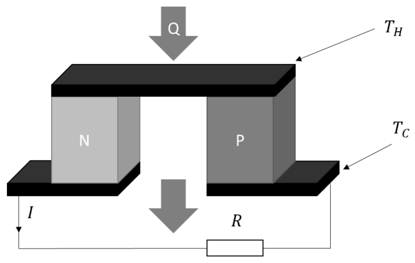
Figure 2.
Charge pump: (a) an exponential charge pump and, (b) a Dickson charge pump.

Figure 3.
Schematic of a voltage booster circuit with a transformer.

Figure 4.
Electrical model of a solar cell.
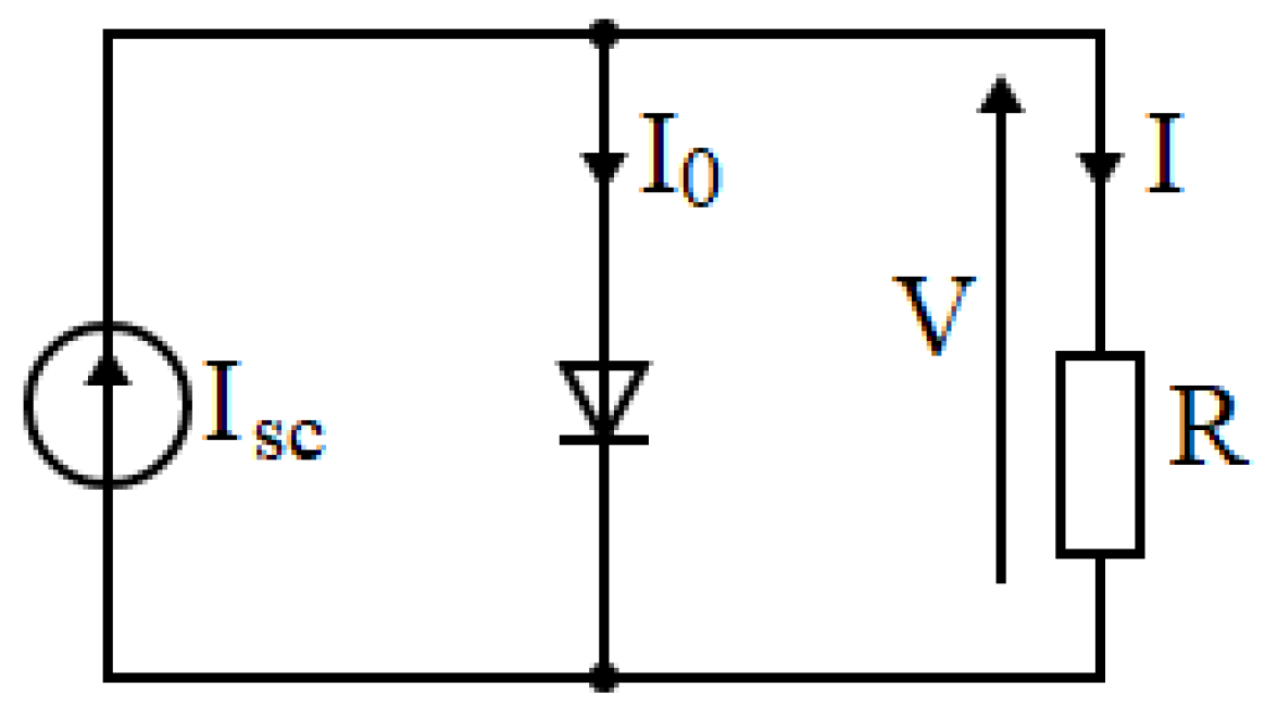
Figure 5.
Solar cell generations.
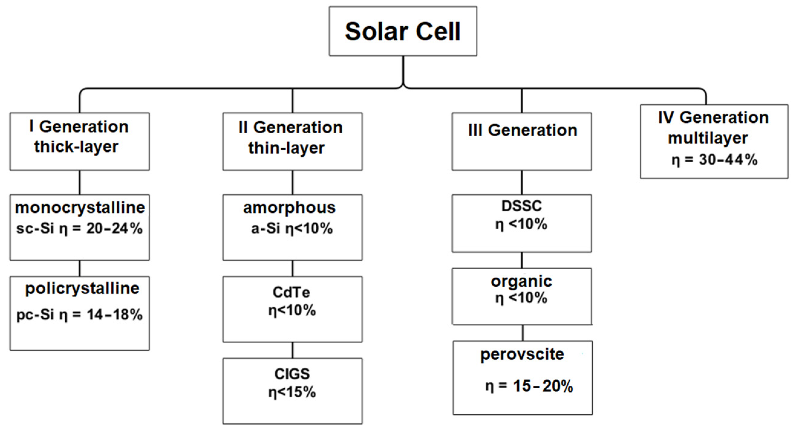
Figure 6.
Solar energy conversion system.
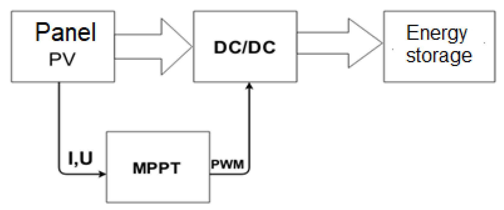
Figure 7.
Tested harvester.
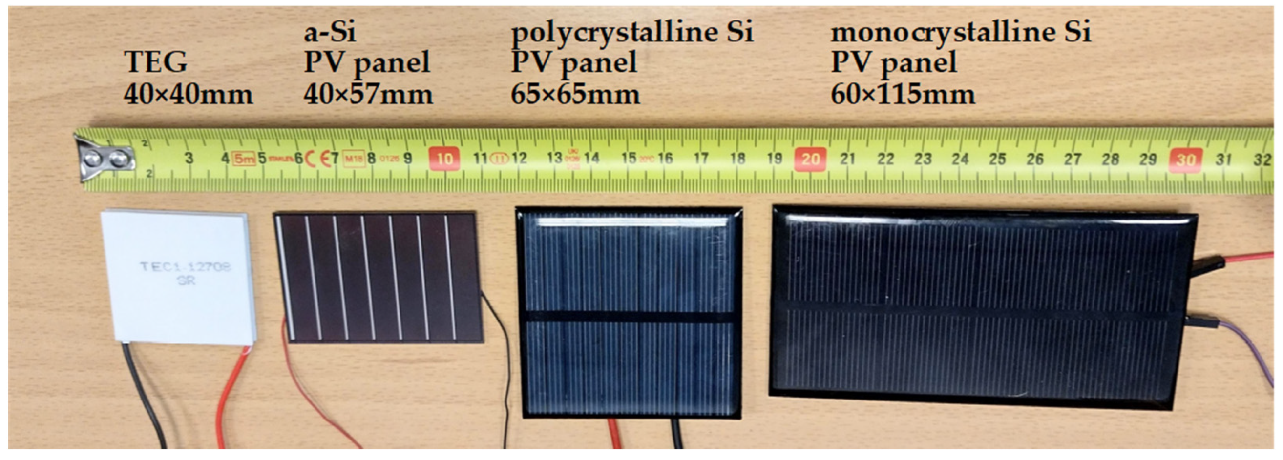
Figure 8.
Thermoelectric generator under test.

Figure 9.
Power generated by the TEG as a function of load resistance for 4 temperature gradients.
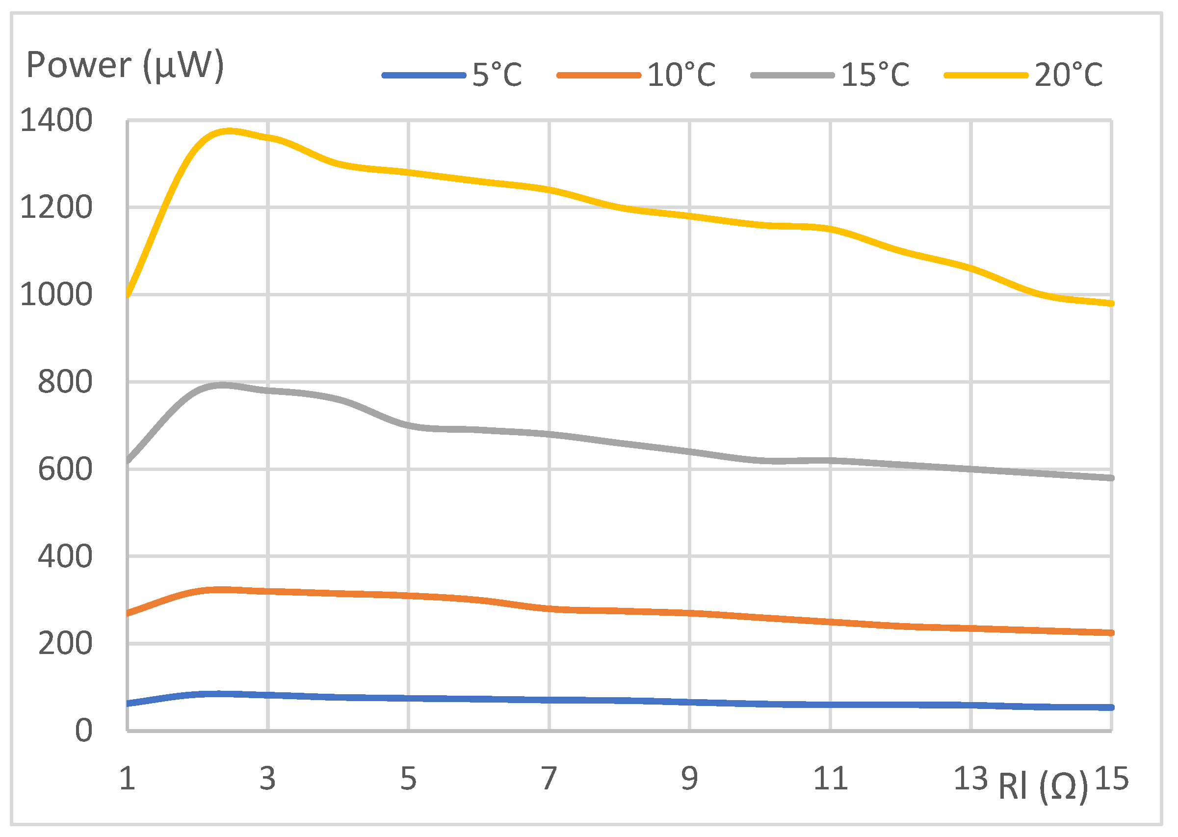
Figure 10.
Power generated as a function of temperature gradient.
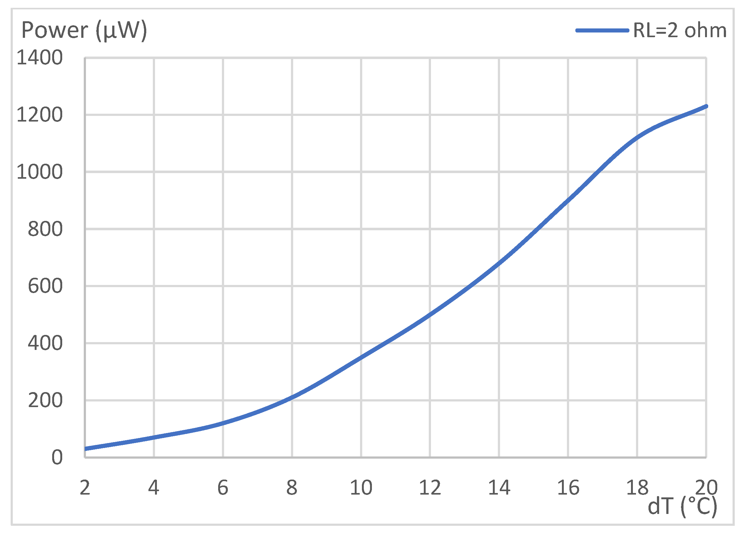
Figure 11.
Measurement stand for determining the parameters of a solar cell.
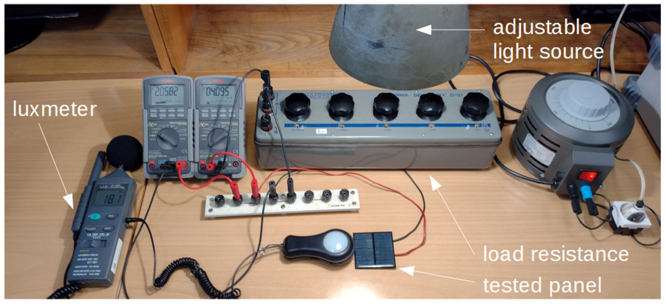
Figure 12.
Load characteristics for three solar cells at different light intensities.
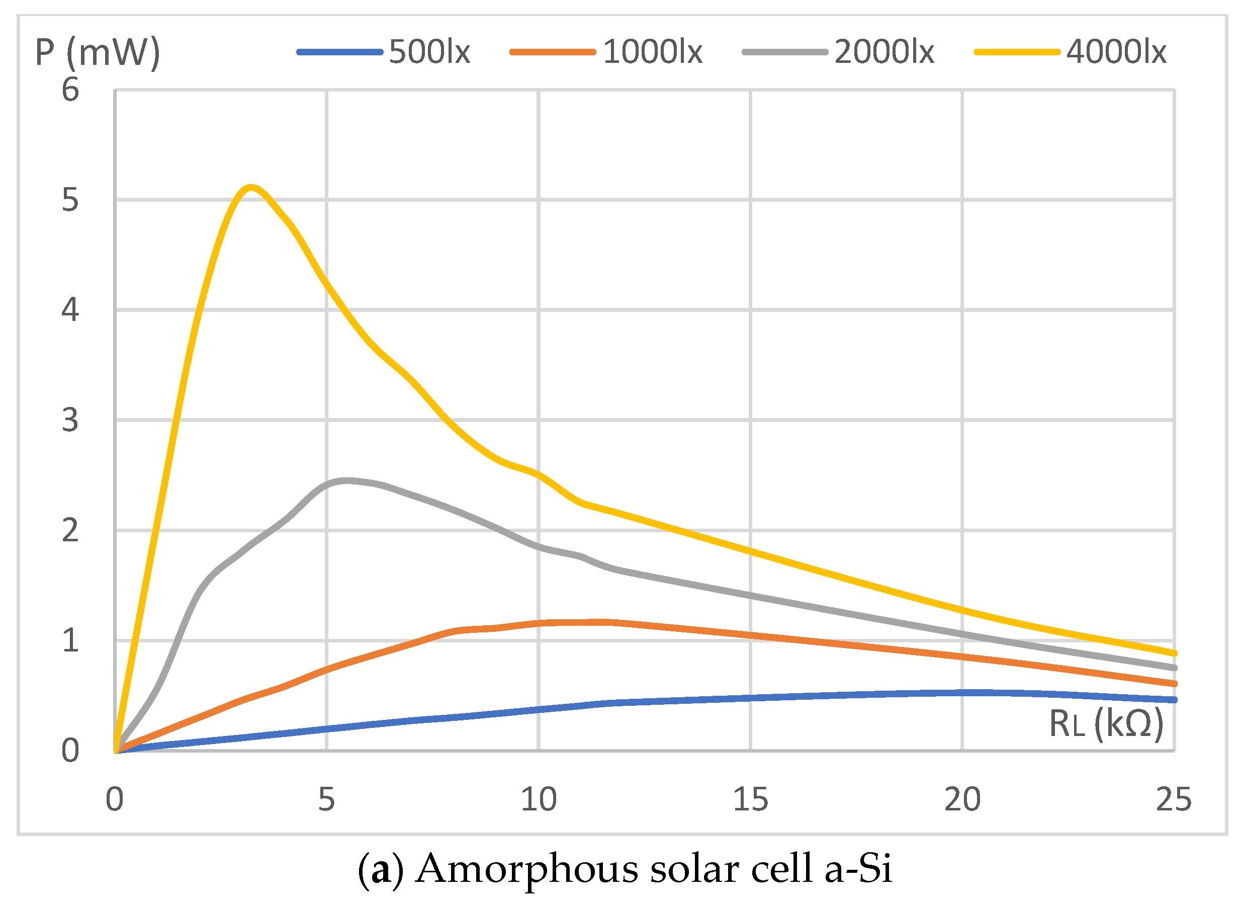
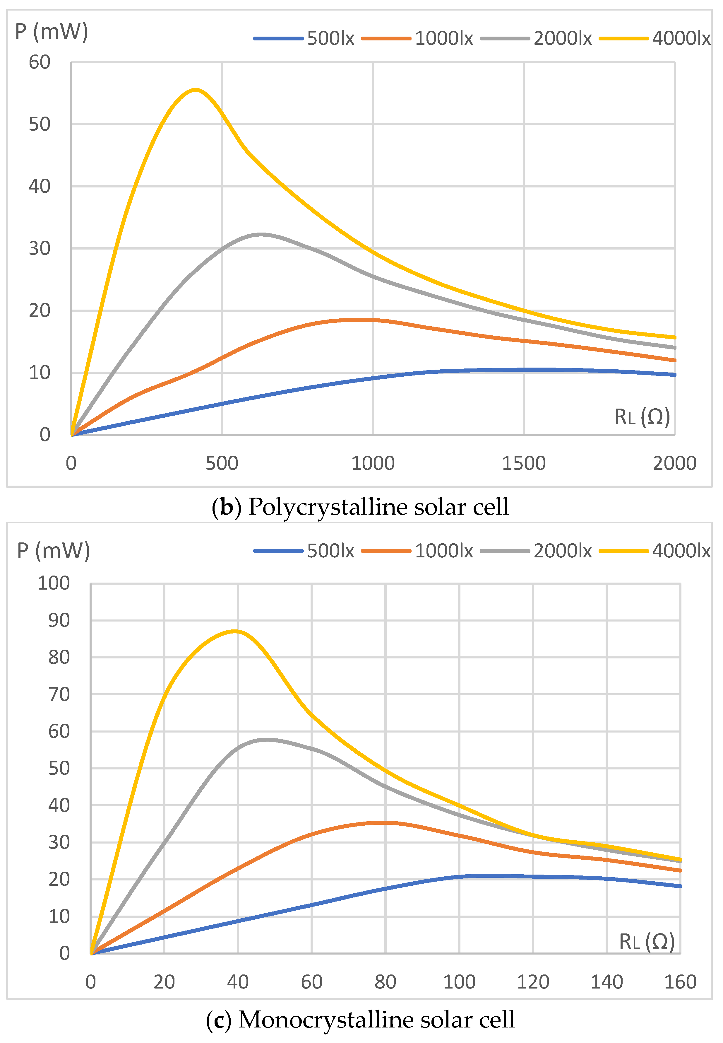
Figure 13.
Power generation for three PV panels: (a) generated power in function illumination intensity and (b) power density in function illumination intensity.
Figure 13.
Power generation for three PV panels: (a) generated power in function illumination intensity and (b) power density in function illumination intensity.
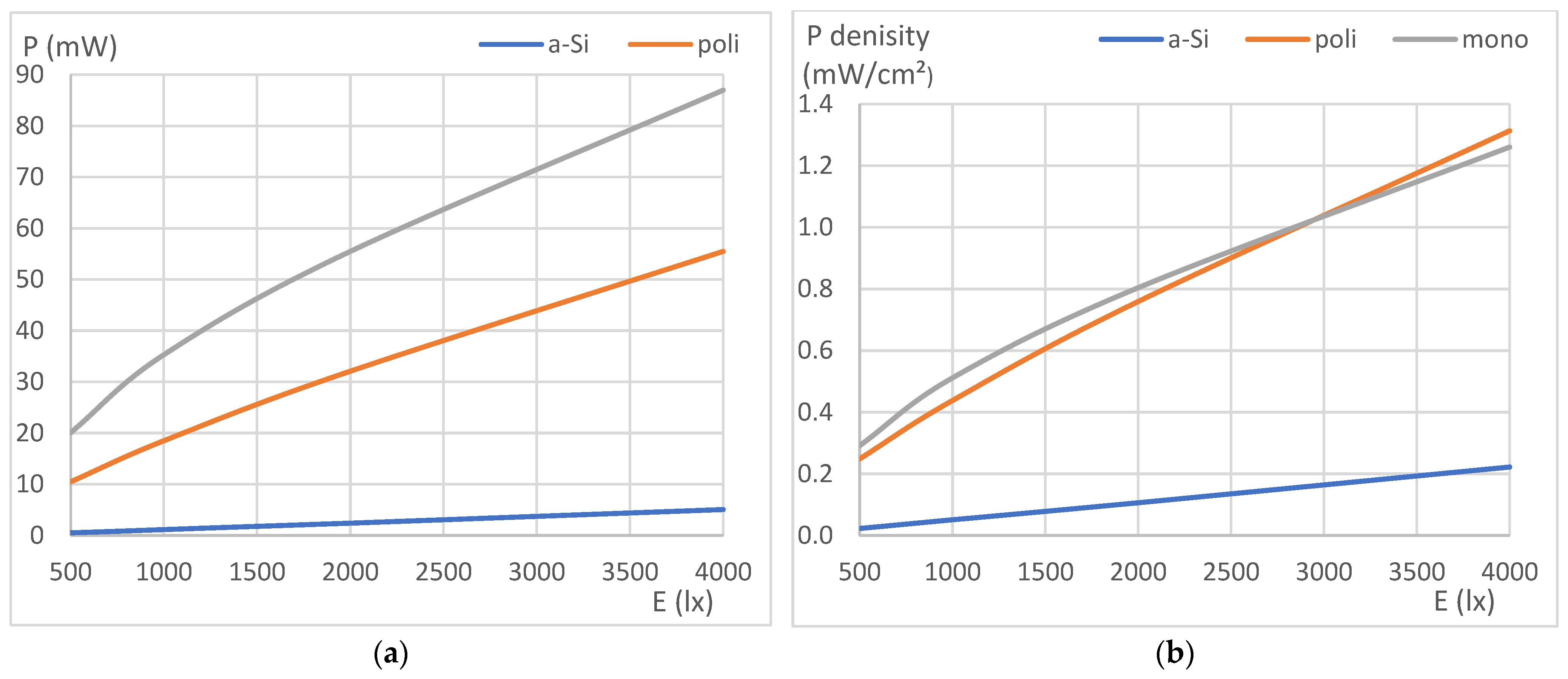
Figure 14.
Implemented LTC3108 controller circuit to work with the thermoelectric generator.
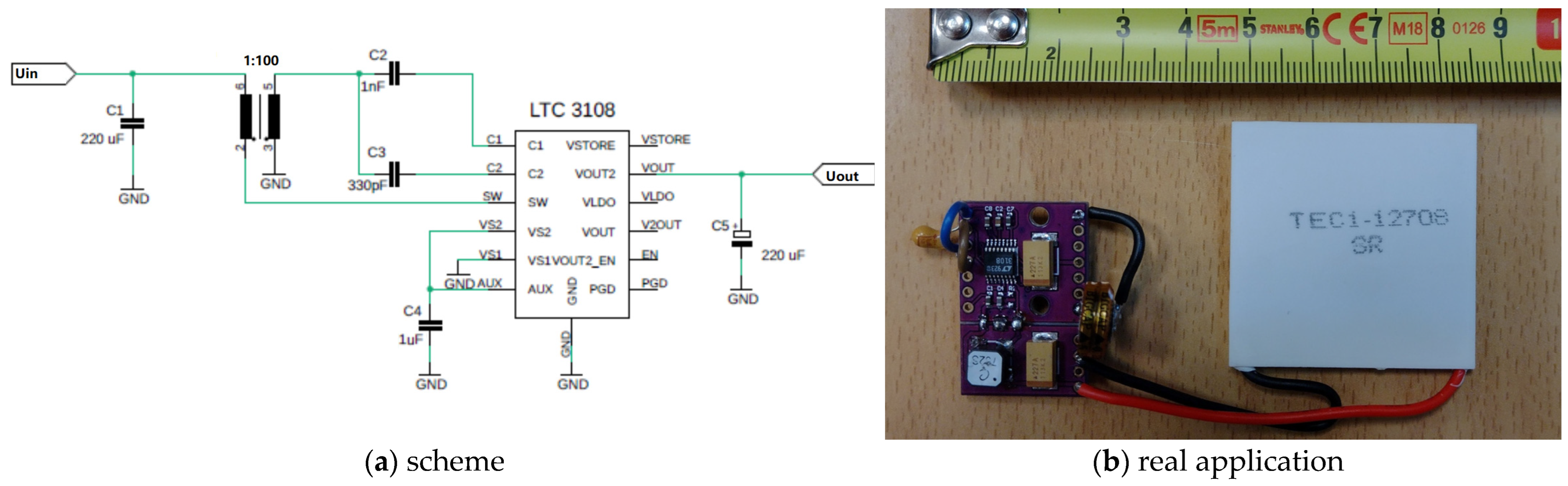
Figure 15.
Time required to harvest 4.5 mJ for a system with a TEG.
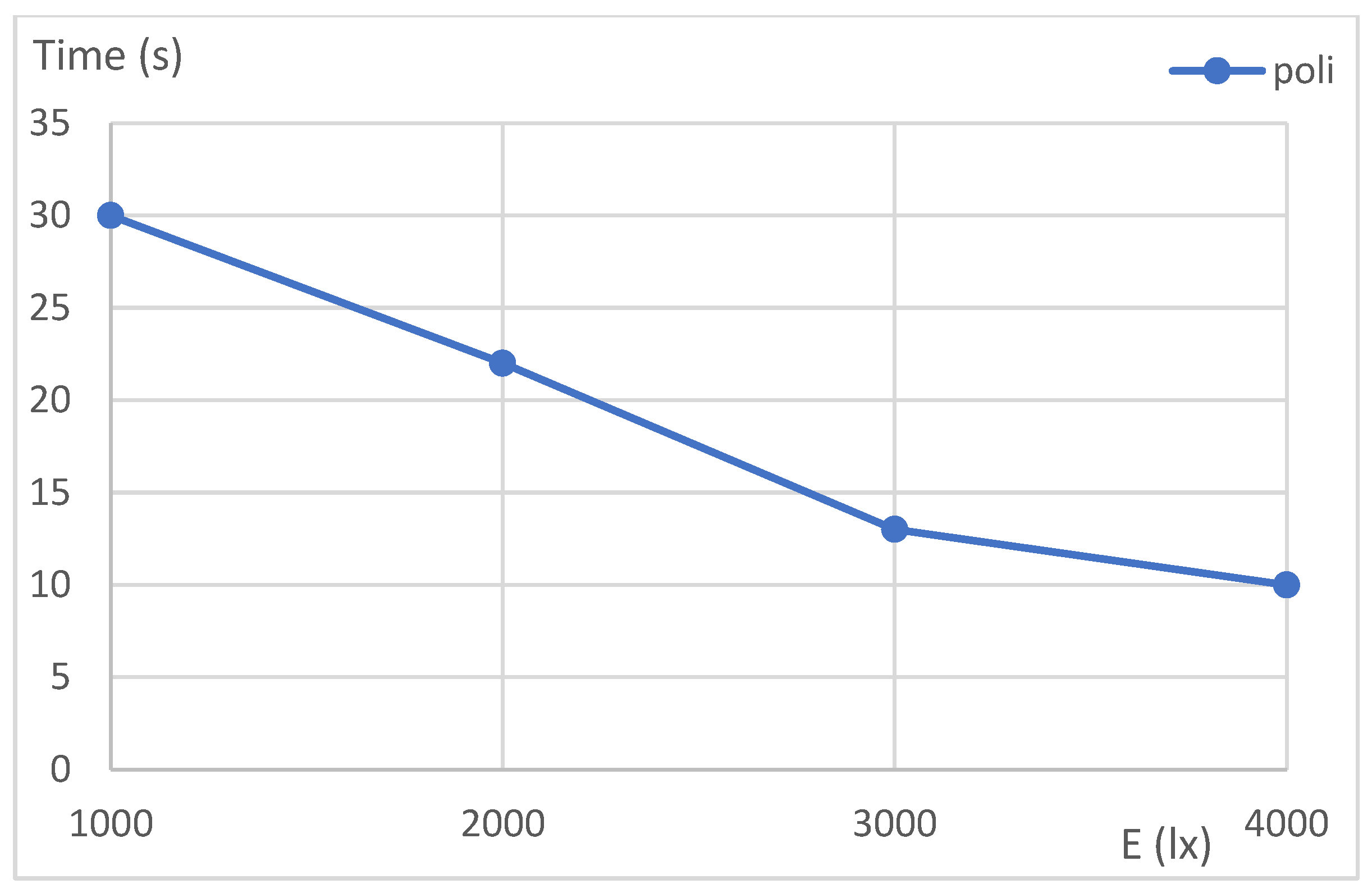
Figure 16.
Time required to harvest 4.5 mJ for a system with a PV panel.
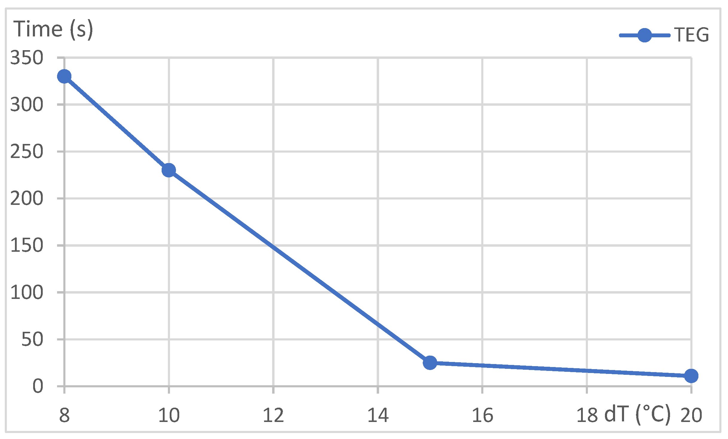
Figure 17.
Performance characteristics of the hybrid polymorphous PV panel and TEG unit for different operating conditions: (a) time required to harvest 4.5 mJ and (b) output power of the power system.
Figure 17.
Performance characteristics of the hybrid polymorphous PV panel and TEG unit for different operating conditions: (a) time required to harvest 4.5 mJ and (b) output power of the power system.

Table 1.
Parameters of energy storage for the IoT.
| Type of Energy Storage | Energy Density (Wh/kg) | Energy Density (Wh/L) | Self-Discharge Rate per Month | Cycle Life |
|---|---|---|---|---|
| Lithium-ion (Li-ion) batteries | 150–250 | 250–650 | 5% | 500–1500 |
| Lithium polymer (LiPo) batteries | 100–265 | 300–500 | 5% | 400–1200 |
| Nickel-metal hydride (NiMH) batteries | 60–120 | - | 20–30 | 500–2000 |
| Supercapacitors | 5–10 | 4–30 | 5–20% per day | >1,000,000 |
| Thin-film batteries | ~100 | - | ~0.5% | 1000 |
Table 2.
Energy parameters of single and hybrid power units.
| Type of EH | Conditions | Power of Harvester (mW) | Power Density of Harvester (µW/cm2) | Power of Power Unit (µW) | Power Density of Power Unit (µW/cm2) | Efficiency (%) |
|---|---|---|---|---|---|---|
| TEG | dT = 8 °C | 0.2 | 12.5 | 14 | 1 | 8.3 |
| TEG | dT = 15 °C | 0.8 | 50 | 180 | 11 | 22.0 |
| TEG | dT = 20 °C | 1.2 | 77 | 409 | 26 | 34.0 |
| poli | 1000 lx | 18.5 | 437 | 150 | 4 | 0.9 |
| poli | 2000 lx | 32.1 | 759 | 204 | 5 | 0.7 |
| poli | 4000 lx | 55.5 | 1313 | 409 | 10 | 0.8 |
| TEG + poli | 2000 lx dT = 8 °C | 32.4 | - | 205 | - | 0.6 |
| TEG + poli | 2000 lx dT = 15 °C | 32.9 | - | 321 | - | 1.0 |
| TEG + poli | 2000 lx dT = 20 °C | 33.3 | - | 450 | - | 1.4 |
Disclaimer/Publisher’s Note: The statements, opinions and data contained in all publications are solely those of the individual author(s) and contributor(s) and not of MDPI and/or the editor(s). MDPI and/or the editor(s) disclaim responsibility for any injury to people or property resulting from any ideas, methods, instructions or products referred to in the content. |
© 2023 by the author. Licensee MDPI, Basel, Switzerland. This article is an open access article distributed under the terms and conditions of the Creative Commons Attribution (CC BY) license (https://creativecommons.org/licenses/by/4.0/).
Share and Cite
MDPI and ACS Style
Dziadak, B. Hybrid Optical and Thermal Energy Conversion System to Power Internet of Things Nodes. Energies 2023, 16, 7076. https://doi.org/10.3390/en16207076
AMA Style
Dziadak B. Hybrid Optical and Thermal Energy Conversion System to Power Internet of Things Nodes. Energies. 2023; 16(20):7076. https://doi.org/10.3390/en16207076
Chicago/Turabian StyleDziadak, Bogdan. 2023. "Hybrid Optical and Thermal Energy Conversion System to Power Internet of Things Nodes" Energies 16, no. 20: 7076. https://doi.org/10.3390/en16207076
Note that from the first issue of 2016, this journal uses article numbers instead of page numbers. See further details here.