
Parameter Optimization Design of the Commutation Circuit of a Hybrid DC-Current-Limiting Circuit Breaker

Abstract
:1. Introduction
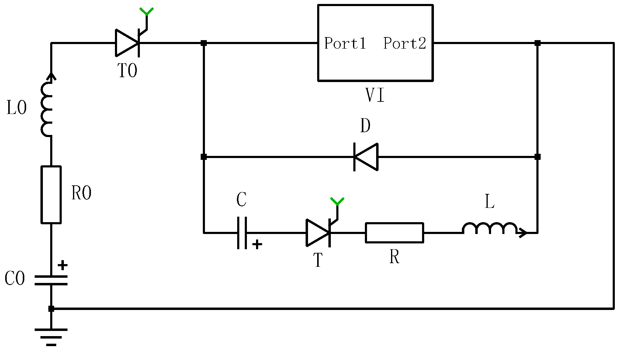
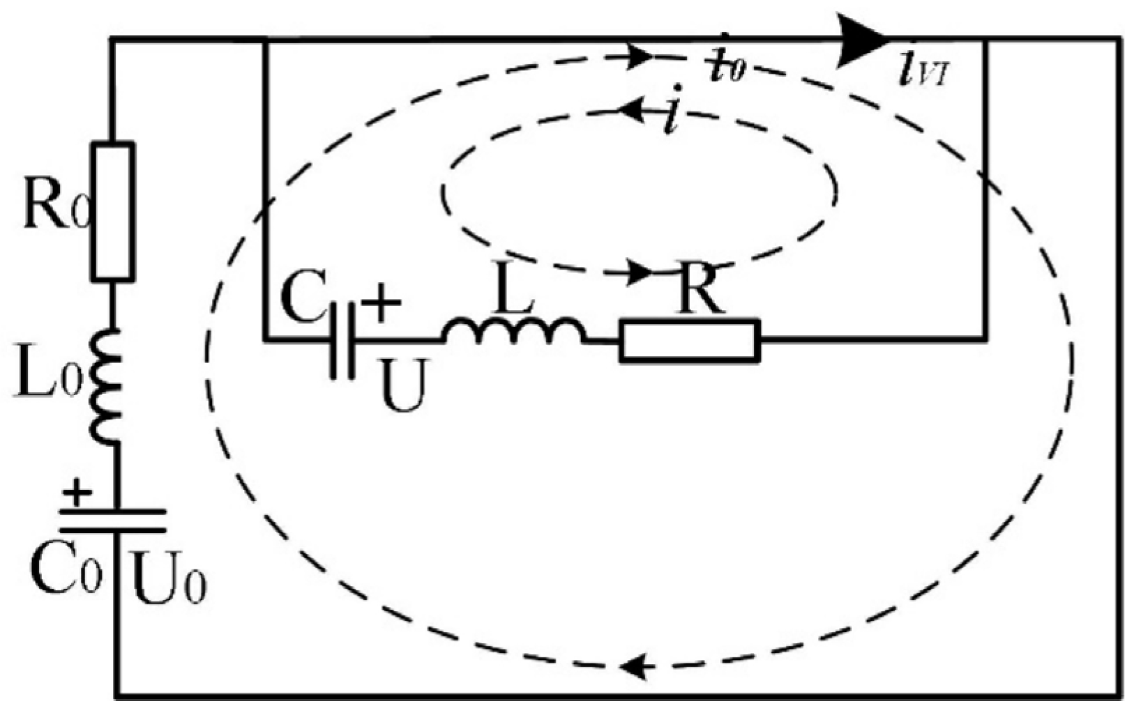
2. Operating Principle of the HDCCLCB
- (1)
- Under normal working conditions, the main circuit current flows through the vacuum interrupter (VI);
- (2)
- When the current needs to be cut off, the vacuum interrupter (VI) is opened, and the vacuum arc appears;
- (3)
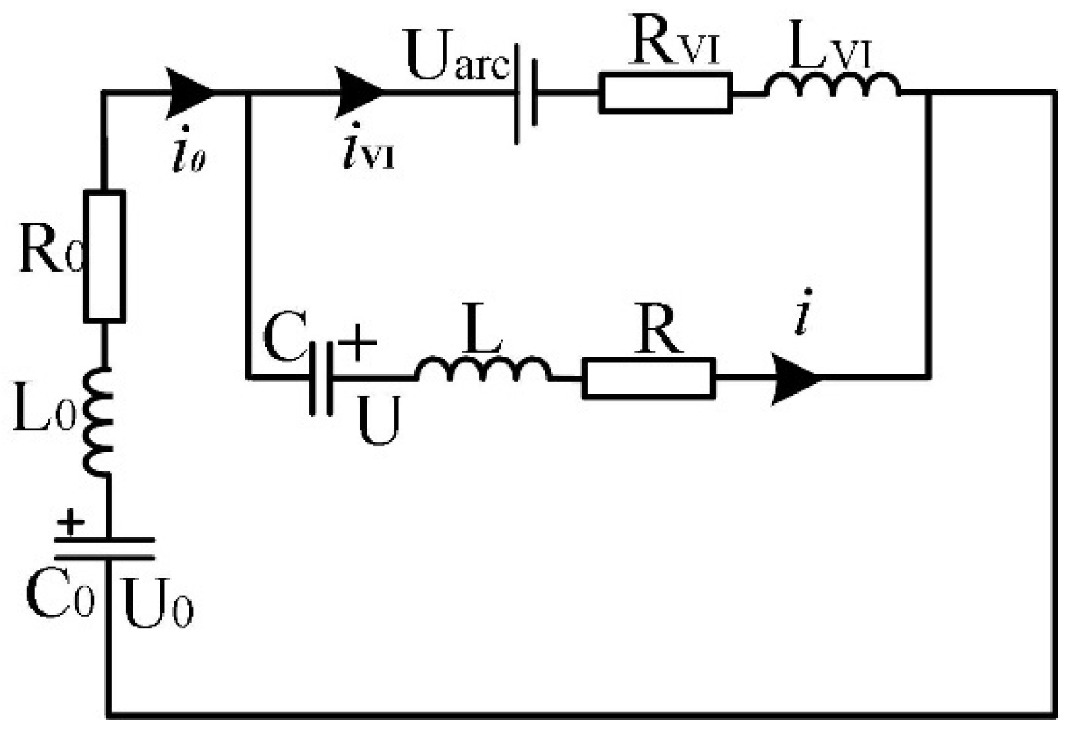
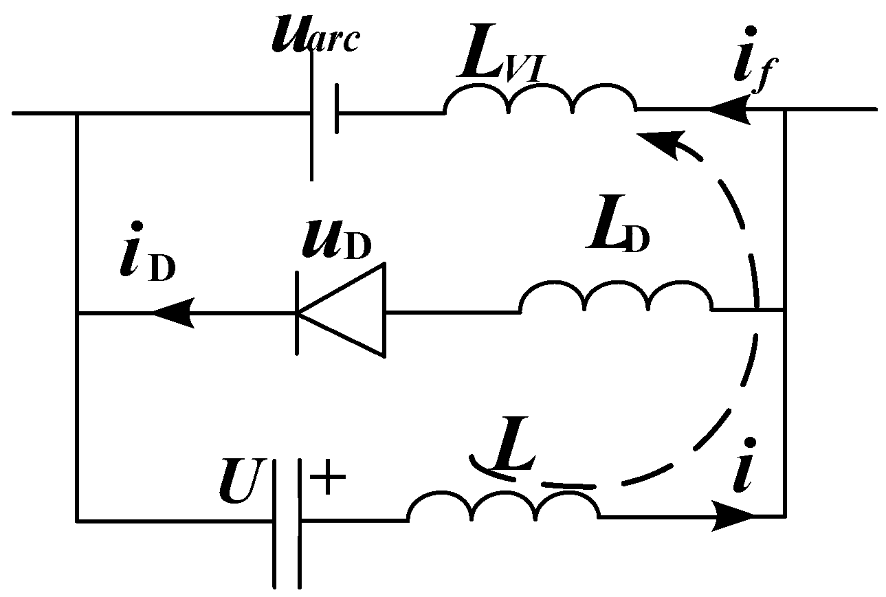
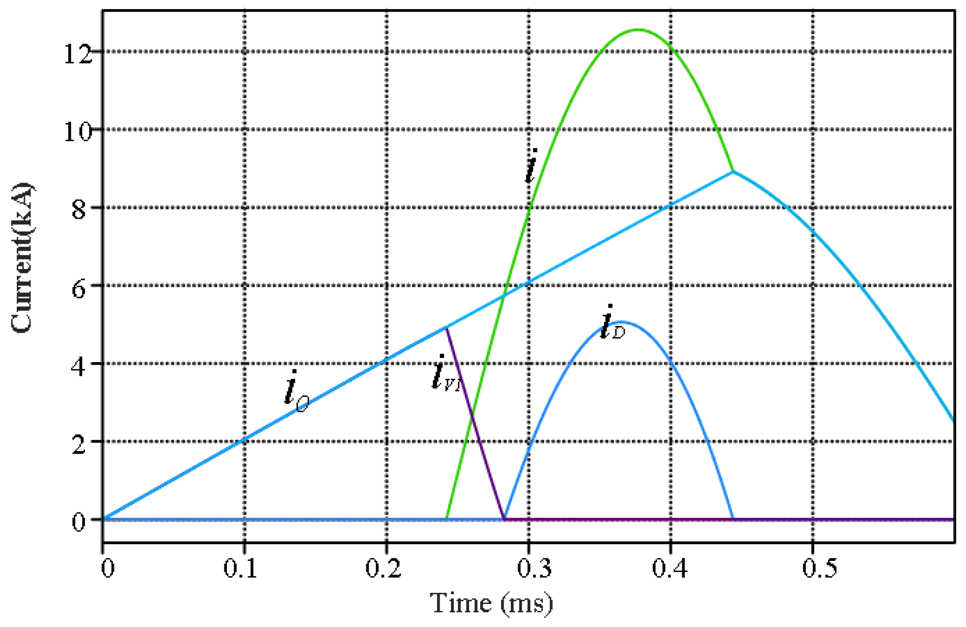
- After a short arcing time, the thyristor (T) of the commutation circuit is triggered, and the pre-charged capacitor (C) discharges the vacuum interrupter (VI) through the inductor (L). The reverse parallel diode (D) cannot be turned on due to the clamping effect of the arc voltage, so the entire pulse current flows to the VI. The pulse current is opposite to the main circuit current, which makes the current in the VI gradually decrease until the current zero crossing is formed;
- (4)
- Because the reverse pulse current flows through the reverse parallel diode (D) after the arc is extinguished, the voltage drop on the contact of the VI is approximately zero. The transient recovery overvoltage will not occur until the pulse current is equal to the main circuit current again. During this phase, the VI enters the zero-voltage recovery time. In this process, the vacuum interrupter contact is still in motion, and the contact opening distance increases continuously, which is more conducive to the successful breaking of the VI.
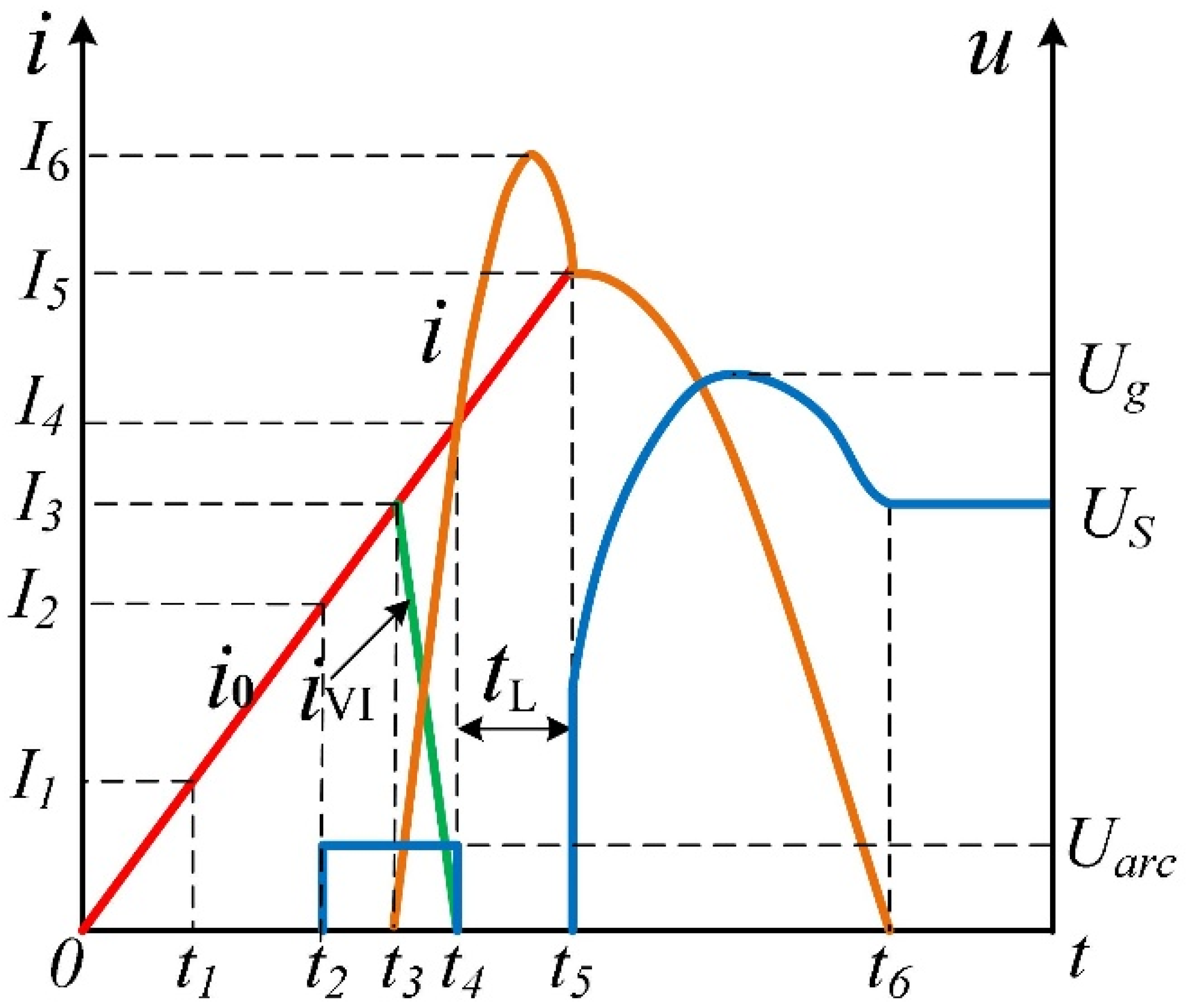
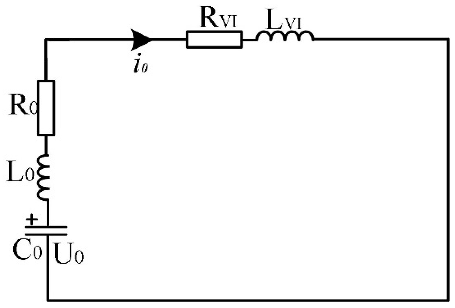
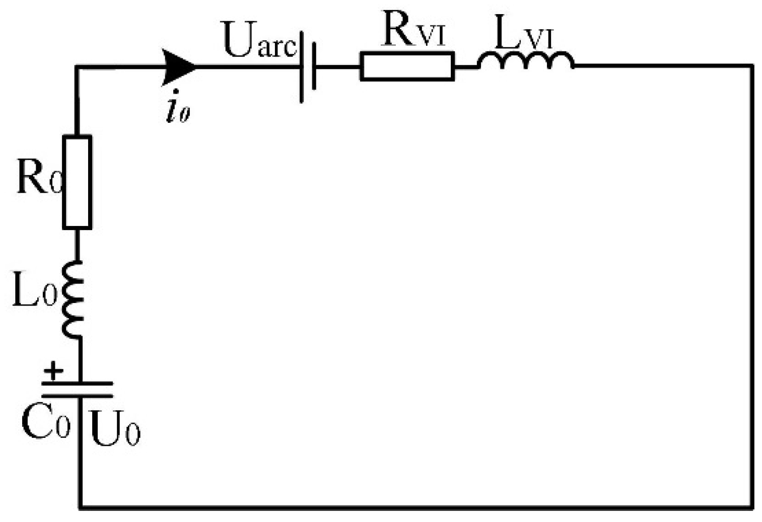
3. Equivalent Circuit and Preliminary Parameter Design in the Commutation Process
3.1. Equivalent Circuit in the Commutation Process
3.2. Preliminary Design of the Commutation Circuit Parameters
- (1)
- The peak value of the commutation circuit current I6 shall be greater than the corresponding main circuit current Imax;
- (2)
- In order to meet the need of dielectric recovery of the VI, zero-voltage time ;
- (3)
- The currents of the commutation circuit shall all flow through the VI to reduce the energy stored in the capacitor;
- (4)
- Due to the limitation of the short-time withstand of the thyristor, the initial rising rate of the current in the commutation circuit .
- (1)
- When , that is , L1 > L2
- (2)
- When , that is , L1 ≤ L2
- (1)
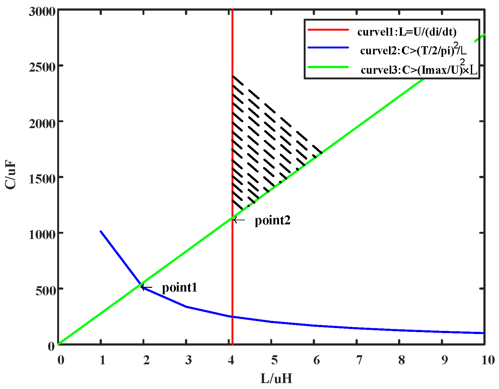
- When , the matching of optimization parameters is: current-limiting inductance and commutation capacitance . Each parameter is independent of the initial current rising rate of the commutation circuit and proportional to the zero-voltage time.
- (2)
- When , the matching of optimization parameters is: current-limiting inductance and commutation capacitance . Each parameter is independent of the zero-voltage time and inversely proportional to the initial current rising rate of the commutation circuit.
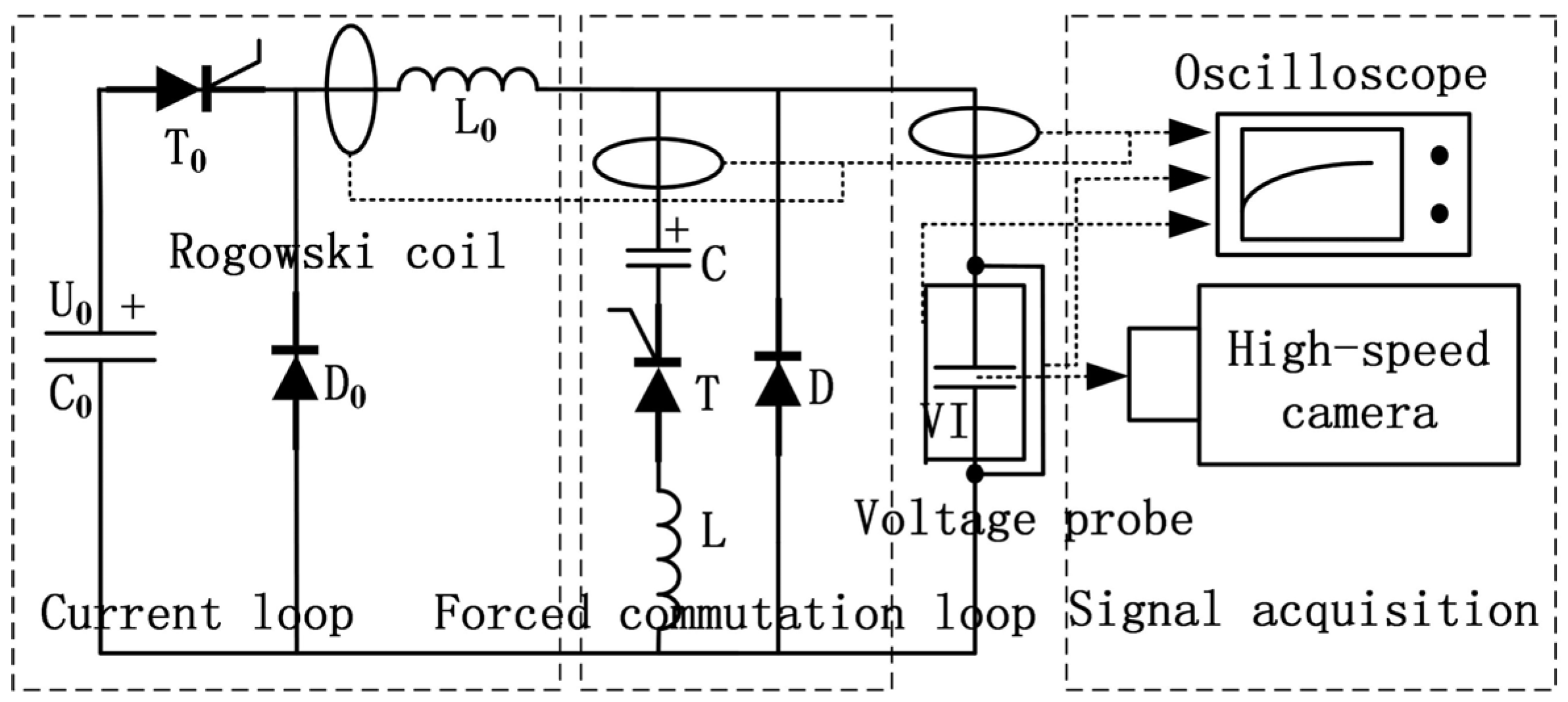
4. Circuit Simulation Model of the HDCCLCB
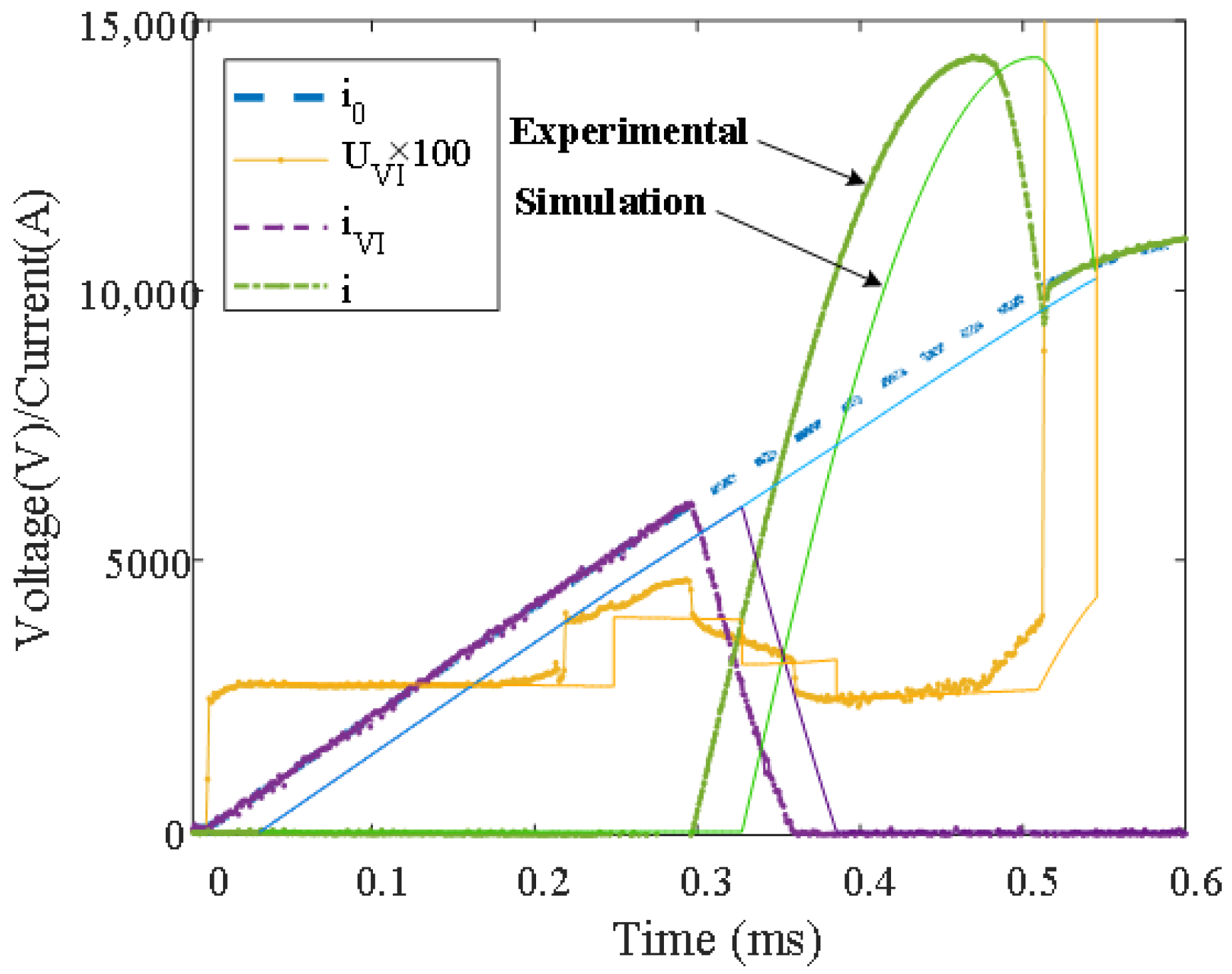
5. Prototype Experiment and Circuit Model Verification
6. Optimization Design of the Commutation Circuit Parameters
6.1. Optimization Analysis Model of the Commutation Circuit Parameters
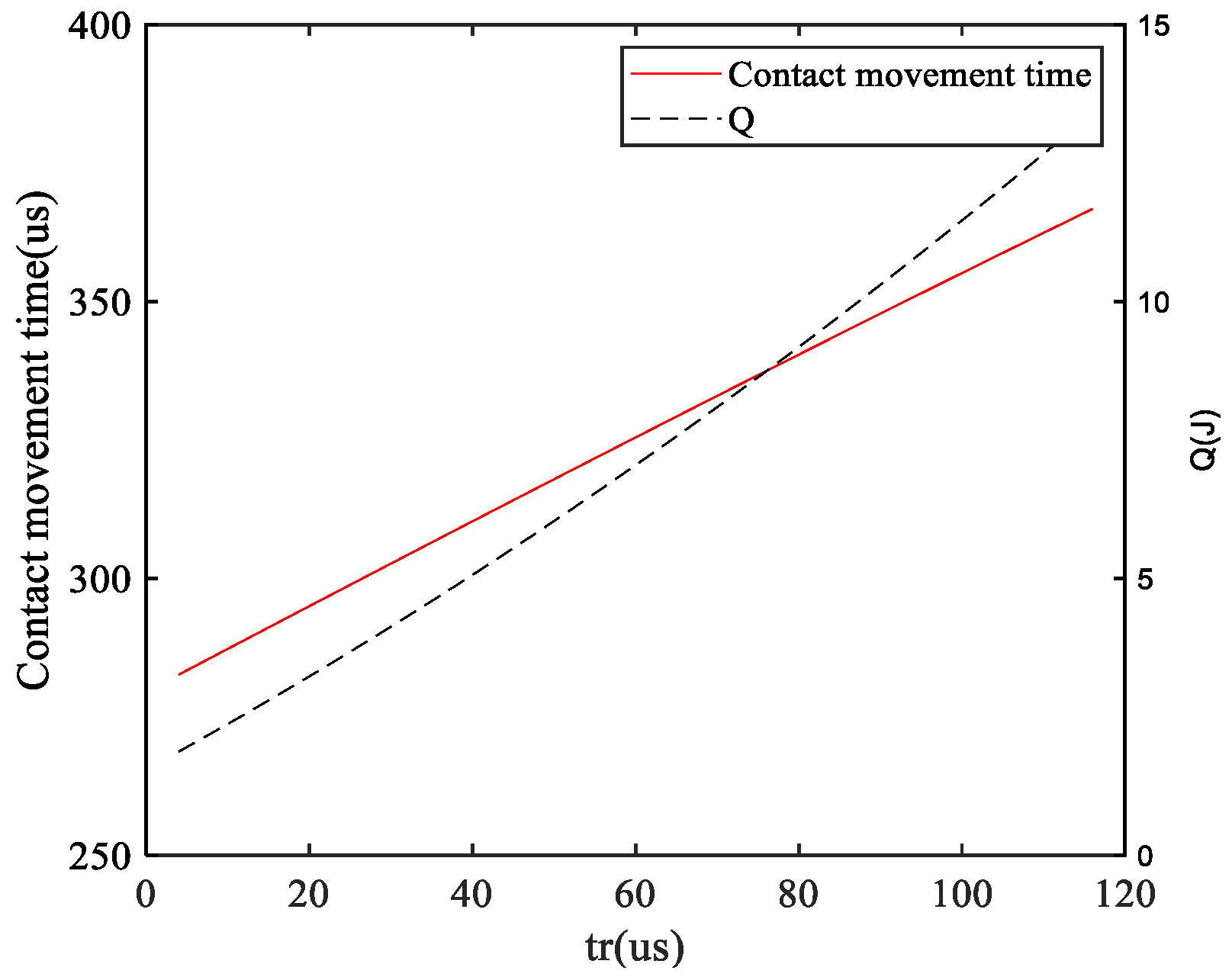
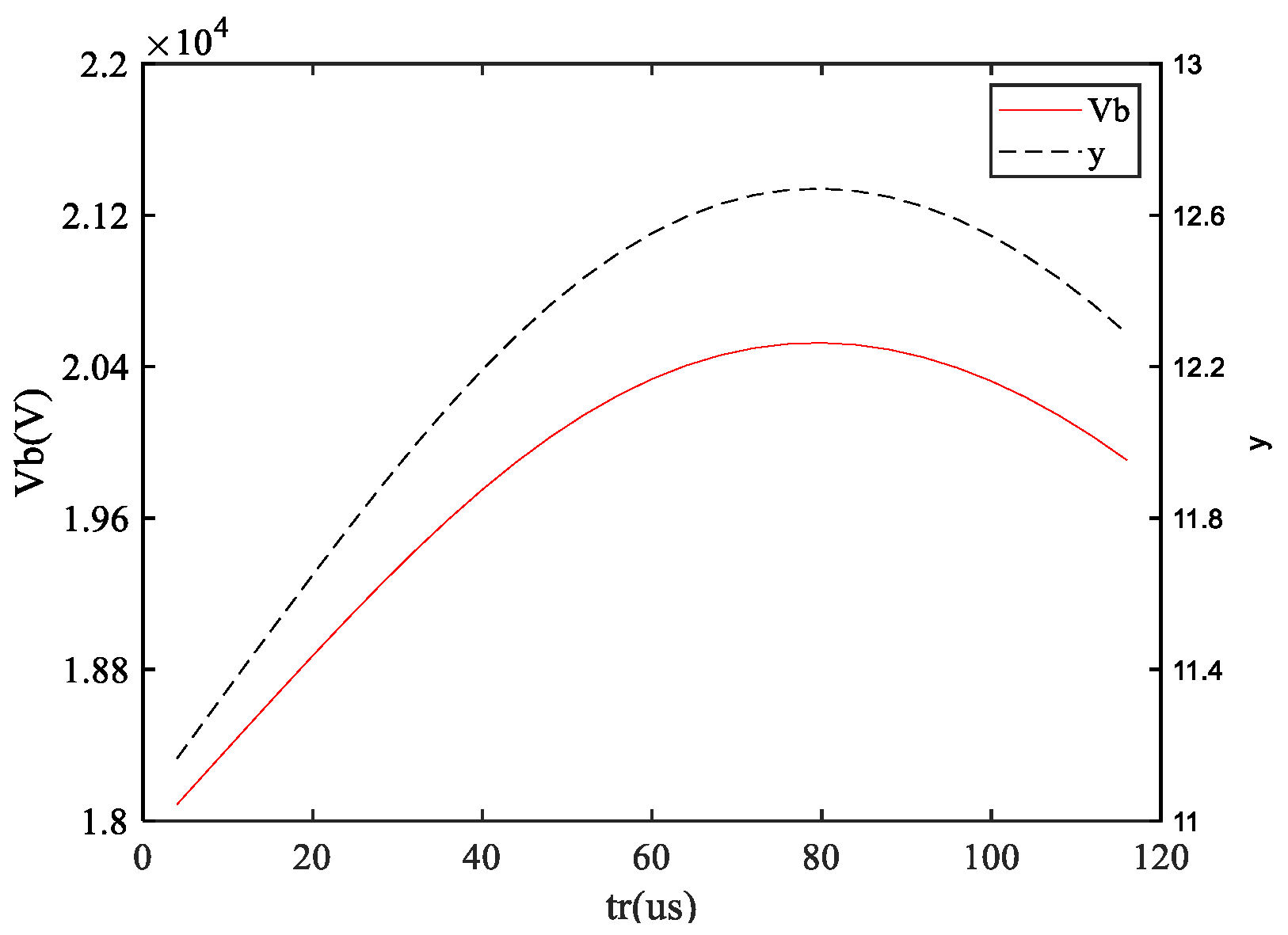
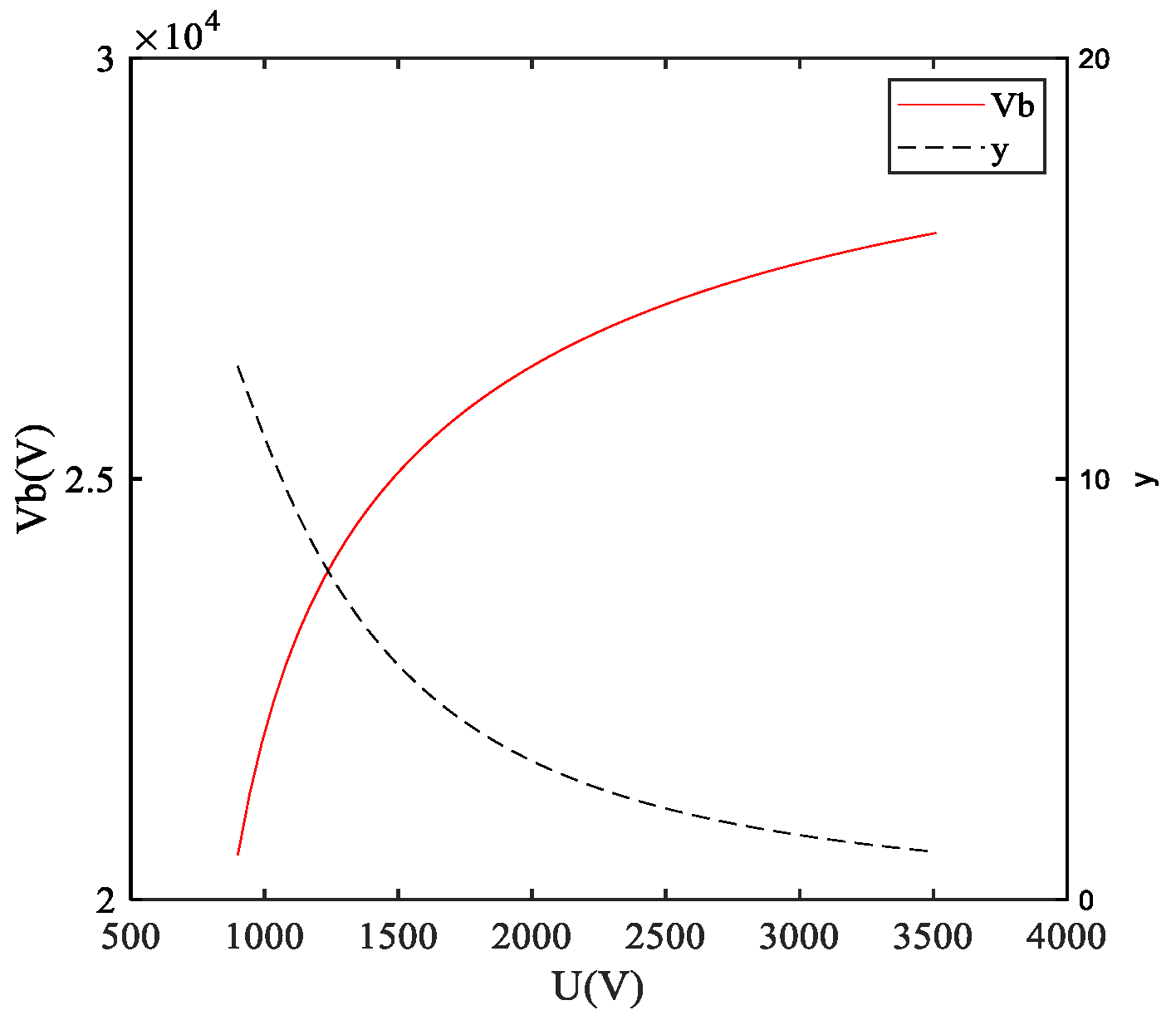
6.2. Influence of the Parameters on the Objective Function
6.3. Optimization Results and Simulation Comparison
7. Discussion
8. Conclusions
- (1)
- Under the condition of only changing the arcing time, with the increase in the arcing time, the critical breakdown voltage and the objective function of the contact firstly increase and then decrease, and there is a maximum value;
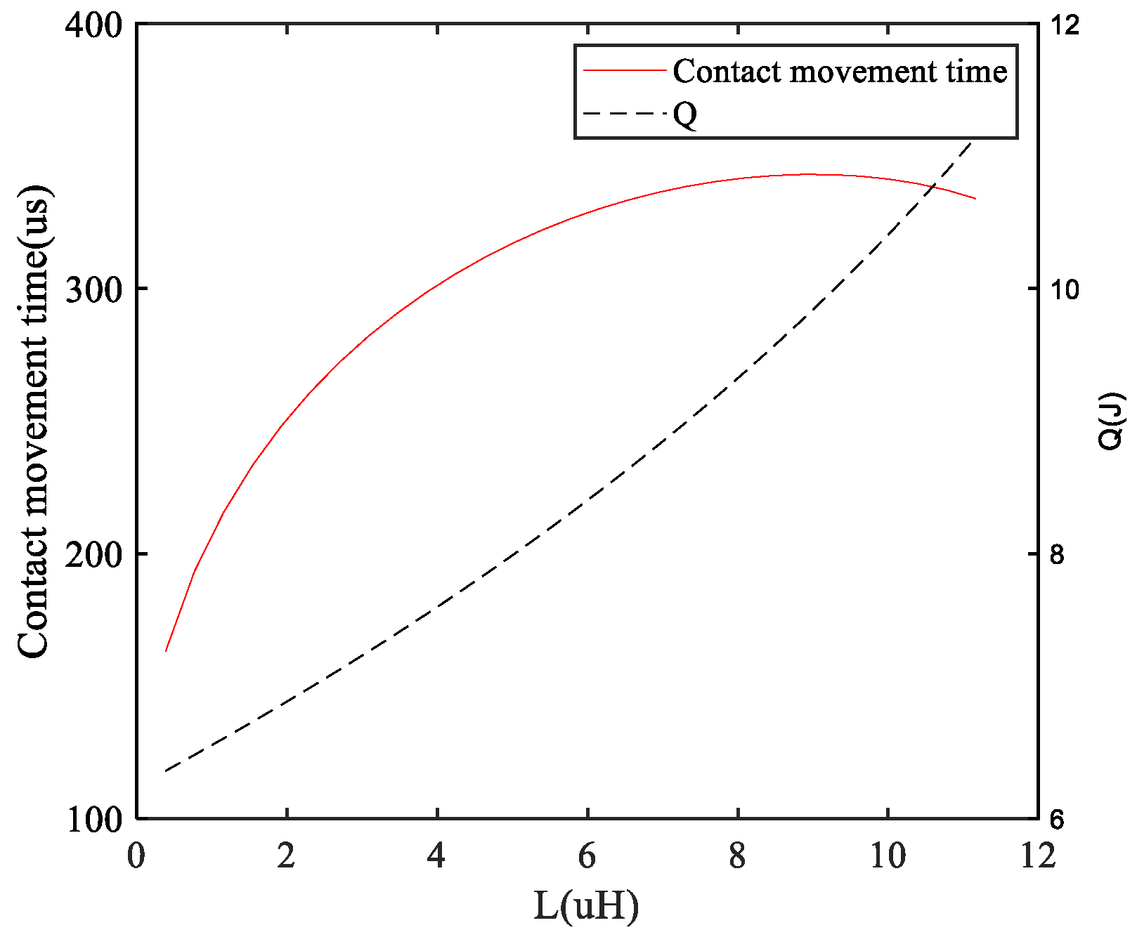
- (2)
- Under the condition of only changing the current-limiting inductance, with the increase in the current-limiting inductance, the critical breakdown voltage and the objective function of the contact firstly increase and then decrease, and there is a maximum value;
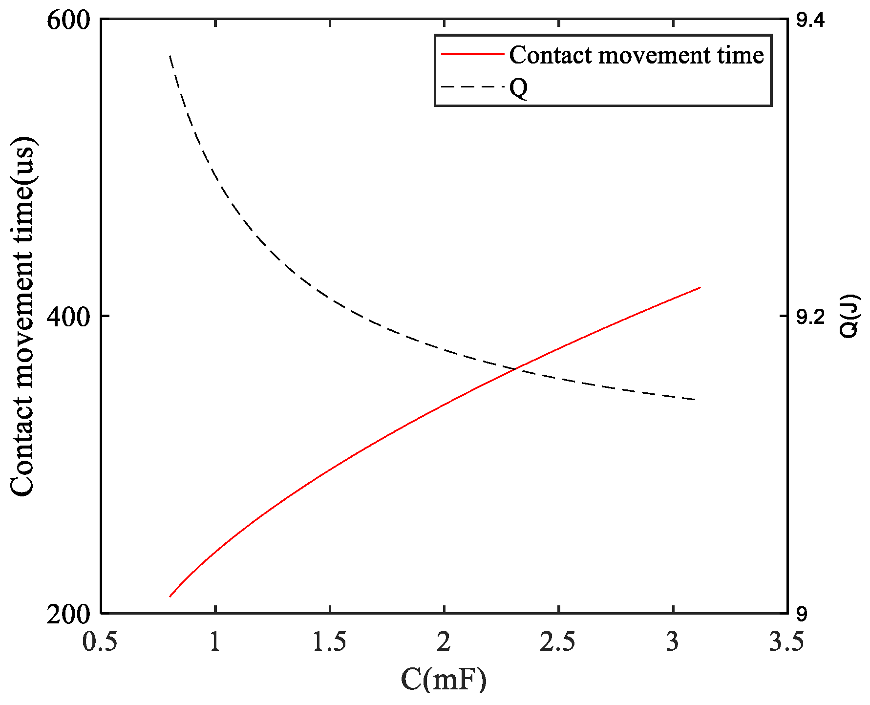
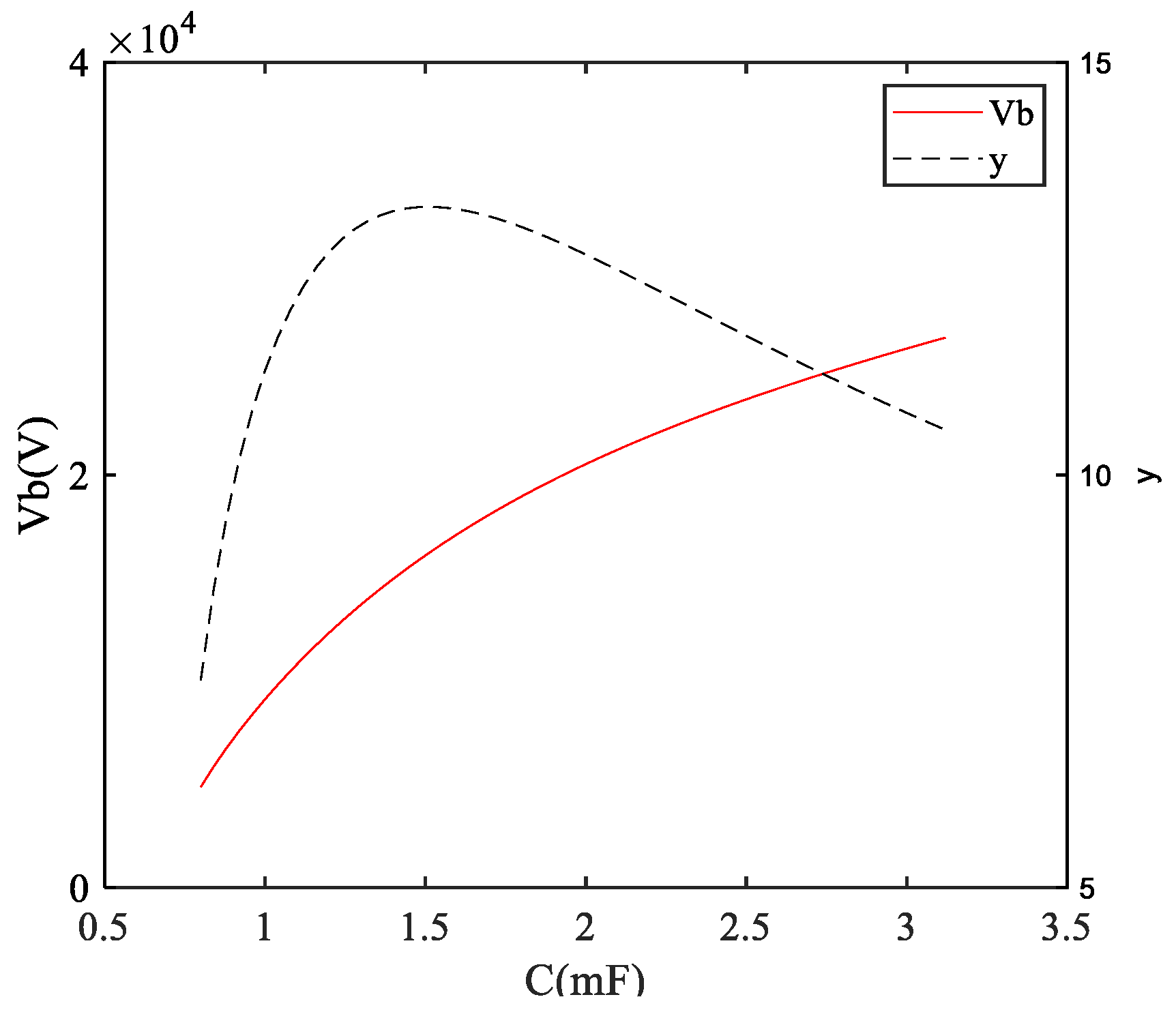
- (3)
- Under the condition of only changing the capacitance value, the critical breakdown voltage of the contact always increases with the increase in the capacitance value. The objective function firstly increases and then decreases, and there is a maximum value;
- (4)
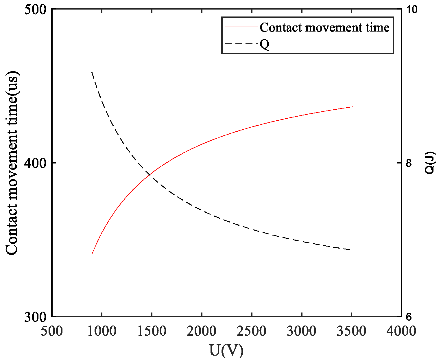
- Under the condition of only changing the capacitor voltage, the critical breakdown voltage of the contact increases with the increase in the capacitor voltage. The objective function always decreases;
- (5)
- By comprehensively considering the impact of various factors on the objective function rather than solely considering the impact of a single factor, further optimization of the objective function can be achieved;
- (6)
- The optimization design model established in this paper can optimize the parameters of the commutation circuit, laying a solid foundation for further analysis and the design of medium-voltage DC-current-limiting circuit breakers for ships.
Author Contributions
Funding
Data Availability Statement
Conflicts of Interest
References
- Zohrabi, N.; Shi, J.; Abdelwahed, S. An overview of design specifications and requirements for the MVDC shipboard power system. Int. J. Electr. Power Energy Syst. 2019, 104, 680–693. [Google Scholar] [CrossRef]
- Satpathi, K.; Ukil, A.; Pou, J. Short-circuit fault management in DC electric ship propulsion system: Protection requirements, review of existing technologies and future research trends. IEEE Trans. Transp. Electrif. 2018, 4, 272–291. [Google Scholar] [CrossRef]
- Fu, L.; Liu, L.; Wang, G.; Ma, F.; Ye, Z.; Ji, F.; Liu, L. The research progress of the medium voltage DC integrated power system in China. Chin. J. Ship Res. 2016, 11, 72–79. (In Chinese) [Google Scholar]
- Desbaillet, M. DC High Speed Circuit Breaker UR6 Instructions Manual Document Number: HSBA601103TEN; Secheron SA: Geneva, Switzerland, 2008. [Google Scholar]
- Xu, Z.; Zhang, B.; Sirisukprasert, S.; Zhou, X.; Huang, A.Q. The emitter turn-off thyristor based DC circuit breaker. In Proceedings of the 2002 IEEE Power Engineering Society Winter Meeting, New York, NY, USA, 27–31 January 2002; Volume 1, pp. 288–293. [Google Scholar]
- Agostini, F.; Vemulapati, U.; Torresin, D.; Arnold, M.; Rahimo, M.; Antoniazzi, A.; Raciti, L.; Pessina, D.; Suryanarayana, H. 1MW bi-directional DC solid state circuit breaker based on air cooled re-verse blocking IGCT. In Proceedings of the 2015 IEEE Electric Ship Technologies Symposium (ESTS), Alexandria, VA, USA, 21–24 June 2015; IEEE: Piscataway, NJ, USA, 2015; pp. 287–292. [Google Scholar]
- Kempkes, M.; Roth, I.; Gaudreau, M. Solid-state circuit breakers for medium voltage DC power. In Proceedings of the 2011 IEEE Electric Ship Technologies Symposium, Alexandria, VA, USA, 10–13 April 2011; IEEE: Piscataway, NJ, USA, 2011; pp. 254–257. [Google Scholar]
- Shukla, A.; Demetriades, G.D. A survey on hybrid circuit breaker topologies. IEEE Trans. Power Deliv. 2015, 30, 627–641. [Google Scholar] [CrossRef]
- Polman, H.; Ferreira, J.A.; Kaanders, M.; Evenblij, B.H.; Van Gelder, P. Design of a bi-directional 600V/6kA ZVS hybrid DC switch using IGBTs. IEEE Trans. Power Deliv. 2001, 16, 1052–1059. [Google Scholar]
- Meyer, J.; Rufer, A. A DC hybrid circuit breaker with ultra-fast contact opening and integrated gate-commutated thyristors (IGCTs). IEEE Trans. Power Deliv. 2006, 21, 646–651. [Google Scholar] [CrossRef]
- Häfner, J.; Jacobson, B. Proactive hybrid HVDC breakers—A key innovation for reliable HVDC grids. In Proceedings of the International Symposium on Integrating Supergrids and Microgrids, Bologna, Italy, 13–15 September 2011; CIGRE: Paris, France, 2011; pp. 1–8. [Google Scholar]
- Grieshaber, W.; Violleau, L. Development and Test of a 120 kV Direct Current Circuit Breaker; CIGRE Session; CIGRE: Paris, France, 2014; pp. 1–11. [Google Scholar]
- Greenwood, A.N.; Lee, T.H. Theory and application of the com-mutation principle for HVDC circuit breakers. IEEE Trans-Actions Power Appar. Syst. 1972, 91, 1570–1574. [Google Scholar] [CrossRef]
- Anderson, J.; Carroll, J. Applicability of a vacuum interrupter as the basic switch element in HVDC breakers. IEEE Trans. Power Appar. Syst. 1978, 97, 1893–1900. [Google Scholar] [CrossRef]
- Premerlani, W. Forced commutation performance of vacuum switches for HVDC breaker ap-plication. IEEE Trans. Power Appar. Syst. 1982, 101, 2721–2727. [Google Scholar] [CrossRef]
- Roberto, P.; Loris, Z.; Bonicelli, T. Vacuum breaker for high DC current: Experimental performances and operational limits. IEEE Trans. Plasma Sci. 2009, 37, 229–235. [Google Scholar]
- Niwa, Y.; Yokokura, K.; Matsuzaki, J. Fundamental investigation and application of high speed VCB for DC power system of railway. In Proceedings of the 24th International Symposium on Discharges and Electrical Insulation in Vacuum, Braunschweig, Germany, 30 August–3 September 2010; IEEE: Piscataway, NJ, USA, 2010; pp. 125–128. [Google Scholar]
- Niwa, Y.; Matsuzaki, J.; Yokokura, K. The basic investigation of the high-speed VCB and its application for the DC power system. In Proceedings of the 23rd International Symposium on Discharges and Electrical Insulation in Vacuum, Bucharest, Romania, 15–19 September 2008; IEEE: Piscataway, NJ, USA, 2008; pp. 107–112. [Google Scholar]
- Liu, L.; Zhuang, J.; Wang, C.; Jiang, Z.; Wu, J.; Chen, B. A hybrid DC vacuum circuit breaker for medium voltage: Principle and first measurements. IEEE Trans. Power Deliv. 2014, 30, 2096–2101. [Google Scholar] [CrossRef]
- Shi, Z.Q.; Jia, S.L.; Ma, M.; Song, X.C.; Yang, H.Y.; Liu, C.; Wang, L.J. Investigation on DC interruption based on artifcial current zero of vacuum switch. In Proceedings of the XXIVth International Symposium on Discharges and Electrical Insulation in Vacuum, Braunschweig, Germany, 30 August–3 September 2010; IEEE: Piscataway, NJ, USA, 2010; pp. 158–161. [Google Scholar]
- Rachi, M.R.K.; Husain, I. Metal Oxide Varistor Design Optimization and Main Breaker Branch Switch Control of a Progressively Switched Hybrid DC Circuit Breaker. IEEE Trans. Ind. Appl. 2022, 58, 3064–3075. [Google Scholar] [CrossRef]
- Kaisar Rachi, M.R.; Husain, I. Main Breaker Switching Control and Design Optimization for A Progressively Switched Hybrid DC Circuit Breaker. In Proceedings of the 2020 IEEE Energy Conversion Congress and Exposition (ECCE), Detroit, MI, USA, 11–15 October 2020; pp. 6016–6023. [Google Scholar]
- Jehle, A.; Biela, J. Optimization of Hybrid Current-Injection Circuit Breakers Including Mechanical Switch Limitations. In Proceedings of the 2019 21st European Conference on Power Electronics and Applications (EPE ‘19 ECCE Europe), Genova, Italy, 3–5 September 2019; pp. P.1–P.11. [Google Scholar]
- Yu, D.; Chen, H.; Liu, W.; Liu, X. Optimization of commutation circuit parameters for DC vacuum circuit breakers. J. Eng. 2019, 2019, 2585–2588. [Google Scholar] [CrossRef]
- Liu, X.; Yu, D.; Zou, J.; Liao, M. Multi-objective optimization design of commutation circuit in DC vacuum circuit breaker. In Proceedings of the 2014 International Symposium on Discharges and Electrical Insulation in Vacuum (ISDEIV), Mumbai, India, 28 September–3 October 2014; IEEE: Piscataway, NJ, USA, 2014; pp. 141–144. [Google Scholar]
- Darwish; Izzularab; Elkalashy. Enhanced commutation circuit design of HVDC circuit breaker using EMTP. In Proceedings of the 2005/2006 IEEE/PES Transmission and Distribution Conference and Exhibition, Dallas, TX, USA, 21–24 May 2006; IEEE: Piscataway, NJ, USA, 2006; pp. 978–985. [Google Scholar]
- Jiang, Z.X.; Zhuang, J.W.; Liu, L.H.; Wu, J.; Wang, C.; Wu, H.J. A new DC vacuum circuit breaker based on artificial current zero. J. Nav. Univ. Eng. 2012, 24, 20–25. (In Chinese) [Google Scholar]
- Jiang, Z.; Zhuang, J.; Wang, C.; Wu, J.; Liu, L. Vacuum dielectric recovery characteristics of a novel current limiting circuit breaker base on artificial current zero. Proc. CSEE 2012, 32, 152–158. (In Chinese) [Google Scholar]
- Jiang, Z.X.; Zhuang, J.W.; Wang, C.; Wu, J.; Liu, L.H. Analysis and design of a bidirectional non-uniform vacuum DC hybrid circuit breaker. Proc. CSEE 2013, 33, 142–147. (In Chinese) [Google Scholar]


| Time | Event |
|---|---|
| 0 μs | Short circuit fault occurs |
| 100 μs | Fault detection time |
| 220 μs | Inherent time of the vacuum interrupter |
| 290 μs | Arcing time before commutating |
| tr/μs | L/μH | C/mF | U/V | |
|---|---|---|---|---|
| 1 | 24 | 7.5 | 2 | 900 |
| 2 | 24 | 6.16 | 1.2 | 900 |
| Parameter | Preliminary Design | Optimization Design | Percentage Difference |
|---|---|---|---|
| di/dt/(A/μs) | 120 | 146 | +21.7% |
| Q/J | 3.52 | 3.14 | −10.8% |
| CU2/J | 1620 | 972 | −40% |
| Vb/V | 18,955 | 13,733 | −27.5% |
| y | 11.70 | 14.12 | +20.7% |
| No Limitations on di/dt and tL | Only Considering the Limitation on tL | Only Considering the Limitation on di/dt | Considering the Limitations on di/dt and tL | |
|---|---|---|---|---|
| tL/μs | 19.45 | 152 > 150 | 17.76 | 156 > 150 |
| di/dt/(A/μs) | 360 | 240 | 180 < 220 | 120 < 220 |
| L/μH | 1.875 | 1.875 | 3.75 | 3.75 |
| C/mF | 0.5 | 4 | 1 | 4 |
| U/V | 675 | 450 | 675 | 450 |
| tr/μs | 160 | 140 | 140 | 60 |
| Q/J | 19.37 | 17.43 | 18.69 | 9.54 |
| CU2/J | 228 | 810 | 456 | 810 |
| Vb/V | 12,900 | 20,100 | 14,100 | 17,900 |
| y | 56.58 | 24.81 | 30.92 | 22.10 |
Disclaimer/Publisher’s Note: The statements, opinions and data contained in all publications are solely those of the individual author(s) and contributor(s) and not of MDPI and/or the editor(s). MDPI and/or the editor(s) disclaim responsibility for any injury to people or property resulting from any ideas, methods, instructions or products referred to in the content. |
© 2023 by the authors. Licensee MDPI, Basel, Switzerland. This article is an open access article distributed under the terms and conditions of the Creative Commons Attribution (CC BY) license (https://creativecommons.org/licenses/by/4.0/).
Share and Cite
Lv, Z.; Zhuang, J.; Wu, J.; Liu, L.; Yuan, Z.; Jiang, Z.; Wang, X. Parameter Optimization Design of the Commutation Circuit of a Hybrid DC-Current-Limiting Circuit Breaker. Energies 2023, 16, 7546. https://doi.org/10.3390/en16227546
Lv Z, Zhuang J, Wu J, Liu L, Yuan Z, Jiang Z, Wang X. Parameter Optimization Design of the Commutation Circuit of a Hybrid DC-Current-Limiting Circuit Breaker. Energies. 2023; 16(22):7546. https://doi.org/10.3390/en16227546
Chicago/Turabian StyleLv, Zhiyong, Jinwu Zhuang, Jin Wu, Luhui Liu, Zhifang Yuan, Zhuangxian Jiang, and Xiangjun Wang. 2023. "Parameter Optimization Design of the Commutation Circuit of a Hybrid DC-Current-Limiting Circuit Breaker" Energies 16, no. 22: 7546. https://doi.org/10.3390/en16227546