
Band-to-Band Transitions in InAs/GaSb Multi-Quantum-Well Structures Using k.p Theory: Effects of Well/Barrier Width and Temperature
 , , , , ,
Abstract
:
1. Introduction
2. Theory
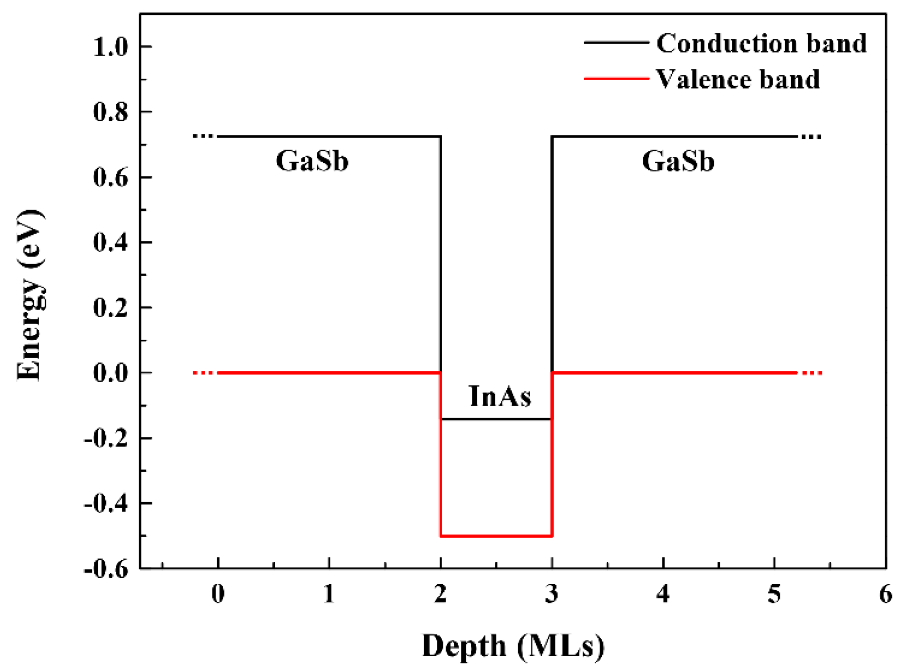
2.1. The k.p Hamiltonian
2.2. Discretization with FDM
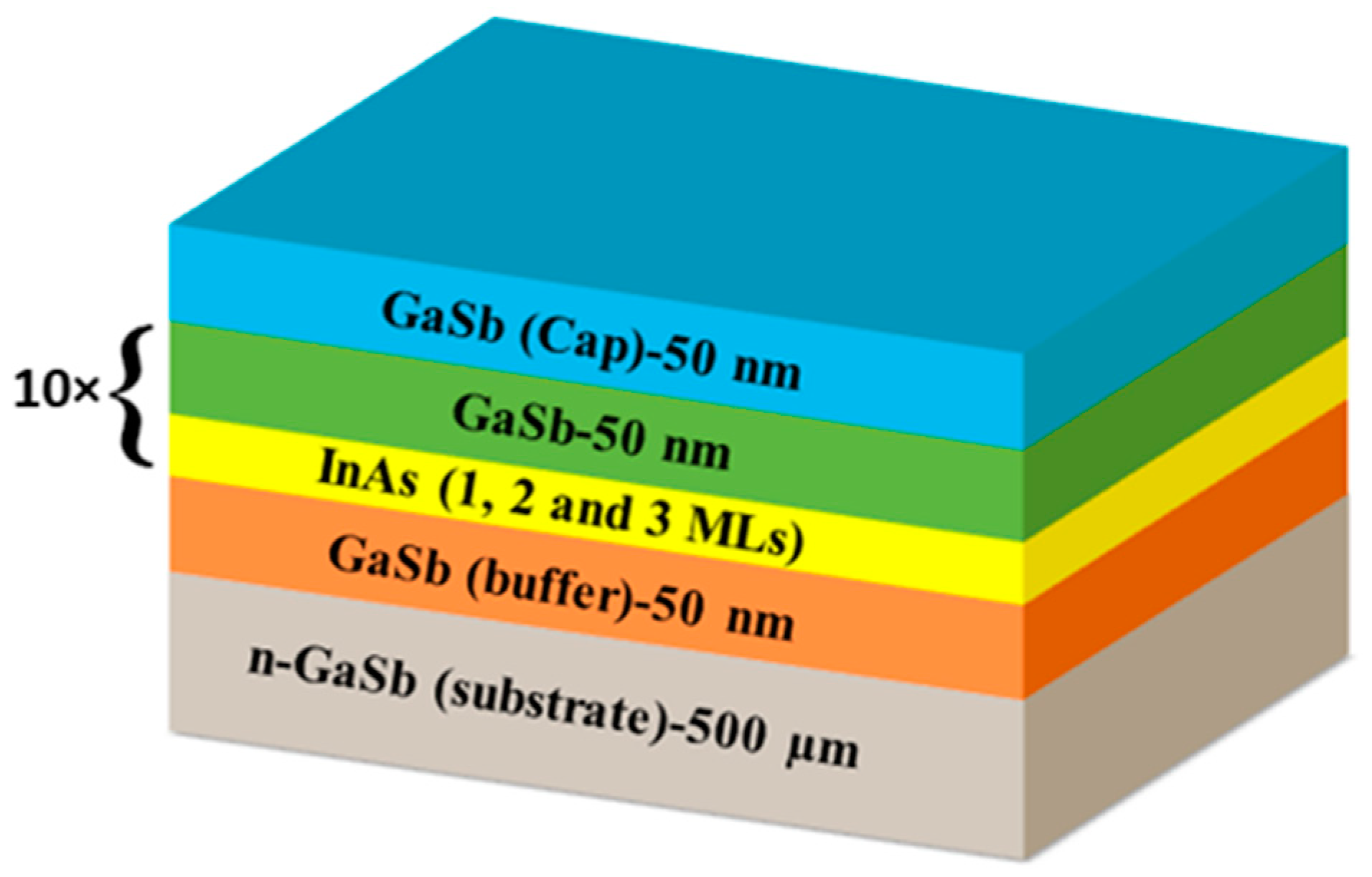
3. Experimental Section
4. Results and Discussion
4.1. Numerical Simulation
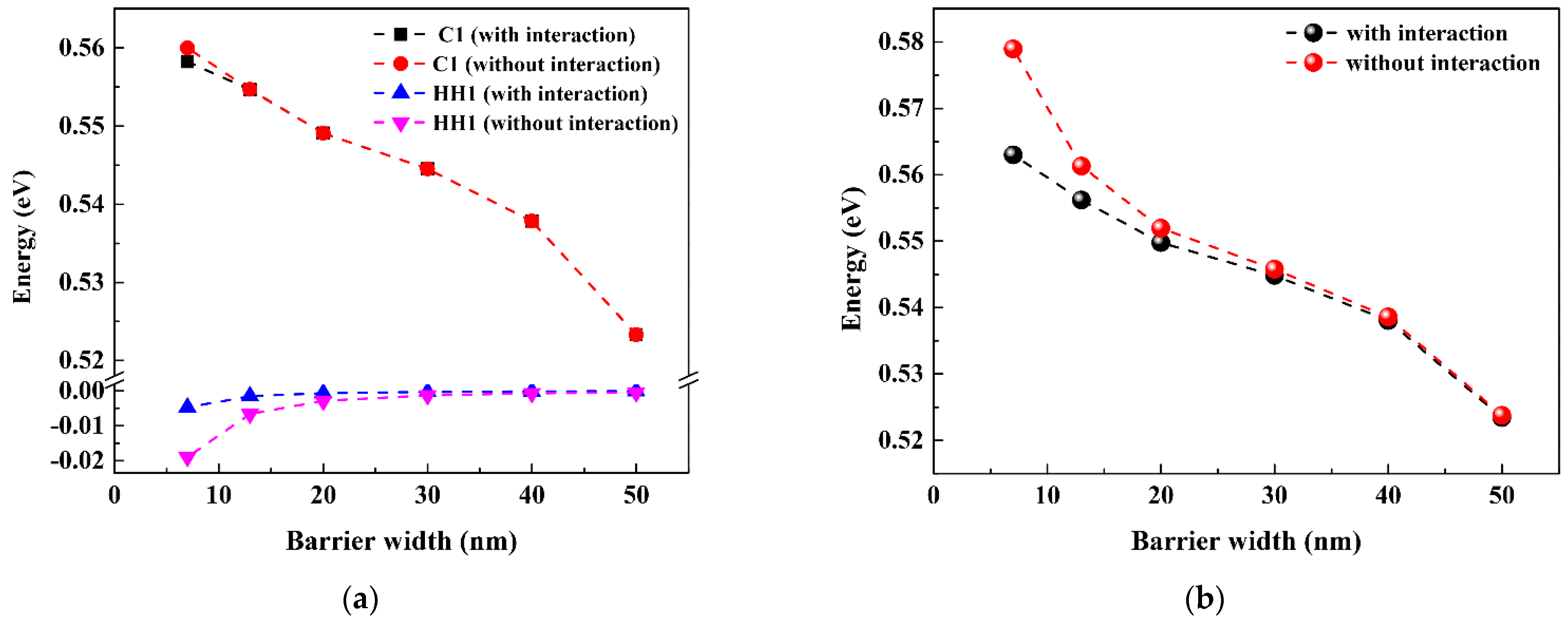
4.1.1. Effect of the Barrier Width on the Well’s Interactions
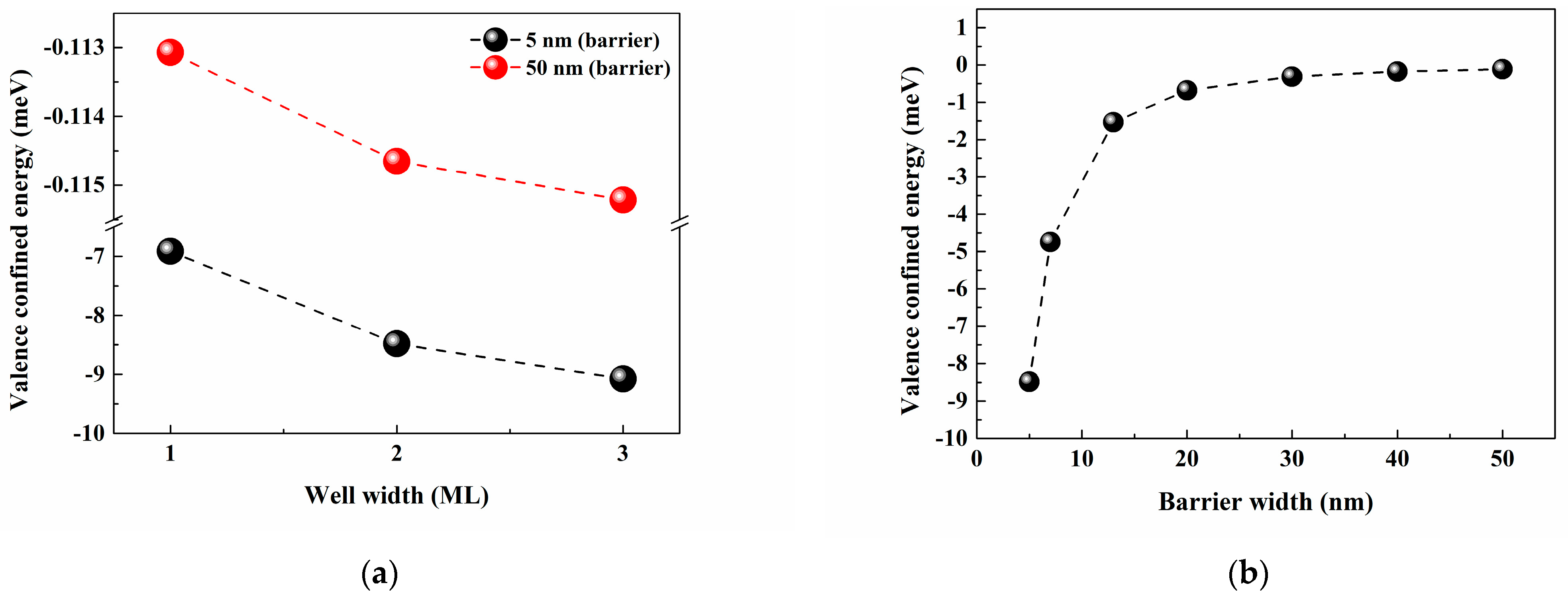
4.1.2. Effect of Barrier Widths on Valence-Band Energy Levels
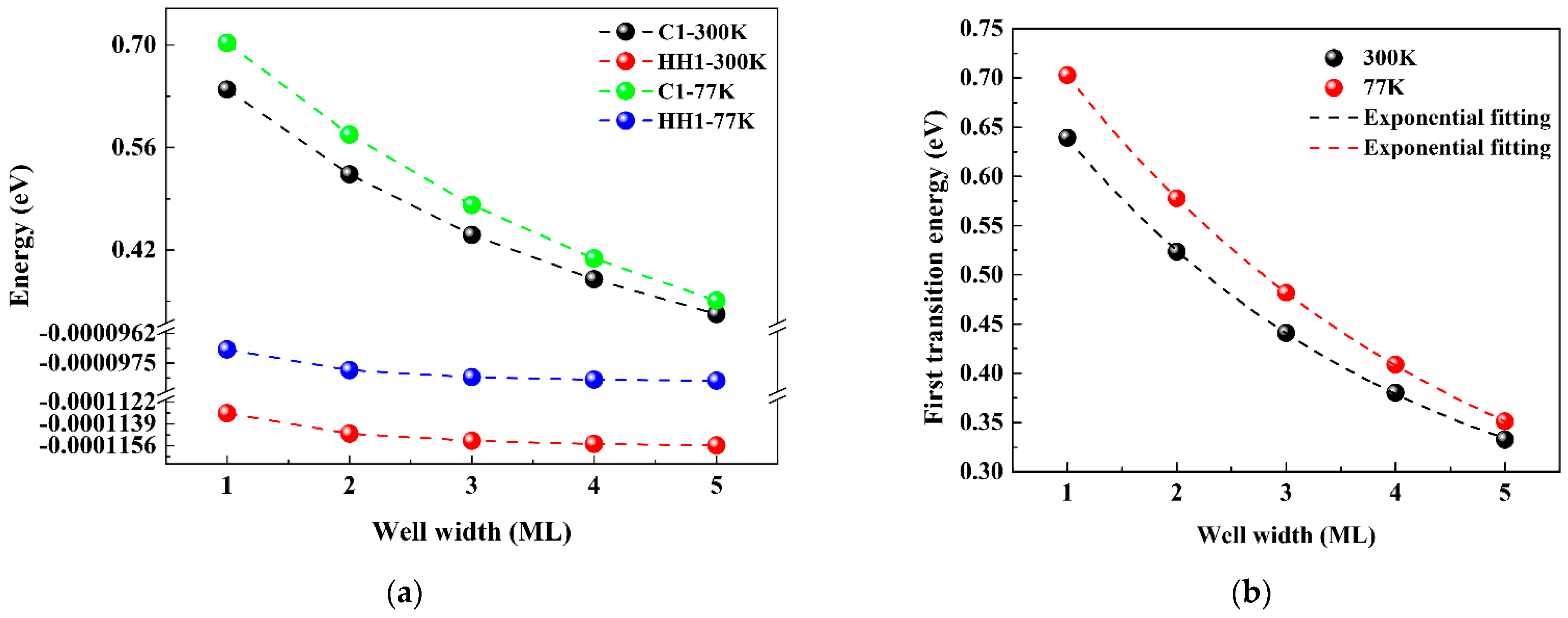
4.1.3. Transition Energies for Different Well Widths and Temperatures
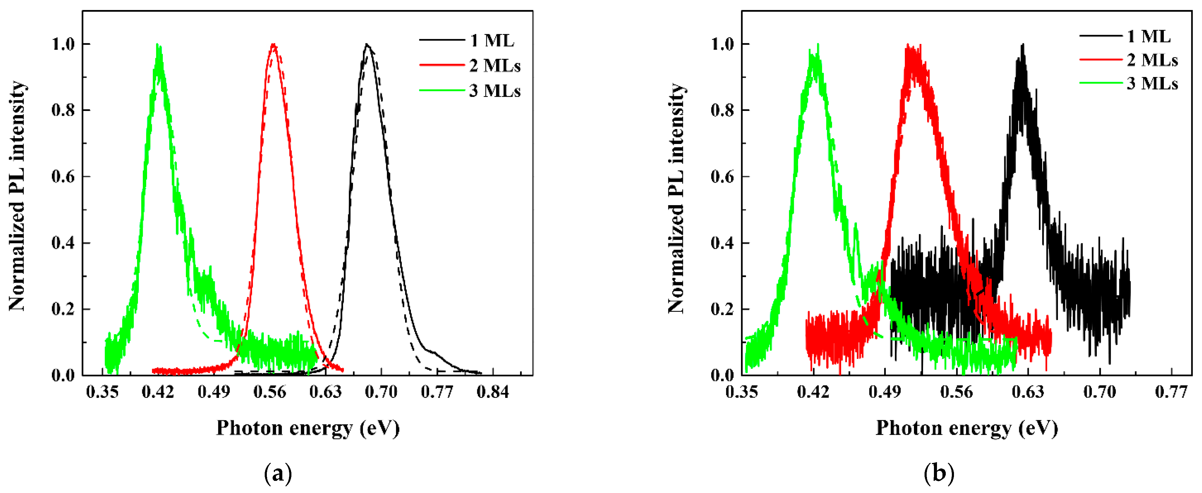
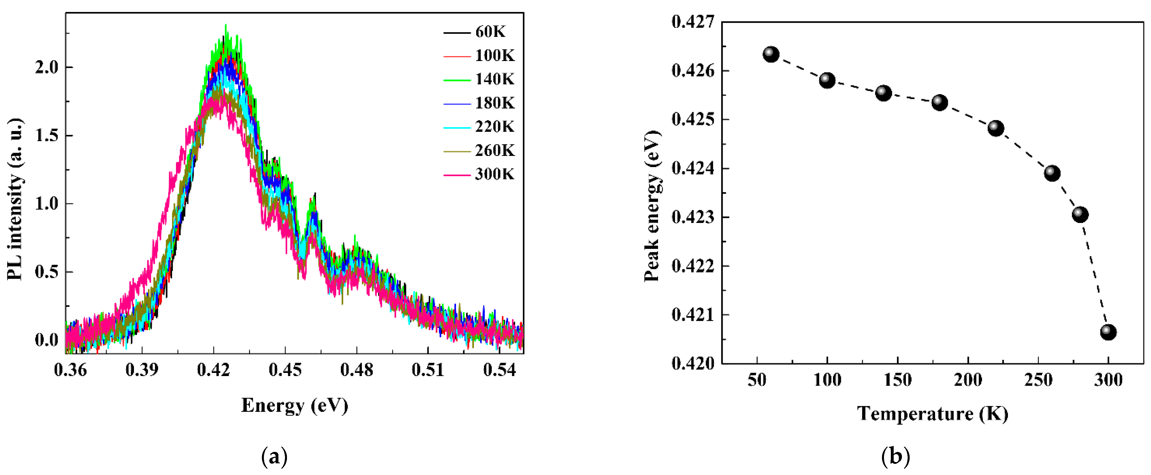
4.2. Experimental Results
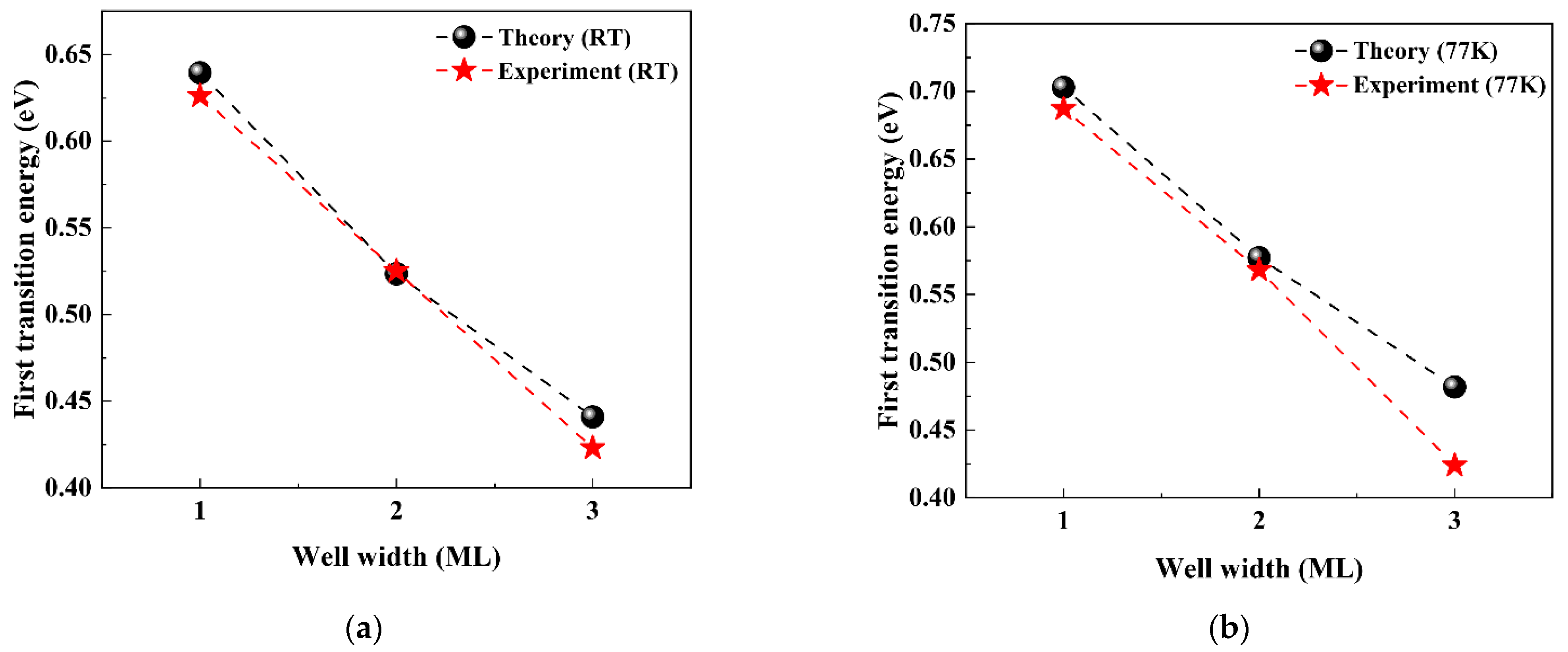
4.3. Comparisons of Theoretical and Experimental Results
5. Conclusions
Author Contributions
Funding
Institutional Review Board Statement
Informed Consent Statement
Data Availability Statement
Conflicts of Interest
Appendix A
References
- Bennett, B.; Soref, R. Electrorefraction and electroabsorption in InP, GaAs, GaSb, InAs, and InSb. IEEE J. Quantum Electron. 1987, 23, 2159–2166. [Google Scholar] [CrossRef]
- Mahajumi, A.S. InAs/GaSb Quantum Well Structures of Infrared Detector Applications: Quantum Well Structure. Master’s Thesis, Halmstad University, Halmstad, Sweden, 2010. [Google Scholar]
- Halvorsen, E.; Galperin, Y.; Chao, K.A. Optical transitions in broken gap heterostructures. Phys. Rev. B 2000, 61, 16743. [Google Scholar] [CrossRef] [Green Version]
- Xu, W.; Li, L.L.; Dong, H.M.; Gumbs, G.; Folkes, P.A. Band hybridization and spin-splitting in InAs/AlSb/GaSb type II and broken-gap quantum wells. J. Appl. Phys. 2010, 108, 053709. [Google Scholar] [CrossRef] [Green Version]
- Schulman, J.N.; Chang, Y.C. New method for calculating electronic properties of superlattices using complex band structures. Phys. Rev. B 1981, 24, 4445. [Google Scholar] [CrossRef]
- Chang, Y.C.; Schulman, J.N. Theory of heterostructures: A reduced hamiltonian method with evanescent states and transfer matrices. J. Vac. Sci. Technol. 1982, 21, 540–543. [Google Scholar] [CrossRef]
- Schuurmans, M.F.H. Simple calculations of confinement states in a quantum well. Phys. Rev. B 1985, 31, 8041. [Google Scholar] [CrossRef]
- Debbichi, M.; Ben Fredj, A.; Said, M.; Lazzari, J.L.; Cuminal, Y.; Christol, P. Nitrogen effect on optical gain and radiative current density for mid-infrared InAs (N)/GaSb/InAs (N) quantum-well laser. Phys. E Low-Dimens. Syst. Nanostruct. 2008, 40, 489–493. [Google Scholar] [CrossRef]
- Boutramine, A.; Nafidi, A.; Barkissy, D.; Hannour, A.; Elanique, A.; El Gouti, T. Application of the transition semiconductor to semimetal in type II nanostructure superlattice for mid-infrared optoelectronic devices. Appl. Phys. A 2016, 122, 330. [Google Scholar] [CrossRef]
- Ohtani, K.; Ohno, H. Mid-infrared intersubband electroluminescence in InAs/GaSb/AlSb type-II cascade structures. Phys. E Low-Dimens. Syst. Nanostruct. 2000, 7, 80–83. [Google Scholar] [CrossRef]
- Razeghi, M. High-power laser diodes based on InGaAsP alloys. Nature 1994, 369, 631–633. [Google Scholar] [CrossRef]
- Dan, F.; Chenglin, L.; Jiaxu, G.; Xuan, F.; Jilong, T. Type II InAs/GaSb superlattice growth via molecular beam epitaxy. Optik 2019, 198, 163208. [Google Scholar] [CrossRef]
- Gassenq, A.; Boissier, G.; Grech, P.; Narcy, G.; Baranov, A.; Tournié, E. InAs/GaSb/InSb short-period super-lattice diode lasers emitting near 3.3 µm at room-temperature. Electron. Lett. 2009, 45, 165–167. [Google Scholar] [CrossRef]
- Hong, B.H.; Rybchenko, S.I.; Itskevich, I.E.; Haywood, S.K.; Intartaglia, R.; Tasco, V.; Raino, G.; de Giorgi, M. Applicability of the k.p method to modeling of InAs/GaSb short-period superlattices. Phys. Rev. B 2009, 79, 165323. [Google Scholar] [CrossRef] [Green Version]
- Koerperick, E.J.; Olesberg, J.T.; Hicks, J.L.; Prineas, J.P.; Boggess, T.F. Active region cascading for improved performance in InAs–GaSb superlattice LEDs. IEEE J. Quantum Electron. 2008, 44, 1242–1247. [Google Scholar] [CrossRef]
- Deguffroy, N.; Tasco, V.; Gassenq, A.; Cerutti, L.; Trampert, A.; Baranov, A.N.; Tournié, E. InAs/GaSb short-period superlattice injection lasers operating in 2.5 µm–3.5 µm mid-infrared wavelength range. Electron. Lett. 2007, 43, 1285–1286. [Google Scholar] [CrossRef]
- Ridene, S.; Debbichi, M.; ben Fredj, A.; Said, M.; Bouchriha, H. Energy-band structure and optical gain in strained InAs(N)/GaSb/InAs(N) quantum well lasers. J. Appl. Phys. 2008, 104, 063706. [Google Scholar] [CrossRef]
- Becer, Z.; Bennecer, A.; Sengouga, N. Modeling energy bands in type ii superlattices. Crystals 2019, 9, 629. [Google Scholar] [CrossRef] [Green Version]
- Rygała, M.; Ryczko, K.; Smołka, T.; Kujawa, D.; Martyniuk, P.; Ronningen, T.J.; Krishna, S.; Motyka, M. Investigating the physics of higher-order optical transitions in InAs/GaSb superlattices. Phys. Rev. B 2021, 104, 085410. [Google Scholar] [CrossRef]
- Chen, X.; Zhu, L.; Zhang, Y.; Zhang, F.; Wang, S.; Shao, J. Modulated Photoluminescence Mapping of Long-Wavelength Infrared in As/Ga Sb Type-II Superlattice: In-Plane Optoelectronic Uniformity. Phys. Rev. Appl. 2021, 15, 044007. [Google Scholar] [CrossRef]
- Alyamani, S.; Jo, H.J.; So, M.G.; Kim, J.S.; Hyeon, K.T.; Shin, J.C.; Kim, J.O. Optical Properties of InAs/GaSb Multiple Quantum Wells Grown by Molecule Beam Epitaxy. In Proceedings of the 54th Winter Annual Conference of The Korean Vacuum Society, Dunnae-myeon, Republic of Korea, 7–9 February 2018; p. 344. [Google Scholar]
- Hartree, D.R. The Wave Mechanics of an Atom with a Non-Coulomb Central Field. Part I. Theory and Methods. In Mathematical Proceedings of the Cambridge Philosophical Society; Cambridge University Press: Cambridge, UK, 1928; pp. 89–110. [Google Scholar]
- Wei, Y.; Razeghi, M. Modeling of type-II InAs/GaSb superlattices using an empirical tight-binding method and interface engineering. Phys. Rev. B 2004, 69, 085316. [Google Scholar] [CrossRef]
- Wang, J.; Zhang, Y. Band-gap corrected density functional theory calculations for InAs/GaSb type II superlattices. J. Appl. Phys. 2014, 116, 214301. [Google Scholar] [CrossRef] [Green Version]
- Sun, W.F.; Li, M.C.; Zhao, L.C. First-principles study of interface relaxation effect on interface and electronic structures of InAs/GaSb superlattices with different interface types. Superlattices Microstruct. 2011, 49, 81–90. [Google Scholar] [CrossRef]
- Ryczko, K.; Sęk, G.; Misiewicz, J. Eight-band k.p modeling of InAs/InGaAsSb type-II W-design quantum well structures for interband cascade lasers emitting in a broad range of mid infrared. J. Appl. Phys. 2013, 114, 223519. [Google Scholar] [CrossRef]
- Akhavan, N.D.; Umana-Membreno, G.A.; Gu, R.; Asadnia, M.; Antoszewski, J.; Faraone, L. Superlattice barrier HgCdTe nBn infrared photodetectors: Validation of the effective mass approximation. IEEE Trans. Electron Devices 2016, 63, 4811–4818. [Google Scholar] [CrossRef] [Green Version]
- Jonsson, B.; Eng, S. Solving the Schrodinger equation in arbitrary quantum-well potential profiles using the transfer matrix method. IEEE J. Quantum Electron. 1990, 26, 2025–2035. [Google Scholar] [CrossRef] [Green Version]
- Paul, S.F.P.; Fouckhardt, H. An improved shooting approach for solving the time-independent Schrödinger equation for III/V QW structures. Phys. Lett. A 2001, 286, 199–204. [Google Scholar] [CrossRef]
- Hayata, K.; Koshiba, M.; Nakamura, K.; Shimizu, A. Eigenstate calculation of quantum well structures using finite elements. Electron. Lett. 1988, 24, 614–616. [Google Scholar] [CrossRef]
- Le, K.Q. Finite element analysis of quantum states in layered quantum semiconductor structures with band nonparabolicity effect. Microw. Opt. Technol. Lett. 2009, 51, 1–5. [Google Scholar] [CrossRef]
- Ajnef, N.; Jemmali, W.Q.; Habchi, M.M.; Rebey, A. Biaxial strain effects on the band structure and absorption coefficient of GaAs1-x-yNxBiy/GaAs MQWs calculated using kp method. Optik 2020, 223, 165484. [Google Scholar] [CrossRef]
- Lapushkin, I.; Zakharova, A.; Yen, S.T.; Chao, K.A. A self-consistent investigation of the semimetal–semiconductor transition in InAs/GaSb quantum wells under external electric fields. J. Phys. Condens. Matter 2004, 16, 4677. [Google Scholar] [CrossRef]
- Taalat, R.; Rodriguez, J.B.; Delmas, M.; Christol, P. Influence of the period thickness and composition on the electro-optical properties of type-II InAs/GaSb midwave infrared superlattice photodetectors. J. Phys. D Appl. Phys. 2013, 47, 015101. [Google Scholar] [CrossRef]
- Fang, S.; Hao, R.; Zhang, L.; Guo, J.; Liu, W. Simulation of the band structure of InAs/GaSb type II superlattices utilizing multiple energy band theories. Front. Phys. 2022, 250. [Google Scholar] [CrossRef]
- Hudait, M.K.; Clavel, M.; Goley, P.S.; Xie, Y.; Heremans, J.J.; Jiang, Y.; Jiang, Z.; Smirnov, D.; Sanders, G.D.; Stanton, C.J.; et al. Structural, morphological and magnetotransport properties of composite semiconducting and Structural, morphological and magnetotransport properties of composite semiconducting and semimetallic InAs/GaSb superlattice structure. Mater. Adv. 2020, 1, 1099–1112. [Google Scholar] [CrossRef]
- Szmulowicz, F.; Haugan, H.; Brown, G.J. Effect of interfaces and the spin-orbit band on the band gaps of InAs/GaSb superlattices beyond the standard envelope-function approximation. Phys. Rev. B 2004, 69, 155321. [Google Scholar] [CrossRef] [Green Version]
- Kane, E.O. Physics of III-V compounds. Semicond. Semimet. 1966, 1, 75. [Google Scholar]
- Bastard, G. Wave Mechanics Applied to Semiconductor Heterostructures; Halstead: New York, NY, USA, 1988. [Google Scholar]
- Novik, E.G.; Pfeuffer-Jeschke, A.; Jungwirth, T.; Latussek, V.; Becker, C.R.; Landwehr, G.; Molenkamp, L.W. Band structure of semimagnetic Hg1-yMnyTe quantum wells. Phys. Rev. B 2005, 72, 035321. [Google Scholar] [CrossRef] [Green Version]
- Skolasinski, R.J. Topology, Magnetism, and Spin-Orbit: A Band Structure Study of Semiconducting Nanodevices. Ph.D. Dissertation, Delft University of Technology, Delft, The Netherlands, 2018. [Google Scholar]
- Dresselhaus, G. Spin-orbit coupling effects in zinc blende structures. Phys. Rev. 1955, 100, 580. [Google Scholar] [CrossRef]
- Hellwege, K.H.; Madelung, O. Physics of Group IV Elements and III-V Compounds. In Landolt-Bornstein New Series, Group III; Springer: Berlin/Heidelberg, Germany, 1982; Volume 17. [Google Scholar]
- Madelung, O. Intrinsic Properties of Group IV Elements and III-V, II-VI and I-VII Compounds. In Landolt-Bornstein New Series, Group III; Springee: Berlin/Heidelberg, Germany, 1987; Volume 22. [Google Scholar]
- Lawaetz, P. Valence-band parameters in cubic semiconductors. Phys. Rev. B 1971, 4, 3460. [Google Scholar] [CrossRef]
- Klipstein, P.C. Operator ordering and interface-band mixing in the Kane-like Hamiltonian of lattice-matched semiconductor superlattices with abrupt interfaces. Phys. Rev. B 2010, 81, 235314. [Google Scholar] [CrossRef] [Green Version]
- Datta, S. Quantum Transport: Atom to Transistor; Cambridge University Press: Cambridge, UK, 2005. [Google Scholar]
- Marchewka, M. Finite-difference method applied for eight-band k.p model for Hg1-xCdxTe/HgTe quantum well. Int. J. Mod. Phys. B 2017, 31, 1750137. [Google Scholar] [CrossRef]
- D’Anterroches, C.; Gerard, J.M. Analysis of MBE growth and atomic exchange in thin highly strained In As layers. Microsc. Microanal. Microstruct. 1994, 5, 213–236. [Google Scholar] [CrossRef]
- Majaron, B.; Verkruysse, W.; Tanenbaum, B.S.; Milner, T.E.; Nelson, J.S. Spectral variation of the infrared absorption coefficient in pulsed photothermal profiling of biological samples. Phys. Med. Biol. 2002, 47, 1929. [Google Scholar] [CrossRef] [PubMed]
- Varshni, Y.P. Temperature dependence of the energy gap in semiconductors. Physica 1967, 34, 149–154. [Google Scholar] [CrossRef]

| 77 K | 300 K | |||
|---|---|---|---|---|
| Parameter | InAs | GaSb | InAs | GaSb |
| 6.0584 | 6.0954 | 6.0584 | 6.0954 | |
| 0.418 | 0.814 | 0.359 | 0.725 | |
| 0.38 | 0.76 | 0.38 | 0.76 | |
| 22.42 | 22.75 | 22.19 | 23.47 | |
| 0.022 | 0.042 | 0.019 | 0.037 | |
| 20 | 11.87 | 23.8 | 14.48 | |
| 9 | 4.61 | 10.7 | 5.67 | |
| 9.16 | 4.99 | 10.39 | 5.6 | |
| −0.59 | 0 | −0.501 | 0 | |
| Parameter | 77 K | 300 K |
|---|---|---|
| A | 0.703 | 0.586 |
| b | 3.81 | 3.247 |
| y0 | 0.161 | 0.207 |
Disclaimer/Publisher’s Note: The statements, opinions and data contained in all publications are solely those of the individual author(s) and contributor(s) and not of MDPI and/or the editor(s). MDPI and/or the editor(s) disclaim responsibility for any injury to people or property resulting from any ideas, methods, instructions or products referred to in the content. |
© 2023 by the authors. Licensee MDPI, Basel, Switzerland. This article is an open access article distributed under the terms and conditions of the Creative Commons Attribution (CC BY) license (https://creativecommons.org/licenses/by/4.0/).
Share and Cite
Seyedein Ardebili, S.B.; Kim, J.S.; Ha, J.; Kang, T.I.; Zeinalvand Farzin, B.; Kim, Y.; Lee, S.J. Band-to-Band Transitions in InAs/GaSb Multi-Quantum-Well Structures Using k.p Theory: Effects of Well/Barrier Width and Temperature. Energies 2023, 16, 1162. https://doi.org/10.3390/en16031162
Seyedein Ardebili SB, Kim JS, Ha J, Kang TI, Zeinalvand Farzin B, Kim Y, Lee SJ. Band-to-Band Transitions in InAs/GaSb Multi-Quantum-Well Structures Using k.p Theory: Effects of Well/Barrier Width and Temperature. Energies. 2023; 16(3):1162. https://doi.org/10.3390/en16031162
Chicago/Turabian StyleSeyedein Ardebili, S. Bahareh, Jong Su Kim, Jaedu Ha, Tae In Kang, Behnam Zeinalvand Farzin, Yeongho Kim, and Sang Jun Lee. 2023. "Band-to-Band Transitions in InAs/GaSb Multi-Quantum-Well Structures Using k.p Theory: Effects of Well/Barrier Width and Temperature" Energies 16, no. 3: 1162. https://doi.org/10.3390/en16031162
APA StyleSeyedein Ardebili, S. B., Kim, J. S., Ha, J., Kang, T. I., Zeinalvand Farzin, B., Kim, Y., & Lee, S. J. (2023). Band-to-Band Transitions in InAs/GaSb Multi-Quantum-Well Structures Using k.p Theory: Effects of Well/Barrier Width and Temperature. Energies, 16(3), 1162. https://doi.org/10.3390/en16031162