Article

Gate Driver Circuit with All-Magnetic Isolation for Cascode-Connected SiC JFETs in a Three-Level T-Type Bridge-Leg

1
Department of Electronic and Electrical Engineering, University of Strathclyde, Glasgow G1 1XW, UK
2
WSP, Glasgow G1 3BX, UK
3
Technelec Limited, Oakham LE15 6QW, UK
4
Department of Electrical and Electronic Engineering, Newcastle University, Newcastle NE1 7RU, UK
*
Author to whom correspondence should be addressed.
Energies 2023, 16(3), 1226; https://doi.org/10.3390/en16031226
Submission received: 30 November 2022 / Revised: 16 January 2023 / Accepted: 17 January 2023 / Published: 23 January 2023

Abstract

:
This article presents a gate driver circuit with all-magnetic isolation for driving silicon carbide (SiC) power devices in a three-level T-type bridge-leg. Gate driver circuitry for SiC devices has to be tolerant of rapid common-mode voltage changes. With respect to the resultant potentially problematic common-mode current paths, an arrangement of transformers is proposed for supplying the power devices with drive signals and power for their local floating gate driver circuits. The high-frequency carrier phase-switching technique is used to reduce the number of transformers. Signal timing and other implementation issues are addressed when using this arrangement with the T-type converter. The circuit is demonstrated in a 540 V bridge-leg constructed around 650 V and 1200 V cascode-connected normally-on SiC junction field effect transistors (JFETs).

1. Introduction

The T-type converter has advantages compared to the diode-clamped neutral point clamped (NPC) converter [1,2]. Fewer power semiconductor devices are needed. It is not subject to potentially destructive states, if the gate drive signals to the power devices are not deactivated in the correct sequence at converter de-energisation. When the efficiencies of T-type and NPC converters built around silicon insulated gate bipolar transistors (IGBTs) are compared [3,4], the T-type converter typically shows a lower efficiency at switching frequencies above approximately 20 kHz to 30 kHz. Unlike the NPC converter, two of the devices have to be rated for the full supply voltage. When in inverter mode, and if silicon IGBTs are used in these locations, although they only have to switch half the supply voltage, the fall in efficiency with frequency is attributable to the high switching losses in these fully-rated, and consequently relatively slow-switching, devices. With silicon carbide (SiC) devices, this problem is lessened. However, the fast switching speeds of SiC devices present challenges, including the need for a gate driver circuitry that is tolerant of rapid common-mode (CM) voltage changes (dv/dts). These dv/dts inject CM currents through the parasitic capacitances across isolation elements such as transformers or opto-couplers and can cause circuit malfunctions. Table 1 lists the principle symbols and abbreviations used in this article.
Compared to the NPC converter, another potentially attractive feature of the T-type converter is the lower number of floating gate driver power supplies required. With respect to the bridge-leg in Figure 1, TR2 and TR3 can be connected in a common-source (CS) or a common-drain (CD) configuration. In either case, only three gate driver power supplies are needed instead of the four needed for the NPC converter. An advantage of the CD arrangement is that only one of the local supplies undergoes rapid CM voltage changes. Furthermore, if using the CD arrangement in a converter with more than one bridge-leg, as presented in [5], the total number of floating supplies needed can be reduced because TR3 in each bridge-leg can, theoretically, share a common supply referenced to the DC voltage midpoint VMID.
However, the high switching speeds of SiC devices mean that high transient voltages appear across stray interconnecting inductances due to the rapid current changes in them. It is therefore desirable not to have devices in different bridge-legs sharing a common supply, and to operate all the devices in a bridge-leg with separate floating supplies. It is noted that the SiC metal oxide semiconductor field effect transistor (MOSFET), SiC JFET and SiC bipolar junction transistor (BJT) are all available in four-pin packages as well as in standard three-pin packages. The four-pin package allows a separate source or emitter connection to be made for the drive-signal return path, and independent floating supplies are preferred here. This negates the advantage of the CD circuit in terms of reducing the number of separate floating supplies. Nonetheless, even if separate floating supplies are used for each power device, the CD configuration still has advantages. This article investigates potential transformer-coupled gate driver configurations for a T-type converter bridge-leg. If the gate driver circuit power is to be supplied via transformers, some approaches for mitigating the susceptibility of the circuitry to malfunction due to CM currents are as follows.
The transformer designs can be optimised to have low inter-winding capacitances [6,7,8].
Non-standard transformer configurations can be used to reduce the effective input-output capacitances. In [9,10] an arrangement of two transformers in series is used where each transformer is based around a toroidal core.
Coreless transformers can be used [11,12]. Although their inter-winding capacitances are low, an issue is that the operating frequency and transformer design have to be co-ordinated. In [11], if the operating frequency is too low, the voltage gain will be below the expected level given by the turns ratio, and a high magnetising current will be drawn, adversely affecting the gate driver circuit’s efficiency. If the operating frequency is too high, resonance will result, with an excessive voltage gain. In [12], the operating frequency is again co-ordinated with the transformer, but is matched to the transformer characteristics such that the transformer is driven in the Class-E mode.
Instead of using a conventional voltage or flyback transformer, a current transformer (CT) can be used [13,14]. Apart from the inherently low parasitic input-output capacitance of the CT, low volume is achievable when using CT-based coupling where high isolation voltages (above 1 kV) are needed. However, an AC current source must be arranged in the primary-side circuit, and secondary-side regulator circuitry is required to control the high-side supply voltage derived from the CT.
The peak value and high-frequency content of the CM current can be reduced by incorporating CM filtering circuitry [7,15,16].
Gate driver power supply architectures are presented in [17,18] that reduce the CM currents injected into the low-voltage control circuitry.
Power over fibre (POF) systems have been implemented for gate driver applications [19], but the efficiency of POF systems is low and their cost is high. Wireless transmission systems can also be used [20], but cost and electromagnetic emissions (EMI) are challenges. For these reasons, transformer coupling is addressed in this article.
As well as in the power transmission paths, isolation is often required in the drive signal transmission paths. Opto-couplers can be used for this, but they exhibit lifetime and temperature limitations, and magnetic components were judged to be among the most reliable electrical components in a survey of industry sectors in [21]. Unlike opto-couplers, magnetic components are not affected by current transfer ratio degradation due to light-emitting diode wear-out, and light-pipe deterioration. A further advantage of magnetic signal transmission is its potential for use in high-temperature applications [22]. Consequently, magnetic coupling of the drive signals is addressed in this article. Minimising the number of transformers subjected to CM dv/dts is desirable as the number of transformer channels needing to have solutions such as those in [6,7,8,9,10,11,12,13,14,15,16,17,18], implemented to address CM currents, can be reduced.

2. Power Transmission Options with Transformers

Power can be transferred to the local gate driver supplies in either the CS or CD configurations with a single transformer carrying four secondary windings. However, CM dv/dts occur, not only between the secondary windings and the primary winding, but also between the secondary windings. As well as CM currents flowing into the low-voltage control circuitry causing malfunctioning, this can also result if a CM current iCM is injected into one high-side supply circuit from another. To circumvent this, individual transformers can be used, as shown in Figure 2. In this arrangement, three of the transformers are subjected to high CM dv/dts in the CS configuration, and two are subjected to high CM dv/dts in the CD configuration.
Another option is to use two transformers, as shown in Figure 3 and Figure 4. Circuit “A” in Figure 4 is preferred because, among the six possibilities, it is the only one where no CM dv/dts appear between the secondary windings on either transformer. Also, only one of the two transformers (T1) presents a CM path between a secondary winding and the primary winding. Although half the DC rail voltage is present between the secondary windings of T2, this is a steady voltage without a high dv/dt content. It is noted that the NPC converter would exhibit the same scenario as that of Circuit “B” in the T-type CS arrangement.

3. Signal Transmission Options with Transformers

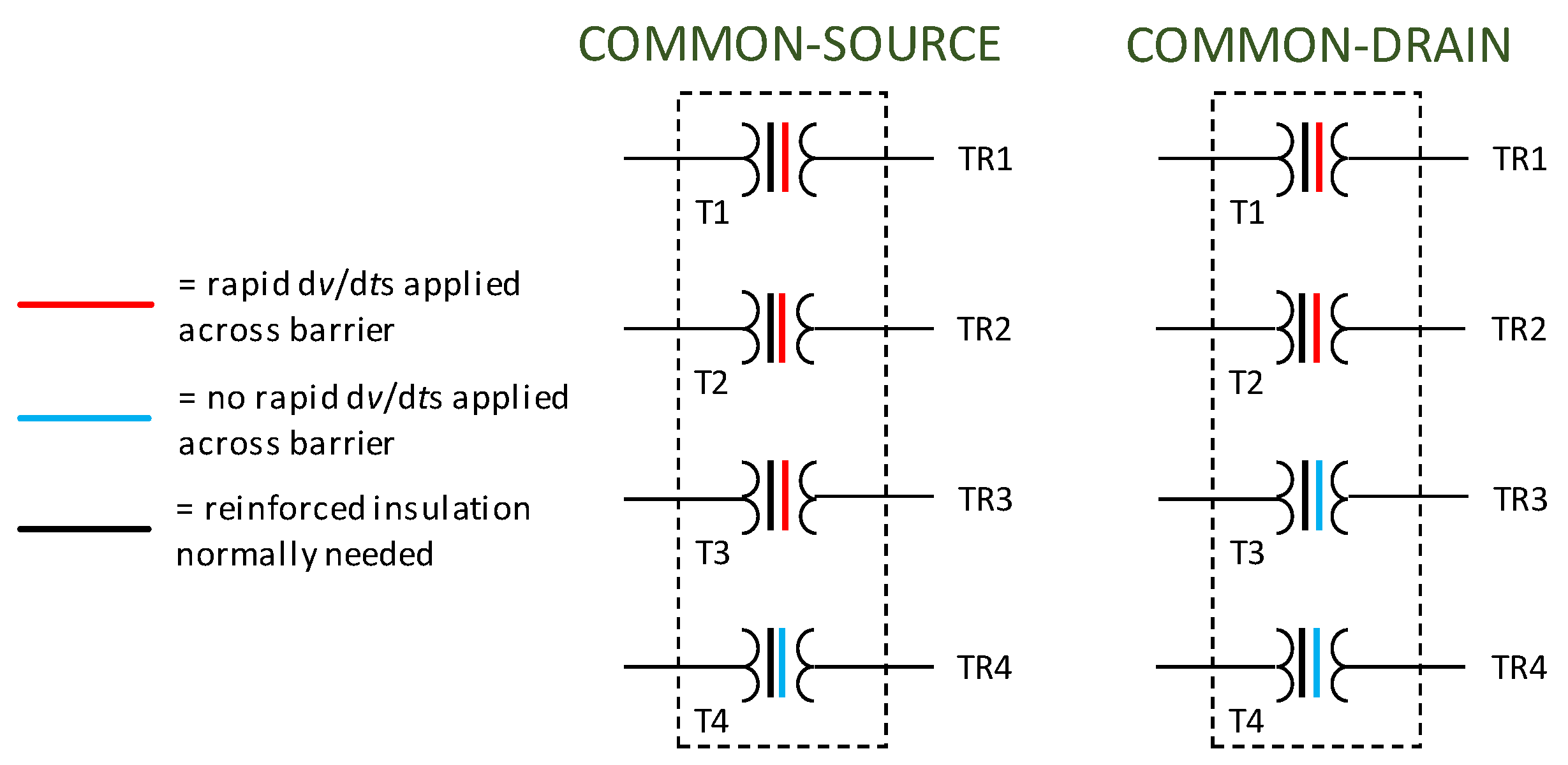
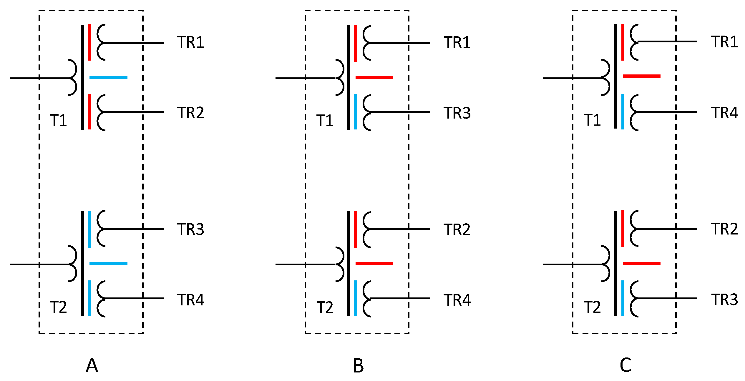
3.1. Transformer Arrangements

To avoid drive signal duty cycle restrictions dictated by the need for transformer core reset, the high-frequency carrier signal technique in [23] can be applied when transformers are used to transmit the power devices’ drive signals. To reduce cost, footprint area, and volume, the number of signal transmission transformers can be reduced by adapting [23] to use a carrier phase-switching technique [24]. With this technique, the drive signal’s carrier-frequency signal is synchronised to that transmitted by the associated power transmission transformer. By transmitting these signals in phase or in anti-phase, one transformer with two secondary windings can supply the signals for either of two power devices, provided the devices do not need to be held on at the same time, as is the case with a bridge-leg in a conventional two-level voltage source converter where this must be avoided.
Four devices need to be driven in the T-type converter. Ideally only two, instead of four, transformers could be used to transmit the drive signals. TR2 and TR3 normally have to be turned on at the same time for part of a switching cycle, and therefore must be driven by different transformers. Of the options in Figure 3 and Figure 4, Circuit “C” is therefore eliminated in each case. Circuit “A” in Figure 4 is preferred from the remaining options because of the absence of CM dv/dts between the secondary windings on both transformers, as was the case with the power transmission arrangement.

3.2. Signal Timing Issues

The upper four waveforms in Figure 5 show the standard situation where the bridge-leg is switching vout between VPOS and VMID. Normally TR2 is held on throughout the switching cycle. TR1 is driven on and off, with TR3 being driven with a complementary signal to that driving TR1, but with dead-times included. In Figure 5 it is assumed that the turn-on propagation delay tdon when a device is signalled on is negligible, but that the turn-off delay tdoff is significant. For this reason, a dead-time, or underlap time tu, must be imposed on the drive signals to avoid short-circuits.
An issue with using Circuit “A” instead of Circuit “B”, in either Figure 3 or Figure 4 for signal transmission, is that T1 cannot drive TR1 and TR2 on simultaneously to give the standard signals in Figure 5. However, it is observed that TR2 does not have to be on when TR1 is on, but only has to be on when TR1 is off. If iAC is negative, it flows through TR1 regardless of whether TR1 is on or off and whether TR2 is on or off. However, if iAC is positive, it flows through TR1, if TR1 is on but when TR1 is off, TR2 must be on to clamp vout to VMID and prevent vout making an excursion to VNEG.
Ideally, T1 would be controlled in such a way that TR2 is only driven on when TR1 is off. Normal gate drive signals can therefore be applied to the gate driver circuit, provided the circuit gates them so that turn-on of TR1 is prioritised over turn-on of TR2, whenever both are signalled on simultaneously.
A potential difficulty exists with timing tolerances whereby, if iAC is positive and TR1 turns off without TR2 already being on, vout will transition to VNEG for a short interval before TR2 turns on. Similarly, if TR2 turns off without TR1 already being on, vout will transition to VNEG for a short interval before TR1 turns on. Unlike the NPC converter, this does not result in an excessive voltage appearing across any of the power devices, but switching losses will be increased. A solution to this problem is to add a delay in TR1’s turn-off action after TR2 turns on, and a delay in TR2’s turn-off action after TR1 turns on. If tdoff is sufficiently greater than tdon, this inherently provides this function, and the lower four waveforms in Figure 5 illustrate this.
An essentially identical situation exists when iAC is negative and vout is being switched between VNEG and VMID. To prevent vout from making unwanted transitions to VPOS, there is a delay in TR4’s turn-off action after TR3 turns on, and a delay in TR3’s turn-off action after TR4 turns on.
By turning TR2 off when TR1 is on, and by turning TR3 off when TR4 is on, losses are incurred by charging and discharging the input capacitances of TR2 and TR3 more frequently than would otherwise be the case. Conversely, some losses are avoided. Consider the situation with a conventional gate driver when vout is being switched between VMID and VPOS. Normally TR2 is held on, and TR1 and TR3 switch complementarily. Apart from dead-times, two signal transformers are therefore energised at any one time in a conventional gate driver with magnetic signal isolation.
With respect to Circuit “A” in Figure 4, being used in the proposed scheme, two transformers (T1 and T2) are energised when vout is at VMID, but only one transformer, T1, is energised when vout is at VPOS. There is therefore a modest reduction in losses associated with supplying the transformers’ magnetising currents, and the currents they draw due to their core losses. A similar situation exists when vout is being switched between VMID and VNEG, and only one transformer, in this case T2, is energised when vout is at VNEG. However, although only one transformer is energised for part of the switching cycle, it is observed that when used with the phase-switching technique in [24], it has to drive two, and not one, load circuits, with the associated power losses.

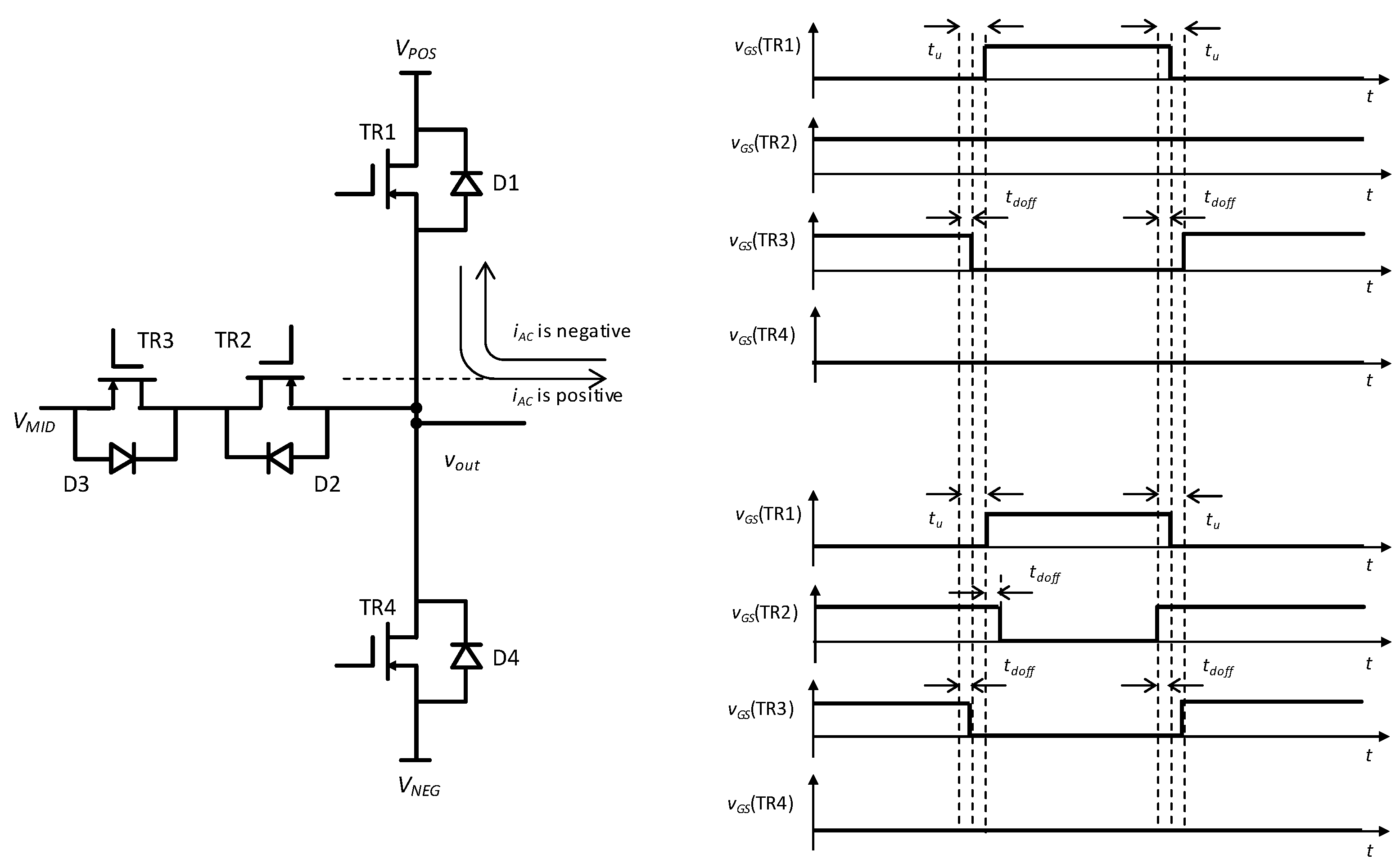
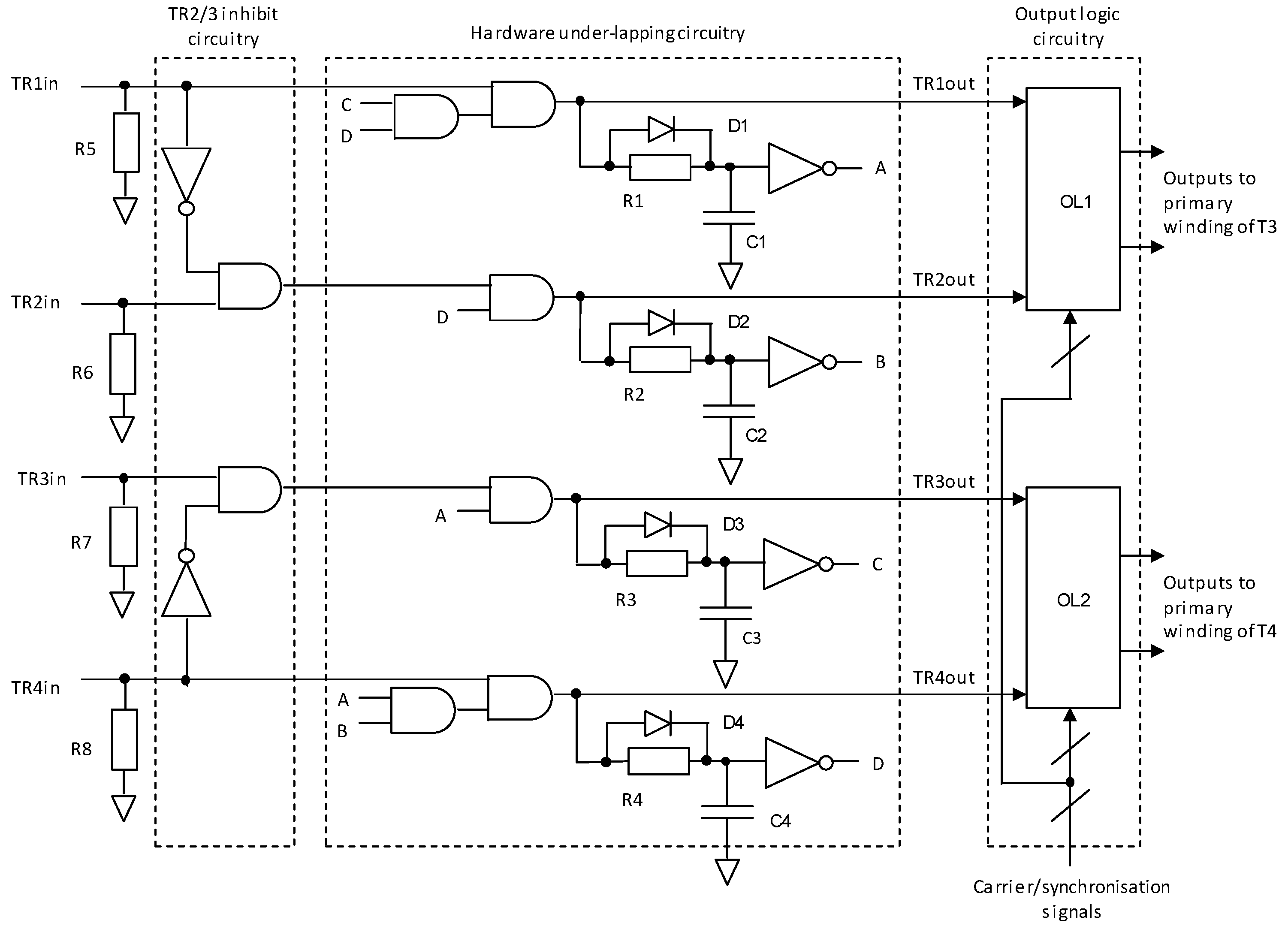
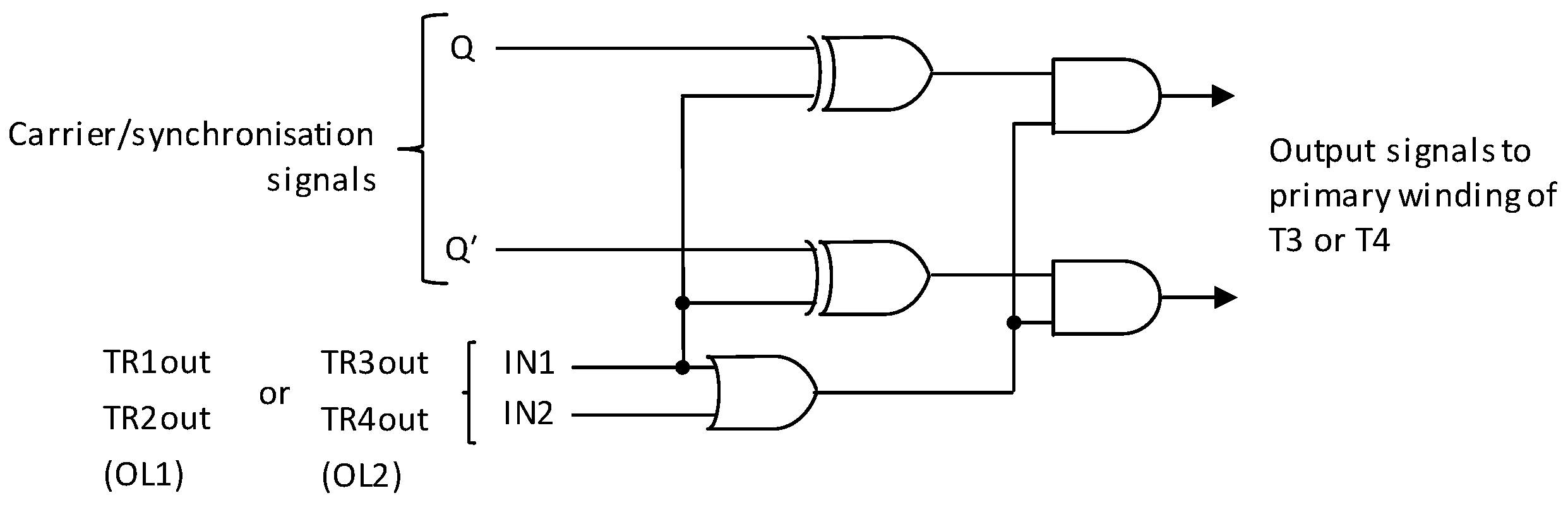
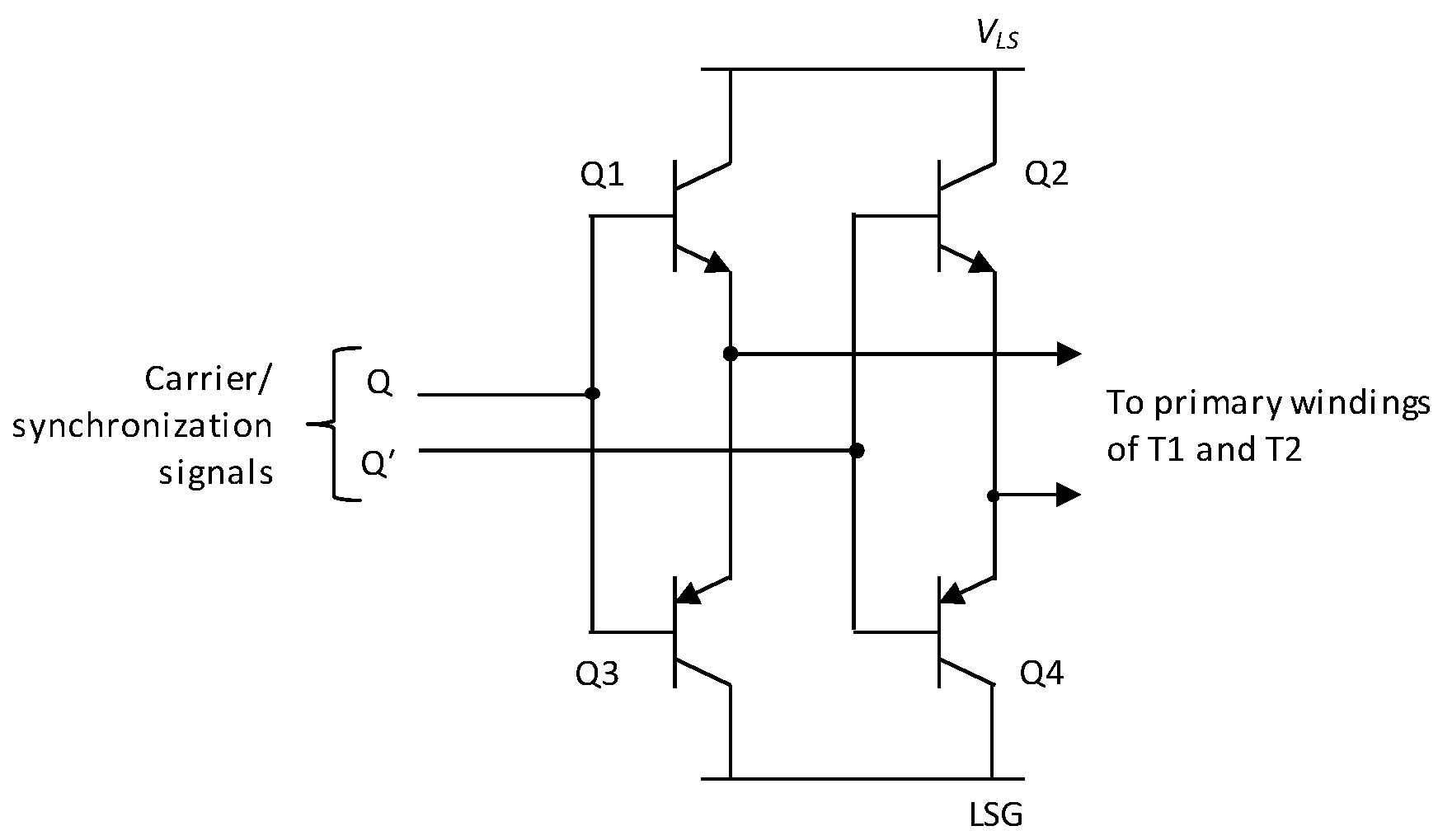
3.3. Proposed Low-Side Circuitry

Figure 6 shows the proposed low-side logic circuitry. The signal transformers are now designated T3 and T4 in this section, and subsequently in this article, as the power transformers have been designated T1 and T2. In addition to the hardware under-lapping circuitry normally found in a bridge-leg gate driver module, circuitry is included to inhibit TR2 from being turned on if TR1 is to be turned on, and to inhibit TR3 from being turned on if TR4 is to be turned on. Only four additional logic gates are required for this.
Each output signal TR1out-TR4out would normally enable a high-frequency carrier signal to be applied to an individual transformer. Instead, the output logic circuitry detailed in Figure 7 arranges whether drive signals are applied to T3 or T4, and defines their carrier signals’ phase relationships to that of the power transfer signal [24].
Specifically, if either IN1 or IN2 is high, the high-frequency carrier signal is applied to the related signal transformer’s primary winding. The phase relationship of the applied signal is defined according to whether it is TR1out or TR2out which is high in the case of output logic block OL1 in Figure 6, or TR3out or TR4out which is high in the case of output logic block OL2 in Figure 6. Signal Q and its complementary signal Q′ are derived from an oscillator within the low-side circuitry.
The oscillator produces a signal at twice the carrier frequency. This signal is applied to a D-type bi-stable logic gate which outputs Q and Q′ at the carrier frequency. This ensures that Q and Q′ each have a duty cycle of 50%, and thereby avoids saturation of the signal or power transformers’ cores, due to unequal positive-going and negative-going volt-second products being applied to their primary windings.

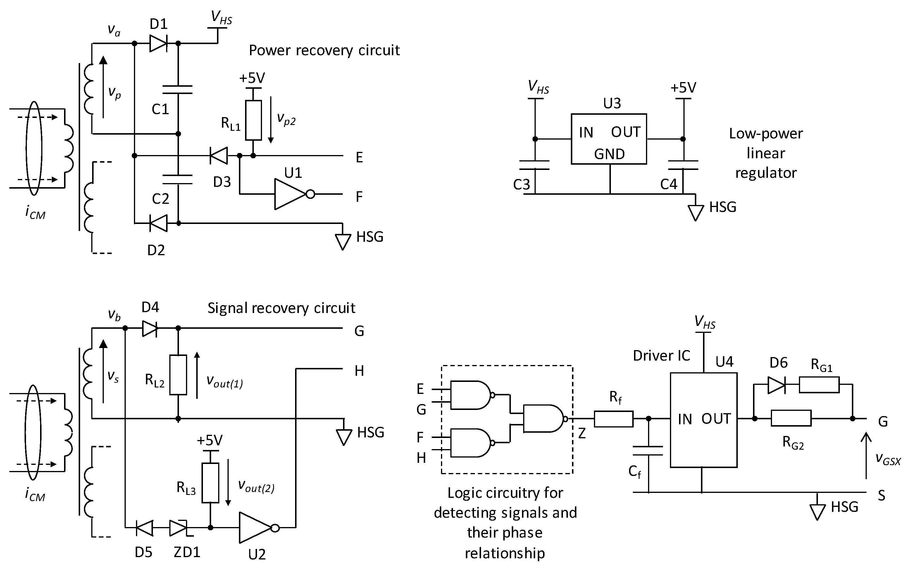
4. Overview of Proposed Circuit, and Details of High-Side Circuitry

Figure 8 shows a block diagram of the proposed circuitry where common-mode chokes, namely LCM1 and LCM2, can be included in series with T1 and T3, as these are the two transformers that are subject to dv/dts between their primary and secondary windings. Figure 9 shows the power recovery and signal recovery circuits within the local driver circuits in Figure 8. All of the local driver circuits are identical. The polarities of the connections made to their respective power and signal transformers ensure that they drive the associated power device on correctly in response to the signals TR1in-TR4in. The rectifier circuit used to recover power acts a voltage-doubler. The high-side voltage VHS produced by this circuit is nominally 15 V, which is suitable for driving cascode-connected normally-on SiC JFETs. The voltage-doubler arrangement minimises the number of secondary turns needed on the transformer, thus easing its construction.
A simple full-bridge circuit using BJTs in two emitter-follower bridge-legs, as shown in Figure 10, was used to drive T1 and T2. Two signals, namely E and F, are derived from the rectifier circuit by means of RL1, D3, and the inverter U1. 74AC-series logic gates, operating from a 5 V power supply, detect these signals and their phase relationships with signals G and H from the signal recovery stage. If G and H are present, and in the correct phase relationship with E and F, then the output voltage from the driver IC U4 goes high. 4000B-series gates were used in [24], and this logic series will operate directly from a supply voltage of 15 V, and is therefore compatible with the voltage typically used in a gate driver circuit. However, 74AC-series gates were used for two reasons. Firstly, the propagation delays are lower than those of 4000B-series gates. Secondly, the lower operating voltage means that they can be driven with smaller input voltages, and the signal transformer can consequently have a lower number of secondary turns, thereby easing its construction. The power consumption of 74AC-series circuitry is low, and the 5 V power supply for it can therefore readily be derived from the 15 V rail VHS by a physically small and low-cost linear regulator, U3 in Figure 9.
The signal recovery circuit in Figure 9 allows the signal transformer to be configured with one secondary winding for each device being driven. Unlike the full-wave rectifier which is normally used for signal recovery in gate driver applications, one end of this winding is connected directly to the high-side ground (HSG) connection. This arrangement was also used in [24] where the coupling transformers had high inter-winding capacitances. The technique allows CM currents through these capacitances to take a preferential route that bypasses the load resistances RL2 and RL3, and therefore reduces the magnitudes of spurious voltages developed across these resistances.
The Zener voltage of ZD1 is made approximately equal to 5 V, and operation of the signal recovery circuit is as follows. When vb is zero, G is pulled down to 0 V by RL2. The input to U2 is held at +5 V by RL3 and because of the Zener voltage drop of ZD1, vb cannot pull the input to U2 down to 0 V, and it remains at +5 V, and H is therefore 0 V. When vb is positive, G goes high, but H remains at 0 V. When vb is negative, G is pulled down to 0 V by RL2 and is therefore low. The negative voltage is dropped across the Zener voltage of ZD1, and the input of U2 is held at approximately 0 V, and H consequently goes high. D4 prevents vb from attempting to pull G down to a negative voltage when vb is negative.
As discussed in this section, the power transformers not only supply gate driver power, but also provide the reference signals E and F for comparison with the signals from the signal transformers. Apart from the lower number of secondary turns needed when compared to the full-wave rectifier circuit, another advantage of the voltage-doubler circuit is that one end of the applicable secondary winding is connected to the DC mid-point between C1 and C2 in the local driver circuit. This connection presents a preferential route for CM currents that bypasses the load resistance RL1. This reduces the magnitudes of spurious voltages developed across RL1, and thereby mitigates against consequent errors appearing in the signals E and F.
The output signal Z from the logic circuitry is applied to the low-pass filter formed with Rf and Cf. The output signal from the filter is applied to a driver IC, U4. This IC has an input voltage range compatible with the +5 V used by the logic circuitry, but is supplied from the higher voltage VHS. The filter removes any short voltage pulses appearing in Z due to mismatches in the timings of the signals received from the power and signal transmission stages.
With the addition of a diode and another resistor, this RC circuit can be used to introduce an asymmetric delay to make the turn-off delay slower than the turn-on delay if this is needed to meet the timing requirements described in Section 3.2. However, the arrangement of RG1, RG2, and D6 in Figure 9 is such that, apart from controlling the switching transients, it combines with the power device’s input capacitance to yield a gate-source voltage vGS fall-time to the power device’s gate-source threshold voltage VGS(th) that is longer than its rise-time to VGS(th).

5. Experimental Circuitry and Results

5.1. Hardware Configuration

The gate driver circuit in Figure 8 was prototyped on the double-sided printed circuit board (PCB) shown in the experimental rig, in Figure 11. The low-side supply voltage VLS was set at 5 V, and the high-side voltage VHS in each local driver circuit was nominally 15 V. The carrier frequency fc was 1 MHz.
Toroidal TN9/6/3 cores in 3F3 material were used for all the transformers, and to limit core losses, the peak allowable flux density excursion Bpk was set at 25 mT. For the power transformers, the number of primary turns N1pwr needed to meet the required Bpk is given by:
N 1 p w r = V L S 2 V B E 4 B p k A e f c
where VBE is the typical base-emitter voltage drop of each of the transistors in Figure 10, and Ae is the cross-sectional area of the core. Given the high gain of the transistors, the on-state collector-emitter voltage drop is taken as being the same as VBE. From the manufacturer’s data, VBE = 0.9 V and Ae = 4.44 mm2. Putting the data into (1) yields N1pwr = seven turns. The number of turns N2pwr on each of the secondary windings is given by:
N 2 p w r = V H S + 2 V f 2 N 1 p w r ( V i n 2 V B E )
where Vf is the forward voltage drop of each of the diodes D1 and D2 in Figure 9, and is taken as 0.7 V. Putting the data into (2) yields N2pwr = 18 turns.
For the signal transformers, the number of primary turns N1sig needed to meet the required Bpk is given by:
N 1 s i g = V L S 4 B p k A e f c .
Putting the data into (3) yields N1sig = 11 turns. The diodes D4 and D5 are taken as having a Vf of 0.7 V. The number of turns N2sig on each of the secondary windings is given by:
N 2 s i g = N 1 s i g ( V 2 + V f ) V L S
where V2 is the required output voltage and is set at 5 V. Putting the data into (4) yields N2sig = 13 turns. However, for two practical reasons the turns numbers of N1sig and N2sig were increased from their calculated values of 11 and 13, respectively, to 14 and 18, respectively. Firstly, the magnetising current required from the 74AC logic gates driving the signal transformers is reduced. Secondly, the power and signal transformers can be made identical if they carry two primary windings of seven turns. In the former case, the primary windings are connected in parallel, or one is not used, and in the latter case, they are connected in series. The peak magnetising current Im(pk) drawn by the signal transformers is given by:
I m ( p k ) = V L S 4 f c A L N 1 s i g 2
where AL is the core’s inductance factor specified by the manufacturer, and AL is 440 nH/turn2 for the TN9/6/3 core in 3F3 material. Putting the data into (5) yields Im(pk) = 14.5 mA.
All the primary windings for the transformers used 0.25 mm diameter polyurethane-insulated copper wire. All the secondary windings for the transformers used 0.2 mm diameter polyurethane-insulated copper wire. Reinforced insulation was not included between the transformers’ primary and secondary windings in the experimental circuit.
Details for the circuitry in Figure 6 were as follows. R1R8 = 1 kΩ. C1C4 were 330 pF ceramic capacitors. D1D4 were BAS16 diodes. Decoupling capacitance was included across the 5 V supply rail VLS, but is not shown in Figure 6, for clarity. Details for the circuitry in Figure 9 were as follows. RL1RL3 = 1 kΩ. RG1 and RG2 = 22 Ω. Rf = 150 Ω. C1C4 were 100 nF, ceramic capacitors. Cf was 660 pF, being formed with two 330 pF ceramic capacitors, in parallel. D1D5 were BAS16 diodes. ZD1 was an AZ23C4V7-7-F Zener diode. U3 was an UA78L05ACDRG4 IC, and U4 was an IXDN614SI IC. In Figure 10, Q1 = Q2 = ZTX651, and Q3 = Q4 = ZTX 751. All the logic gates in Figure 6, Figure 7 and Figure 9 were 74AC-series types. The common-mode chokes LCM1 and LCM2, shown in Figure 8, were each formed with an R6.3/3.8/2.5 core in N87 material carrying a 14-turn bifilar winding of 0.25 mm diameter polyurethane-insulated copper wire.

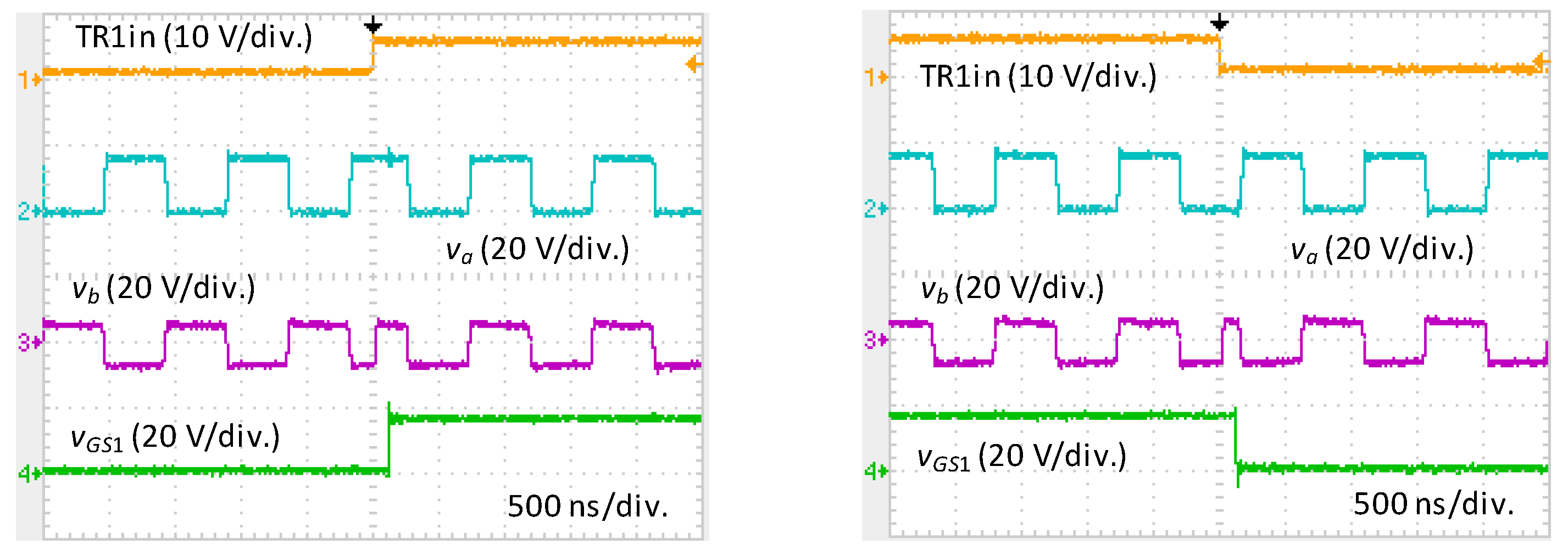
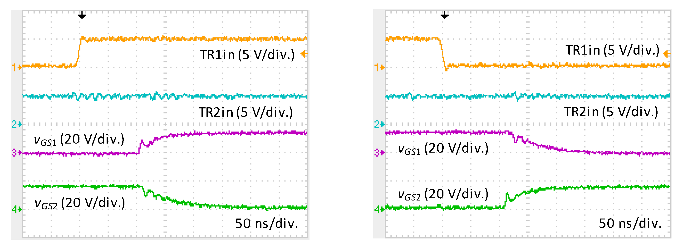
5.2. Propagation Delays and Power Consumption

Without any power devices being connected to the driver circuit, waveforms at turn-on and turn-off are shown in Figure 12. The voltages va and vb are measured with respect to HSG. LCM1 and LCM2 were not initially included. The propagation delay between TR1in and vGS1 at turn-on was measured at a maximum of 144 ns, with a jitter range of 28 ns, and at turn-off, was measured at a maximum of 152 ns, with a jitter range of 36 ns.
A UJ3C120040K3S device and a UF3C065040K3S device were then connected in positions TR1 and TR2, respectively. These devices are cascode-connected normally-on SiC JFETs, which have a normally-off functionality. The drain and source terminals of each JFET were connected together for this test. TR1 was signalled on and off, and TR2 was signalled on at a duty cycle of 100%. Waveforms are shown in Figure 13. Although TR2 is signalled on at a duty cycle of 100%, it is seen that it is inhibited from turning on when TR1 is also on. As described in Section 3.2, overlapping is required between the gate drive signals applied to TR1 and TR2, and between the gate drive signals applied to TR3 and TR4. The VGS(th) voltage of cascode-connected normally-on JFETs is typically between 4 V and 6 V. As discussed in Section 4, the circuit naturally introduces the required overlapping due to the difference between the time taken for vGS to rise to VGS(th) at turn-on, and the time taken for vGS to fall to VGS(th) at turn-off. From the waveforms in Figure 13, the overlap delays at turn-on and turn-off of TR1 are both estimated at approximately 50 ns. The power consumption of the test circuit was measured at 1.475 W when operating at 75 kHz, signalling TR1 on at a duty cycle of 50%, and signalling TR2 on at a duty cycle of 100%.

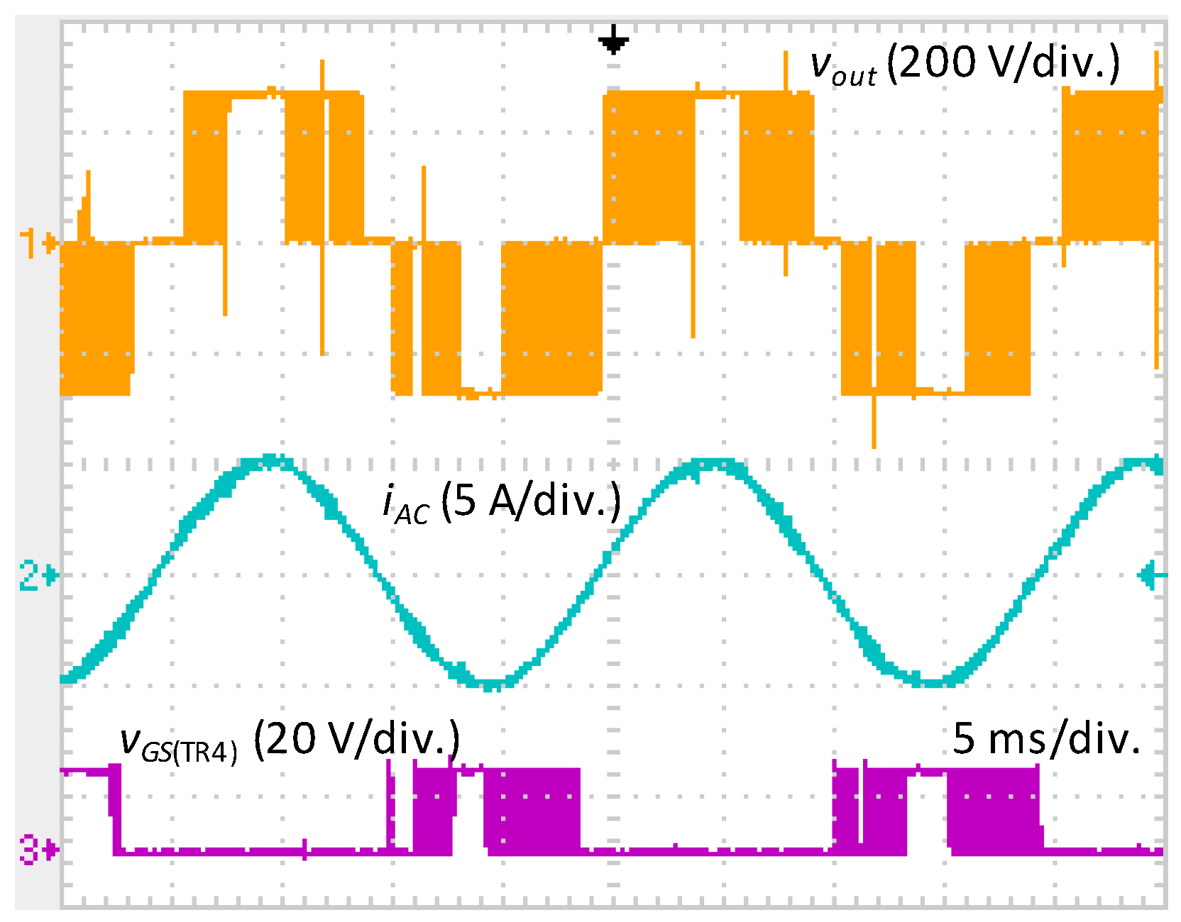
5.3. Operation with a T-Type Bridge-Leg

The circuit in Figure 11 was used to drive the cascode-connected normally-on SiC JFETs in a T-type converter bridge-leg configured in the CD arrangement in Figure 1. The bridge-leg was supplied from a DC voltage of 540 V (±270 V). TR1 and TR4 were UJ3C120040K3S devices rated at 1200 V, and TR2 and TR3 were UF3C065040K3S devices rated at 650 V.
The SiC MOSFET is commonly used in fast-switching applications, but has gate-drive challenges, if simultaneous conduction (“crosstalk”), due to dv/dt-induced turn-on, is to be avoided in bridge-legs [25,26]. A carefully regulated off-state gate-source voltage is required to protect against dv/dt-induced turn-on whilst not over-stressing the gate-source junction. Trans-conductance is low compared to silicon MOSFETs, and a carefully regulated on-state gate-source voltage is also required to reduce conduction losses whilst, again, not over-stressing the gate-source junction.
The SiC BJT is also a fast-switching device, but does not have an intrinsic diode, and does not conduct effectively in reverse. It has a robust base-drive requirement, and dv/dt-induced turn-on can be readily avoided if a negative off-state base-emitter voltage is applied [27]. However, unlike its voltage-driven SiC counterparts (the MOSFET and JFET) it is current-driven and needs a significant steady-state base current to hold it on.
The cascode-connected normally-on SiC JFET [28,29], as used here, has a robust gate drive requirement as the external gate terminal being driven is that of a low-voltage silicon MOSFET, and simultaneous conduction is not problematic, even when only using a unipolar gate drive voltage. The cascode-connected normally-on SiC JFET can operate satisfactorily over a wide applied external gate-source voltage range.
To minimise EMI, small ferrite beads [30] were located around the conductor connected to the drain of TR4, and the conductor carrying the power connection to the source of TR1. Also, a snubber consisting of a 1 nF, 1 kV ceramic capacitor in series with two 15 Ω carbon resistors in parallel was connected between vout and VMID. Local film and ceramic decoupling capacitors were connected between VPOS and VMID, and between VMID and VNEG. The heatsink on which the power devices were mounted was connected to VMID.
The bridge-leg was used to output a sinusoidal current of 3.52 A at a base-frequency of 50 Hz into an RL series load at a near-unity power factor. The switching frequency was 75 kHz, and the switching signals were produced on a Texas Instruments LaunchPad development PCB. A simple pulse width modulation scheme was used, but more sophisticated schemes can be implemented such as that in [31]. LCM1 and LCM2 were now included. Figure 14 shows the main waveforms, namely vout and iAC, from the bridge-leg and for reference, the gate-source voltage waveform vGS(TR4) applied to TR4.

6. Discussion

6.1. Power Transmission Stage

Advantages of using the emitter-follower stage, shown in Figure 10, are that it is simple, propagation delays are low, and that it inherently avoids shoot-through currents. Disadvantages are that its efficiency is low in this application due to the VBE voltages of the transistors being large, in proportion to VLS. Also, the secondary voltage magnitude is disproportionately affected by variations in the primary supply voltage due to the VBE voltages of the transistors. However, as discussed in Section 5, the gate-drive requirement of the cascode-connected normally-on SiC JFET is tolerant of a wide voltage range, and a precisely controlled gate driver supply voltage is therefore not mandatory. Although efficiency is low, this is not necessarily problematic because the gate driver circuit’s secondary power consumption is, in any case, low due to the power devices’ low input capacitances.

6.2. Timing Issues

The time-constant formed by Rf and Cf in the low-pass filter, in Figure 9, was set at a conservatively high value in order to eliminate spurious pulses. However, this increases the propagation delays. The minimum time-constant necessary to ensure elimination of these pulses will be investigated further. Also, signal jitter is normally an inherent effect of the high-frequency carrier technique, and the effect of this on EMI is also to be investigated.

6.3. Signal Recovery Stages

As shown in Figure 9, the signal recovery stages are configured to have a high immunity to erroneously detecting signals produced by CM currents. However, only the driver circuits for TR1 and TR2 are expected to be susceptible to this, and high dv/dts do not appear between secondary windings on the shared transformers. Nonetheless, for simplicity, recovery circuits with high CM immunity are still used in all the driver circuits. This also enables the driver circuit to be more readily adapted for diode-clamped NPC converters if required, where dv/dts are inevitably present between the windings on the shared transformers.

6.4. Use of Magnetic Coupling for Signal Transmission

Compared to opto-couplers and proprietary signal isolation technologies, the cost of the raw materials used in the signal transformers is low, particularly as there are only two needed, but assembly costs have to be accounted for. However, if the power devices were to be driven with individual transformers for each signal and power transmission channel, eight transformers would be needed. Moreover, four of the transformers would present routes for CM currents between the converter’s high-side and low-side circuitry, whereas only two do this in the proposed scheme.

7. Conclusions

A gate driver circuit with all-magnetic isolation has been presented for driving SiC power semiconductor devices in a three-level T-type bridge-leg. Only four transformers are used for supplying all four devices in the bridge-leg with local floating power supplies and gate-drive signals, and the arrangement addresses common-mode interference due to the rapid voltage changes applied across the transformers’ parasitic inter-winding capacitances. All of the transformers can have an identical construction. The circuit has been demonstrated when driving cascode-connected normally-on SiC JFETs at 75 kHz in a 540 V (±270 V) T-type bridge-leg. Further investigation will include assessing the feasibility of operating the circuit at higher power device switching frequencies, using planar transformers, and realising the proposed circuity in the form of application-specific integrated circuits.

Author Contributions

Conceptualization, N.M.; methodology, N.M.; software, D.V., R.P.-A. and S.W.; validation, N.M. and D.V.; investigation, N.M., D.V., R.P.-A., S.W. and R.P.; writing—original draft preparation, N.M.; writing—review and editing, N.M., D.V., R.P.-A., S.W., R.P., D.H. and B.W.W.; visualization, N.M., D.V., R.P.-A., S.W. and R.P.; supervision, N.M., D.H. and B.W.W.; project administration, N.M., D.H. and B.W.W.; funding acquisition, N.M. and D.H. All authors have read and agreed to the published version of the manuscript.

Funding

This research was funded by the UK Engineering and Physical Sciences Research Council (EPSRC) under grant EP/R029504/1 (‘Quietening ultra-low-loss SiC & GaN waveforms’).

Data Availability Statement

Data sharing is not applicable to this article.

Conflicts of Interest

The authors declare no conflict of interest.

References

  1. Kouro, S.; Malinowski, M.; Gopakumar, K.; Pou, J.; Franquelo, L.G.; Wu, B.; Rodriguez, J.; Pérez, M.A.; Leon, J.I. Recent advances and industrial applications of multilevel converters. IEEE Trans. Ind. Electron. 2010, 8, 2553–2579. [Google Scholar] [CrossRef]
  2. 3L NPC & TNPC Topology, Application Note AN11001. Available online: www.semikron.com (accessed on 1 October 2022).
  3. Zhang, Z.; Anthon, A.; Andersen, M.A.E. Comprehensive loss evaluation of neutral-point-clamped (NPC) and T-type three-level inverters based on a circuit level decoupling modulation. In Proceedings of the 2014 International Power Electronics Applications Conference and Exposition, Shanghai, China, 5–8 November 2014; pp. 82–87. [Google Scholar]
  4. Anthon, A.; Zhang, Z.; Andersen, M.A.E.; Franke, T. Efficiency investigations of a 3 kW T-type inverter for switching frequencies up to 100 kHz. In Proceedings of the International Power Electronics Conference, Hiroshima, Japan, 18–21 May 2014; pp. 78–83. [Google Scholar]
  5. Schweizer, M.; Kolar, J.W. Design and implementation of a highly efficient three-level T-type converter. IEEE Trans. Power Electron. 2013, 28, 899–907. [Google Scholar] [CrossRef]
  6. Sun, B.; Burgos, R.; Boroyevich, D. Ultralow input–output capacitance PCB-embedded dual-output gate-drive power supply for 650 V GaN-based half-bridges. IEEE Trans. Power Electron. 2019, 34, 1382–1393. [Google Scholar] [CrossRef]
  7. Anurag, A.; Acharya, S.; Prabowo, Y.; Gohil, G.; Bhattacharya, S. Design considerations and development of an innovative gate driver for medium voltage power devices with high dv/dt. IEEE Trans. Power Electron. 2019, 34, 5256–5267. [Google Scholar] [CrossRef]
  8. Rothmund, D.; Bortis, D.; Kolar, J.W. Highly compact isolated gate driver with ultrafast overcurrent protection for 10 kV SiC MOSFETs. CPSS Trans. Power Electron. Appl. 2018, 3, 278–291. [Google Scholar] [CrossRef]
  9. She, X.; Datta, R.; Harfman Todorovic, M.; Mandrusiak, G.; Dai, J.; Frangieh, T.; Cioffi, P.; Rowden, B.; Mueller, F. High performance silicon carbide power block for industry applications. IEEE Trans. Ind. Appl. 2017, 53, 3738–3747. [Google Scholar] [CrossRef]
  10. Mao, S.; Popovic, J.; Ferreira, J.A. Switching characterization and low inter-winding capacitance gate driver power supply of 1200 V SiC MOSFET for the 300 kHz 10 kW inverter. In Proceedings of the 1st Workshop on Wide Bandgap Power Devices and Applications in Asia, Xi’an, China, 16–18 May 2018; pp. 270–275. [Google Scholar]
  11. Hui, S.Y.; Tang, S.C.; Chung, H.S.-H. Optimal operation of coreless PCB transformer-isolated gate drive circuits with wide switching frequency range. IEEE Trans. Power Electron. 1999, 14, 506–514. [Google Scholar] [CrossRef]
  12. Gui, Z.; Li, H.; Cheetham, P. A very-high-frequency isolated gate driver power supply using solid dielectrics for medium voltage MOSFETs. In Proceedings of the IEEE Applied Power Electronics Conference and Exposition, Houston, TX, USA, 20 March 2022; pp. 1394–1399. [Google Scholar]
  13. Gottschlich, J.; Schäfer, M.; Neubert, M.; De Doncker, R.W. A galvanically isolated gate driver with low coupling capacitance for medium voltage SiC MOSFETs. In Proceedings of the 18th European Conference on Power Electronics Applications, Karlsruhe, Germany, 5–9 September 2016. [Google Scholar]
  14. Hu, J.; Wang, J.; Burgos, R.; Wen, B.; Boroyevich, D. High-density current-transformer based gate-drive power supply with reinforced isolation for 10 kV SiC MOSFET modules. IEEE J. Emerg. Sel. Top. Power Electron. 2020, 8, 2217–2226. [Google Scholar] [CrossRef]
  15. Gill, L.; Ikari, T. CM filter analysis and mitigation of common mode current in SiC MOSFET gate driver power supply. In Proceedings of the 2018 IEEE International Conference on Electrical Systems for Aircraft, Railway, Ship Propulsion and Road Vehicles & International Transportation Electrification Conference, Nottingham, UK, 7–9 November 2018. [Google Scholar]
  16. Hazra, S.; Madhusoodhanan, S.; Moghaddam, G.K.; Hatua, K.; Bhattacharya, S. Design considerations and performance evaluation of 1200-V 100-A SiC MOSFET-based two-level voltage source converter. IEEE Trans. Ind. Appl. 2016, 52, 4257–4268. [Google Scholar] [CrossRef]
  17. Nguyen, V.-S.; Kerachev, L.; Lefranc, P.; Crebier, J.-C. Architecture characterization and analysis of an innovative gate driver and power supplies architecture for HF power devices with high dv/dt. IEEE Trans. Power Electron. 2017, 32, 6079–6090. [Google Scholar] [CrossRef]
  18. Alves, L.F.S.; Lefranc, P.; Jeannin, P.-O.; Sarrazin, B. A new gate drive power supply configuration for common mode conducted EMI reduction in phase-shifted full-bridge converter. IEEE Trans. Power Electron. 2021, 36, 4081–4090. [Google Scholar] [CrossRef]
  19. Zhang, X.; Li, H.; Brothers, J.A.; Fu, L.; Perales, M.; Wu, J.; Wang, J. A gate drive with power over fiber-based isolated power supply and comprehensive protection functions for 15-kV SiC MOSFET. IEEE J. Emerg. Sel. Top. Power Electron. 2016, 4, 946–955. [Google Scholar] [CrossRef]
  20. Pan, J.; Qi, F.; Cai, H.; Xu, L. Efficiency and electromagnetic interference analysis of wireless power transfer for high voltage gate driver application. In Proceedings of the IEEE 9th Energy Conversion Congress and Exposition, Milwaukee, WI, USA, 18–22 September 2016. [Google Scholar]
  21. Falck, J.S.; Felgemacher, C.; Rojko, A.; Liserre, M.; Zacharias, P. Reliability of power electronics systems: An industry perspective. IEEE Ind. Electron. Mag. 2018, 12, 24–35. [Google Scholar] [CrossRef] [Green Version]
  22. Waffler, S.; Round, S.D.; Kolar, J.W. High temperature (>200°C) isolated gate drive topologies for silicon carbide (SiC) JFET. In Proceedings of the IEEE 34th Annual Industrial Electronics Conference, Orlando, FL, USA, 10–13 November 2008; pp. 2867–2872. [Google Scholar]
  23. Turnbull, F.G. A carrier frequency gating circuit for static inverters, converters, and cycloconverters. IEEE Trans. Magn. 1966, 2, 14–17. [Google Scholar] [CrossRef]
  24. McNeill, N.; Holliday, D.; Mellor, P.H. Alleviating common-mode interference effects in phase-switched power device gate driver circuit. IET Electron. Lett. 2008, 44, 880–881. [Google Scholar] [CrossRef]
  25. Zhang, Z.; Wang, F.; Tolbert, L.M.; Blalock, B.J. Active gate driver for crosstalk suppression of SiC devices in a phase-leg configuration. IEEE Trans. Power Electron. 2014, 29, 1986–1997. [Google Scholar] [CrossRef]
  26. Khanna, R.; Amrhein, A.; Stanchina, W.; Reed, G.; Mao, Z.-H. An analytical model for evaluating the influence of device parasitics on Cdv/dt induced false turn-on in SiC MOSFETs. In Proceedings of the IEEE 28th Annual Applied Power Electronics Conference and Exposition, Long Beach, CA, USA, 17–21 March 2013; pp. 518–525. [Google Scholar]
  27. McNeill, N.; Jin, B.; Yuan, X.; Laird, I. Evaluation of the off-state base-emitter voltage requirement of the SiC BJT with a regenerative proportional base driver circuit and their application in an inverter. IEEE Trans. Ind. Electron. 2020, 67, 7179–7189. [Google Scholar] [CrossRef] [Green Version]
  28. Ortiz-Gonzalez, J.; Wu, R.; Jahdi, S.; Alatise, O. Performance and reliability review of 650 V and 900 V silicon and SiC devices: MOSFETs, cascode JFETs and IGBTs. IEEE Trans. Ind. Electron. 2020, 67, 7385–7395. [Google Scholar]
  29. Wu, R.; Ortiz-Gonzalez, J.; Davletzhanova, Z.; Mawby, P.A.; Alatise, O. The potential of SiC cascode JFETs in electric vehicle traction inverters. IEEE Trans. Transp. Electrif. 2019, 5, 1349–1359. [Google Scholar] [CrossRef] [Green Version]
  30. Josifović, I.; Popović-Gerber, J.; Ferreira, J.A. Improving SiC JFET switching behavior under influence of circuit parasitics. IEEE Trans. Power Electron. 2012, 27, 3843–3854. [Google Scholar] [CrossRef]
  31. Pou, J.; Zaragoza, J.; Rodriguez, P.; Ceballos, S.; Sala, V.M.; Burgos, R.P.; Boroyevich, D. Fast-processing modulation strategy for the neutral-point-clamped converter with total elimination of low-frequency voltage oscillations in the neutral point. IEEE Trans. Ind. Electron. 2007, 54, 2288–2294. [Google Scholar] [CrossRef]
Figure 1. T-type converter bridge-leg shown with the central devices, TR2 and TR3, connected in common-source and common-drain configurations. JFETs are shown as the power devices. The diodes depicted are not discrete devices, but represent the JFETs’ equivalent intrinsic diode functionality when reverse-biased.
Energies 16 01226 g001
Figure 2. Gate driver power transmission configurations with a single transformer for each device, with CS and CD arrangements.
Energies 16 01226 g002
Figure 3. Gate driver power transmission configurations using two transformers with CS arrangement.
Energies 16 01226 g003
Figure 4. Gate driver power transmission configurations using two transformers with CD arrangement.
Energies 16 01226 g004
Figure 5. Waveforms. The upper four show the standard drive signals applied when switching between VPOS and VMID in a three-level bridge-leg. The lower four show the signals applied using the proposed scheme. TR2 has to be turned on when TR1 is off to clamp vout to VMID and prevent it from making excursions to VNEG whenever iAC is positive.
Energies 16 01226 g005
Figure 6. Low-side logic circuitry. The signal transformers are designated T3 and T4 in this figure as the power transformers have been designated T1 and T2.
Energies 16 01226 g006
Figure 7. Logic circuitry within each of the output logic blocks OL1 and OL2 in Figure 6.
Energies 16 01226 g007
Figure 8. Block diagram of the proposed gate driver circuit.
Energies 16 01226 g008
Figure 9. Arrangements for recovering the power and gate drive signals within each of the local driver circuits in Figure 8.
Energies 16 01226 g009
Figure 10. Full-bridge circuit used for driving transformers T1 and T2 in Figure 8. The complementary signals Q and Q′ driving the emitter-follower legs are derived from the same oscillator producing the carrier-frequency signal used for transmitting the gate drive signals in Figure 7.
Energies 16 01226 g010
Figure 11. Experimental rig. Reinforced insulation was not included between the transformers’ primary and secondary windings in the experimental gate driver circuit.
Energies 16 01226 g011
Figure 12. Waveforms showing behaviour at turn-on and turn-off of TR1. (Left) turn-on. (Right) turn-off. va and vb were both measured with respect to HSG in Figure 9. The change in phase of vb with respect to va is seen in each case. When TR1 is being signalled off, vb is still active as TR2 is being driven on.
Energies 16 01226 g012
Figure 13. Waveforms from channels driving TR1 and TR2. (Left) TR1 turn-on. (Right) TR1 turn-off.
Energies 16 01226 g013
Figure 14. Waveforms from T-type bridge-leg configured in the common-drain connection in Figure 1 when it is being driven by the gate driver circuitry in Figure 8 and Figure 11.
Energies 16 01226 g014
Table 1. Principle symbols and abbreviations.
Symbol or AbbreviationDescription
AeEffective area of magnetic core (m2)
ALInductance factor of magnetic core (H/turn2)
BpkPeak magnetic flux density (T)
CDCommon-drain
CMCommon-mode
CSCommon-source
fcCarrier frequency (Hz)
Im(pk)Peak magnetising current drawn by transformer (A)
N1pwrNumber of turns on primary winding of power transformer
N1sigNumber of turns on primary winding of signal transformer
N2pwrNumber of turns on each secondary winding of power transformer
N2sigNumber of turns on each secondary winding of signal transformer
VBEBase-emitter voltage drop of BJT when conducting (V)
VfForward voltage drop of diode when conducting (V)
vGSGate-source voltage applied to MOS-gated device (V)
VGS(th)Threshold gate-source voltage of MOS-gated device (V)
Disclaimer/Publisher’s Note: The statements, opinions and data contained in all publications are solely those of the individual author(s) and contributor(s) and not of MDPI and/or the editor(s). MDPI and/or the editor(s) disclaim responsibility for any injury to people or property resulting from any ideas, methods, instructions or products referred to in the content.

