Abstract
This study proposed an isolated three-port bidirectional resonant converter that combines 2C3L and 2C2L resonant circuits for application in power dispatching. The proposed converter improves the bidirectional power dispatch capabilities of conventional three-port converters and utilizes different resonant converters to complete the energy charge–discharge through ports of different voltage levels. By modulating the frequency alone, bidirectional power regulation and electrical isolation were achieved among the three ports with different voltage levels. The converter involves the use of resonance techniques to enable the power switch to perform soft switching during bidirectional power transmissions, reducing switching loss and electromagnetic interference. The system control of the circuit was a Texas Instruments TMS320F28335 microcontroller. By simulating a DC grid port with a fixed voltage of 400 V, a vehicle battery port with a variable voltage of 280–403 V, and a battery charging port with a variable voltage of 180–213 V, an experimental platform with a rated output of 3 kW was built to determine the accuracy of the proposed theoretical analysis and design method.
1. Introduction
Electric vehicle power systems of the future must be able to acquire power from stored energy in the battery in addition to electrical energy from the electric grid. In some cases, the electric car must feed power from its battery into the electric grid. A three-port power converter must be developed to handle the power dispatch between a DC grid port, vehicle battery port [1,2,3], and battery bank port [4,5,6] to achieve peak shaving and to balance the operating reserve between the power generation end and the user end.
Resonant converters feature soft switching, which is one advantage to reducing power switching loss. Common resonant converters include LC resonant converters, LCC resonant converters, and LLC resonant converters, with LLC resonant converters having the most popular topology [7,8]. The soft switching technology of LLC resonant converters can be used to lower the electromagnetic interference and switching loss produced by power switches, thereby increasing the converter efficiency. However, in the reverse mode, the voltage gain is limited to unity gain, which hinders the performance of reverse-boost operations and bidirectional power operations. As a result, LLC resonant converters are not suitable for bidirectional transmission.
Resonant converters suitable for the bidirectional transmission of energy can be largely distinguished into 2C3L resonant converters and 2C2L resonant converters. A 2C3L resonant converter features a circuit topology comprising two capacitors and three inductors, which will hereafter be referred to as a 2C3L resonant circuit. The circuit topology of a 2C2L resonant converter comprises two capacitors and two inductors, referred to as a 2C2L resonant circuit throughout the rest of this paper. These two resonant architecture types compensate for the shortcomings of conventional LLC resonant converters that cannot be boosted in reverse mode. A 2C3L topology features the same equations for forward and reverse voltage gains and is therefore easier to design and is suitable for two ports with similar voltage levels; however, it uses more components than that of a 2C2L topology. Although a 2C2L topology does not have the same equations for forward and reverse voltage gains, it offers more design freedom and greater voltage gains in reverse mode. In addition, when used in large-scale voltage reduction scenarios, a 2C2L topology can decrease the difficulty of winding a high-turn transformer.
The authors of [9,10,11,12] proposed adding LC resonant components to Port 1 and Port 2 of an isolated three-power port converter (Figure 1). The advantage of this configuration is that when energy is transmitted to Port 3 either from Port 1 or Port 2, an LLC resonant topology forms, resulting in wide-range voltage output. Between Port 1 and Port 2, a 2C3L bidirectional resonant topology forms and has bidirectional wide-range voltage output and the same voltage gain equation in forward and reverse modes. However, when energy is transmitted from Port 3 to either Port 1 or Port 2, the same shortcoming occurs, namely, that the resonant network is routed from the original LLC resonant circuits to the LC resonant circuit (as described earlier), and a phase shift controller or pulse modulator must be added to achieve wide-voltage input and output and drastically increase the control complexity.
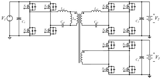
Figure 1.
Isolated three-port converter proposed in [9,10].
This paper proposed a concrete solution for the inability to meet the energy conversion requirements during a bidirectional transmission of energy solely through a single-controller mode. An isolated three-power port converter combining 2C3L and 2C2L resonant circuits was developed as part of this solution. Resonant components were added to Port 3, and the wide-range voltage output requirements and the product requirements, namely, high performance, high power density, and low cost, were met through appropriate design parameters, an uncomplicated converter architecture, and simple system controls. The proposed solution addresses the original need to handle energy transmissions between the three ports through three separate DC–DC bidirectional converters, which compels the system to include multiple converters, resulting in a bulky architecture and high cost.
2. Introducing the Circuit Architecture and Its Features
2.1. Circuit Architecture
The isolated three-port power converter combining 2C3L and 2C2L resonant circuits provides bidirectional energy transfers among the DC energy grid port, battery bank port, and vehicle battery port (Figure 2). The converter has six power conversion modes: from the DC grid port to the vehicle battery port (G2V mode), from the vehicle battery port to the DC grid port (V2G mode), from the vehicle battery port to the battery bank port (V2B mode), from the battery bank port to the vehicle battery port (B2V mode), from the DC grid port to the battery charging port (G2B mode), and from the battery charging port to the DC grid port (B2G mode). Table 1 lists the six power conversion modes of this bidirectional converter. In Figure 2, the converter combines a triple-active bridge converter architecture with 2C3L and 2C2L resonant topologies, creating an isolated converter with three power ports and bidirectional resonance. This design improves the bidirectional power modulating capabilities of conventional three-port converters, enabling the converter to utilize different resonant converters when charging or discharging through ports with different voltage levels. This converter can achieve bidirectional power modulation and electrical isolation between the three power ports with different voltage levels through frequency modulation alone. In addition, it utilizes resonance techniques to enable the power switch to achieve soft switching during bidirectional power transmission, thus reducing switching loss and increasing the power conversion efficiency [13].
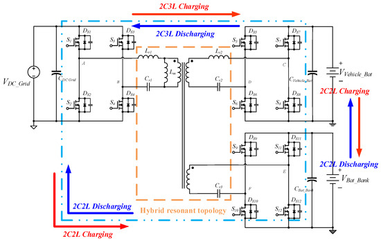
Figure 2.
Three-port power conversation with 2C3L and 2C2L resonant circuits.

Table 1.
Six power conversion modes of the converter.
2.2. Circuit Gains in the Resonant Converter
Figure 3 depicts the voltage gain characteristics of the resonant converter. The gains vary in size with the switching frequency fs and can be divided into three regions. When the circuit is operating in Region I, the power switch only involves zero-voltage switching (ZVS). When the circuit is operating in Region II, in addition to ZVS due to the power switch, the secondary rectifying switch can achieve zero-current switching (ZCS), which greatly reduces the power loss and increases the circuit conversion efficiency. When the circuit is operating in Region III, the voltage gains fluctuate considerably. Thus, the circuit is not suited to the modulation of input- and output wide-range voltage, and operations in this region should be avoided. Because of their symmetry, bidirectional symmetrical 2C3L resonant circuits demonstrate both ZVS and ZCS when operating in either the forward mode or reverse mode. In this figure, the full load is 7.5 A, 25% is 1.875 A, and the maximum and minimum gain refer to the upper and lower limits of the voltage gain, indicating that the required voltage gain can be achieved under different loads.
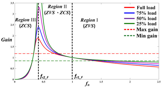
Figure 3.
Voltage gains by the resonant converter under various loads.
3. Inferences about Voltage Gain with 2C3L and 2C2L Circuits
3.1. Inferences about Voltage Gain with the 2C3L Circuit
A resonant converter can modulate its wide-range voltage gains by altering the switching frequency. To further grasp the operational performance of this architecture, equivalent model analysis can be performed by using fundamental harmonic approximation to determine the relationship between the voltage gain and frequency, which facilitates determining the bidirectional resonance characteristic curve and the subsequent circuit design. The 2C3L converter reduces the output-side parameters of the transformer into the equivalent-circuit diagram of the input side (Figure 4).
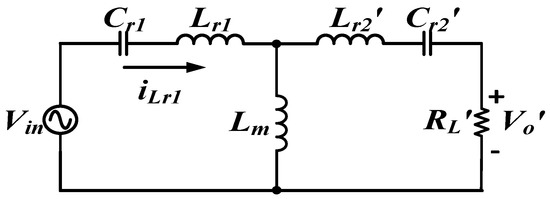
Figure 4.
Equivalent circuit of a 2C3L resonant circuit in forward energy charging mode.
Here, RL is the AC load impedance from the vehicle battery port equivalence to the transformer output side, and is the turn ratio of the DC grid port and the vehicle battery port; .
The equivalent circuit in Figure 4 was derived into a relation to solve for the voltage gain of the 2C3L resonant circuit, as expressed in Equation (1).
where
;
;
;
;
;
.
The 2C3L resonant circuit has identical forward and reverse architectures and is therefore symmetrical. Because the reverse resonant voltage gain is similar to Equation (1), only the forward gain was used as the representative in this study
3.2. Inferences about Voltage Gains with 2C2L Circuit
The analysis of the 2C2L resonant circuit forward mode was the same as that of the 2C3L resonant circuit. First, the output-side parameters of the transformer were reduced into the input side (Figure 5).
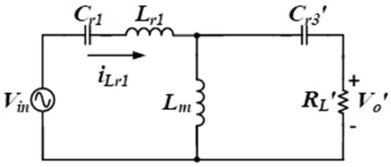
Figure 5.
Equivalent circuit of a 2C2L resonant circuit in forward energy charging mode.
Here, RL is the AC load impedance from the battery charging port equivalence to the transformer output side, and is the turn ratio of the DC grid port and the batter charging port; The equivalent circuit in Figure 5 was derived into a relation to solve for the voltage gain of the 2C2L resonant circuit, as expressed in Equation (2).
where;
;
;
;
;
;
, and . In addition, k2 and 2C3L had the same forward architecture as that of k1.
The analysis of the reverse mode of the 2C2L resonant circuit was the same as that of the forward mode; the output-side parameters of the transformer were reduced into the input side (Figure 6).
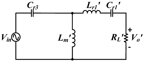
Figure 6.
Equivalent circuit of a 2C2L resonant circuit in reverse energy charging mode.
The equivalent circuit in Figure 6 was derived into a relation to solve for the reverse mode voltage gain of the 2C2L resonant circuit, as expressed in Equation (3).
where
;
;
;
;
;
;
;
;
, and .
4. Circuit Parameters and Design
This section introduces the circuit requirements and design considerations of the three-port resonant power converter. One major consideration was the resonance parameters. By following the flowchart in Figure 7, the designs steps are described in detail, and the process of selecting the resonance parameters that satisfy the power conversion requirements of the three power ports will be described.
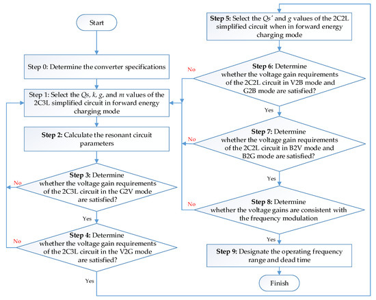
Figure 7.
Isolated three-port power converter with 2C3L and 2C2L resonant circuits.
- Step 0: Determining the converter specifications.
Considering the relevant regulations for energy storage systems and the market demand for power electronics products, the specifications for this converter system were determined. The DC grid port uses DC 400 V for energy conversion, which has a higher conversion efficiency. The vehicle battery port’s specification was based on the charging and discharging range of the electric vehicle battery pack, and was set as 280 V~403 V. The battery bank port was comprised of four standard energy storage battery modules in series, with a total voltage of 192 V; therefore, this port was set to a DC voltage range of 180 V~213 V. The design specifications of the power converter in this study are shown in Table 2. In addition, all relevant coefficients required for the subsequent design of the converter were also calculated.
Table 2.
Selected specifications of the converter.
The transformer turn ratio is calculated as follows:
The maximum and minimum gains in the six operating modes are given by Equations (6)–(17):
The equivalent impedance of the six operating modes was calculated using Equations (18)–(22). Here, the voltage of the DC grid port was 400 V; the nominal voltage of the vehicle battery port, , was 360 V; and the nominal voltage of the battery-charging port, , was 192 V. In Equations (18)–(22), , , and are the current values when the system capacity is 3 kVA.
- Step 1: Selecting the Qs, k, g, and m values of the 2C3L simplified circuit in the forward energy charging mode
- Selecting Quality Factor Q: The relation of the voltage gains of the 2C3L resonant circuit is given by Equation (1). The desired Q value cannot be easily determined using this relation. According to the literature, most studies have involved simplifying the 2C3L circuit into an LLC circuit [12,13,14,15]. The inductive reactance value of in Figure 4 is typically much greater than those of and . In particular, when the system is operating near the resonant frequency, the resonant reactance values of and decrease. As a result, the position of exciting inductance L_m shifts toward the load side. In Figure 8, exciting inductance of the 2C3L in Figure 4 shifts toward the load side, forming a new and simplified LLC circuit. However, Figure 9 and Figure 10 indicate differences between the simplified LLC resonant gain curve (Figure 9) and the 2C3L resonant gain curve (Figure 10). Figure 9 shows that there was no double peak problem for the LLC resonant circuit. However, as shown in Figure 10, for higher-order 3L2C resonant circuits, the high Q values easily result in double peaks, which cannot be detected when the Q values are low. Double peaks resulting from an overly high Q value could not be observed on the LLC gain curve. Consequently, Q values cannot be directly selected from the LLC resonant gain curve and must instead be selected from the 2C3L resonant gain curve. To simplify the design process, the quality factor of the simplified LLC circuit was designated as Q, and this Q value was used to obtain the parameters of the energy charge–discharge components and in the resonant circuit, which were designated as the benchmarks for adjusting the gain curves. By using these benchmarks, the parameters of the energy charge–discharge components and in the 2C3L resonant circuit, corresponding to the LLC gain curves under different Qs values, can be obtained. Qs is not equal to the actual quality factor of the circuit. As Figure 10 demonstrates, an overly high Qs cannot satisfy the maximum voltage gain value, and if the Qs is too small, the smallest voltage gain value cannot be satisfied either. In the end, this study used 0.4 as the Qs value. Whether this value satisfied the study requirements was determined on the basis of the design process.
 Figure 8. Simplifying the 2C3L exciting inductance position to form an LLC circuit.
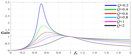 Figure 9. LLC resonant gains under different Q values.
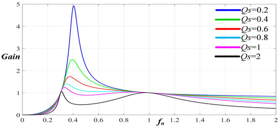 Figure 10. 2C3L resonant gains corresponding to different LLC Qs values.
 - Selecting the Value of Inductance Coefficient k: The smaller the exciting inductance , the greater the peak value of the exciting current becomes. This ensures that the parasitic capacitance energy exchange can be completed during the dead time, thereby achieving ZVS zero-voltage soft switching in the input-side power switch. As illustrated in Figure 11, the smaller the k value, the better the frequency modulation performance; however, this simultaneously augments exciting current and therefore increases the turn-off loss and conduction loss in the input-side power switch, thus decreasing the overall efficiency of the converter. In terms of soft switching and overall efficiency, increasing the k value is desirable. To satisfy the frequency modulation range, a greater k value should be selected to ensure soft switching, frequency modulation capabilities, and overall efficiency. The k value was determined as 5 in this study.
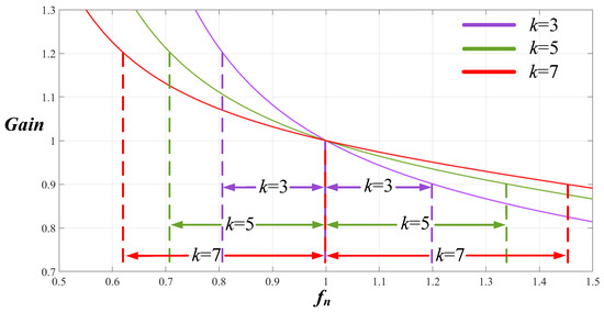 Figure 11. Effects of the k value on the frequency modulation.
 - Selecting the g Value of the Resonant Capacitance Ratio and the m Value of the Resonant Inductance Ratio: When g = m = 1 was used in the gain characteristics analysis, the output-side resonant component became the same as the input-side resonant component after it was referred to the input-side, similar to the forward and reverse gain curves within the 2C2L resonant architecture. In the 2C3L resonant framework, the gain curves were exactly the same, providing the converter with the advantages of an LLC resonant circuit in both the forward and reverse directions.
- Step 2: Calculating the resonant circuit parameters
After the value of the circuit architecture parameter Qs was selected, the resonance parameter expression was used to obtain the parameter value of each resonant component of the converter because = 1, , and ; Equations (23)–(29). In Equation (23), is the capacitance value of the series comprising and ; and can be determined using Equation (24).
The inductance value of and in a series is expressed in Equation (25); and can be determined using Equation (26).
when = 5, can be expressed using Equation (27).
- Step 3: Determining whether the voltage gain requirements of the 2C3L circuit in the G2V mode are satisfied
The 2C3L resonant voltage gain curve parameters in this study were k1 = 5, Qs = 0.4, and g1 = m1 = 1. Qs is the quality factor corresponding to the simplified LLC circuit. As demonstrated in Equations (6) and (7) and in Figure 12, this group of parameters can exist within the frequency modulation range predicted in the electrical specifications, and the gain curve can satisfy the voltage gain requirements when the operating frequency is between 100 and 200 kHz. Because of the bidirectional symmetry of the 2C3L resonant circuit, when turn ratio N, resonant capacitance ratio g, and resonant inductance ratio m are equal to 1, the forward and reverse curve characteristics are exactly the same, and during the forward and reverse operations, the target voltage gain value can be achieved by modulating the switching frequency of the power switch on the basis of the energy charge–discharge conditions. If the gain requirements of the 2C3L resonant circuit in G2V mode cannot be satisfied, then step 1 must be repeated to select the k1, Qs, g1, and m1 parameters.
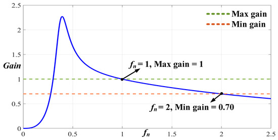
Figure 12.
Voltage gain curve of the 2C3L resonant circuit in G2V mode.
- Step 4: Determining whether the voltage gain requirements of the 2C3L circuit in the V2G mode are satisfied
Because the 2C3L resonant circuit uses the same equation for forward and reverse gains, in this mode, the voltage gain curve is the same as that in the G2V mode, and the target voltage gain value can be achieved by modulating the switching frequency of the power switch on the basis of the energy charge–discharge conditions. If the voltage gain requirements of the 2C3L resonant circuit in V2G mode are not satisfied, the parameter values must be reselected by returning to step 1. As demonstrated in Equations (8) and (9) and in Figure 13, the gain curve can satisfy the maximum and minimum voltage gains when the operating frequency is between 60 and 100 kHz.
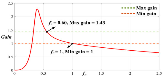
Figure 13.
Voltage gain curve of the 2C3L resonant circuit when in V2G mode.
- Step 5: Selecting the Qs′ and g values of the 2C2L simplified circuit when in the forward energy charging mode
Because this study used a triple-winding transformer, the coefficient of inductance k of the 2C2L resonant circuit was the same as that of the 2C3L resonant circuit. The 2C2L resonant architecture was nonsymmetrical and therefore had a higher degree of freedom in its design than did the 2C3L resonant circuit. Under certain specifications, the frequency operating range can be narrowed by selecting an appropriate g value; however, altering the g value affects the total value of the equivalent resonant capacitance and therefore alters the quality factor Qs of the circuit. For this reason, the g value was set to 1, as depicted in Equation (30). Compared with the 2C3L resonant circuit, the 2C2L resonant circuit reduced the resonant inductance on the output side of the transformer. Thus, given a g value of 1, the quality factor Qs′ of the exciting inductance overlooked by the 2C2L resonant circuit was 0.707 times the Qs value of the exciting inductance overlooked by the 2C3L resonant circuit, as demonstrated by Equation (31).
- Step 6: Determining whether the voltage gain requirements of the 2C2L circuit in V2B mode and G2B mode are satisfied
The parameters selected in Steps 1 and 2 were entered into the voltage gain in Equation (2). MATLAB simulation software was employed to graph the voltage gain curve and determine whether the parameters satisfied the gain requirements of the 2C2L resonant circuit in the forward modes. If not, the process must return to step 1 to select new parameter values. The inability to satisfy the maximum voltage gain is due to an overly high Qs value or k value; the inability to satisfy the minimum gain may be because the Qs value is too small or the k value is too large. Because the Qs value was adjusted first, the converter was operated near the resonance point, and the k value was increased within the designated frequency modulation range to increase the overall efficiency of the converter. Figure 14 presents the gain curve in the V2B mode; as demonstrated by Equations (10) and (11), this gain curve can satisfy the voltage gain range when the operating frequency is between 61 and 215 kHz.
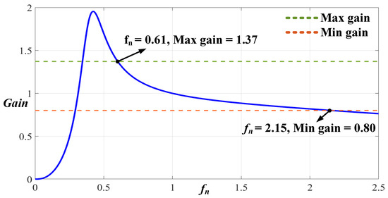
Figure 14.
Voltage gain curve of the 2C2L resonant circuit when in V2B mode.
- Step 7: Determining whether the voltage gain requirements of the 2C2L circuit in B2V mode and B2G mode are satisfied
The k, g, and m parameters in reverse mode were the same as those in forward mode after they were referred to the transformer turn ratio. Thus, the k, g, and m parameters in forward mode can be directly entered into Equation (3) and modeled using MATLAB to obtain the voltage gain curve to determine whether the 2C2L voltage gain requirements in reverse mode are met. If not, new parameter values must be selected by returning to step 1. Figure 15 demonstrates the voltage gain in B2V mode; as indicated by this example and Equations (12) and (13), this gain curve can satisfy the maximum and minimum voltage gains when the operating frequency is between 89 and 233 kHz.
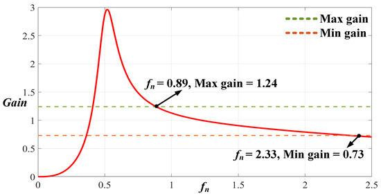
Figure 15.
Voltage gain curve of the 2C2L resonant circuit when in B2V mode.
- Step 8: Designating the operating frequency range
The voltage gain graphs demonstrate that the highest and lowest switching frequencies were 233 and 60 kHz, respectively, which are consistent with the designated frequency modulation range. ZVS dead time can be achieved at these designated frequencies.
- Step 9: Designating the operating deadtime
The power switch used in this study was a silicon carbide field-effect transistor developed by United SiC (part number UJ3C065080K3S). This transistor has a parasitic capacitance of 104 pF, enabling the circuit to achieve ZVS more readily.
The circuit includes many stray and parasitic capacitances that were not considered. To retain the margin of the dead time and prevent the power switch from being erroneously connected, the dead time was set to 200 ns.
5. Experimental Results
This study created a resonant converter that enables power conversion with a rated output of 3 kW between the three isolated ports. The system control of the circuit was a Texas Instruments TMS320F28335 microcontroller [16]. The prototype of the proposed converter is shown in Figure 16 and provides bidirectional power transfers among a DC grid port, vehicle battery port, and battery charging port. The circuit specifications are presented in Table 3. Table 4 presents a list of the actual circuit parameter settings and components that were used. To increase the efficiency of the converter, this study used a new type of wide-bandgap SiC switch in place of a conventional silicon switch. The wide-bandgap SiC switch demonstrated lower switching loss with switching at high frequencies, thereby increasing the circuit switching efficiency.
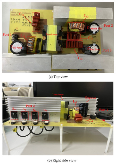
Figure 16.
The prototype of the proposed converter. (a) Top view; (b)Right side view.
Table 3.
Electrical specifications of the converter.
Table 4.
Circuit parameters and components.
5.1. Key Waveforms When Operating in G2V Energy Charging Mode
This study involved multiple operational modes. ZVS was explained solely on the basis of the transfer of power from the DC grid port to the vehicle-use battery port. G2V mode is the charging of energy in the CC–CV mode from the DC grid port to the vehicle-use battery port.
Figure 17a,b depicts the vGS4, vDS4, and iDS4 waveforms when the DC grid port was 400 V and the vehicle battery port was 280 and 403 V. Respectively, vGS4, vDS4, and iDS4 are the signal, voltage, and current of power switch on the input side. In Figure 17a, the frequency fs of the operating point was 200 kHz, and in Figure 17b, it was100 kHz, as demonstrated by the maximum and minimum gain working points in Figure 12. The figures demonstrate that the reverse current iDS4 flowed through before power switch was connected; this reverse current enabled the discharge of energy stored in the parasitic capacitance of the power switch, causing cross voltage vDS4 of the switch to drop rapidly to 0 V, thereby achieving ZVS. This also reduced the switching loss of the power switch.
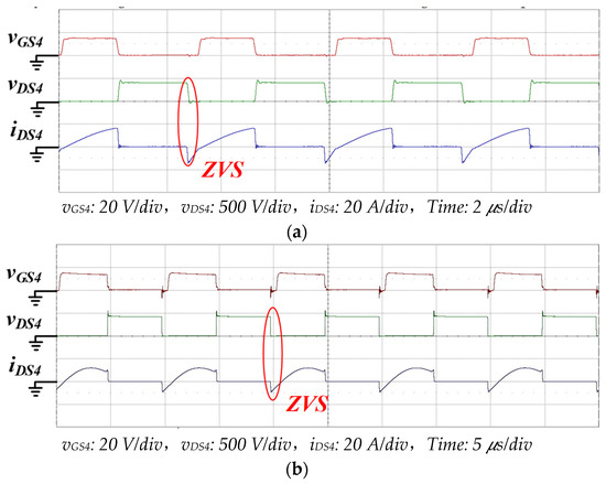
Figure 17.
The vGS4, vDS4, and iDS4 waveforms in G2V mode. (a) VDC Grid = 400 V, VVehicle_Bat = 280 V, IVehicle_Bat = 7.5 A; (b) VDC Grid = 400 V, VVehicle_Bat = 403 V, IVehicle_Bat = 7.5 A.
Figure 18a,b depicts the vDS8 and iDS8 waveforms when the DC grid port was 400 V and the vehicle battery port was 280 and 403 V. Respectively, vDS8 and iDS8 are the voltage and current of power switch on the input side. As depicted in Figure 12, the frequency of the operating point in Figure 18a was 200 kHz; when the converter was working in Region I, because iDS8 had not yet reduced the current to 0 A before the increase in vDS8, the ZVS function on the output-side power switch was lost, increasing the switching loss. As depicted in Figure 12, the frequency of the operating point in Figure 18b was 100 kHz; when the converter was working in Region II, the decoupling region did not have energy to be transferred to the output, and consequently, the diode on the output side naturally cut off, thereby ensuring flexible ZCS.
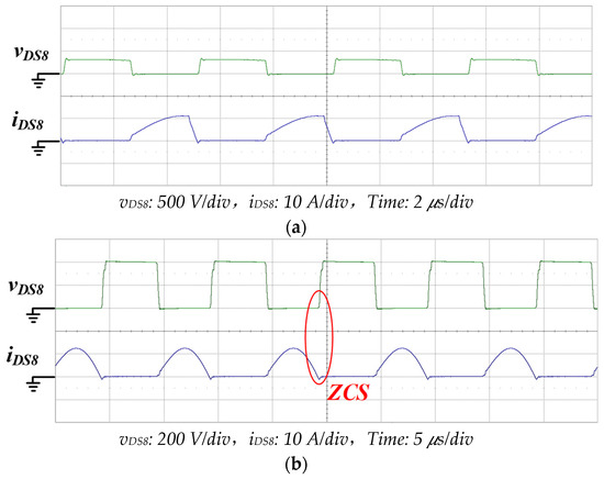
Figure 18.
The vDS8 and iDS8 waveforms in G2V mode. (a) VDC Grid = 400 V, VVehicle_Bat = 280 V, IVehicle_Bat = 7.5 A; (b) VDC Grid = 400 V, VVehicle_Bat = 403 V, IVehicle_Bat = 7.5 A.
5.2. Efficiency of Six Operating Modes
Figure 19 depicts the bidirectional power conversions of 3 kW among the DC grid port (400 V), vehicle battery port (280–403 V), and battery charging port (180–213 V) in six operational modes. As demonstrated in Figure 12 and Figure 13, G2V and V2G are the 2C3L forward and reverse modes. In Figure 13, the V2G mode involved operations in Region II and exhibited ZVS and ZCS. Compared with the G2V mode in Figure 12, which only occurred in Region I, the V2G mode exhibited a higher conversion efficiency, as high as 96.9%. G2B and V2B were the 2C2L forward modes, with conversion efficiencies as high as 93.77% and 93.87%, respectively. The V2B mode was more efficient than the G2B mode. B2G and B2V were the 2C2L reverse modes and had the lowest converter efficiencies, which were 93.26% and 92.68% at most, respectively. Because the voltage of the DC grid port was higher than the nominal voltage of the vehicle battery, the B2G efficiency was slightly higher than the B2V efficiency. Among the six operating modes depicted in Figure 19, when the 2C3L converter capacity was 3 kVA, the G2V and V2G modes exhibited slightly higher efficiencies than the 2C2L operations in the B2G, G2B, V2B, and B2V modes. This may be because of the lower voltage of the system’s battery charging port, which decreased the efficiency by creating higher operating currents and greater conduction losses.
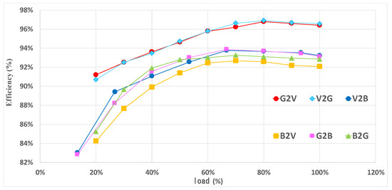
Figure 19.
Efficiencies of the six operating modes.
6. Conclusions
This study proposed an isolated three-port bidirectional resonant converter that can be applied to power dispatching. The converter improves on the bidirectional power dispatch capabilities of conventional three-port converters by adding resonant components on each side of the transformer, enabling the energy charge–discharge through ports of different voltage levels through the use of different resonant converters. By modulating the frequency, bidirectional power regulation and electrical isolation were achieved among the three ports with different voltage levels. Because of its favorable resonance characteristics, the converter demonstrated soft switching when encountering a wide range of changes to the load, thereby reducing the power loss during the switching process and increasing the overall efficiency and stability of the converter. A triple-winding transformer is the core of the design. The proposed design eliminates the need to handle energy transmission among the three ports through three separate DC–DC bidirectional converters, which compels the system to include multiple converters, increasing the bulk and cost. The 2C3L and 2C2L resonant converters were demonstrated to be applicable to bidirectional power conversions. The resonant converters can be combined into a three-port power converter wound around a single transformer core.
Renewable energy is becoming more and more widespread. In the future, a new port for solar power generation will be added to the original architecture in this research to form a multi-port converter, allowing solar energy to be supplied to the DC grid port, the car battery port, and the battery storage port. Additionally, voltage and temperature changes cause instability in various switching components, and sudden changes in load during charging and discharging lead to system instability [17,18], so the stability control mechanism of the converter is also a very important research topic.
Author Contributions
Conceptualization, Y.-N.C. and Y.-H.Y.; methodology, Y.-N.C.; software, Y.-H.Y. and S.-M.H.; writing—original draft preparation, S.-M.H. and Y.-H.Y.; writing—review and editing, Y.-H.Y. and Y.-N.C. All authors have read and agreed to the published version of the manuscript.
Funding
This research received no external funding.
Conflicts of Interest
The authors declare no conflict of interest.
References
- Foti, S.; Testa, A.; Scelba, G.; De Caro, S.; Tornello, L.D. A V2G Integrated Battery Charger Based on an Open End Winding Multilevel Configuration. IEEE Open J. Ind. Appl. 2020, 1, 216–226. [Google Scholar] [CrossRef]
- Wang, S.; Li, H.; Zhang, Z.; Li, M.; Zhang, J.; Ren, X.; Chen, Q. Multifunction Capability of SiC Bidirectional Portable Chargers for Electric Vehicles. IEEE J. Emerg. Sel. Top. Power Electron. 2021, 9, 6184–6195. [Google Scholar] [CrossRef]
- Pérez, P.; Veirano, F.; Silveira, F. A Compact Lithium-Ion Battery Charger for Low-Power Applications. IEEE Trans. Circuits Syst. II Express Briefs 2022, 69, 669–673. [Google Scholar] [CrossRef]
- Dinh, H.T.; Yun, J.; Kim, D.M.; Lee, K.-H.; Kim, D. A Home Energy Management System with Renewable Energy and Energy Storage Utilizing Main Grid and Electricity Selling. IEEE Access 2020, 8, 49436–49450. [Google Scholar] [CrossRef]
- Lee, S.; Choi, D.-H. Federated Reinforcement Learning for Energy Management of Multiple Smart Homes with Distributed Energy Resources. IEEE Trans. Ind. Inform. 2022, 18, 488–497. [Google Scholar] [CrossRef]
- Aznavi, S.; Fajri, P.; Asrari, A.; Harirchi, F. Realistic and Intelligent Management of Connected Storage Devices in Future Smart Homes Considering Energy Price Tag. IEEE Trans. Ind. Appl. 2020, 56, 1679–1689. [Google Scholar] [CrossRef]
- Shah, S.S.; Rastogi, S.K.; Bhattacharya, S. Paralleling of LLC Resonant Converters. IEEE Trans. Power Electron. 2021, 36, 6276–6287. [Google Scholar] [CrossRef]
- Tang, X.; Wu, H.; Hua, W.; Yu, Z.; Xing, Y. Three-Port Bidirectional Series-Resonant Converter with First-Harmonic-Synchronized PWM. IEEE J. Emerg. Sel. Top. Power Electron. 2021, 9, 1410–1419. [Google Scholar] [CrossRef]
- Tran, Y.; Freijedo, F.D.; Dujic, D. Open-loop power sharing characteristic of a three-port resonant LLC converter. CPSS Trans. Power Electron. Appl. 2019, 4, 171–179. [Google Scholar] [CrossRef]
- Yan, X.; Liu, C.; Liu, S.; Guo, X.; Zou, X. An Improved Interleaved Buck/Boost Integrated CLLLC Three-Port DC-DC Converter for Wide Input Range. In Proceedings of the 2021 IEEE 2nd China International Youth Conference on Electrical Engineering (CIYCEE), Chengdu, China, 15–17 December 2021; pp. 1–7. [Google Scholar]
- Wang, C.; Li, W.; Wang, Y.; Han, F.; Meng, Z.; Li, G. An Isolated Three-Port Bidirectional DC-DC Converter with Enlarged ZVS Region for HESS Applications in DC Microgrids. Energies 2017, 10, 446. [Google Scholar] [CrossRef]
- Huang, J.; Liang, T.; Tseng, W.; Chen, Z. Design and Implementation of Three-Level Half-Bridge Bidirectional CL3C Resonant DC Converter. In Proceedings of the 2019 IEEE Energy Conversion Congress and Exposition (ECCE), Baltimore, MD, USA, 29 September–3 October 2019. [Google Scholar]
- Zahid, Z.U.; Dalala, Z.M.; Chen, R.; Chen, B.; Lai, J. Design of Bidirectional DC–DC Resonant Converter for Vehicle-to-Grid (V2G) Applications. IEEE Trans. Transp. Electrif. 2015, 1, 232–244. [Google Scholar] [CrossRef]
- Xie, H.; He, Y.; Hang, L.; Zeng, P.; Zhan, X. Research on Improved Modeling Method of CLLLC Resonant Converter. In Proceedings of the 2022 IEEE International Power Electronics and Application Conference and Exposition (PEAC), Guangzhou, China, 4–7 November 2022; pp. 1642–1648. [Google Scholar]
- Zong, S.; Fan, G.; Yang, X. Double Voltage Rectification Modulation for Bidirectional DC/DC Resonant Converters for Wide Voltage Range Operation. IEEE Trans. Power Electron. 2019, 34, 6510–6521. [Google Scholar] [CrossRef]
- Mouser Electronics. Available online: https://www.mouser.tw/datasheet/2/827/DS_UJ3C065080K3S-1530409.pdf (accessed on 9 January 2023).
- Stathis, J.H.; Zafar, S. The negative bias temperature instability in MOS devices: A review. Microelectron. Reliab. 2006, 46, 270–286. [Google Scholar] [CrossRef]
- Schmidt, S.; Oberrath, J.; Mercorelli, P. A Sensor Fault Detection Scheme as a Functional Safety Feature for DC-DC Converters. Sensors 2021, 21, 6516. [Google Scholar] [CrossRef]


Disclaimer/Publisher’s Note: The statements, opinions and data contained in all publications are solely those of the individual author(s) and contributor(s) and not of MDPI and/or the editor(s). MDPI and/or the editor(s) disclaim responsibility for any injury to people or property resulting from any ideas, methods, instructions or products referred to in the content. |
© 2023 by the authors. Licensee MDPI, Basel, Switzerland. This article is an open access article distributed under the terms and conditions of the Creative Commons Attribution (CC BY) license (https://creativecommons.org/licenses/by/4.0/).