Article

PLF Design for DC-DC Converters Based on Accurate IL Estimations

by
Marco Bosi
1,2,
Albert-Miquel Sánchez
3,
Francisco Javier Pajares
3,
Alessandro Campanini
2 and
Lorenzo Peretto
2,*
1
Wavecontrol SL, Carrer de Pallars 65, 08014 Barcelona, Spain
2
Department of Electrical, Electronic and Information Engineering, Guglielmo Marconi Alma Mater Studiorum, University of Bologna, Viale del Risorgimento 2, 40136 Bologna, Italy
3
EMZER Technological Solutions SL, Carrer de Pallars 65, 08014 Barcelona, Spain
*
Author to whom correspondence should be addressed.
Energies 2023, 16(5), 2085; https://doi.org/10.3390/en16052085
Submission received: 12 January 2023 / Revised: 17 February 2023 / Accepted: 18 February 2023 / Published: 21 February 2023

Abstract

:
Even though today’s electromagnetic compatibility (EMC) standards and measurement techniques set specific limitations and a clear methodology to measure the conducted emissions (CE) of equipment under tests (EUTs), the design methodology of a suitable power-line filter (PLF) to solve non-compliance is, in general, neither accurate nor efficient. This is due to different reasons, such as unknown actual load and line impedances, unknown dominant mode in the CE, and/or inappropriate instrumentation for the appropriate measurements. The objective of this paper is to investigate if different topologies of switching mode power supplies (SMPSs) lead to different PLF structures. For the sake of exemplification, the analysis is focused on switched-mode DC-DC converters. From an EMC point of view, these devices can be completely modeled by means of Scattering (S)–parameter and CE measurements. Additionally, an analysis of their circuit models has been performed to allow a better comprehension of their characterization. In this paper, the circuit models of three different types of DC-DC converters are presented, and their component values (including nonlinearities and parasitic effects introduced by the actual behavior of the circuit elements) are estimated using the S-parameter characterization. Then, a new methodology for PLF design, based on accurate insertion loss (IL) estimations, is applied to obtain the optimal PLF for one of the converters. This methodology is experimentally tested and validated.

1. Introduction

International standards set specific limits and methodology for conducted emissions (CE) levels [1,2]. The measurement methodology involves the use of an Artificial Network (AN) inserted between the power source and the equipment under test (EUT), which present a known power source impedance to the EUTs. The most common way to reduce the CE of equipment under test (EUT) that does not meet the requirements of the standard is by adding a power line filter (PLF) between the power-line network (PLN) and the EUT [3,4,5,6,7,8,9,10].
A common strategy to select a suitable PLF involves relying on its insertion loss (IL), a figure of merit provided by manufacturers. It is stated in CISPR 17 [11], Annex C, that the IL of PLFs can be measured with 50-Ω impedances at their input and output ports or, to evaluate a worst-case scenario, with 0.1-Ω and 100-Ω impedances at their input and output ports respectively, and vice versa. However, actual EUTs and PLNs present complex input impedances very different from the aforementioned values, which vary with the frequency (in most cases, from a very high magnitude value to a very low one due to the parasitic effects and/or to the electrical component behaviors). Therefore, it is not possible to accurately estimate the real IL of a PLF when connected between them [7,8,9,10]. Furthermore, it has been demonstrated that an impedance mismatch in the EUT, in the PLN, or in the same PLF leads to an unexpected energy exchange between common-mode (CM) and differential-mode (DM) noise, modifying the PLF performance and results in unexpected values of CE levels [6,7,8,9,10]. Finally, commercial PLFs present static structures to mitigate both CM and DM interference (almost all PLFs contain, at least, an X-type capacitor at the line side, a CM choke, and two Y-type capacitors at the load side), and some of these components may not be strictly necessary or may not be placed in their optimal position for a specific EUT. Therefore, an oversized PLF is usually used to obtain the same mitigation that an optimal but much smaller PLF could achieve [10].
The other way to obtain an appropriate PLF is by designing it. This problem has been extensively discussed in the literature with different approaches and methodologies [3,4,5,6,7,8,9,10,11,12,13,14,15,16,17,18,19,20,21,22,23,24,25,26,27,28,29,30,31,32,33,34]. Accordingly, most EMC designers have developed their own modus operandi based on their experience, knowledge, and available instrumentation. In most cases, it ends up being a trial-and-error process since, again, there is a lack of information regarding the actual impedance of the EUT and the PLN, essential information to obtain an optimal result.
Hence, it seems that measuring the impedance of EUTs and PLNs should solve both problems stated above, but although this is something that can be done [7,8], it is tricky, and specific instrumentation, not always available (such as a two-port line impedance stabilization network (LISN)), is needed.
In this paper, in order to make the PLF design easier, the input impedances of different topologies of switched-mode power supplies (SMPSs), the most common electronic circuit found at the power-line terminals of electric and electronic devices, have been analyzed. The aim of this analysis is to check if different topologies of EUTs need different structures of PLF for optimal CE mitigation (that is, different order of components within the PLF). If that were the case, the relationship between the EUT topology and the PLF structure could be established, making the design of the optimal PLF much easier for EMC engineers.
To this end, the Scattering (S) parameters of different topologies of DC-DC converters (which are a type of SMPS) connected to a power source, which include a Buck converter, a Boost converter, and a single-ended primary-inductor converter (SEPIC), have been measured switched on. From these measurements, the circuital models of each topology, along with their parasitic components, have been extracted [35,36,37,38]. Special care has been taken to model the component parasitic effects, circuit layouts, and couplings since they all strongly affect the behavior of the input impedance [37,38]. Working with equivalent circuits instead of the measured S-parameter matrix allows a better comprehension of the SMPS input impedance and the CE phenomena while this information is scattered within the S-parameter matrix. Then, a PLF design methodology, based on an accurate IL estimation of the PLF for the CM and DM CE, developed and described in this paper, has been applied to find the optimal PLF structure for one of the DC-DC converters. The results obtained show that the work presented in this paper is useful to reduce the cost and the time duration for the optimum PLF selection or design since it provides the optimal PLF structure for three specific DC-DC converters and the methodology to find the optimal PLF for any other kind of SMPS.
This paper is organized as follows: Section 2 describes the models used to characterize the three SMPSs and which considerations have been taken into account. Section 3 reviews the measurement setups needed to obtain a complete characterization of an SMPS. Section 4 introduces the PLF design methodology. In Section 5, three actual DC-DC converters are modeled and analyzed, and the optimal PLF structure is designed, implemented, and tested. Finally, Section 6 summarizes a final discussion of the work.

2. Circuit Models of the SMPSs

This section illustrates the circuital models of three SMPSs.

2.1. Model of Buck Converter

A Buck converter, also known as a step-down converter or step-down chopper, is a DC-to-DC power converter designed to perform a step-down conversion of the input signal and typically operates with a switching frequency between 100 kHz and a few MHz. The model that describes the behavior of a real Buck converter [35,36,37,38], with parasitic and non-ideal components, is seen in Figure 1.
The inductor L, the controlled switch S, the capacitor C, and the diode D are the main components of the circuit. The load, in this case, is considered purely resistive and represented by a resistance RL (since the DC-DC converter is evaluated alone). The rest of the components are the nonlinearities and parasitic effects introduced by the actual behavior of the circuit elements [35,36,37,38]. The parameters rL, rC, rS, and rD describe the equivalent series resistances of every component, and the Lpar1 and Lpar2 represent the parasitic inductance of the PLN. Finally, the capacitor CPAR represents the stray capacitance towards ground.
The two modes of operation of the Buck converter are described below:
-
Mode 1: The switch S conducts, and the diode D is blocked. The inductor L produces an opposing voltage across its terminals in response to the changing current. This voltage drop counteracts the voltage of the source and therefore reduces the net voltage across the load;
-
Mode 2: The switch S is blocked, and the diode D conducts. The inductor becomes a current source (the stored energy in the inductor’s magnetic field supports the current flow through the load).

2.2. Model of Boost Converter

A boost converter is sometimes called a step-up converter since it “steps up” the source voltage. The equivalent circuit of a real Boost converter is shown in Figure 2.
The same ideal and parasitic components as in the case of the Buck converter are considered.
The two modes of operation of the Boost converter are described below:
-
Mode 1: The switch S conducts, and the diode D is blocked. The current is diverted through to the MOSFET through the inductor;
-
Mode 2: The switch S is blocked, and the diode D conducts. The output capacitor is charged to the sum of the input voltage and the inductor voltage, stepping up the input DC voltage to higher output.

2.3. Model of a SEPIC Converter

A SEPIC is essentially a boost converter followed by an inverted buck-boost converter. Therefore, it is similar to a traditional buck-boost converter but with some advantages due to its non-inverted output (the output has the same electrical polarity as the input). Figure 3 shows its equivalent circuit.
The two modes of operation of the SEPIC converter are described below:
-
Mode 1: The switch S conducts, and the diode D is blocked. The energy in L1 is increased, and the capacitor C1 transfers energy to the inductor L2. Since the diode D is blocked, the load’s energy comes from the capacitor C2;
-
Mode 2: The switch S is blocked, and the diode D conducts. The inductors L1 and L2 are discharged and provide energy to the load and to the capacitors C1 and C2.

3. EUT Characterization

In order to characterize a EUT (which includes the converters described above) connected to the PLN, to the LISN, or to any other kind of power network, two measurements are needed: S-parameters and CE [7,8,9,10]. To facilitate the measurements, SMA connectors have been added to the LISN-EUT interface ports and the wires of the DC-DC converters so they can be easily connected. The SMA connectors of the LISN-EUT interface are grounded to the RF ground of the LISN.
S-parameters can be measured using the setup described in Figure 4a, which basically consists of a vector network analyzer (VNA) and a LISN [7,9]. As described in CISPR 16-2-1 [39], the LISN, needed to isolate the impedance present at the power-line ports, is bonded to a reference conducting surface by means of its grounding bar placed on the rear panel. The reference conducting surface is additionally connected to the ground of the electric power distribution system. The VNA is calibrated at the LISN–EUT interface (at the ‘+’ and ‘−’ terminals of the EUT) using a standard through-open-short-match (TOSM) calibration method to compensate the effects of the LISN, the transient limiters, and the cables (in this particular case, a commercial 50-Ω SMA calibration kit was used). Finally, to obtain a correct S-parameter measurement, the power of the interference generated by the EUT has to be negligible in front of the power delivered by the VNA.
The setup used to measure the CE at the terminals of the EUT (Figure 4b) consists of a two-port EMI receiver (for instance, an EMSCOPE, an EMI receiver manufactured by EMZER, which includes a LISN [40]). The two-port EMI receiver provides direct information about the CM and DM CE, obtaining a complete representation of the EUT. Besides, this instrument automatically compensates for the effect of the LISN, the transient limiters, and the cables, making the measurement easier and faster.
With both measurements, a complete characterization of the EUT is obtained from the EMC point of view and can be used in a circuit simulator to estimate the actual IL of a PLF. Besides, S-parameters can also be used to find the component values of the circuit models presented in Section 2.

4. PLF Design

The main problem in evaluating the effectiveness of a PLF is that its actual IL cannot be estimated if line and load impedances are not known (which, for sure, will be different from 50 Ω). However, if the EUT impedance is characterized (using, for instance, the measurement setup described in Section 3), and the PLN impedance is known (in EMC measurements, the PLN impedance is always provided by the LISN, which internal circuitry is known), the actual IL of any PLF can be estimated using a circuit simulator or resolving the circuit equations using a programming computing platform. In this section, the method to estimate the actual IL of a PLF is described and latterly used to implement the optimal PLF.

4.1. Accurate Estimation of the IL of a PLF

Figure 5 shows the equivalent circuit of the EUT connected to the equivalent circuit of a LISN according to CISPR 16. The impedance of the EUT is represented with the measured S-parameters. The two voltage noise sources, Vn+ and Vn−, are added to provide a fixed amplitude signal at all frequencies, which will be used to compute the accurate IL of the PLF (since the actual impedances of the EUT and the PLN are used instead of the usual 50-Ω, 0.1-Ω, and 100-Ω measurements). CM or DM-conducted emissions can be emulated by switching the Vn− phase from 0° to 180°. The impedance of the LISN is represented by its internal circuit.
This is one among other different representations since the EUT could be modeled using the equivalent circuits shown in Section 2, and the LISN could be modeled using the measured S-parameters, but the same idea remains.
In any case, the IL of the PLF for one of the lines can be obtained with
I L d B + = 20 l o g 10 V r e f + V + ,
and, for the other line
I L d B = 20 l o g 10 V r e f V ,
where V r e f + and V r e f are the voltage at the ‘+’ and ‘−’ terminals of the LISN, respectively (or line and neutral in an AC system) when the signal is unfiltered (as seen in Figure 5, the measurement point is placed between the 0.25 μF capacitors and the 50-Ω resistors), and V + and V are the voltage at the ‘+’ and ‘−’ terminals of the LISN, respectively, when the signal is filtered (as seen in Figure 6).
The relationship between the voltage at the ‘+’ and ‘−’ terminals and the modal voltages is [7]
V C M = V + + V 2 ;   V D M = V + V .
Accordingly,
V C M r e f = V r e f + + V r e f 2 ;   V D M r e f = V r e f + V r e f .
Therefore, the actual modal IL of any PLF can be obtained with
C M   I L d B = 20 l o g 10 V C M r e f V C M = 20 l o g 10 V r e f + + V r e f V + + V ;
D M   I L d B = 20 l o g 10 V D M r e f V D M = 20 l o g 10 V r e f + V r e f V + V .

4.2. PLF Design Methodology

The simplest structure of a PLF contains one or two X-type capacitors ( C X ) between line and neutral, usually located on the sides of the CM choke, to mitigate the DM, and a CM choke (with an inductance L ) and two Y-type capacitors ( C Y ) from line to ground and neutral to ground, usually placed on the load side, to mitigate the CM (Figure 7). A resistor ( R 1 ) is usually added to discharge the capacitors when the voltage is disconnected.
However, the PLF structure shown in Figure 7 may not be optimal for a specific EUT. Nevertheless, using the PLF modal IL estimation described above, different structures can be easily added and tested to find the optimal one. Therefore, the methodology to design the optimal PLF consists of the following steps:
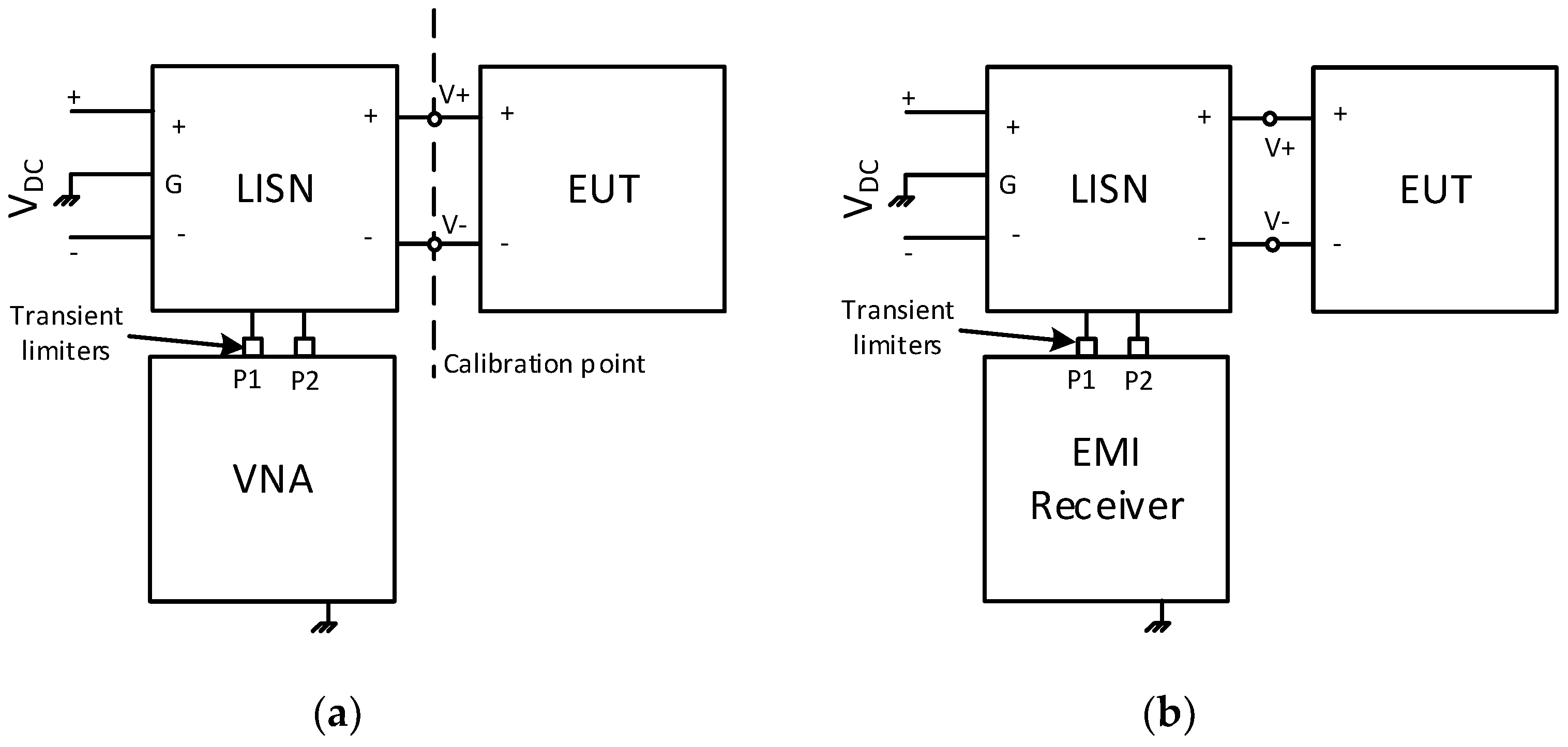
  • Measurement of the S-parameters of the EUT;
  • Measurement of the modal CE and determination of the IL needed to mitigate each mode under a threshold level;
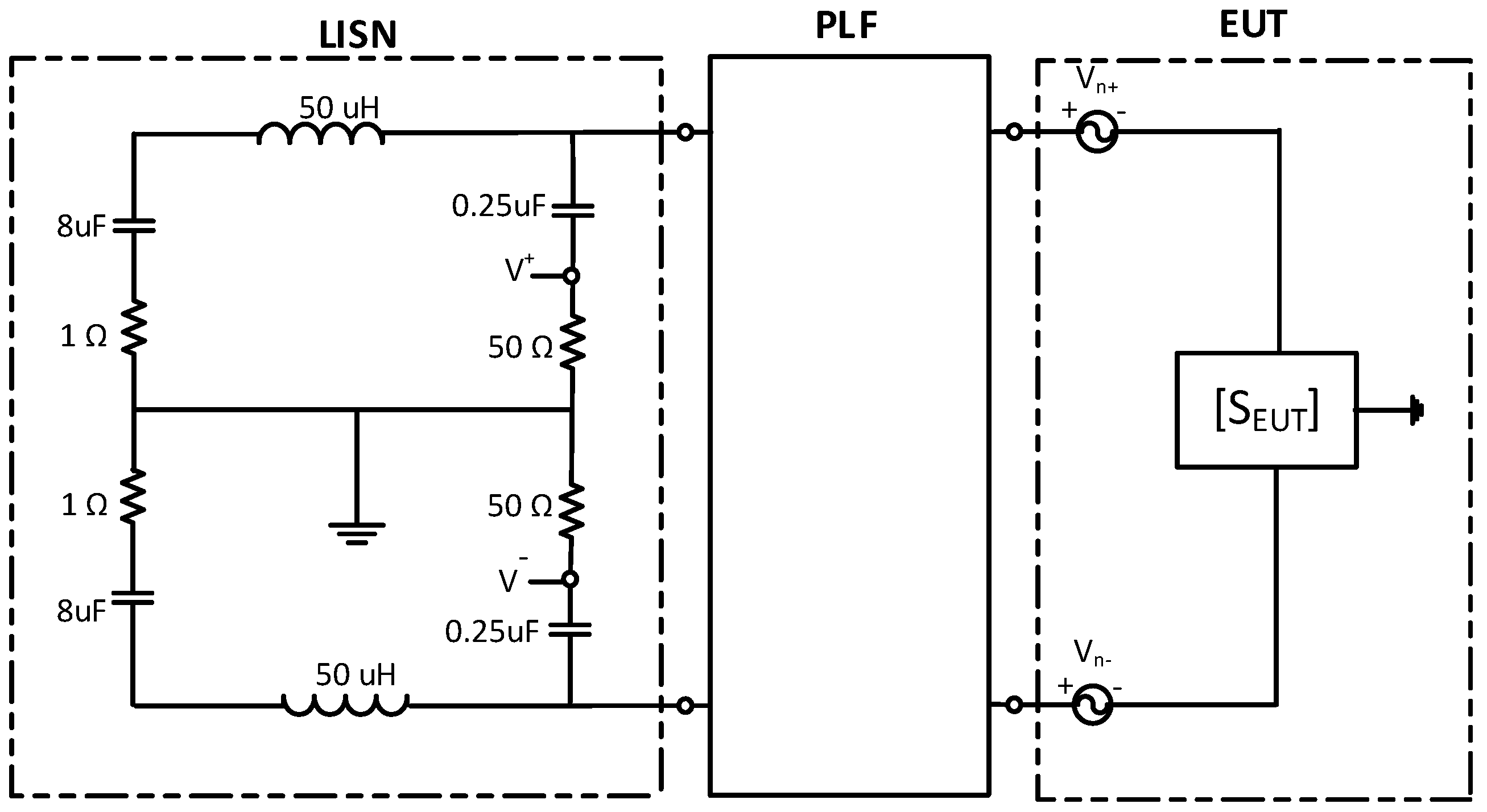
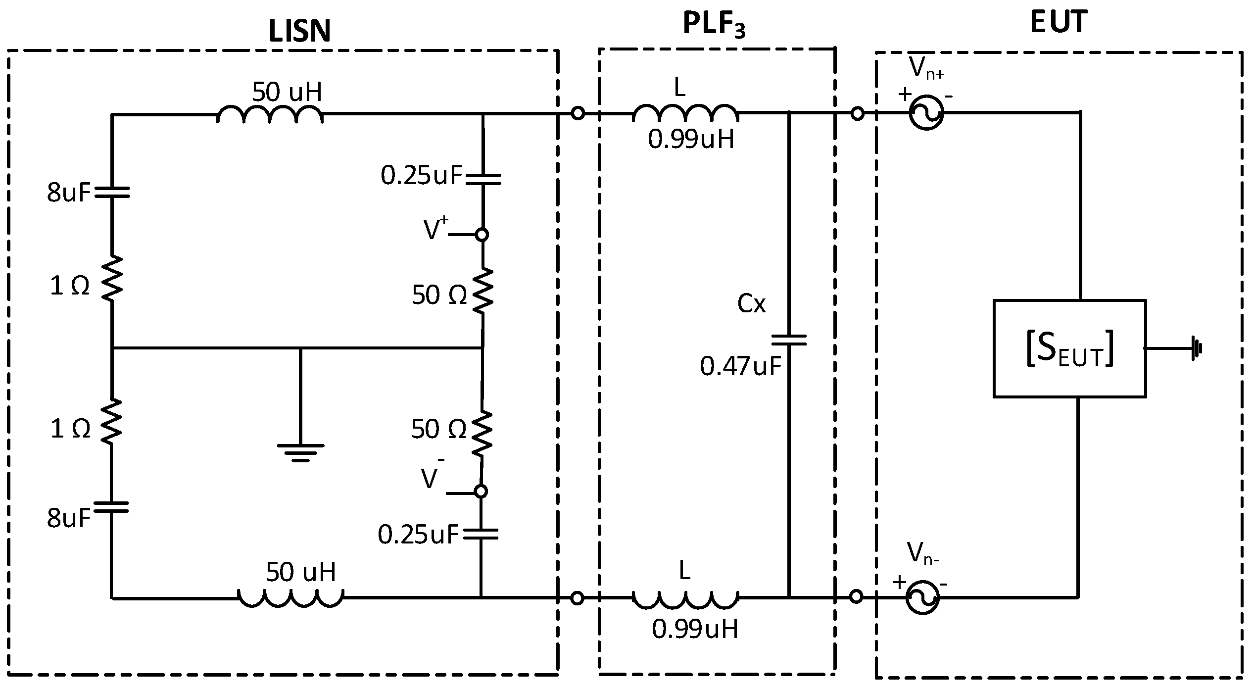
  • Introduction of the S-parameters in a circuit simulator as a black box with two ports. The circuit is completed by adding two voltage sources and a LISN circuit, as seen in Figure 5. The two voltage sources emit the same amplitude at all frequencies, and their phase can be modified between 0° and 180° to have pure CM or DM CE, respectively;
  • The same circuit is implemented again in the simulator adding the PLF, as seen in Figure 6;
  • Both circuits are simulated in the frequency domain, obtaining the voltage amplitude at the measurement ports of the LISN in both cases (that is, V r e f + ,   V r e f , V + , V ). The CM IL is computed using (5), and the DM IL using (6) (they are both introduced in the simulator, which provides the result);
  • Since each simulation needs less than a second to be completed, the determination of the optimal values for each PLF component and its optimal position inside the PLF is done manually using iterative simulations. Optionally, optimization techniques can be implemented to improve this methodology.

5. Experimental Validation

In this section, the three models of the converters are validated using S-parameter measurements. These equivalent circuits make understanding the input impedance and the CE phenomena easier since this information is scattered within the S-parameter matrix. Then, the CE of one of the converters is measured, and its optimal PLF is designed.

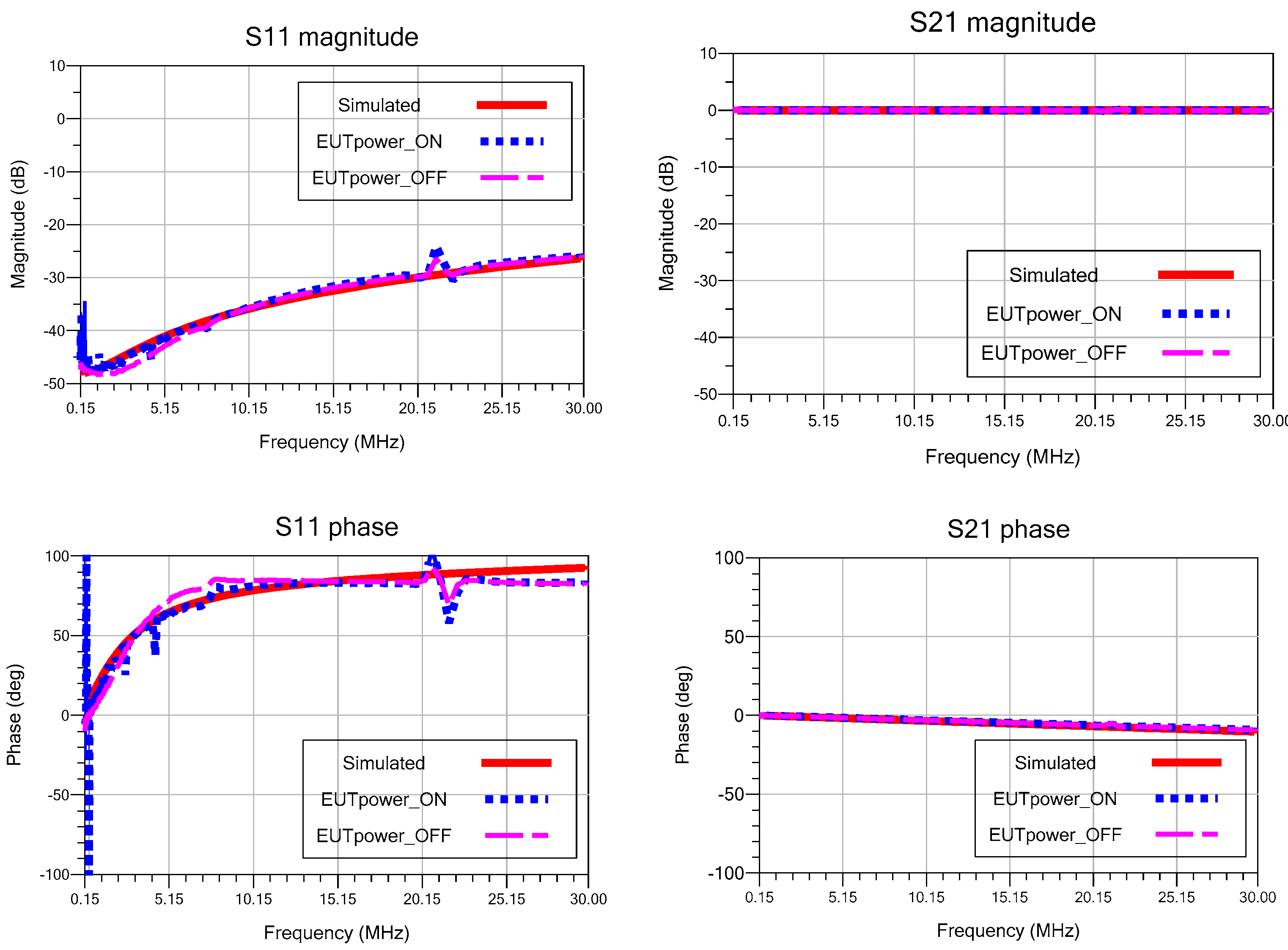
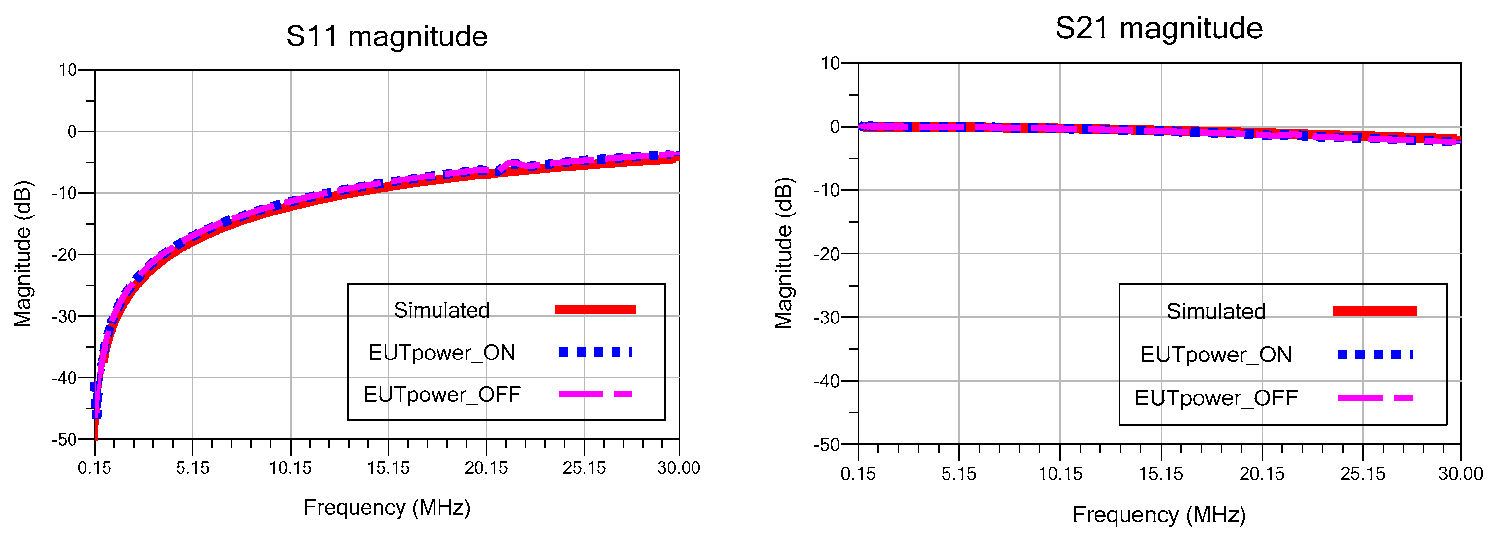
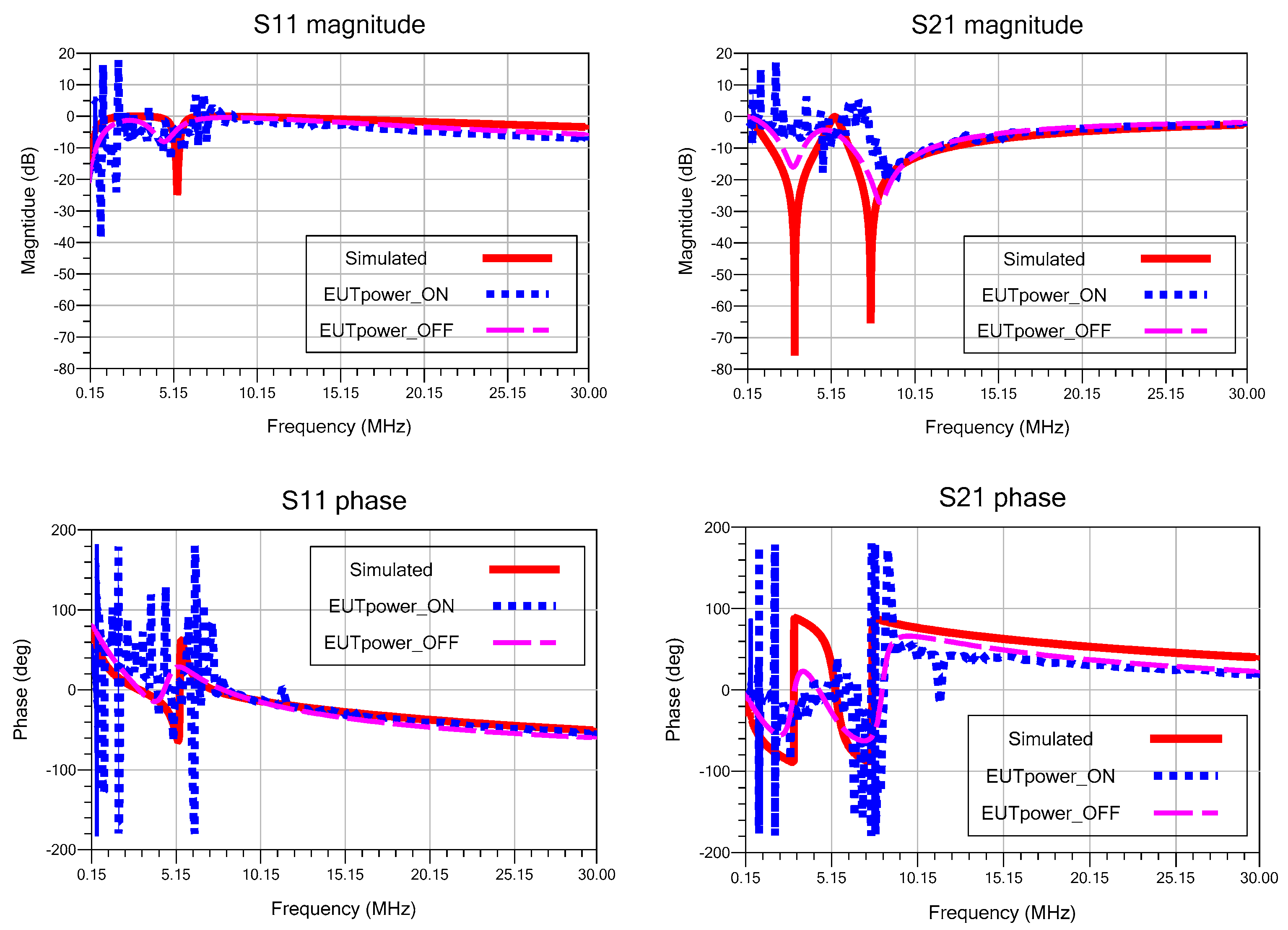
5.1. Validation of the Circuit Models

In order to validate the three models of the converters described in Section 2, the S-parameter matrix of the three converters has been measured using the setup described in Section 3, Figure 4a. The load impedances connected to the DC-DC converters were known (preliminary measurements of the DC-DC converters were done using different load conditions, and, for each converter, the ones that provided the worst conditions, that is, the ones that caused the higher values in their conducted emissions, were selected). An actual picture of this same setup is shown in Figure 8.
In order to find the values of the parasitic components, the following procedure has been followed:
  • The circuit model is implemented in a circuit simulator using the values provided in the datasheet for the normal components (CIN, D, C, …). Parasitic components (CPAR, Lpar1, Lpar2, rS, rD, rC, rL, …) are added with a ‘0’ value. For each parasitic component, a margin of possible values is considered in the simulator;
  • The S-parameter measurements obtained from the actual EUT are also introduced in the circuit simulator;
  • An optimization algorithm, based on the gradient search method, modifies the values of the parasitic components (within the specified margin) until the computed S-parameters of the circuit model are as equal as possible to the measured ones. When the results are satisfactory (that means that measured and computed S-parameters are very similar both in phase and amplitude), the values of the parasitic components are updated with the values found in the last iteration of the algorithm.
The results obtained are shown below.

5.1.1. Circuit Validation of the DC-DC Buck Converter Power Supply Module Output 1.23 V–30 V, Model LM2596

Table 1 shows the values of the parasitic components obtained for the Buck converter model shown in Figure 1.
A few considerations should be added. Lpar1 and Lpar2 are placed before CIN, and they play an important role in the circuit. The difference between the obtained values of Lpar1 and Lpar2 is due to the difference in the wire length used for the measurements. Although they do not significantly affect the computed amplitude of the S-parameters, these values influence their phase. On the other hand, although the capacitor impedance is small, its value is frequency dependent. At lower frequencies, its impedance is higher; therefore, the rest of the circuit is less isolated. The parasitic values obtained for CPAR, rS, rD, rC, and rL, may not be as precise as Lpar1 and Lpar2, but their combination in the circuit model helps to introduce the same effect as the actual circuit does after CIN.
Figure 9 shows the comparison between the measured S-parameters and the computed ones using the circuit component values shown in Table 1 (to simplify the comparison, only the magnitude and the phase of the parameters S 11 and S 12 are shown since S 11 S 22 and S 12 S 21 ).
S-parameters were measured with the EUT switched on first and with the EUT switched off latterly. As can be seen in Figure 9, both measurements are similar. Looking at the circuit model of Figure 1, this behavior can be expected since the small impedance introduced by the input capacitor CIN at the frequencies of interest isolates the rest of the circuit. This capacitor does not usually appear in an ideal representation of a Buck converter, but it is always used since it stabilizes the input voltage and mitigates the CE (a measurement without this capacitor is shown latterly for the SEPIC converter case as an example).
Regarding the circuit model, two simulations were done to emulate the switching behavior of the MOSFET and the diode. First, with the MOSFET active and the diode inactive, and second, the other way around. In both cases, active values were represented with a small resistance (200 mΩ) and inactive values with a high resistance (5 mΩ). However, the S-parameters obtained in both cases were identical, and the reason behind this is, again, the effect due to the small impedance introduced by the input capacitor CIN. Therefore, only the first simulation (MOSFET active and diode inactive) is shown in Figure 9.
In any case, a good agreement is obtained when comparing both measurements with the simulation of the circuit model after updating the component values.

5.1.2. Circuit Validation of the Boost Converter Model MCP1640EV-SBC

Table 2 shows the values of the parasitic components obtained for the Boost converter model shown in Figure 2.
Figure 10 shows the comparison between the measured S-parameters and the computed ones with the resulting circuit. The same considerations described for the Buck converter apply here. A good agreement is obtained between measurement and simulation, validating the circuit model of Figure 2.

5.1.3. Circuit Validation of the DC-DC SEPIC Converter Model MCP1663

Table 3 shows the values of the parasitic components obtained for the Buck converter model shown in Figure 3.
Figure 11 shows the comparison between the measured S-parameters and the computed ones with the resulting circuit, obtaining, again, a very good agreement, although small differences are observed for the two phase plots at lower frequencies.
In order to show the effect of the input capacitor CIN on the circuit, an additional measurement was done for this particular converter with the capacitor removed. Measurement and simulation results to show how S-parameter measurements are affected by the increment of the CE levels are shown in Figure 12. At those frequencies where the CE levels are close to or above the levels of the transmitted and reflected waves of the VNA (which has already been configured to supply its maximum output power), the S-parameters become significantly inaccurate and useless. This measurement justifies the necessity of the capacitor CIN from an EMC point of view since it reduces the CE and, therefore, improves the EUT characterization via S-parameter measurements.
Since the three converters present a similar input impedance (due to CIN), the following analysis (CE and PLF design) has only been applied to one of the converters.

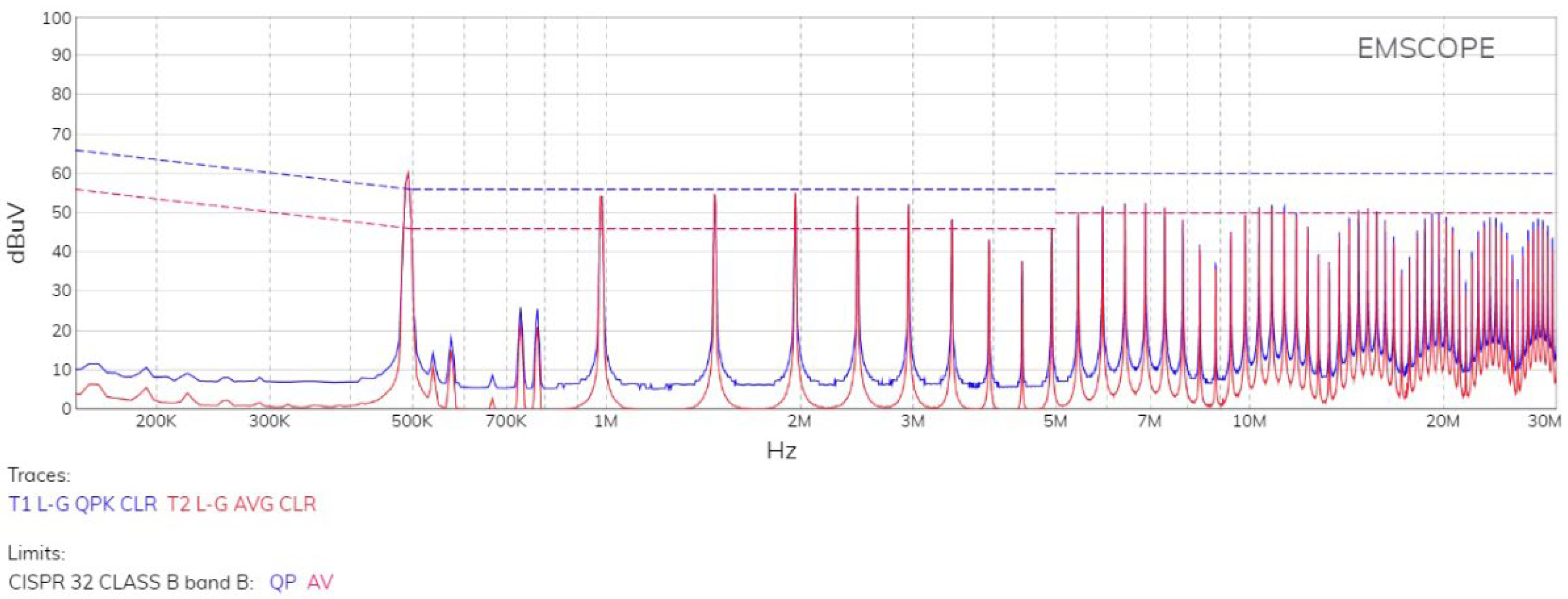
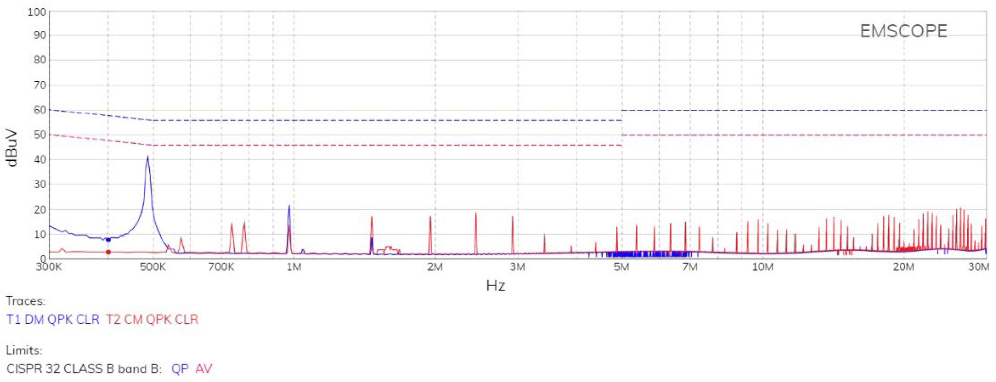
5.2. Conducted Emissions Measurements

In this subsection, the CE of the Boost converter Model MCP1640EV-SBC has been measured. The setup for the conducted emissions measurements described in Section 3 (Figure 4b) is seen in Figure 13.
Figure 14 shows the CE measurement at the positive terminal (+) of the Boost converter using the quasi-peak (QPK) and average (AVG) detectors (similar results are obtained in the negative terminal (−)). It can be seen that at 500 kHz, the registered measurement is above the CISPR 32 class B limit [2] for both detectors. A minimum mitigation of 20 dB for the AVG detector is needed to meet this standard (a constant that will be later used to design its PLF).
Figure 15 shows the modal decomposition of the CE noise generated by the EUT, i.e., the CM and DM CE measured using the QPK detector. As it can be seen, the DM is the dominant mode, and this is, along with the input impedance (or S-parameters), essential information to design a suitable PLF. The CM emissions are far below the limit and, therefore, do not need further mitigation.

5.3. PLF Design for the Boost Converter

Looking at the emissions of Figure 15, it seems obvious that this EUT does not need a CM choke because CM and CE are far below the limit. Therefore, the specific PLF for this EUT needs to be implemented using those components that mainly affect the DM, i.e., the X-type capacitors.
Considering that a minimum reduction of 20 dB is needed for the DM CE (so that the AVG detection falls below the limit), the question now is which capacitor value could be used to obtain such mitigation at 500 kHz. In order to avoid tedious trial-and-error practices, the methodology described in Section 4 has been applied. The PLF simulated consists of only an X-type capacitor, as shown in Figure 16.
The procedure described in Section 4.2 (step 6) is repeated, giving different values to the capacitor until an IL of 20 dB is achieved, obtaining a value of 2.6 μF (Figure 16, PLF1). For an X-type capacitor, this is a very high value (since typical commercial values go up to 0.47 μF). Therefore, a good alternative is to add an additional component to the circuit, i.e., to increment the order of the PLF, which allows the relaxation of the capacitor value while keeping the same attenuation at 500 kHz.
Figure 17 and Figure 18 show two possibilities for a second-order filter (PLF2 and PLF3), both composed of a capacitor and a normal inductor in each line. Due to the use of different configurations of PLFs, the resulting input impedances of the DC-DC converter will also be different. Therefore, both circuits will present different mitigation at the LISN ports. The circuit models of Section 2 show that the input impedance of the converter is capacitive (due to CIN), which means that the best option should be PLF2 since it is the one that maximizes the mismatch between its input impedance and the input impedance of the DC-DC converter.
The procedure described in Section 4.2 is repeated again for these two filters. The inductance values for PLF2 can be easily found by fixing the value of the capacitor to 0.47 μF (which is a standard value) and giving values to both inductors until an IL of 20 dB is achieved. In this particular example, an inductance of 1 μH was obtained.
Figure 19 shows the simulated DM IL achieved using PLF1 (composed of a single X-type capacitor of 2.6 μF), PLF2 (composed of two inductors of 1 μH at the load side and an X-type capacitor of 0.47 μF at the line side), and PLF3 using the same values as in PLF2 (that is, an X-type capacitor of 0.47 μF at the load side and two inductors of 1 μH at the line side). The IL for the three cases has been obtained by applying the procedure of Section 4.2 and, in particular, using (6). As expected, PLF3 has a negligible effect on the CE, while PLF2, which has the same components but in the correct configuration/order, obtains the desired IL. PLF3 can achieve the 20 dB of IL using inductors much larger (149 μH in this case), but this is not an optimal implementation, and therefore, it is discarded as a solution.
Although isolated inductors are not typical components in PLFs, they can also be used. An alternative, but more bulky option, is to use, as a DM inductance, the leakage inductance of a CM choke, which can achieve values between 1–3% of the total inductance of the choke (with the benefit of additional mitigation on the CM, which may be needed in other applications).
The PLF obtained has been implemented and tested. Figure 20 shows the CM and DM CE measured with the QPK detector. As expected, an attenuation of 20 dB is obtained.
This result shows that the optimal structure for a PLF to be connected to a DC-DC converter, as the ones shown in this paper, is composed of an inductance at the load side of the PLF (that can also be implemented using a CM choke), and an X-type capacitor at the line side of the PLF, which differ from the typical structures provided by commercial PLFs (as seen in Figure 13). Fixing the value of the X-type capacitor, any EMC engineer can easily find the value of the inductors (or the CM choke) and implement the optimal PLF quickly and accurately to mitigate the CE under the threshold level, even without obtaining the proper characterization of the EUT. This result also shows that even in those cases where the dominant mode is the DM, increasing the value of the X-type capacitor may not be enough to obtain the desired mitigation. Moreover, this problem worsens if the switching frequency decreases since a smaller cutoff frequency could be needed.
Another consideration is that different SMPS, which can be contained in different types of enclosures made of different types of materials, may produce different CE (where the CM may become predominant). In that case, and following the methodology described in this paper, the CM choke value and the Y-type capacitor values, along with their optimal position inside the PLF, can easily be found. Therefore, this paper provides a good basis for establishing a reliable standard method to design optimal PLFs for any electric and electronic product.

6. Conclusions

Commercial PLFs provide standard structures that may not be optimal for specific EUTs. In this paper, the input impedances of three different DC-DC converters, a Buck converter, a Boost converter, and a SEPIC converter, have been measured and modeled using circuit models to analyze their differences and determine the optimal PLF topology for each case. However, due to a common input capacitor in all circuits, typically used to stabilize the input DC voltage of the converter and mitigate the CE, all three converters present a similar input impedance. Therefore, the same PLF structure can be used for all of them.
Analyzing the CE of the Boost converter and using a circuit simulator that contains its S-parameter characterization, the optimal PLF topology was found. Its internal structure contains an inductance on both lines at the load side of the PLF to mitigate the DM noise (that can also be implemented using a CM choke) and an X-type capacitor between lines at the line side of the PLF. This structure differs from typical structures used in commercial PLFs and obtains optimal IL results with fewer and smaller components. From now, EMC engineers with the necessity to design the PLF for similar DC-DC converters will be able to depart from the PLF structure presented in this paper, reducing the time and cost devoted to EMC and accelerating the time-to-market.

Author Contributions

Conceptualization, M.B., A.-M.S. and F.J.P.; supervision, A.-M.S., F.J.P. and L.P.; writing—review and editing, M.B., A.-M.S. and F.J.P.; final revision, L.P. and A.C. All authors have read and agreed to the published version of the manuscript.

Funding

This research received no external funding.

Data Availability Statement

The data presented in the study are available in the article.

Conflicts of Interest

The authors declare no conflict of interest.

References

  1. CISPR 16-1-1; Specification for Radio Disturbance and Immunity Measuring Apparatus and Methods—Part 1-1: Radio Disturbance and Immunity Measuring Apparatus—Measuring apparatus. International Electrotechnical Commission: Geneva, Switzerland, 2019.
  2. CISPR 32:2015+AMD1:2019 CSV; Electromagnetic Compatibility of Multimedia Equipment—Emission Requirements. International Electrotechnical Commission: Geneva, Switzerland, 2015.
  3. Jayasree, P.; Priya, J.; Poojita, G.; Kameshwari, G. EMI Filter Design for Reducing Common-Mode and Differential-Mode Noise in Conducted Interference. Int. J. Electron. Commun. Eng. 2012, 5, 319–329. [Google Scholar]
  4. Tarateeraseth, V.; See, K.Y.; Wang, L.B.; Canavero, F.G. Systematic power line EMI filter design for SMPS. In Proceedings of the 10th International Symposium on Electromagnetic Compatibility, York, UK, 26–30 September 2011. [Google Scholar]
  5. Biela, J.; Wirthmueller, A.; Waespe, R.; Heldwein, M.L.; Raggl, K.; Kolar, J.W. Passive and Active Hybrid Integrated EMI Filters. IEEE Trans. Power Electron. 2009, 24, 1340–1349. [Google Scholar] [CrossRef]
  6. Zamazal, M.; Urbanec, T. Variable impedance in measuring EMI filter’s insertion loss. In Proceedings of the 2005 Asia-Pacific Conference on Communications, Perth, WA, Australia, 3–5 October 2005; pp. 24–27. [Google Scholar]
  7. Pérez, A.; Sánchez, A.-M.; Regué, J.; Ribó, M.; Rodríguez-Cepeda, P.; Pajares, F. Characterization of Power-Line Filters and Electronic Equipment for Prediction of Conducted Emissions. IEEE Trans. Electromagn. Compat. 2008, 50, 577–585. [Google Scholar] [CrossRef]
  8. Pérez, A.; Sanchez, A.M.; Regue, J.R.; Ribó, M.; Aquilué, R.; Rodriguez-Cepeda, P.; Pajares, F.J. Circuital and Modal Characterization of the Power-Line Network in the PLC Band. IEEE Trans. Power Deliv. 2009, 24, 1182–1189. [Google Scholar] [CrossRef]
  9. Sánchez, A.-M.; Pignari, S.A.; Regué, J.-R.; Ribó, M. Device Modeling for Nonstationary Conducted Emissions Based on Frequency- and Time-Domain Measurements. IEEE Trans. Electromagn. Compat. 2012, 54, 738–746. [Google Scholar] [CrossRef]
  10. Sánchez, A.; Regué, J.; Ribó, M.; Pérez, A.; Rodríguez-Cepeda, P.; Pajares, F. Automated Power-Line Filter Design under High 50-Hz Current Load Conditions. IEEE Trans. Electromagn. Compat. 2013, 55, 717–724. [Google Scholar] [CrossRef]
  11. Negri, S.; Spadacini, G.; Grassi, F.; Pignari, S.A. Prediction of EMI Filter Attenuation in Power-Electronic Converters via Circuit Simulation. IEEE Trans. Electromagn. Compat. 2022, 64, 1086–1096. [Google Scholar] [CrossRef]
  12. CISPR 17:2011; Methods of Measurement of the Suppression Characteristics of Passive EMC Filtering Devices. International Electrotechnical Commission: Geneva, Switzerland, 2011.
  13. Munir, H.A.; Jenu, M.Z.M.; Abdullah, M.F.L. Analysis and design of EMI filters to mitigate conducted emissions. In Proceedings of the Student Conference on Research and Development, Shah Alam, Malaysia, 17 July 2002; pp. 204–207. [Google Scholar] [CrossRef]
  14. Nussbaumer, T.; Heldwein, M.L.; Kolar, J.W. Common mode EMC input filter design for a three-phase buck-type PWM rectifier system. In Proceedings of the Twenty-First Annual IEEE Applied Power Electronics Conference and Exposition, Dallas, TX, USA, 19–23 March 2006; p. 7. [Google Scholar] [CrossRef]
  15. Luo, F.; Dong, D.; Boroyevich, D.; Mattavelli, P.; Wang, S. Improving high-frequency performance of an input common mode EMI filter using an impedance-mismatching filter. IEEE Trans. Power Electron. 2014, 29, 5111–5115. [Google Scholar] [CrossRef]
  16. Kotny, J.L.; Duquesne, T.; Idir, N. EMI Filter design using high frequency models of the passive components. In Proceedings of the IEEE Workshop on Signal Propagation on Interconnects (SPI 2011), Naples, Italy, 8–11 May 2011. [Google Scholar]
  17. Narayanasamy, B.; Jalanbo, H.; Luo, F. Development of Software to Design Passive Filters for EMI Suppression in SiC DC Fed Motor Drives. In Proceedings of the IEEE 3rd Workshop on Wide Bandgap Power Devices and Applications (WiPDA 2015), Blacksburg, VA, USA, 2–4 November 2015; pp. 230–235. [Google Scholar]
  18. Zhang, D.; Fan, T.; Ning, P.; Wen, X. An automatic EMI filter design methodology for electric vehicle application. In Proceedings of the 2017 IEEE Energy Conversion Congress and Exposition (ECCE), Cincinnati, OH, USA, 1–5 October 2017; pp. 4497–4503. [Google Scholar] [CrossRef]
  19. Wang, F.; Shen, W.; Boroyevich, D.; Ragon, S.; Stefanovic, V.; Arpilliere, M. Design Optimization of Industrial Motor Drive Power Stage Using Genetic Algorithms. In Proceedings of the IEEE Industry Applications Conference, Tampa, FL, USA, 8–12 October 2006; pp. 2581–2586. [Google Scholar]
  20. Giglia, G.; Ala, G.; Di Piazza, M.C.; Giaconia, G.C.; Luna, M.; Vitale, G.; Zanchetta, P. Automatic EMI Filter Design for Power Electronic Converters Oriented to High Power Density. Electronics 2018, 7, 9. [Google Scholar] [CrossRef] [Green Version]
  21. Danilovic, M.; Luo, F.; Xue, L.; Wang, R.; Mattavelli, P.; Boroyevich, D. Size and weight dependence of the single stage input EMI filter on switching frequency for low voltage bus aircraft applications. In Proceedings of the 15th International Power Electronics and Motion Control Conference (PEMC 2012), Novi Sad, Serbia, 4–6 September 2012; pp. LS4a.41–LS4a.47. [Google Scholar]
  22. Raggl, K.; Nussbaumer, T.; Kolar, J.W. Guideline for a Simplified Differential-Mode EMI Filter Design. IEEE Trans. Ind. Electron. 2010, 57, 1031–1040. [Google Scholar] [CrossRef]
  23. Ala, G.; Di Piazza, M.C.; Giaconia, G.C.; Giglia, G.; Luna, M.; Vitale, G.; Zanchetta, P. Computer Aided Optimal Design of High Power Density EMI Filters. In Proceedings of the IEEE 16th International Conference on Environment and Electrical Engineering (EEEIC 2016), Florence, Italy, 7–10 June 2016; pp. 1–6. [Google Scholar]
  24. Wang, S.; Lee, F.C.; Odendaal, W.G. Characterization and parasitic extraction of EMI filters using scattering parameters. IEEE Trans. Power Electron. 2005, 20, 502–510. [Google Scholar] [CrossRef]
  25. Wang, S.; Lee, F.C.; Chen, D.Y.; Odendaal, W.G. Effects of parasitic parameters on the performance of EMI filters. IEEE Trans. Power Electron. 2004, 19, 869–877. [Google Scholar] [CrossRef]
  26. Luo, F.; Boroyevich, D.; Mattavelli, P. Improving EMI filter design within circuit impedance mismatching. In Proceedings of the 2012 Twenty-Seventh Annual IEEE Applied Power Electronics Conference and Exposition (APEC), Orlando, FL, USA, 5–9 February 2012; pp. 1652–1658. [Google Scholar] [CrossRef]
  27. Kovacic, M.; Hanic, Z.; Stipetic, S.; Krishnamurthy, S.; Zarko, D. Analytical Wideband Model of a Common-Mode Choke. IEEE Trans. Power Electron. 2012, 27, 3173–3185. [Google Scholar] [CrossRef]
  28. Nave, M.J. On Modeling the Common Mode Inductor. In Proceedings of the IEEE 1991 International Symposium on Electromagnetic Compatibility, Cherry Hill, NJ, USA, 12 July–16 August 1991. [Google Scholar]
  29. IHernandez, I.; de Leon, F.; Gomez, P. Design Formulas for the Leakage Inductance of Toroidal Distribution Transformers. IEEE Trans. Power Deliv. 2011, 26, 2197–2204. [Google Scholar] [CrossRef]
  30. Ren, R.; Dong, Z.; Liu, B.; Wang, F. Leakage Inductance Estimation of Toroidal Common-mode Choke from Perspective of Analogy between Reluctances and Capacitances. In Proceedings of the 2020 IEEE Applied Power Electronics Conference and Exposition, New Orleans, LA, USA, 15–19 March 2020; pp. 2822–2828. [Google Scholar] [CrossRef]
  31. Shih, F.-Y.; Chen, D.; Wu, Y.-P.; Chen, Y.-T. A procedure for designing EMI filters for AC line applications. IEEE Trans. Power Electron. 1996, 11, 170–181. [Google Scholar] [CrossRef]
  32. Lai, Y.-S.; Chen, P.-S. New EMI Filter Design Method for Single Phase Power Converter Using Software-Based Noise Separation Method. In Proceedings of the 2007 IEEE Industry Applications Annual Meeting, New Orleans, LA, USA, 23–27 September 2007; pp. 2282–2288. [Google Scholar] [CrossRef]
  33. Xu, D.; Gao, Q.; Wang, W. Design of a Passive Filter to Reduce Common-Mode and Differential-Mode Voltage Generated by Voltage-Source PWM Inverter. In Proceedings of the IECON 2006—32nd Annual Conference on IEEE Industrial Electronics, Paris, France, 6–10 November 2006; pp. 2483–2487. [Google Scholar] [CrossRef]
  34. Caponet, M.C.; Profumo, F.; Tenconi, A. EMI filters design for power electronics. In Proceedings of the 2002 IEEE 33rd Annual IEEE Power Electronics Specialists Conference. Proceedings (Cat. No.02CH37289), Cairns, QLD, Australia, 23–27 June 2002; Volume 4, pp. 2027–2032. [Google Scholar] [CrossRef]
  35. Bertoldi, B.; Junior, M.M.B.; Dall’Asta, M.S.; Greidanus, M.D.R. Modeling of SEPIC Converter with Non-Ideal Components in Continuous and Discontinuous Conduction Mode. In 2018 4th IEEE Southern Power Electronics Conference; IEEE: Piscataway, NJ, USA, 2018. [Google Scholar]
  36. Faifer, M.; Piegari, L.; Rossi, M.; Toscani, S. An Average Model of DC–DC Step-Up Converter Considering Switching Losses and Parasitic Elements. Energies 2021, 14, 7780. [Google Scholar] [CrossRef]
  37. Abid, R.; Masmoudi, F.; Ben Salem, F.; Derbel, N. Modeling and simulation of conventional DC-DC converters deticated to photovoltaic applications. In Proceedings of the 2016 7th International Renewable Energy Congress (IREC), Hammamet, Tunisia, 22–24 March 2016; pp. 1–6. [Google Scholar]
  38. Chander, S.; Agarwal, P.; Gupta, I. Design, modeling and simulation of DC-DC converter. In Proceedings of the 2010 Conference Proceedings IPEC, Singapore, 27–29 October 2010; pp. 456–461. [Google Scholar]
  39. CISPR 16-2-1:2014+AMD1:2017; Specification for Radio Disturbance and Immunity Measuring Apparatus and Methods—Part 2-1: Methods of Measurement of Disturbances and Immunity—Conducted Disturbance Measurements. International Electrotechnical Commission: Geneva, Switzerland, 2017.
  40. Bosi, M.; Sanchez, A.-M.; Pajares, F.; Garcia, I.; Accensi, J.; Regue, J. Common- and Differential-Mode Conducted Emissions Measurements using Conventional Receivers versus FFT-Based Receivers. IEEE Electromagn. Compat. Mag. 2022, 11, 55–63. [Google Scholar] [CrossRef]
Figure 1. Model of Buck converter including parasitic components.
Energies 16 02085 g001
Figure 2. Model of the Boost converter, including non-ideal components.
Energies 16 02085 g002
Figure 3. Model of SEPIC converter including non-ideal components.
Energies 16 02085 g003
Figure 4. (a) S-parameter measurement setup; (b) CE measurement setup.
Energies 16 02085 g004
Figure 5. Equivalent circuit of the EUT connected to the equivalent circuit of a LISN according to CISPR 16.
Energies 16 02085 g005
Figure 6. PLF connected between the equivalent circuit of a EUT and the equivalent circuit of a LISN according to CISPR 16.
Energies 16 02085 g006
Figure 7. Typical structure of a PLF.
Energies 16 02085 g007
Figure 8. S-parameters measurement setup, which contains a EUT (front row, left side, placed above the foam), a VNA (right side) connected to two transient limiters, a two-port LISN (background, middle) and a programmable DC power supply (background, left side).
Energies 16 02085 g008
Figure 9. Comparison of the S-parameters obtained by simulations (red), EUT powered (blue), and EUT not powered (pink) for the Buck Converter Model LM2596.
Energies 16 02085 g009
Figure 10. Comparison of the S-parameters obtained by simulations (red), EUT not powered (pink), and EUT powered (blue) for the Boost Converter Model MCP1640EV-SBC.
Energies 16 02085 g010aEnergies 16 02085 g010b
Figure 11. Comparison of the S-parameters obtained by simulations (red), EUT not powered (pink), and EUT powered (blue) for the SEPIC Converter Model MCP1663.
Energies 16 02085 g011
Figure 12. Comparison of the S-parameters obtained by simulations (red), EUT not powered (pink), and EUT powered (blue) for the SEPIC Converter Model MCP1663 after removing CIN.
Energies 16 02085 g012
Figure 13. CE measurement setup, which contains a EUT (front row), an EMSCOPE (a two-port EMI receiver, background, left side), and a two-port LISN (background, right side).
Energies 16 02085 g013
Figure 14. CE measurement at the positive terminal (‘+’) of the Boost converter using the quasi-peak (QPK, blue) and average (AVG, red) detectors. Amplitude units are in dBμV, and Frequency units are in Hz.
Energies 16 02085 g014
Figure 15. CM (red) and DM (blue) decomposition of the CE measurement of the Boost converter using the QPK detector. Amplitude units are in dBμV, and Frequency units are in Hz.
Energies 16 02085 g015
Figure 16. PLF connected between the EUT and the LISN consisting of only an X-type capacitor.
Energies 16 02085 g016
Figure 17. PLF connected between the EUT and the LISN consisting of an X-type capacitor and a DM inductor.
Energies 16 02085 g017
Figure 18. PLF connected between the EUT and the LISN consisting of a DM inductor and an X-type capacitor.
Energies 16 02085 g018
Figure 19. DM IL of PLF1 (solid red line), PLF2 (dotted blue line), and PLF3 (dashed pink line).
Energies 16 02085 g019
Figure 20. CM (red) and DM (blue) were obtained with a filter composed of a Cx = 0.47 uF and an L = 0.99 uH. Amplitude units are in dBμV, and Frequency units are in Hz.
Energies 16 02085 g020
Table 1. Values of the parasitic components of the Buck Converter model LM2596.
SymbolDescriptionValue
CPARParasitic capacitance14 pF
Lpar1Parasitic inductance56 nH
Lpar2Parasitic inductance1 nH
rS, rD, rC, rLParasitic resistances200 mΩ
Table 2. Values of the parasitic components of the Boost converter Model MCP1640EV-SBC.
SymbolDescriptionValue
CPARParasitic capacitance10 pF
Lpar1Parasitic inductance199 nH
Lpar2Parasitic inductance199 nH
rS, rD, rC, rLParasitic resistances200 mΩ
Table 3. Values of the parasitic components of the SEPIC converter model MCP1663.
SymbolDescriptionValue
CPARParasitic capacitance21 pF
Lpar1Parasitic inductance33 nH
Lpar2Parasitic inductance9 nH
rS, rD, rC1, rL1, rC2, rL2Parasitic resistances200 mΩ
Disclaimer/Publisher’s Note: The statements, opinions and data contained in all publications are solely those of the individual author(s) and contributor(s) and not of MDPI and/or the editor(s). MDPI and/or the editor(s) disclaim responsibility for any injury to people or property resulting from any ideas, methods, instructions or products referred to in the content.

