
A High-Power Solar PV-fed TISO DC-DC Converter for Electric Vehicle Charging Applications

 , and
, and
Abstract
:1. Introduction
2. Related Works
- (i)
- Design of a 100 W TISO converter and implementation of a novel control strategy for MPPT tracking and voltage regulation simultaneously.
- (ii)
- Model development of designed system with proposed controller in MATLAB/Simulink.
- (iii)
- Analysis of output voltage stability in terms of output voltage ripple using P&O, multiple step size P&O, and proposed control approach.
- (iv)
- Simulation and analysis of the proposed approach under various conditions.
- (v)
- Performance analysis of a high-power converter with proposed control technique.
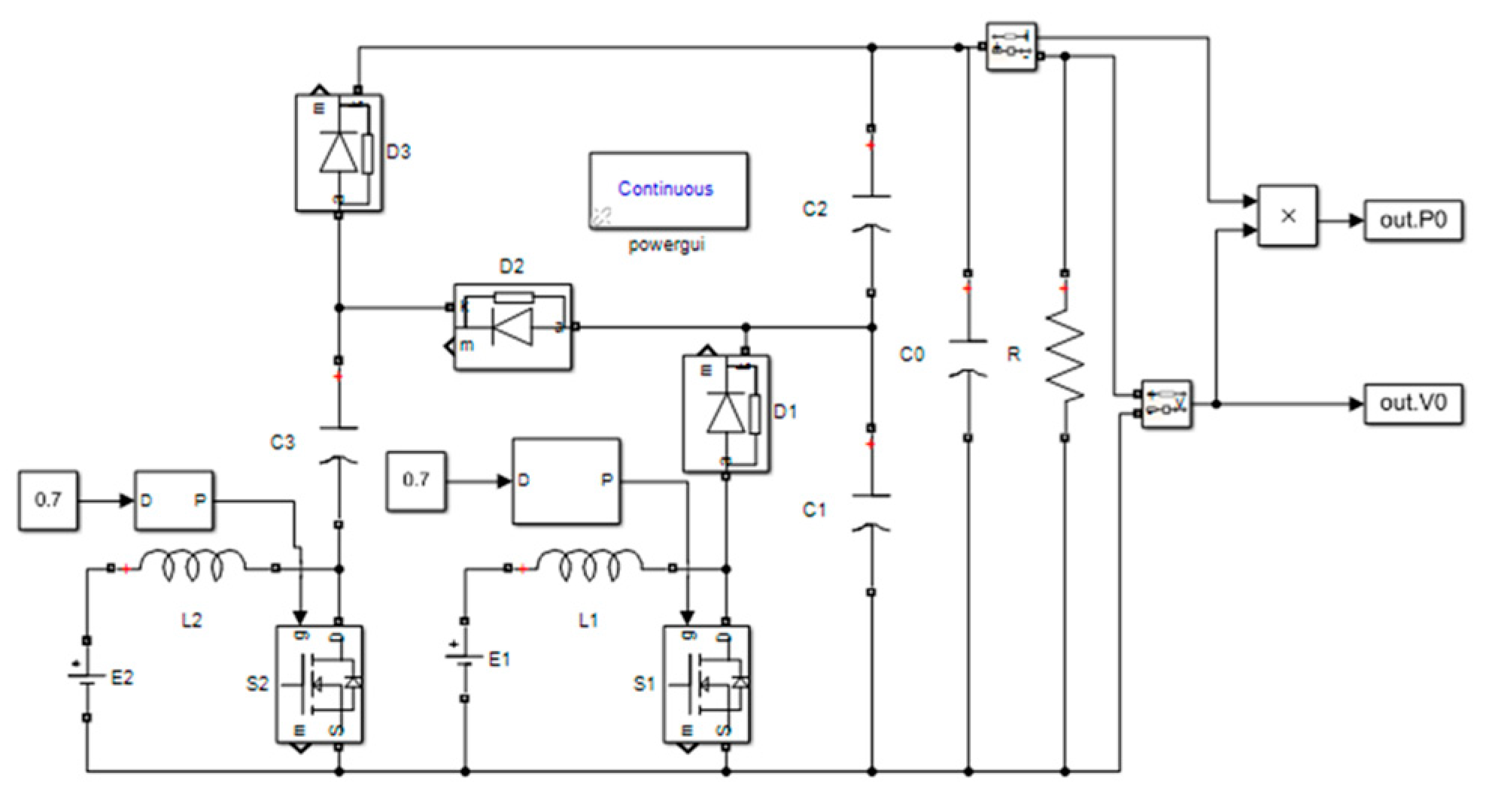
3. Two-Input Single-Output (TISO) DC-DC Converter
E2 − VC2 (1 − d2) = 0
3.1. Selection of Load Resistance
3.2. Selection of Inductor Values
3.3. Selection of Capacitor Values
4. Simulation Results and Discussion
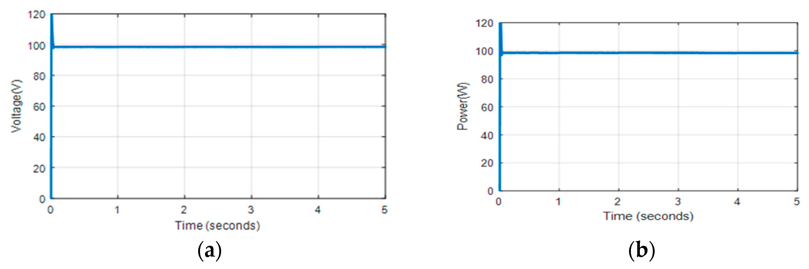
4.1. Conventional Circuit
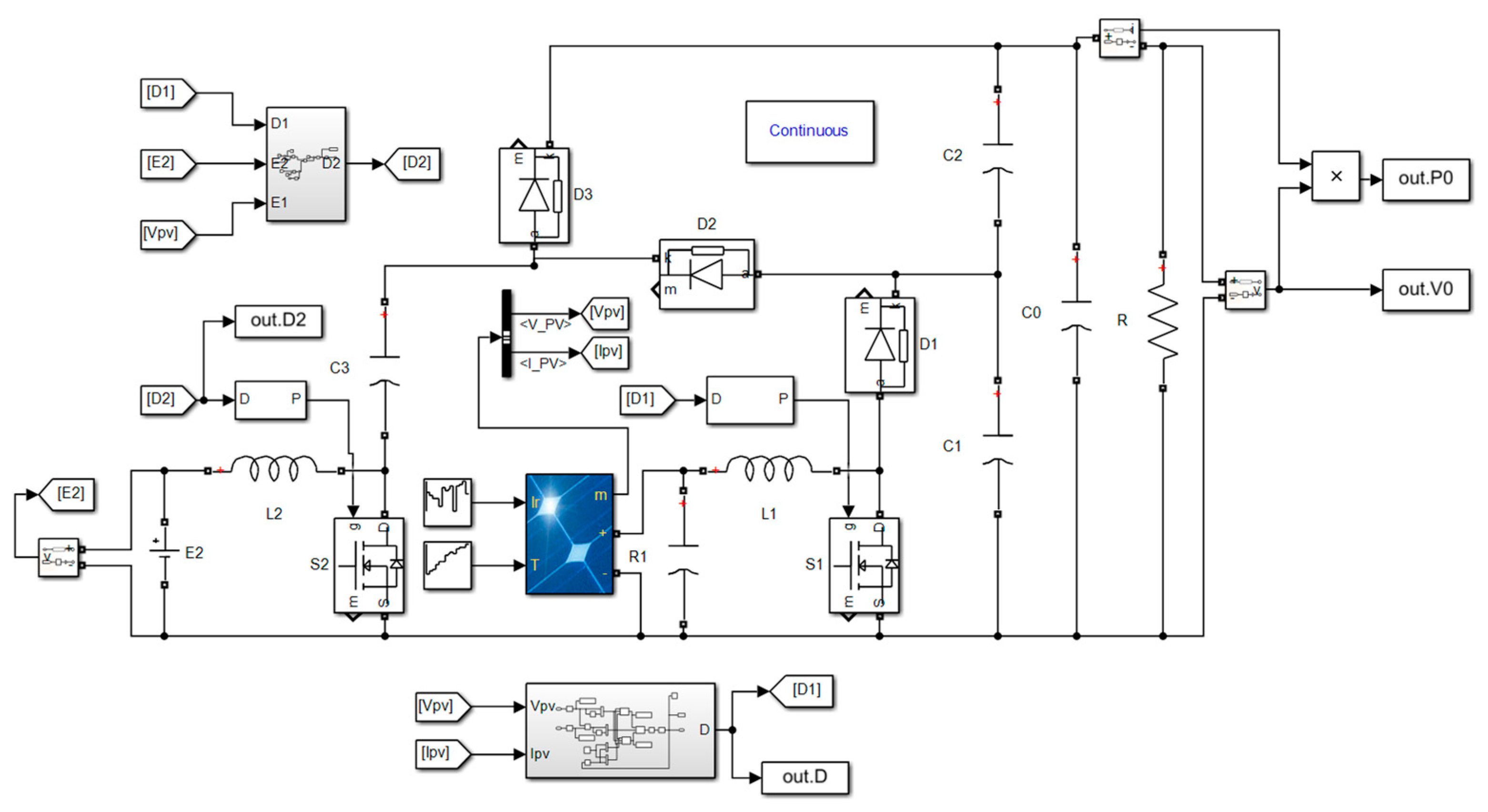
4.2. TISO DC−DC Converter with Solar PV Input
4.2.1. MPPT Tracking Algorithms
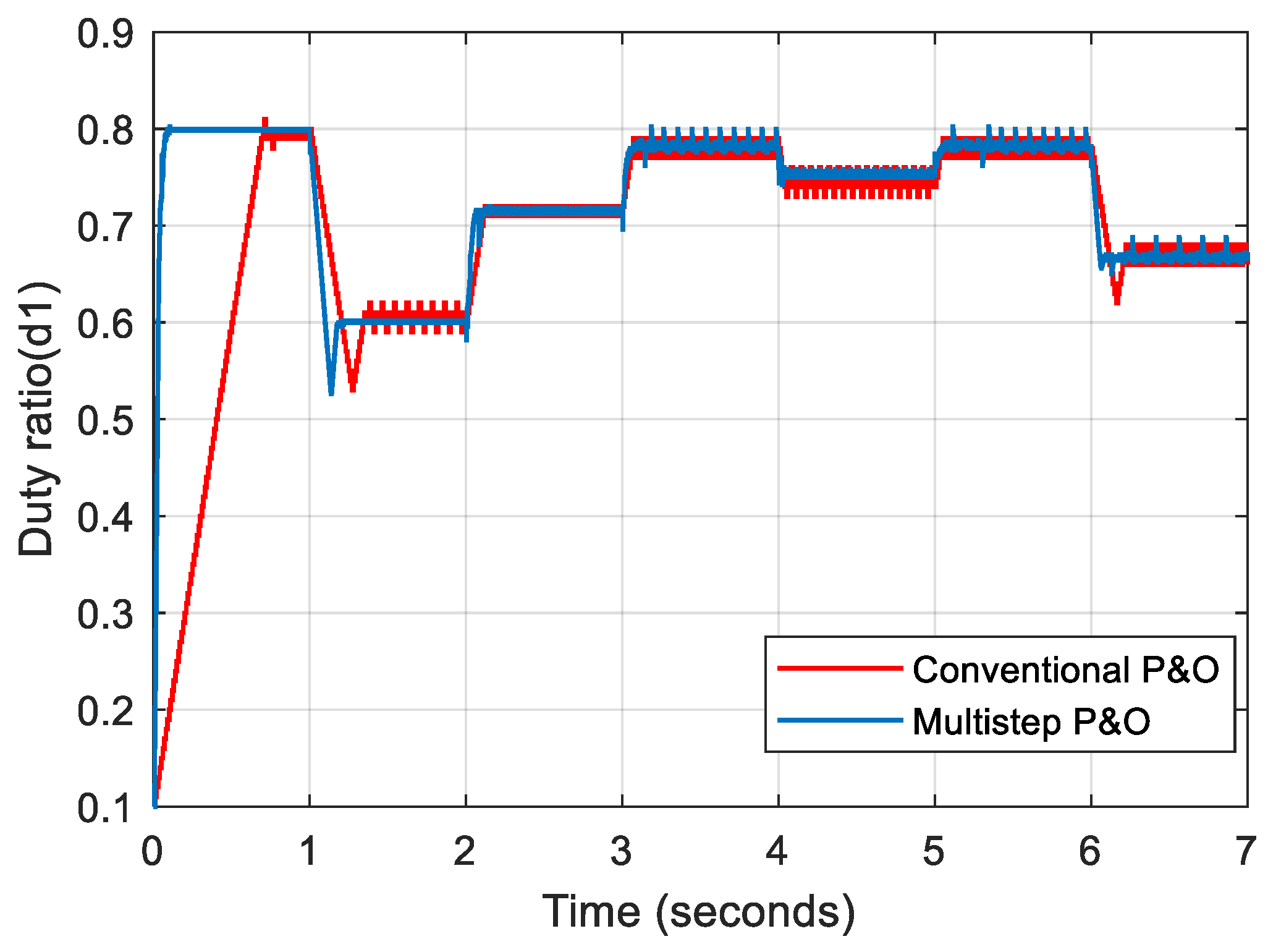
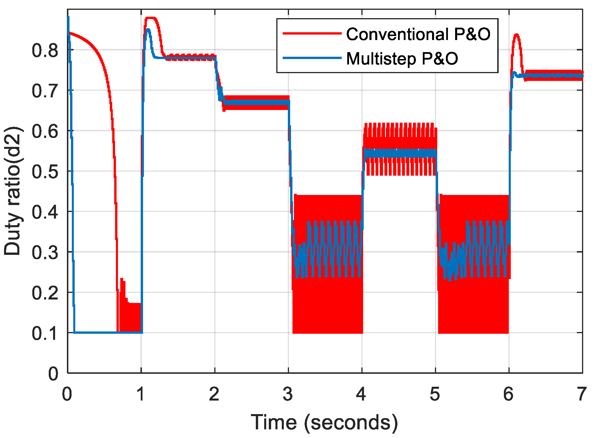
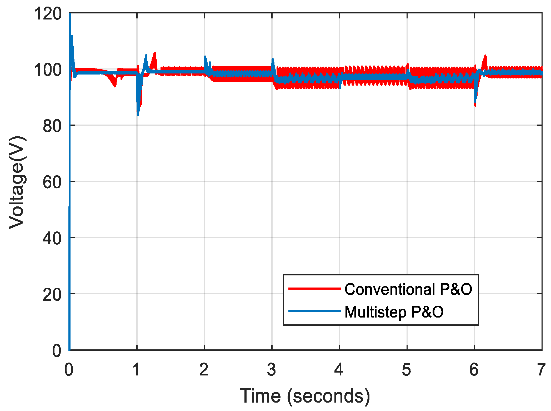
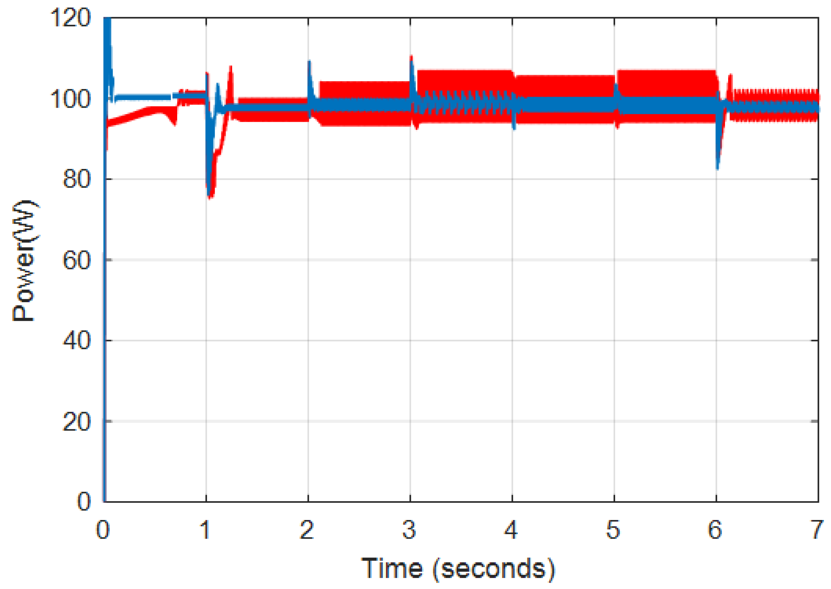
4.2.2. Analysis of TISO DC-DC Converter with Solar PV
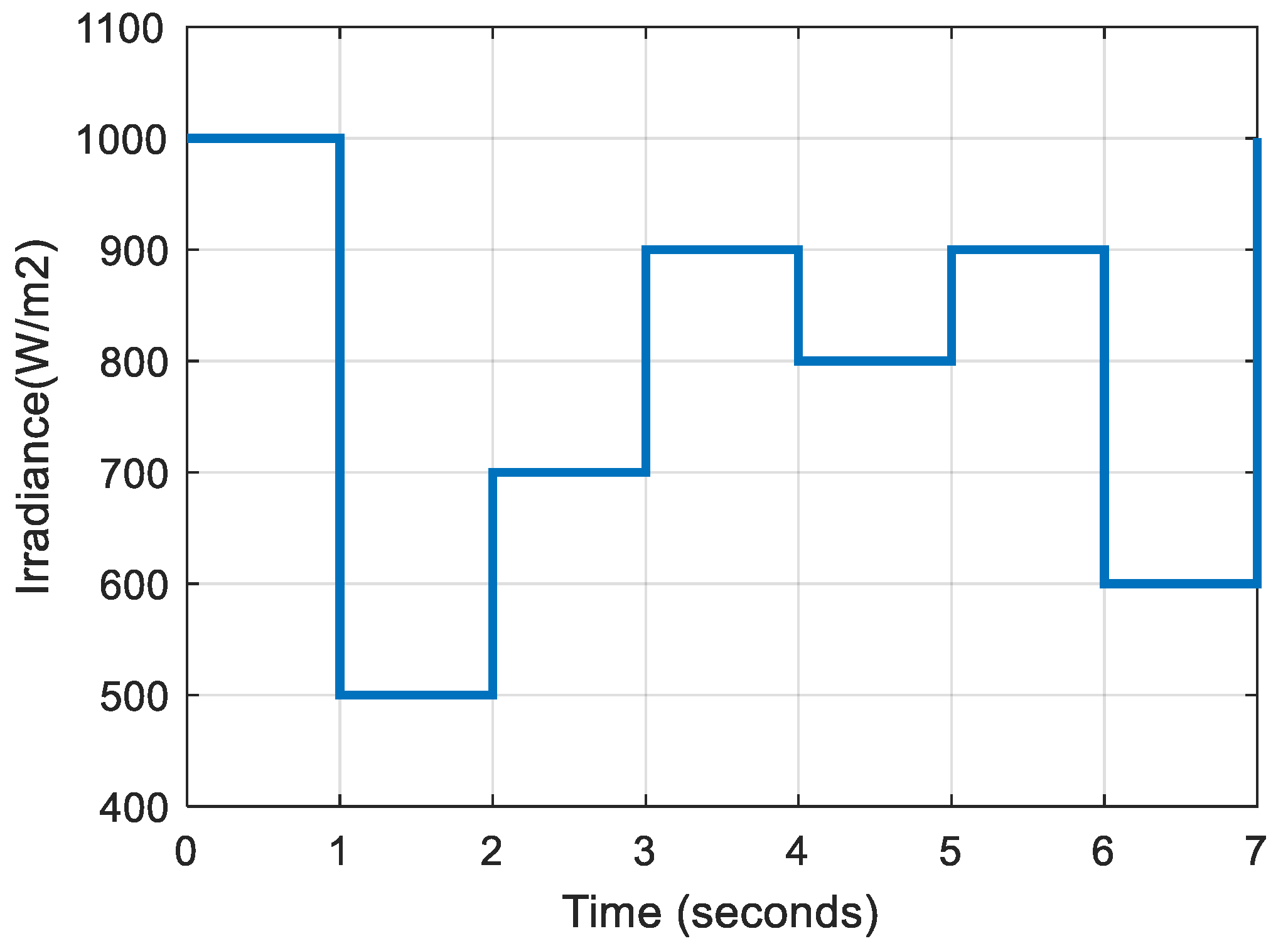
4.2.3. Analysis under Changing Irradiation at a Constant Temperature
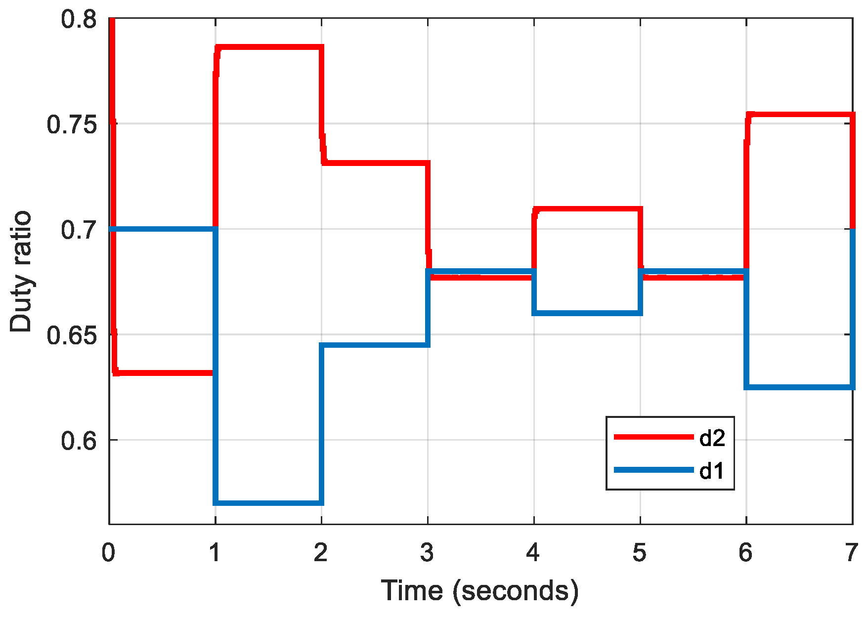
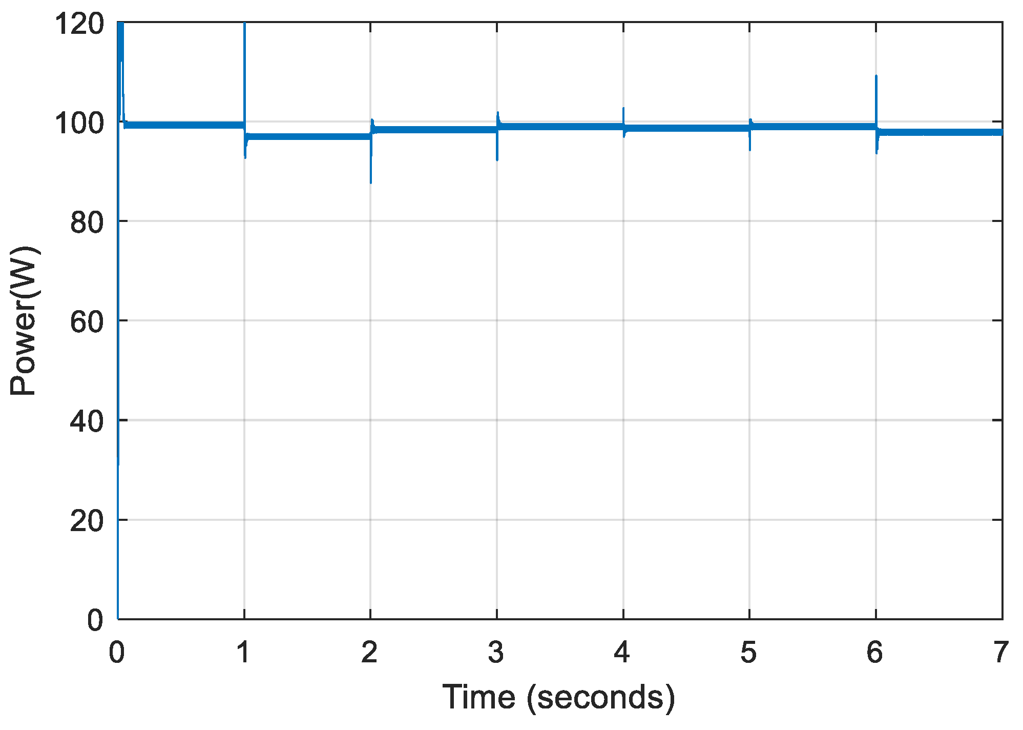
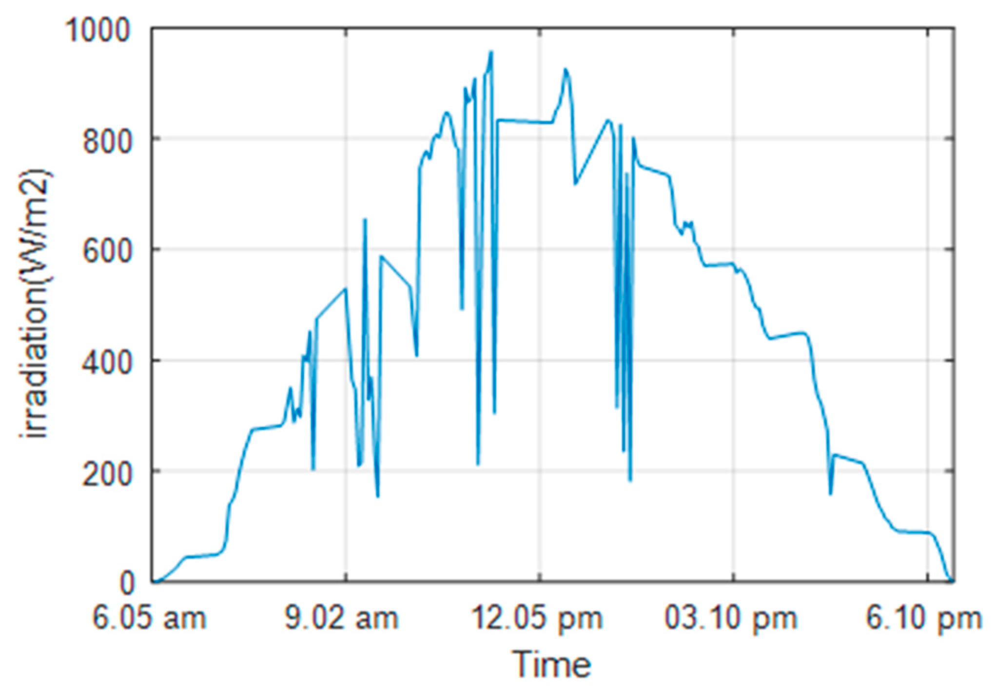
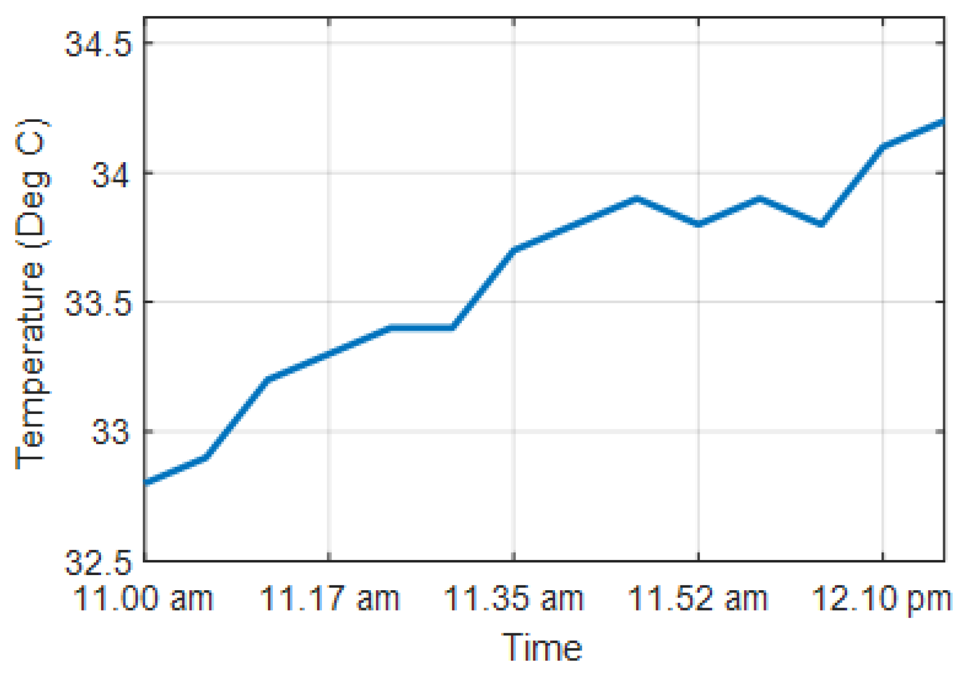
4.2.4. Analysis of Rapidly Changing Environmental Conditions with Real-Time Data
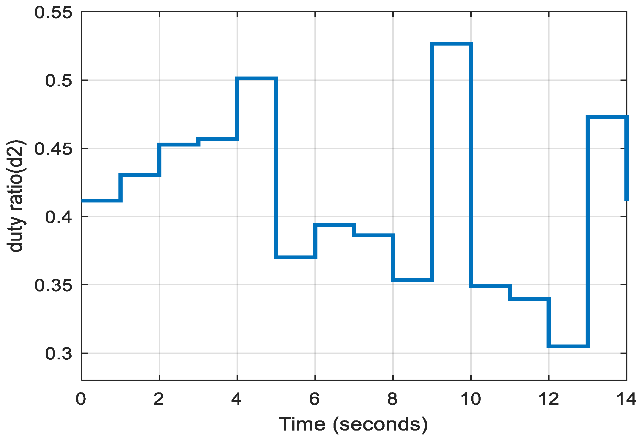
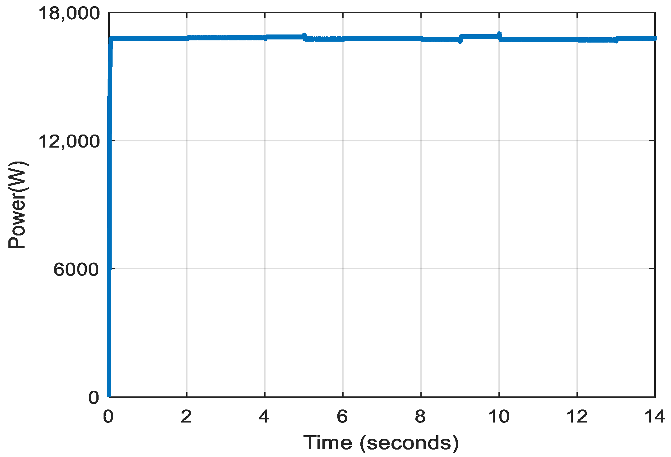
4.2.5. Analysis of High-Power Converter
5. Conclusions
Author Contributions
Funding
Conflicts of Interest
References
- Adib, A.; Shadmand, M.B.; Shamsi, P.; Afridi, K.K.; Amirabadi, M.; Fateh, F.; Ferdowsi, M.; Lehman, B.; Lewis, L.H.; Mirafzal, B.; et al. E-Mobility-Advancements and Challenges. IEEE Access 2019, 7, 165226–165240. [Google Scholar] [CrossRef]
- Mohammed, S.S.; Ahamed, T.I.; Aleem, S.H.A.; Omar, A.I. Interruptible Charge Scheduling for Plug-In Electric Vehicle to Minimize Charging Cost Using Heuristic Algorithm. Electr. Eng. 2021, 104, 1425–1440. [Google Scholar] [CrossRef]
- Titus, F.; Thanikanti, S.B.; Deb, S.; Kumar, N.M. Charge Scheduling Optimization of Plug-In Electric Vehicle in a PV Powered Grid-Connected Charging Station Based on Day-Ahead Solar Energy Forecasting in Australia. Sustainability 2022, 14, 3498. [Google Scholar] [CrossRef]
- Affam, A.; Buswig, Y.M.; Othman, A.-K.B.H.; Bin Julai, N.; Qays, O. A review of multiple input DC-DC converter topologies linked with hybrid electric vehicles and renewable energy systems. Renew. Sustain. Energy Rev. 2020, 135, 110186. [Google Scholar] [CrossRef]
- Reddy, K.J.; Natarajan, S. Energy sources and multi-input DC-DC converters used in hybrid electric vehicle applications–A review. Int. J. Hydrogen Energy 2018, 43, 17387–17408. [Google Scholar] [CrossRef]
- Dusmez, S.; Li, X.; Akin, B. A new multiinput three-level DC/DC converter. IEEE Trans. Power Electron. 2015, 31, 1230–1240. [Google Scholar] [CrossRef]
- Mangu, B.; Akshatha, S.; Suryanarayana, D.; Fernandes, B.G. Grid-Connected PV-Wind-Battery-Based Multi-Input Transformer-Coupled Bidirectional DC-DC Converter for Household Applications. IEEE J. Emerg. Sel. Top. Power Electron. 2016, 4, 1086–1095. [Google Scholar] [CrossRef]
- Ahrabi, R.R.; Ardi, H.; Elmi, M.; Ajami, A. A Novel Step-Up Multiinput DC-DC Converter for Hybrid Electric Vehicles Application. IEEE Trans. Power Electron. 2016, 32, 3549–3561. [Google Scholar] [CrossRef]
- KhademiAstaneh, P.; Javidan, J.; Valipour, K.; Akbarimajd, A. A bidirectional high step-up multi-input DC-DC converter with soft switching. Int. Trans. Electr. Energy Syst. 2018, 29, e2699. [Google Scholar] [CrossRef] [Green Version]
- Majeed, Y.E.; Ahmad, I.; Habibi, D. A Multiple-Input Cascaded DC-DC Converter for Very Small Wind Turbines. IEEE Trans. Ind. Electron. 2018, 66, 4414–4423. [Google Scholar] [CrossRef]
- Varesi, K.; Hosseini, S.H.; Sabahi, M.; Babaei, E. A high-voltage gain nonisolated noncoupled inductor based multi-input DC-DC topology with reduced number of components for renewable energy systems. Int. J. Circuit Theory Appl. 2017, 46, 505–518. [Google Scholar] [CrossRef]
- Kardan, F.; Alizadeh, R.; Banaei, M.R. A New Three Input DC/DC Converter for Hybrid PV/FC/Battery Applications. IEEE J. Emerg. Sel. Top. Power Electron. 2017, 5, 1771–1778. [Google Scholar] [CrossRef]
- Dhananjaya, M.; Pattnaik, S. Design and Implementation of a Multi-Input Single-Output DC-DC Converter. In Proceedings of the 1st IEEE International Conference on Sustainable Energy Technologies and Systems (ICSETS), Bhubaneswar, India, 26 February–1 March 2019; pp. 194–199. [Google Scholar] [CrossRef]
- Haghighian, S.K.; Tohidi, S.; Feyzi, M.R.; Sabahi, M. Design and analysis of a novel SEPIC-based multi-input DC/DC converter. IET Power Electron. 2017, 10, 1393–1402. [Google Scholar] [CrossRef]
- Varesi, K.; Hosseini, S.H.; Sabahi, M.; Babaei, E.; Vosoughi, N. Performance and design analysis of an improved non-isolated multiple input buck DC-DC converter. IET Power Electron. 2017, 10, 1034–1045. [Google Scholar] [CrossRef]
- Athikkal, S.; Sundaramoorthy, K.; Sankar, A. Design, fabrication and performance analysis of a two input-single output DC-DC converter. Energies 2017, 10, 1410. [Google Scholar] [CrossRef] [Green Version]
- Banaei, M.R.; Ardi, H.; Alizadeh, R.; Farakhor, A. Non-isolated multi-input-single-output DC/DC converter for photovoltaic power generation systems. IET Power Electron. 2014, 7, 2806–2816. [Google Scholar] [CrossRef]
- Erdal Irmak, N.G. Application of a boost based multi-input single-output DC/DC converter. In Proceedings of the 2017 IEEE 6th International Conference on Renewable Energy Research and Applications (ICRERA), San Diego, CA, USA, 5–8 November 2017; pp. 955–961. [Google Scholar]
- Mohammadi, S.; Dezhbord, M.; Babalou, M.; Azizkandi, M.E.; Hosseini, S.H. A New Non-Isolated Multi-Input DC-DC Converter with High Voltage gain and Low Average of Normalized Peak Inverse Voltage. In Proceedings of the 2019 10th International Power Electronics, Drive Systems and Technologies Conference (PEDSTC), Shiraz, Iran, 12–14 February 2019; pp. 515–520. [Google Scholar] [CrossRef]
- Deihimi, A.; Mahmoodieh, M.E.S.; Iravani, R. A new multi-input step-up DC–DC converter for hybrid energy systems. Electr. Power Syst. Res. 2017, 149, 111–124. [Google Scholar] [CrossRef]
- Liu, S.-L.; Liu, J.; Mao, H.; Zhang, Y.-Q. Analysis of operating modes and output voltage ripple of boost DC-DC converters and its design considerations. IEEE Trans. Power Electron. 2008, 23, 1813–1821. [Google Scholar] [CrossRef]
- Gorecki, P. Electrothermal Averaged Model of a Diode–IGBT Switch for a Fast Analysis of DC–DC Converters. IEEE Trans. Power Electron. 2022, 37, 13003–13013. [Google Scholar] [CrossRef]
- Górecki, K.; Detka, K. Influence of Power Losses in the Inductor Core on Characteristics of Selected DC–DC Converters. Energies 2019, 12, 1991. [Google Scholar] [CrossRef] [Green Version]
- Mohammed, S.S.; Devaraj, D.; Ahamed, T.I. Learning Automata and Soft Computing Techniques based Maximum Power Point Tracking for Solar PV Systems. In Intelligent Paradigms for Smart Grid and Renewable Energy Systems; Springer: Berlin/Heidelberg, Germany, 2020. [Google Scholar]
- Mohammed, S.S.; Devaraj, D.; Ahamed, T.I. A Novel Hybrid Maximum Power Point Tracking technique using Perturb & Observe Algorithm and Learning Automata for solar PV system. Energy 2016, 112, 1096–1106. [Google Scholar]
- John, R.; Mohammed, S.S.; Zachariah, R. Variable step size Perturb and observe MPPT algorithm for standalone solar photovoltaic system. In Proceedings of the 2017 IEEE International Conference on Intelligent Techniques in Control, Optimization and Signal Processing (INCOS), Srivilliputtur, India, 23–25 March 2017; pp. 1–6. [Google Scholar] [CrossRef]


| Description | Value |
|---|---|
| Input Voltage (E1) | 18 V |
| Input Voltage (E2) | 15 V |
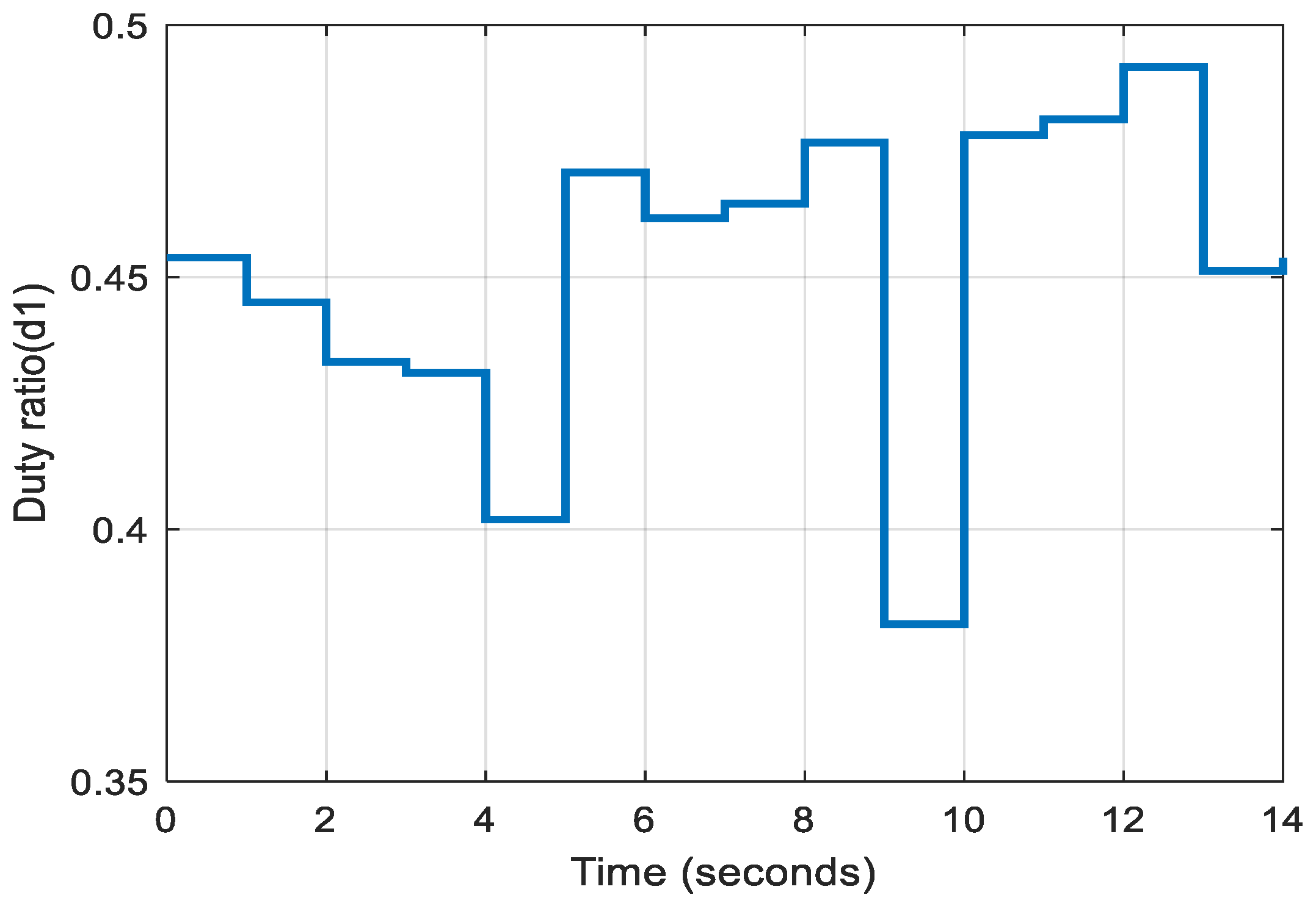
| Duty Ratio (d1 and d2) | 0.7 |
| Switching Frequency (f) | 15 kHz |
| Output Voltage (V0) | 100 V |
| Output Power (P0) | 100 W |
| Boost Inductance (L1 and L2) | 200 µH |
| Capacitance (C0, C1, C2, and C3) | 267 µF |
| Load Resistance (RL) | 100 Ω |
| Description | Value |
|---|---|
| Peak power (Pmax) | 100 W |
| Voltage at peak power (Vmax) | 18 V |
| Current at peak power (IMAX) | 5.56 A |
| Short-circuit current (Isc) | 6.06 A |
| Open-circuit voltage (Voc) | 22 V |
| Temperature coefficient of Isc | (0.06 ± 0.15)%/°C |
| Solar Irradiation (W/m2) | Time Delay in Seconds | Average Output Voltage (Vout) | Percentage of Ripple | Average Output Power (Pout) | Efficiency (η) | |||||
|---|---|---|---|---|---|---|---|---|---|---|
| Conv P&O | Multi P&O | Conv P&O | Multi P&O | Conv P&O | Multi P&O | Conv P&O | Multi P&O | Conv P&O | Multi P&O | |
| 1000 | 0.73 | 0.096 | 98.83 | 98.64 | 2.16% | 1.34% | 99.8 | 98.95 | 99.80% | 98.95% |
| 500 | 0.35 | 0.183 | 99.24 | 99.06 | 2.34% | 1.56% | 97.22 | 97.8 | 97.22% | 97.80% |
| 700 | 0.12 | 0.098 | 98.26 | 98.28 | 5.20% | 1.79% | 98.2 | 98.5 | 98.20% | 98.50% |
| 900 | 0.07 | 0.051 | 96.81 | 96.81 | 7.62% | 3.26% | 99.7 | 98.9 | 99.70% | 98.90% |
| 800 | 0.05 | 0.028 | 97.68 | 97.31 | 6.60% | 1.75% | 99.65 | 98.6 | 99.65% | 98.60% |
| 900 | 0.05 | 0.027 | 96.81 | 96.81 | 7.62% | 3.26% | 99.7 | 98.9 | 99.70% | 98.90% |
| 600 | 0.2 | 0.076 | 98.9 | 98.97 | 3.66% | 1.77% | 98.33 | 97.9 | 98.33% | 97.90% |
| Overall Average | 98.87 | 98.81 | 2.91% | 1.55% | 99.07 | 98.43 | 99.07% | 98.43% | ||
| Solar Irradiation (W/m2) | Average Output Voltage (Vout) | Percentage of Ripple | Average Output Power (Pout) | Efficiency (η) |
|---|---|---|---|---|
| 1000 | 99.03 V | 0.22% | 98.3 W | 98.30% |
| 500 | 98.93 V | 0.22% | 97.49 W | 97.49% |
| 700 | 98.92 V | 0.23% | 98.85 W | 98.85% |
| 900 | 98.62 V | 0.23% | 99.34 W | 99.34% |
| 800 | 99.09 V | 0.24% | 99.08 W | 99.08% |
| 900 | 98.62 V | 0.23% | 99.34 W | 99.34% |
| 600 | 98.92 V | 0.23% | 98.39 W | 98.39% |
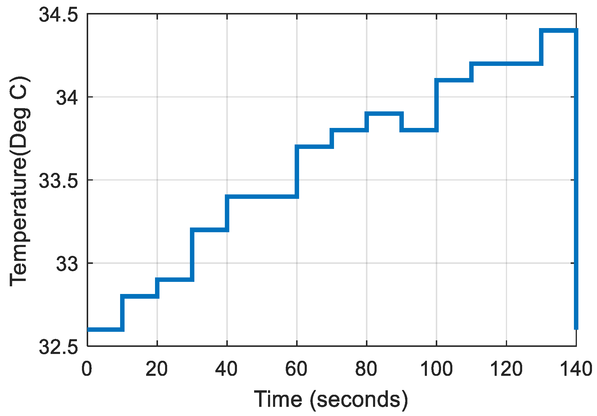
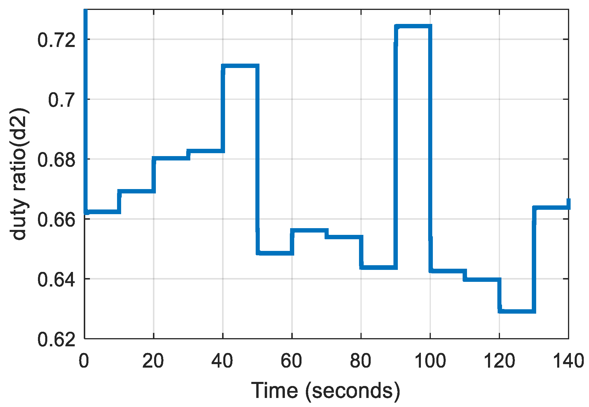
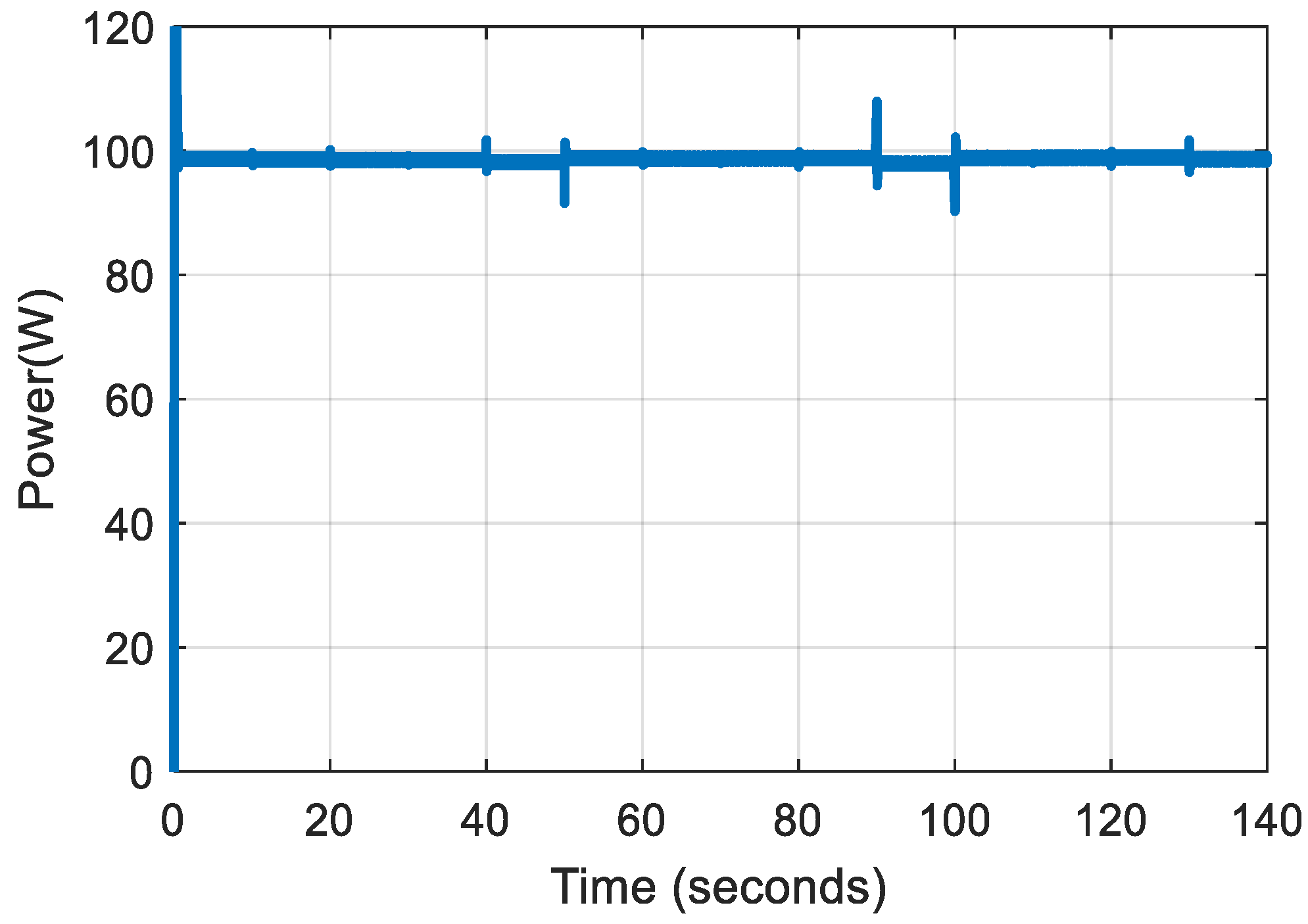
| Irradiation (W/m2) | Temperature (°C) | Average Output Voltage (Vout) | Percentage of Ripple | Average Output Power (Pout) | Efficiency (η) |
| 844.6 | 32.8 | 99.21 V | 0.22% | 98.73 W | 98.73% |
| 818.1 | 32.9 | 99.25 V | 0.23% | 98.65 W | 98.65% |
| 786.5 | 33.2 | 99.4 V | 0.22% | 98.65 W | 98.65% |
| 780.8 | 33.4 | 99.39 V | 0.23% | 98.51 W | 98.51% |
| 710.4 | 33.4 | 99.87 V | 0.22% | 98.18 W | 98.18% |
| 892.3 | 33.7 | 98.92 V | 0.22% | 98.83 W | 98.83% |
| 864.9 | 33.8 | 98.95 V | 0.23% | 98.77 W | 98.77% |
| 873.2 | 33.8 | 98.91 V | 0.22% | 98.83 W | 98.83% |
| 909.2 | 33.9 | 98.78 V | 0.22% | 98.86 W | 98.86% |
| 661.6 | 33.8 | 99.72 V | 0.24% | 97.95 W | 97.95% |
| 913.6 | 34.1 | 98.74 V | 0.22% | 98.86 W | 98.86% |
| 923.6 | 34.2 | 98.69 V | 0.22% | 98.89 W | 98.89% |
| 958.3 | 34.2 | 98.57 V | 0.2% | 98.96 W | 98.96% |
| 833.4 | 34.4 | 98.91 V | 0.22% | 98.67 W | 98.67% |
| Overall average | 99.09 V | 0.22% | 98.67 W | 98.67% | |
| Description | Value |
|---|---|
| Input Voltage (E1) | 180 V |
| Input Voltage (E2) | 96 V |
| Duty Ratio (d1) | 0.5 |
| Duty Ratio (d2) | 0.314 |
| Switching Frequency (f) | 20 kHz |
| Output Voltage (V0) | 500 V |
| Output Power (P0) | 17 kW |
| Boost Inductance (L1 and L2) | 100 µH |
| Capacitance (C0, C1, C2, and C3) | 1359.6 µF |
| Load Resistance (RL) | 14.71 Ω |
| Description | Value |
|---|---|
| Peak power (Pmax) | 220 W |
| Voltage at peak power (Vmax) | 36.79 V |
| Current at peak power (Imax) | 5.98 A |
| Short-circuit current (Isc) | 6.31 A |
| Open-circuit voltage (Voc) | 45.31 V |
| Number of parallel strings | 10 |
| Number of series connected per string | 5 |
| Temperature coefficient of Isc | (0.06 ± 0.15)%/°C |
| Irradiation (W/m2) | Temperature (°C) | Average Output Voltage (Vout) | Percentage of Ripple | Average Output Power (Pout) | Efficiency (η) |
| 844.6 | 32.8 | 496.9 V | 0.16% | 16.785 kW | 98.74% |
| 818.1 | 32.9 | 497.1 V | 0.16% | 16.8 kW | 98.82% |
| 786.5 | 33.2 | 497.35 V | 0.14% | 16.815 kW | 98.91% |
| 780.8 | 33.4 | 497.35 V | 0.14% | 16.815 kW | 98.91% |
| 710.4 | 33.4 | 498.3 V | 0.16% | 16.855 kW | 99.15% |
| 892.3 | 33.7 | 496.5 V | 0.16% | 16.755 kW | 98.56% |
| 864.9 | 33.8 | 496.7 V | 0.16% | 16.775 kW | 98.68% |
| 873.2 | 33.8 | 496.6 V | 0.16% | 16.77 kW | 98.65% |
| 909.2 | 33.9 | 496.3 V | 0.16% | 16.745 kW | 98.50% |
| 661.6 | 33.8 | 498.2 V | 0.16% | 16.86 kW | 99.18% |
| 913.6 | 34.1 | 496.3 V | 0.16% | 16.745 kW | 98.50% |
| 923.6 | 34.2 | 496.4 V | 0.16% | 16.735 kW | 98.44% |
| 958.3 | 34.2 | 495.9 V | 0.16% | 16.715 kW | 98.32% |
| 833.4 | 34.4 | 497 V | 0.16% | 16.795 kW | 98.79% |
| Overall average | 496.92 V | 0.16% | 16.783 kW | 98.72% | |
Disclaimer/Publisher’s Note: The statements, opinions and data contained in all publications are solely those of the individual author(s) and contributor(s) and not of MDPI and/or the editor(s). MDPI and/or the editor(s) disclaim responsibility for any injury to people or property resulting from any ideas, methods, instructions or products referred to in the content. |
© 2023 by the authors. Licensee MDPI, Basel, Switzerland. This article is an open access article distributed under the terms and conditions of the Creative Commons Attribution (CC BY) license (https://creativecommons.org/licenses/by/4.0/).
Share and Cite
Kunjuramakurup, L.; Sulthan, S.M.; Ponparakkal, M.S.; Raj, V.; Sathyajith, M. A High-Power Solar PV-fed TISO DC-DC Converter for Electric Vehicle Charging Applications. Energies 2023, 16, 2186. https://doi.org/10.3390/en16052186
Kunjuramakurup L, Sulthan SM, Ponparakkal MS, Raj V, Sathyajith M. A High-Power Solar PV-fed TISO DC-DC Converter for Electric Vehicle Charging Applications. Energies. 2023; 16(5):2186. https://doi.org/10.3390/en16052186
Chicago/Turabian StyleKunjuramakurup, Lijin, Sheik Mohammed Sulthan, Muhammed Shanir Ponparakkal, Veena Raj, and Mathew Sathyajith. 2023. "A High-Power Solar PV-fed TISO DC-DC Converter for Electric Vehicle Charging Applications" Energies 16, no. 5: 2186. https://doi.org/10.3390/en16052186