Article

Optimized Synchronous Pulse Width Modulation Strategy Based on Discontinuous Carriers

1
School of Electrical Engineering, Tiangong University, Tianjin 300387, China
2
College of Electrical Engineering, Zhejiang University, Hangzhou 310027, China
*
Author to whom correspondence should be addressed.
Energies 2023, 16(5), 2401; https://doi.org/10.3390/en16052401
Submission received: 8 February 2023 / Revised: 27 February 2023 / Accepted: 28 February 2023 / Published: 2 March 2023

Abstract

:
This article proposes a new technique called optimized discontinuous carrier pulse width modulation (ODCPWM), whose main objective is to solve the issue of significant output voltage harmonics of conventional synchronous carrier modulation at low carrier wave ratios. Based on the symmetry principle, the fundamental wave period is divided into regions; the carriers in adjacent regions are flipped, and the carrier width is changed symmetrically in each region to generate an unequal-width optimized discontinuous carrier pulse width modulation. In addition, using the weighted total harmonic distortion (WTHD) of the line voltage as an evaluation index, an optimized multi-mode PWM strategy is proposed to satisfy the system to operate stably in the whole speed range. The experimental results verify the effectiveness of the proposed strategy. The results show that ODCPWM proposed in this article can eliminate harmonics and multiples of three harmonics in line voltage harmonics. The VWTHD is lower, which improves the quality of the output waveform and makes the system operation more stable and reliable. The proposed multi-mode PWM strategy is smooth and shock-free during switching.

1. Introduction

Due to the high voltage, high current, switching losses, and heat dissipation, the switching frequency of a high-power inverter speed control system is typically low, only a few hundred hertz [1,2]. In contrast, the inverter system speed range is broad, and its maximum fundamental frequency can reach 200 hertz [3]. Therefore, the carrier wave ratio, the ratio of the inverter’s switching frequency to its output fundamental frequency, is relatively low at medium and high speeds, which leads to the high harmonic component in output voltage, increasing system losses and output torque variations [4]. As a result, one of the hot topics in the research of high-power inverter speed control systems is developing a synchronous modulation strategy under a low carrier wave ratio to improve the output voltage waveform quality and reduce torque fluctuation and loss.
Scholars have investigated the synchronous modulation strategy under a low carrier wave ratio. Selected harmonic elimination pulse width modulation (SHEPWM) is a commonly used synchronous modulation strategy [5]. It calculates the switching angle required to suppress specific harmonics by Fourier decomposition, thus effectively suppressing harmonics of a particular order. Synchronous optimal pulse width modulation (SOPWM) is optimized for total voltage harmonics and holistically suppresses each order voltage harmonics [6]. Both of the above strategies are capable of deep optimization of voltage harmonics. Although some literature has proposed online implementation of specific harmonic elimination PWM or synchronous optimal PWM, the number of switching angles that can be solved is limited due to limited computational power. In the implementation process, solving the transcendental equations offline is still necessary to obtain the switching angle, which is complicated to operate and has poor dynamic performance [7,8].
Compared to the two strategies stated above, the specific optimization of the voltage harmonic components, synchronous space vector modulation (SSVM) [9,10], has a better output voltage waveform quality while lowering the computational work. In synchronous carrier-based pulse width modulation (SCBPWM) [11], the action signal of each power device is determined by comparing the modulating waveform with the carrier waveform. SCBPWM has better dynamic characteristics than SHEPWM and does not require offline implementation. In contrast to SSVM, it can achieve synchronous symmetric commissioning without calculating the space vector action time, simplifying the engineering implementation [12] to further reduce the switching frequency. In ref. [13], four optimized synchronized discontinuous pulse width modulation (SDPWM) is proposed, which is clamped so that only two-phase power devices act in each sampling period, reducing the switching frequency by 1/3 compared to SSVM. The output voltage waveform is free of even and triple harmonics while satisfying the symmetry, which can effectively improve the output waveform performance. Conventional SDPWM is based on space vectors, computed by each vector’s action, and is computationally intensive and complex to implement [14]. In addition, when the number of levels of the inverter changes, the space vector sequence needs to be redesigned, and the portability is poor [15]. The SDPWM implementation process can be simplified using synchronized carrier-based discontinuous PWM (SCBDPWM) [16]. In ref. [17], a corresponding unified implementation of different SCBDPWM equivalent modulated waves is provided. In ref. [18], an adjustable carrier SCBDPWM is proposed, and the harmonic content and the switching losses of the power devices are traded off on this basis. In ref. [19], the operation of the power device near the maximum value of the sine wave is avoided by clamping, thereby reducing the harmonic content of the output current. However, as the carrier wave ratio further decreases, the output harmonics will increase and cannot meet the system’s higher dynamic and static requirements.
In conclusion, to better satisfy the requirements of a high-power inverter speed control system, the optimized discontinuous carrier pulse width modulation (ODCPWM) strategy is proposed in this article. Based on conventional SCBPWM, the discontinuous carrier is optimized using the principle of space vector modulation and carrier modulation equivalence, and the action signal of the power device is obtained. The weighted total harmonic distortion of the inverter output voltage waveform is used as an evaluation index to obtain the ODCPWM strategy under these constraints. An optimized multi-mode pulse width modulation strategy is proposed. To completely illustrate the advantages of the proposed strategy, a comparative test is carried out with the conventional SCBDPWM strategy at the same switching frequency. The experimental findings show that the proposed strategy may effectively improve the quality of the inverter output waveform.

2. Conventional Synchronous Pulse Width Modulation Strategy

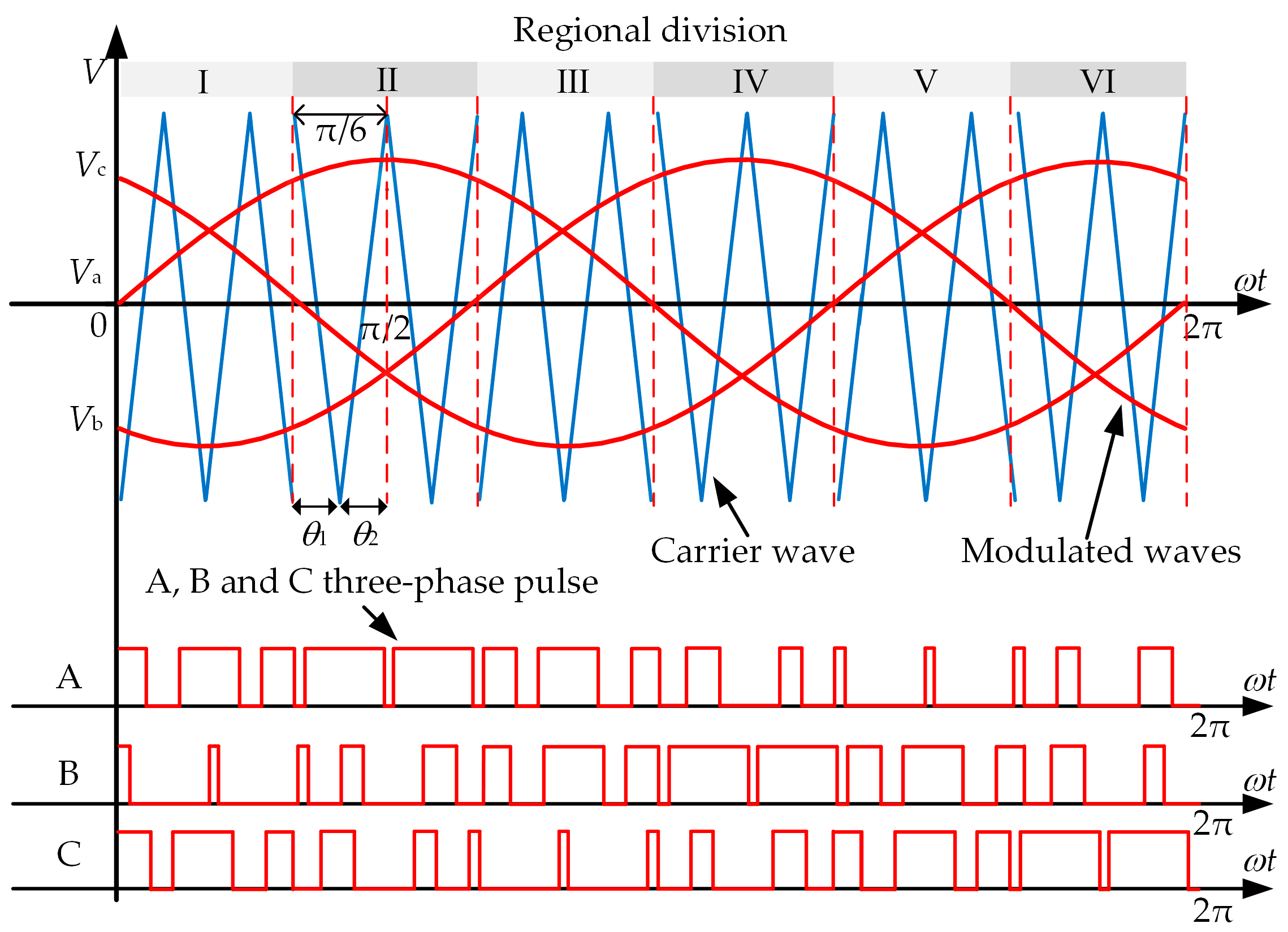
2.1. Basic Principle of Synchronous Space Vector Modulation

The three-phase voltage inverter circuit topology is shown in Figure 1, with the three-phase bridge arms Sa, Sb, and Sc, respectively. The upper power device conduction is defined as one, and the lower power device conduction is defined as zero in the bridge arm of one phase. Then, according to the different switching states of the three-phase bridge arm power devices, eight basic voltage vectors can be generated, six valid and two zero. Moreover, according to the vector distribution, the complex plane is divided into six equal regions labeled as sectors 1~6, as shown in Figure 2.
The SSVM strategy equates the reference voltage through two neighboring effective vectors in each sector and two zero vectors. As shown in figure Vref, it is assumed that the reference voltage vector is at sector 1, which, according to the volt-second balance principle, yields:
T 1 = ( 2 3 / π ) m T s sin 60 ° θ T 2 = ( 2 3 / π ) m T s sin θ T z = T s T 1 T 2 ,
where T1, T2, and Tz denote the effective vector and zero vector actions in one cycle Ts, respectively. m is the modulation index, calculated as m =Vref/(2Vdc/π).
SSVM requires that its switching sequences all have the characteristics of half wave symmetry (HWS), quarter wave symmetry (QWS), and three-phase symmetries (TS). It is assumed that the reference voltage is in phase and lies in the range of sector 1. The states of the voltage phases under various symmetry conditions are provided in Table 1.

2.2. Space Vector Implementation and Carrier Wave Implementation Equivalence Principle

Space vector modulation (SVM) and sinusoidal pulse width modulation (SPWM) are not two independent modulation modes but are intrinsically related. SVM can be realized by adding different zero-sequence components to the SPWM sinusoidal modulation waveform equivalently, and the modulation waveform expression is:
V am = V m sin ω t + V 0 V bm = V m sin ω t 2 3 π + V 0 V cm = V m sin ω t + 2 3 π + V 0 ,
where Vam, Vbm, and Vcm are the three-phase modulated waves after adding the zero-sequence components, Vm is the initial modulated wave amplitude, V0 denotes the added zero-sequence components, and the range of values of the zero-sequence components is:
1 V min V 0 1 V max ,
where Vmax/min = max/min {Vam, Vbm, Vcm}. According to the range of zero-sequence components in Equation (3), the mean value of the extrema is selected as the zero-sequence component, and the expression of the zero-sequence component is:
V 0 = 1 2 V max + V min .
By injecting the zero-sequence component in the above equation into the SPWM modulated wave, it can achieve complete equivalence with SVM without complex operations such as trigonometric functions. The algorithm is simple and easy to implement. Based on this equivalence principle, this article optimizes the synchronous symmetric modulation strategy based on the carrier.

3. Optimized Discontinuous Carrier Pulse Width Modulation

Based on the improved modulating waveform based on the conventional SCBDPWM, this article proposes to design an optimized pulse width modulation strategy based on the discontinuous carrier waveform by optimizing the carrier waveform. Compared with the space vector-based modulation strategy, the modulation strategy realized by equivalently comparing the modulating waveform with the carrier waveform is more straightforward. It can effectively reduce the voltage harmonic distortion rate and realize the optimization of the inverter output waveform quality.

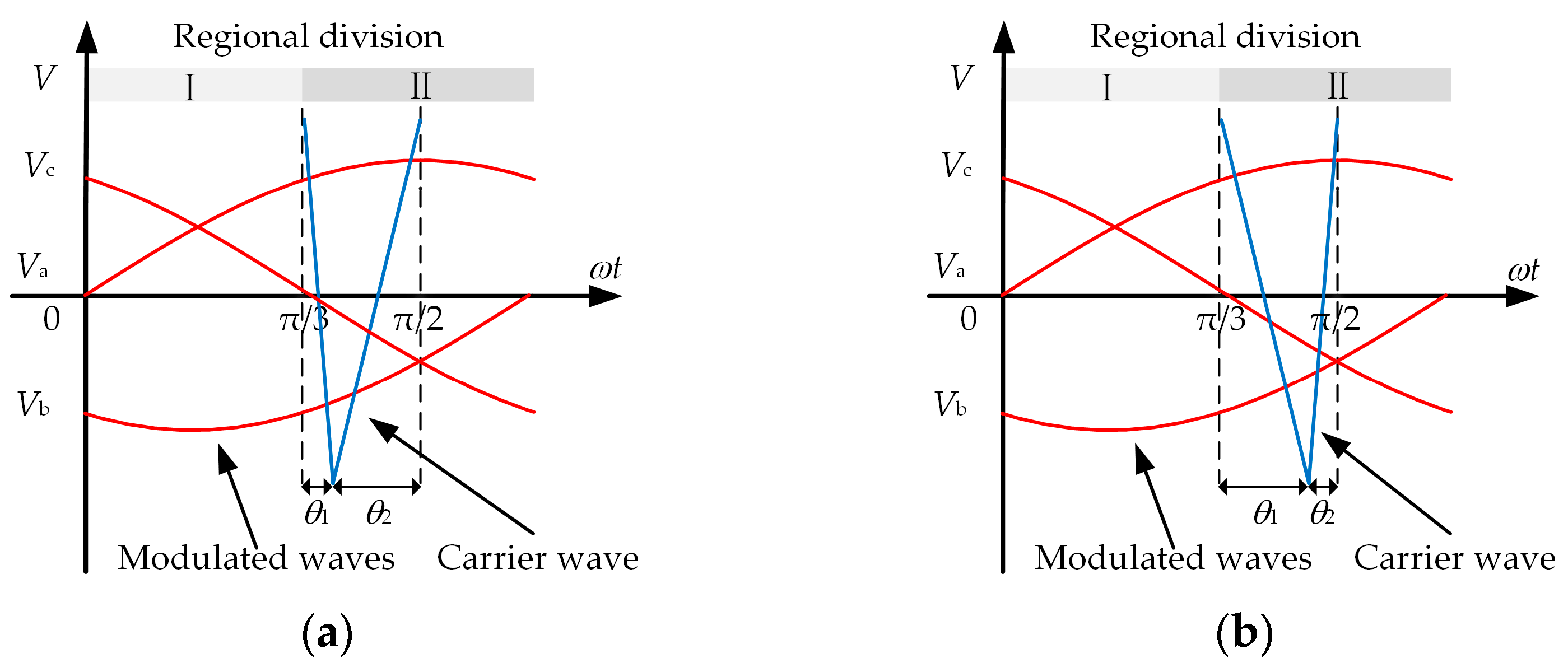
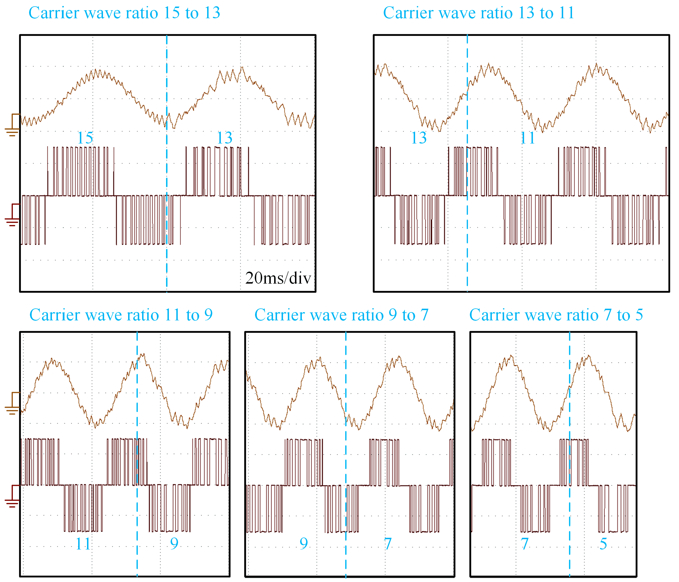
3.1. ODCPWM Strategy Design Principle

To optimize the output waveform quality of the inverter and reduce the switching frequency of the power device, the modulation strategy design of the three-phase voltage source inverter should meet the following conditions: TS, HWS, and QWS to avoid even harmonics and triple harmonics and minimize the adverse effects. Like the conventional SCBDPWM strategy, ODCPWM divides the region with a three-phase modulation wave in a fundamental wave period as an example under the premise of ensuring synchronous symmetry and carrying out carrier design. The three-phase modulated wave is divided into six regions I, II, …, VI inside a fundamental wave period, as shown in Figure 3. Taking the A phase voltage as an example, to satisfy the odd symmetry of HWS, I, II, III and VI, V, IV, only the region I, II, III or VI, V, IV should be considered when designing the carrier. To satisfy the TS, the adjacent area is odd symmetric, I, II, III, and only the II area should be considered when designing the carrier. To satisfy the QWS, zone II is symmetrical about the center (π/2), and only the first half of zone II (π/3 to π/2) is considered when designing the carrier. For the convenience of analysis, the range from π/3 to π/2 is defined as the carrier wave design region, and the width of the design region is π/6.
It is clear from the analysis above that to acquire the carrier for the entire fundamental wave period, only the carrier wave design in the carrier wave design zone needs to be considered. Therefore, when designing the discontinuous carriers in this article, the following principles should be followed:
  • The carrier wave is a peak or valley at the right edge (π/2) of the carrier design zone to satisfy the design requirement of carrier discontinuity.
  • The carrier is a peak or valley at the left edge (π/3) of the carrier design zone to satisfy the design requirement of carrier discontinuity.
  • To prevent the power devices of the two-phase bridge arms from activating simultaneously, which is against the inverter’s operating principle, the corresponding clamping mode of the modulating wave should also be considered while constructing the discontinuous carrier.
In this article, a specified zero-sequence frequency bias is added to the modulating waveform to produce either 30° or 60° voltage clamp mode.
The triangular carriers are continuous in each fundamental wave period of the conventional synchronous carrier modulation strategy, and the width of each triangular carrier in the fundamental wave period is the same. Therefore, this article optimizes the triangular carrier while satisfying the above design principles. N is the quantity of half-triangular carrier wave present in the designated carrier design zone. For instance, N = 1, 2 successively indicates the presence of a half-triangular carrier wave and a complete triangular carrier wave in the carrier wave design zone. Due to the limitation of a high-power inverter speed control system, the selected carrier wave ratio is often less than 15. Two angles are defined in the specified carrier design zone: θ1, θ2 (θ1 + θ2 = π/6), and the number of a half-triangular carrier wave in the angle occupied by θ1, θ2 is denoted by N1 and N2, N1 + N2 = N, and N1 and N2 are not simultaneously 0.
According to the different angles of θ1, θ2 and the different N1 and N2, the optimized discontinuous carriers are designed to satisfy the corresponding needs. Since all the discontinuous carrier waves designed according to the principles proposed in the article cannot be listed, they are illustrated below with N1 = N2 = 1. When θ1 = θ2, the carrier width in θ1 is consistent with that in θ2, defined as the ODCPWM-I. The carrier design is shown in Figure 3. When θ1 = 0.5θ2, the width of the carrier in θ1 is half of that in θ2, defined as the ODCPWM-II, and the carrier design is shown in Figure 4a. When θ1 = 2θ2, the width of the carrier in θ1 is twice that in θ2, and the carrier design is shown in Figure 4b, which is defined as the ODCPWM-III.
The following section describes the three ODCPWM-I/II/III.
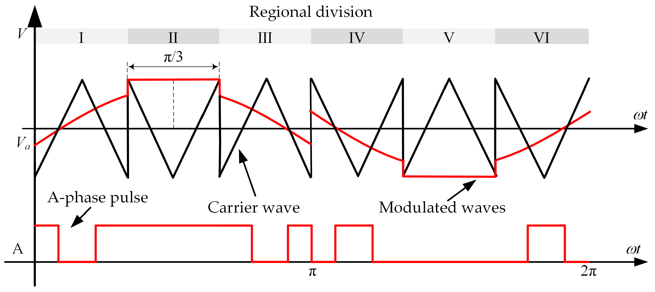
  • The ODCPWM-I is designed according to the above principles and is the same as conventional synchronous carrier modulation. In the ODCPWM-I, each carrier has the same width in any fundamental wave period. According to principles 1 and 2, the carriers wave in region II and region I are oddly symmetric, and the carriers jump at π/3.
  • Different modulation strategies can be obtained with different N and clamping methods according to the design principles. Some of the designs are summarized in Table 2. Table 2 shows that the possible carrier wave ratios chosen for the ODCPWM-I strategy are 5 and 7, defined as ODCPWM-I_5-I, ODCPWM-I_5-II, and ODCPWM-I_7. Take the ODCPWM-I_5-II strategy shown in Table 2 as an example. As shown in Figure 5, the A-phase voltage modulation wave in a fundamental wave period is compared with the carrier wave. The modulation wave in the II region is clamped to a higher level to ensure that design principle 3 is satisfied.
  • Unlike the above strategy, while satisfying the above design principles, ODCPWM-II has different carrier widths in each fundamental wave period. The angle occupied by the half-triangular carrier in the angular range of θ1 is one-half of the angle occupied by the half-triangular carrier in the angular range of θ2 in the specified carrier design zone. At this time, the carrier with a larger angle near the π/2 position and the triangular carrier with a smaller angle near the π/3 position exists in region II.
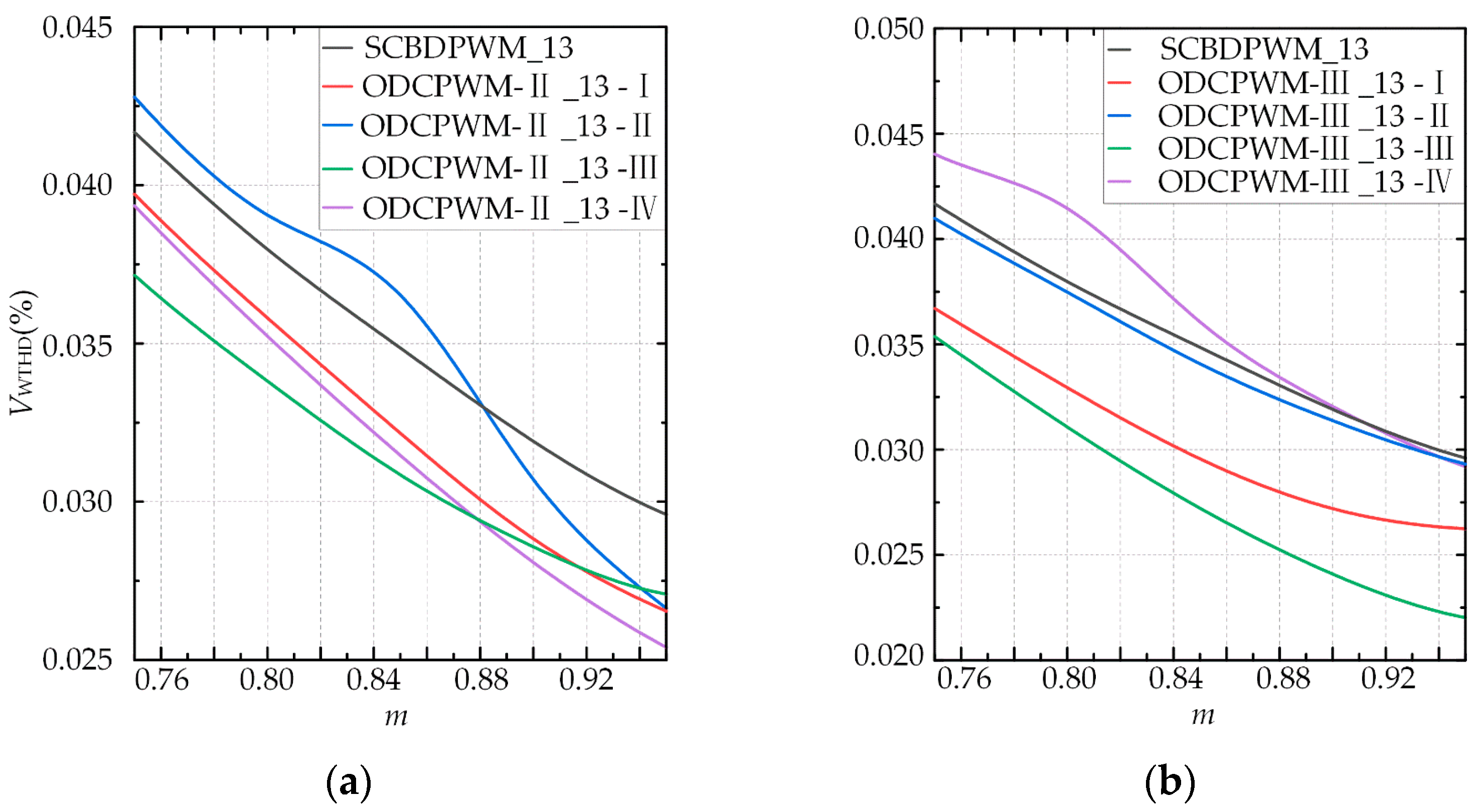
  • Following the above principles for ODCPWM-II, various optimized discontinuous pulse width modulation strategies that satisfy the design principles can be obtained, and some of the designs are summarized in Table 3. The carrier wave ratios that may be selected for the ODCPWM-II are 7 and 13, defined as ODCPWM-II_7 and ODCPWM-II_13-I/II/III/IV, respectively, taking ODCPWM-II_13-III shown in Table 3 as an example. The modulating waveform is compared with the carrier waveform, as shown in Figure 6. Each π/6 is clamped in regions I and III to ensure that design principle 3 is satisfied.
  • Similar to the above ODCPWM-II, the carrier width differs in each fundamental wave period in ODCPWM-III. In this strategy, the angle occupied by the half-triangular carrier in the angular range of θ1 is twice the angle occupied by the half-triangular carrier in the angular range of θ2. At this time, there exists a half-triangular carrier with a smaller angle near the π/2 position and a half-triangular carrier with a larger angle near the π/3 position in region II.
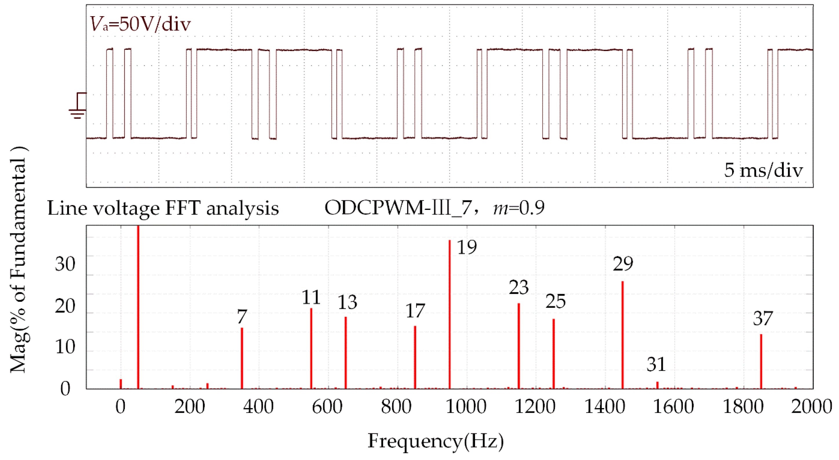
  • According to the above principle for ODCPWM-III design, the possible carrier wave ratios of the ODCPWM-III are 7 and 13 according to different clamping methods. They are defined as ODCPWM-III_7 and ODCPWM-III_13-I/II/III/IV, respectively, which are uniformly summarized in Table 4, taking the ODCPWM-III_7 shown in Table 4 as an example. The comparison of the A-phase voltage-modulated waveform and carrier waveform is shown in Figure 7. Each π/6 in regions I and III is clamped to ensure that design principle 3 is satisfied.

3.2. ODCPWM Modulation Strategy Performance

3.2.1. Performance Evaluation Index

In this section, the influence of different modulation strategies on performance is analyzed when the modulation index m is changed, and the carrier wave ratio is different.
At present, the widely used method to compare the quality of inverter output waveform under different modulation strategies is to compare the content of harmonic components other than the fundamental wave; that is, the distortion degree of output voltage waveform relative to the ideal sinusoidal waveform. The total harmonic distortion (THD) of the output voltage is defined as:
V THD = n = 2 V n V 1 2 , ( n 1 ) ,
where V1 and Vn are the effective values of the fundamental component and the nth harmonic component of the output voltage.
The lower the VTHD value, the higher the power factor in the whole system, the smaller the peak current, and the higher the efficiency. That is, the smaller the adverse effect of the inverter on the system. If the drive system is regarded as an inductive load, the higher the number of harmonics, the better the filtering effect after passing through the inductive load, and the smaller the impact on the drive system. Therefore, the influence of low-order harmonics on system loss and output torque is more significant than high-order harmonics. When the switching frequency is the same, the output voltage VTHD of most modulation strategies is not much different [20]. At this time, it is not appropriate to use the output voltage VTHD to characterize the quality of the output waveform. It is more reasonable to use the output voltage weighted total harmonic distortion VWTHD as an indicator to characterize the quality of the inverter output waveform, which is defined as follows:
V WTHD = n = 2 V n n 2 V 1 .

3.2.2. Optimal ODCPWM Strategy Selection

The lower the degree of harmonic distortion when different modulation methods are used with the same carrier wave ratio, the better the harmonic characteristics will be. Under the DC bus voltage Vdc = 150 V, fundamental frequency fe = 50 Hz, and the same switching frequency is observed. In the setting modulation range, the harmonic content of the proposed ODCPWM strategy and the conventional SCBDPWM strategy is compared by Matlab/Simulink simulation software. The results of the cross-sectional comparison of VWTHD in three groups are provided in this article.
Since the proposed strategy contains more cases with a carrier wave ratio of 13, the analysis first distinguishes them according to the design principles and then makes VWTHD judgments. The results corresponding to the comparison of VWTHD under the action of conventional SCBDPWM and the proposed ODCPWM-II and ODCPWM-III, respectively, are shown in Figure 8. It can be seen that the proposed strategy ODCPWM-II_13-II has a lower VWTHD compared to SCBDPWM_13 at a modulation index m ≥ 0.88 for a carrier wave ratio of 13 in Figure 8a. Moreover, ODCPWM-II_13-I, ODCPWM-II_13-III, and ODCPWM-II_13-IV have low VWTHD in the whole modulation index range m = 0.75~0.95. In Figure 8b, the proposed strategy ODCPWM-III_13-IV has a lower VWTHD than SCBDPWM_13 at m ≥ 0.91, while ODCPWM-III_13-I, ODCPWM-III_13-II, and ODCPWM-III_13-III also have a lower VWTHD than SCBDPWM_13 in the whole range. By comparing the overall strategies, it can be obtained that the ODCPWM-III_13-III strategy has the lowest VWTHD in this modulation index range. In other words, the inverter output waveform quality under this strategy is optimal.
At the carrier wave ratio 7, the results corresponding to the comparison of VWTHD under the action of SCBDPWM and the proposed ODCPWM-I/II/III/IV are shown in Figure 9a. The proposed ODCPWM-I/II/III/IV_7 has a low VWTHD in the whole range of modulation index m = 0.75~0.95, with ODCPWM-III_7 having the best performance. At carrier wave ratio 5, the proposed ODCPWM-I_5 strategy has a lower VWTHD at m ≥ 0.92, as shown in Figure 9b.

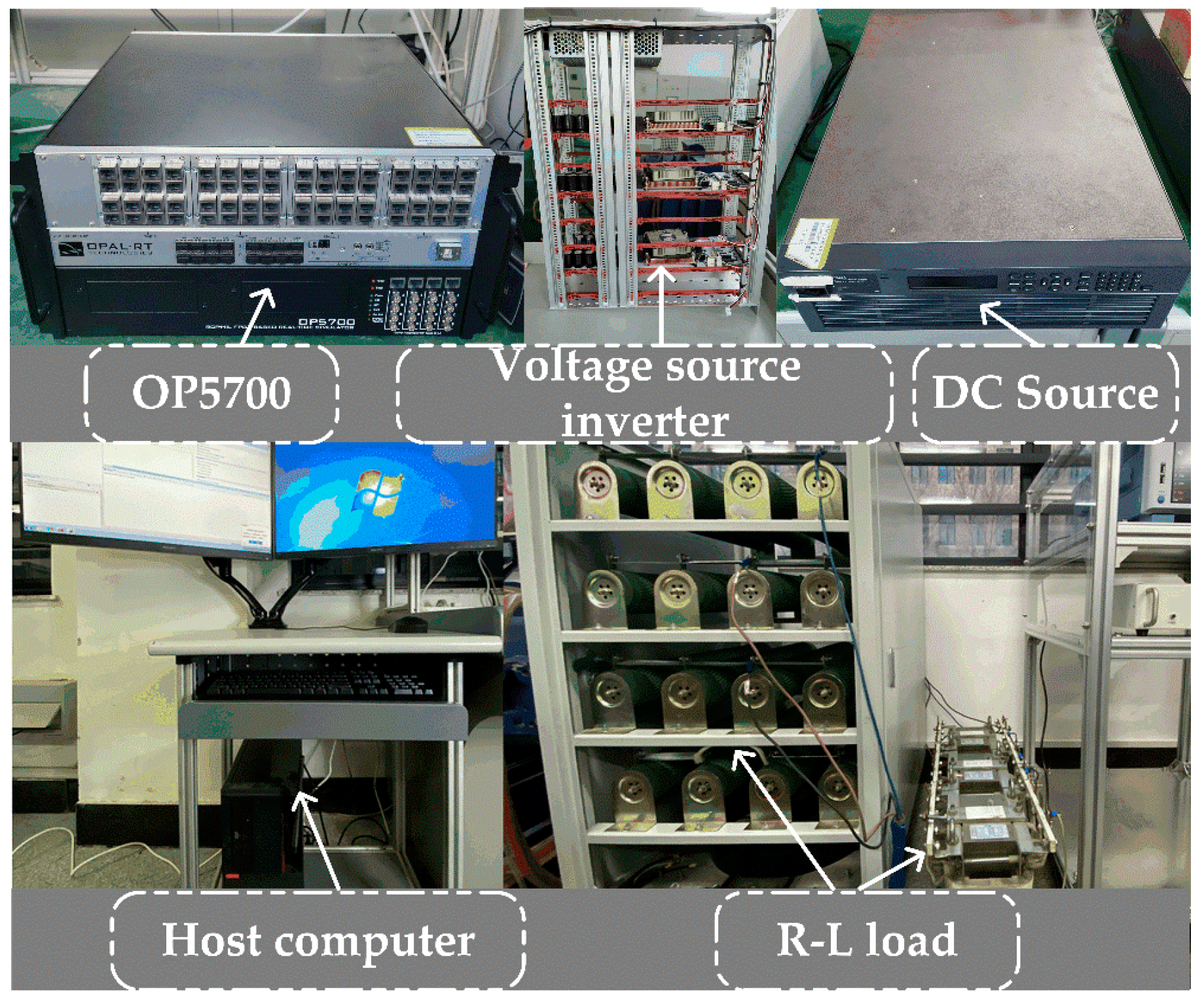
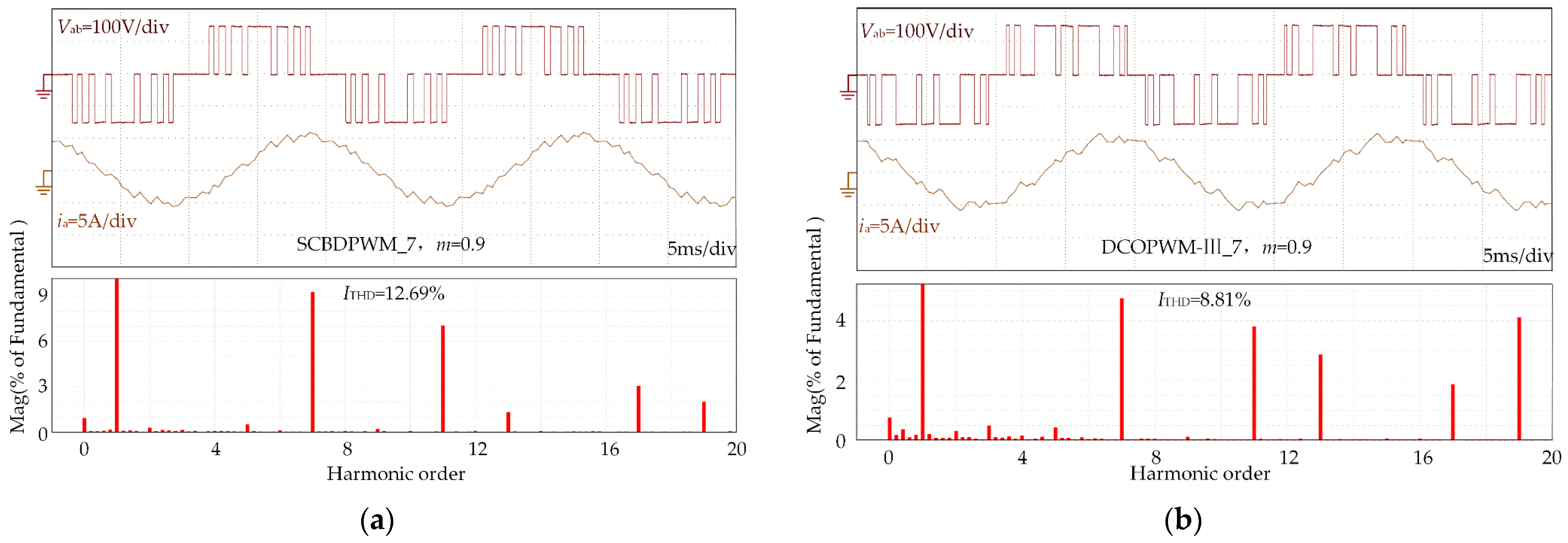
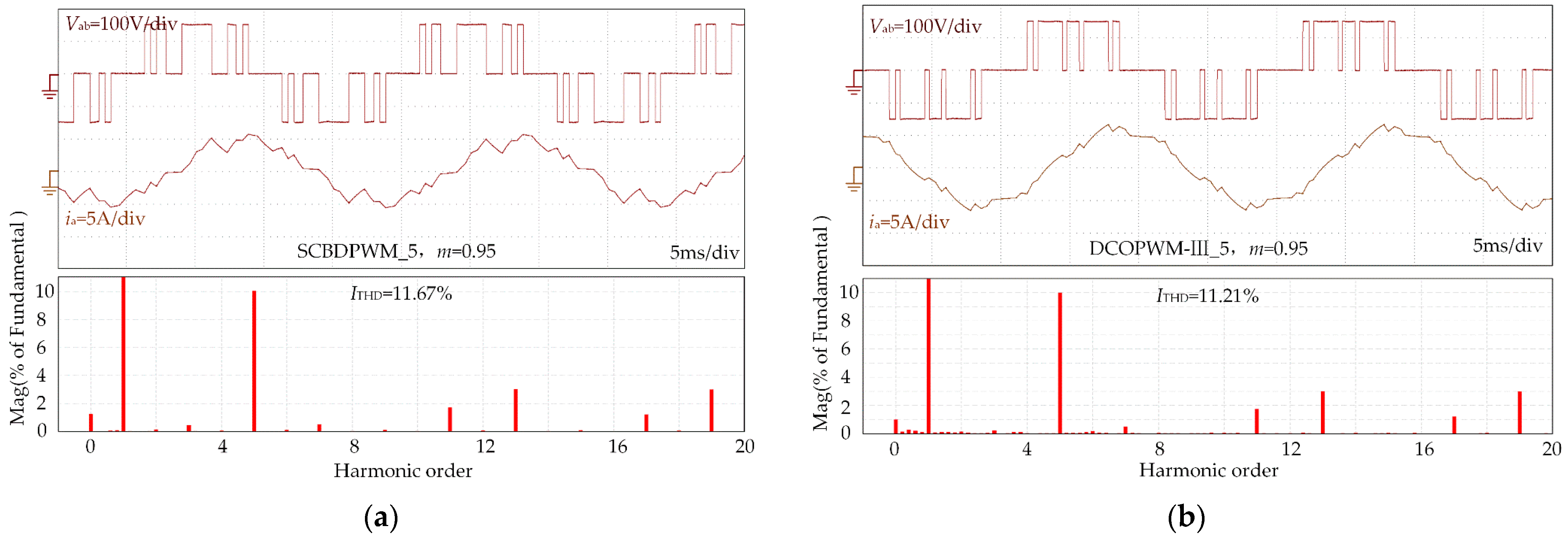
4. Experimental Verification

In order to verify the feasibility and effectiveness of the proposed ODCPWM strategy, the rapid control prototype OP5700 (OPAL-RT Co. Ltd., Richardson, Montreal, QC, Canada) and the SIC unit module PEB8024 (Imperix Co. Ltd., Sion, Switzerland) are adopted to establish the experimental setup, as shown in Figure 10.
The above experimental system compares the proposed optimized discontinuous carrier pulse width modulation with the conventional carrier-based discontinuous pulse width modulation strategy. The experimental parameters are set as shown in Table 5.
From Figure 11, Figure 12 and Figure 13, it can be seen that the voltage waveforms under the effect of the optimized discontinuous carrier pulse width modulation are all in line with the half-wave odd symmetry and 1/4 period even symmetry. There is no even harmonic and triple harmonic distribution, which can prove that the proposed ODCPWM can optimize the voltage harmonic performance to a certain extent.
Since the system control accuracy is directly affected when the inverter output current has significant harmonics, total current harmonic distortion is used to evaluate the output current waveform quality of the inverter when comparing various control strategies and is defined as:
I THD = n = 2 I n 2 I 1 ,
where I1 is the fundamental frequency RMS value of the output current and In is the RMS value of the nth harmonic component of the output current.
When the inverter drives the inductive load, the relationship between the nth harmonic component of the output voltage and the effective value of the nth harmonic component of the output current can be approximated as follows:
I n V n n ω L σ , n = 2 , 3 , 4 ,
where ω is the output fundamental frequency, and Lσ is the equivalent inductance. Substituting Formula (4) into Formula (3):
I THD n = 2 V n n ω L σ 2 I 1 = n = 2 V n n 2 ω L σ I 1 ,
where I1 is proportional to V1, so ITHD is proportional to VWTHD. Therefore, for the inverter with a given reference voltage, the total harmonic distortion of the output current and the weighted total harmonic distortion of the output voltage can be regarded as equivalent. The difference is that ITHD depends on the system parameters, while VWTHD is unaffected by the system parameters. Since the current output harmonics will directly affect the system performance, the total harmonic distortion of the phase current is selected as the evaluation index in the experiment.
The comparison of the inverter output line voltage Vab, current ia waveforms, and current spectrum under the action of ODCPWM-I/II/III and conventional SCBDPWM with different carrier wave ratios (13, 7, 5) are shown in Figure 14, Figure 15 and Figure 16, respectively. It can be seen that when the modulation index is 0.9, the carrier wave ratio is 13 and 7, the modulation index is 0.95, the carrier wave ratio is 5, and the total harmonic distortion of the inverter output current under the optimization strategy ODCPWM-I/II/III is lower than that of the conventional SCBDPWM. As shown in Table 6, the total harmonic distortion of current under different modulation strategies is listed in the table for comparison, which can effectively prove the effectiveness of the improved strategy described in this article.
In addition, this article proposes an improved multi-mode pulse width modulation strategy based on ODCPWM for smooth operation in the whole speed range. When different carrier wave ratio switching is carried out, the three-phase switching state is required not to carry out switching action before and after switching at different carrier wave ratios to ensure that no shock is generated when switching and no significant abrupt change in the fundamental phase occurs. Thus, the basic principle of the switching phase described in this article is as follows: firstly, when switching at different carrier wave ratios, ensure that the A-phase switching state is constant and find the optimal switching point position of A-phase; secondly, according to the principle of ODCPWM-I/II/III designed in this article, the carrier is designed according to the principle of sector division, and the B-phase delays the A-phase by π/3 and the C-phase delays the B-phase by π/3, so that there is still no switching when ensuring the B-phase and C-phase switching. The switching between different carrier wave ratios is completed during half of the fundamental wave.
The results of an experiment on the inverter output voltage and current fluctuations using an optimized discontinuous carrier pulse width modulation technique are presented in Figure 17. The modulation index is increased, and the carrier wave ratio is switched from 15 to 5, resulting in frequency switching points of 33 Hz to 49 Hz. The multi-mode synchronous modulation strategy leads to optimal switching phase selection, and the results show a smooth switching process with no shock.

5. Conclusions

This article comprehensively analyzes a novel approach to PWM in voltage source inverters called optimized discontinuous carrier pulse width modulation (ODCPWM) to solve the problem of large output harmonic content of conventional carrier modulation strategy. The fundamental wave period is symmetrically divided according to TS, HWS, and QWS, and the carrier is flipped in adjacent regions. The carrier width is symmetrically changed in each region. By changing the number and width of carriers and matching with different voltage clamping methods, various ODCPWM are obtained. By comparing the VWTHD of each ODCPWM, the optimal ODCPWM of VWTHD under different carrier wave ratios is further obtained.
Secondly, a multi-mode PWM strategy in the whole speed range is designed based on the ODCPWM with the best performance at different carrier wave ratios proposed in this article. The switching process is analyzed from the perspective of selecting the best switching point position so that the fundamental wave periodic phase does not change abruptly before and after switching to achieve smooth switching.
Finally, the effectiveness of the proposed strategy is verified by experiments. Compared with the conventional SCBPWM, the ODCPWM proposed in this article can eliminate the even harmonics and three times harmonics in the line voltage harmonics. The VWTHD is lower, improving the output waveform’s quality and making the system more stable and reliable. In addition, each ODCPWM directly compares the modulation wave with the optimized carrier to obtain the switching signal of each power device, which is simple in calculation and convenient in implementation. According to the method proposed in this article, the multi-mode PWM strategy is switched. There is no current shock during the switching process, and smooth switching between different carrier wave ratios can be achieved, which performs better in the whole speed range.

Author Contributions

Formal analysis, X.J. and W.C.; Funding acquisition, W.C. and T.S.; Methodology, X.J. and J.L.; Project administration, W.C. and T.S.; Validation, X.J. and J.L.; Writing—original draft, J.L.; Writing—review and editing, W.C. All authors will be informed about each step of manuscript processing including submission, revision, revision reminder, etc. via emails from our system or assigned Assistant Editor. All authors have read and agreed to the published version of the manuscript.

Funding

This research was funded by the National Natural Science Foundation of China, grant number 52077156; the Key Program of Tianjin Natural Science Foundation, grant number 20JCZDJC00020.

Data Availability Statement

The data presented in this study are available on request from the corresponding author. The data are not publicly available due to privacy.

Conflicts of Interest

The authors declare no conflict of interest. The funders had no role in the design of the study; in the collection, analyses, or interpretation of data; in the writing of the manuscript; or in the decision to publish the results.

References

  1. Renz, E.C.; Turso, J. Toward the Application of Pulse Width Modulated (PWM) Inverter Drive-Based Electric Propulsion to Ice Capable Ships. Energies 2022, 15, 8217. [Google Scholar] [CrossRef]
  2. Xiao, L.; Li, J.; Xiong, Y.; Chen, J.; Gao, H. Strategy and Implementation of Harmonic-Reduced Synchronized SVPWM for High-Power Traction Machine Drives. IEEE Trans. Power Electron. 2020, 35, 5472–5481. [Google Scholar] [CrossRef]
  3. Jammala, V.; Yellasiri, S.; Panda, A.K. Development of a New Hybrid Multilevel Inverter Using Modified Carrier SPWM Switching Strategy. IEEE Trans. Power Electron. 2018, 33, 8192–8197. [Google Scholar] [CrossRef]
  4. Vasantharaj, S.; Indragandhi, V.; Bharathidasan, M.; Aljafari, B. Power Quality Analysis of a Hybrid Microgrid-Based SVM Inverter-Fed Induction Motor Drive with Modulation Index Diversification. Energies 2022, 15, 7916. [Google Scholar] [CrossRef]
  5. Almazán-Covarrubias, J.H.; Peraza-Vázquez, H.; Peña-Delgado, A.F.; García-Vite, P.M. An Improved Dingo Optimization Algorithm Applied to SHE-PWM Modulation Strategy. Appl. Sci. 2022, 12, 992. [Google Scholar] [CrossRef]
  6. Birda, A.; Reuss, J.; Hackl, C.M. Synchronous Optimal Pulse Width Modulation for Synchronous Machines with Highly Operating Point Dependent Magnetic Anisotropy. IEEE Trans. Ind. Electron. 2021, 68, 3760–3769. [Google Scholar] [CrossRef]
  7. Li, K.; Yuan, Q.; Nai, W. Model Prediction and Pulse Optimal Modulation of Electrically Excited Synchronous Motor at Low Switching Frequency. Electronics 2022, 11, 1173. [Google Scholar] [CrossRef]
  8. Busacca, A.; Di Tommaso, A.O.; Miceli, R.; Nevoloso, C.; Schettino, G.; Scaglione, G.; Viola, F.; Colak, I. Switching Frequency Effects on the Efficiency and Harmonic Distortion in a Three-Phase Five-Level CHBMI Prototype with Multicarrier PWM Schemes: Experimental Analysis. Energies 2022, 15, 586. [Google Scholar] [CrossRef]
  9. Janabi, A.; Wang, B. Hybrid SVPWM Scheme to Minimize the Common-Mode Voltage Frequency and Amplitude in Voltage Source Inverter Drives. IEEE Trans. Power Electron. 2019, 34, 1595–1610. [Google Scholar] [CrossRef]
  10. Riedemann, J.; Zhu, Z.; Stone, D.; Foster, M.; Greenough, J.; Takemoto, K.; Ivanovic, D.; Bateman, B. A Space Vector Modulation Strategy for PMSMs Operating at Low Switching-to-Fundamental Frequency Ratio. IEEE Trans. Ind. Electron. 2022, 99, 1–10. [Google Scholar]
  11. Gao, Z.; Ge, Q.; Li, Y.; Zhao, L.; Zhang, B.; Wang, K. Hybrid Improved Carrier-Based PWM Strategy for Three-Level Neutral-Point-Clamped Inverter with Wide Frequency Range. IEEE Trans. Power Electron. 2021, 36, 8517–8538. [Google Scholar] [CrossRef]
  12. Xu, J.; Soeiro, T.B.; Wu, Y.; Gao, F.; Wang, Y.; Tang, H.; Bauer, P. A Carrier-Based Two-Phase-Clamped DPWM Strategy With Zero-Sequence Voltage Injection for Three-Phase Quasi-Two-Stage Buck-Type Rectifiers. IEEE Trans. Power Electron. 2022, 37, 5196–5211. [Google Scholar] [CrossRef]
  13. Beig, A.R.; Kanukollu, S.; Al Hosani, K.; Dekka, A. Space-vector-based synchronized three-level discontinuous PWM for medium-voltage high-power VSI. IEEE Trans. Power Electron. 2014, 61, 3891–3901. [Google Scholar] [CrossRef]
  14. Fernandez-Gomez, M.; Sanchez, A.; de Castro, A.; Lopez-Lopez, J.; Zumel, P.; Fernandez, C. Design and Implementation of Two Hybrid High Frequency DPWMs Using Delay Blocks on FPGAs. IEEE Trans. Power Electron. 2021, 36, 14567–14578. [Google Scholar] [CrossRef]
  15. Tcai, A.; Alsofyani, I.M.; Seo, I.-Y.; Lee, K.-B. DC-link Ripple Reduction in a DPWM-Based Two-Level VSI. Energies 2018, 11, 3008. [Google Scholar] [CrossRef] [Green Version]
  16. Zhang, Z.; Li, B.; Zhang, G.; Wang, G.; Huang, Z.; Hu, B.; Long, T.; Xu, D. Optimized Carrier-Based DPWM Strategy Adopting Self-Adjusted Redundant Clamping Modes for Vienna Rectifiers With Unbalanced DC Links. IEEE Trans. Power Electron. 2023, 38, 1622–1634. [Google Scholar] [CrossRef]
  17. Lawan, M.G.; Camara, M.B.; Sabr, A.S.; Dakyo, B.; Al Ameri, A. Power Control Strategy for Hybrid System Using Three-Level Converters for an Insulated Micro-Grid System Application. Processes 2022, 10, 2539. [Google Scholar] [CrossRef]
  18. Lee, H.-J.; Yoo, A.; Hong, C.; Lee, J. A carrier-based adjustable discontinuous PWM for three-phase voltage source inverter. In Proceedings of the 2015 IEEE Energy Conversion Congress and Exposition (ECCE), Montreal, QC, Canada, 20–24 September 2015; pp. 2870–2875. [Google Scholar]
  19. Kohlhepp, B.; Duerbaum, T. Novel DPWM Modulation Scheme for Three-Phase ZVS Inverters. In Proceedings of the 2021 56th International Universities Power Engineering Conference (UPEC), Middlesbrough, UK, 31 August–3 September 2021; pp. 1–6. [Google Scholar]
  20. El Gadari, A.; El Ouardi, H.; Ounejjar, Y.; Al-Haddad, K. Novel Three-Phase Nine-Level Inverter and Its Control Strategies. Electronics 2022, 11, 3348. [Google Scholar] [CrossRef]
Figure 1. Three-phase voltage inverter.
Energies 16 02401 g001
Figure 2. Basic voltage vector diagram.
Energies 16 02401 g002
Figure 3. Three-phase modulation wave region division and output pulse.
Energies 16 02401 g003
Figure 4. Carrier design with different modulation strategies: (a) ODCPWM-II modulation strategy; (b) ODCPWM-III modulation strategy.
Energies 16 02401 g004
Figure 5. Comparison of modulating waveform and carrier waveform and pulse waveform in ODCPWM-I_5-II.
Energies 16 02401 g005
Figure 6. Comparison of modulating waveform and carrier waveform and pulse waveform in ODCPWM-II_13-III.
Energies 16 02401 g006
Figure 7. Comparison of modulating waveform and carrier waveform and pulse waveform in ODCPWM-III_7.
Energies 16 02401 g007
Figure 8. VWTHD with different modulation strategies at carrier wave ratio of 13: (a) Comparison of SCBDPWM modulation strategy and ODCPWM-II modulation strategy; (b) comparison of SCBDPWM modulation strategy and ODCPWM-III modulation strategy.
Energies 16 02401 g008
Figure 9. VWTHD with different modulation strategies: (a) Comparison of different modulation strategies at carrier wave ratio 7; (b) comparison of different modulation strategies at carrier wave ratio 5.
Energies 16 02401 g009
Figure 10. The prototype of OPAL-RT company ROP5700 driven two-level inverter.
Energies 16 02401 g010
Figure 11. Harmonic analysis of phase voltage and line voltage at carrier wave ratio 13.
Energies 16 02401 g011
Figure 12. Harmonic analysis of phase voltage and line voltage at carrier wave ratio 7.
Energies 16 02401 g012
Figure 13. Harmonic analysis of phase voltage and line voltage at carrier wave ratio 5.
Energies 16 02401 g013
Figure 14. Line voltage waveform and phase current waveform at carrier wave ratio 13: (a) SCBDPWM modulation strategies; (b) ODCPWM-III_13-III modulation strategies.
Energies 16 02401 g014
Figure 15. Line voltage waveform and phase current waveform at carrier wave ratio 7: (a) SCBDPWM modulation strategies; (b) ODCPWM-III_7 modulation strategies.
Energies 16 02401 g015
Figure 16. Line voltage waveform and phase current waveform at carrier wave ratio 5: (a) SCBDPWM modulation strategies; (b) ODCPWM-III_5 modulation strategies.
Energies 16 02401 g016
Figure 17. Line voltage and current waveforms at switching time of multi-mode modulation.
Energies 16 02401 g017
Table 1. Inverter switching state phase relationship.
θθ ± 2πθ + 2/3πθ ± ππ − θ
V0(000)V0(000)V0(000)V7(111)V0(000)
V7(111)V7(111)V7(111)V0(000)V7(111)
V1(100)V1(100)V3(010)V4(011)V1(100)
V2(110)V2(110)V4(011)V5(001)V2(110)
Table 2. Partial implementation of each ODCPWM-I.
Carrier Wave RatioOptimization StrategyNClamping Methodπ/2 Moment Carrier Position
5ODCPWM-I_5-IN = 130°1
ODCPWM-I_5-IIN = 160°−1
7ODCPWM-I_7N = 230°−1
Table 3. Partial implementation of each ODCPWM-II.
Carrier Wave RatioOptimization Strategyθ1, θ2N1, N2Clamping MethodΠ/2 Moment Carrier Position
7ODCPWM-II_710°, 20°N1 = 1, N2 = 130°−1
13ODCPWM-II_13-I15°, 15°N1 = 2, N2 = 130°1
ODCPWM-II_13-II15°, 15°N1 = 2, N2 = 160°−1
ODCPWM-II_13-III6°, 24°N1 = 1, N2 = 230°1
ODCPWM-II_13-IV6°, 24°N1 = 1, N2 = 260°−1
Table 4. Partial implementation of each ODCPWM-III.
Carrier Wave RatioOptimization Strategyθ1, θ2N1, N2Clamping Methodπ/2 Moment Carrier Position
7ODCPWM-III_720°, 10°N1 = 1, N2 = 130°−1
13ODCPWM-III_13-I24°, 6°N1 = 2, N2 = 130°1
ODCPWM-III_13-II24°, 6°N1 = 2, N2 = 160°−1
ODCPWM-III_13-III15°, 15°N1 = 1, N2 = 230°1
ODCPWM-III_13-IV15°, 15°N1 = 1, N2 = 260°−1
Table 5. Experimental system parameters.
System ParametersSymbolsValues
DC-link voltageVdc150 V
DC-link capacitanceC1 C2780 μF
Load resistanceR10 Ω
Load inductanceL20 mH
Rated frequencyfe50 Hz
Table 6. Different modulation strategies in terms of ITHD.
Carrier Wave Ratios 13
m = 0.9
Carrier Wave Ratios 7
m = 0.9
Carrier Wave Ratios 5
m = 0.9
modulation strategyITHDmodulation strategyITHDmodulation strategyITHD
SCBDPWM8.01%SCBDPWM12.69%SCBDPWM11.67%
ODCPWM-III_13-III6.70%ODCPWM-III_78.81%ODCPWM-III_511.21%
Disclaimer/Publisher’s Note: The statements, opinions and data contained in all publications are solely those of the individual author(s) and contributor(s) and not of MDPI and/or the editor(s). MDPI and/or the editor(s) disclaim responsibility for any injury to people or property resulting from any ideas, methods, instructions or products referred to in the content.

