Article

Simulation of Series Resistance Increase through Solder Layer Cracking in Si Solar Cells under Thermal Cycling

Department of Mechanical Engineering, The State University of New York, Korea (SUNY Korea), Incheon 21985, Republic of Korea
Energies 2023, 16(6), 2524; https://doi.org/10.3390/en16062524
Submission received: 7 February 2023 / Revised: 2 March 2023 / Accepted: 6 March 2023 / Published: 7 March 2023

Abstract

:
In solar cell modules, thermal cycling stresses can cause cracking in the ribbon wire, leading to an increase in series resistance and a drop in the power output of the module. Quantitative analysis was conducted to study the increase in series resistance, considering two cracking models: continuous and random. In the continuous model, it was expected that if all the ribbon wires on the front side of the module cracked, the current would decrease linearly from 0 to 100%, and the series resistance would increase exponentially to infinity. In the random crack model, the current dropped slowly, and the series resistance increased less compared with that in the continuous one. A mathematical model based on the bypass mechanism of the currents was proposed to explain the differences between the two models. The study found that cracking in the solder layer under thermal cycling can be described by a combination of continuous and random models, which can represent the upper and lower levels of the series resistance increase. When the solar cell power dropped to 80%, the increase in series resistance was expected to be in the range of 200 to 250% using the continuous and random models, respectively.

1. Introduction

The construction of Si solar modules typically starts with a layer of low-iron tempered glass, followed by an ethylene-vinyl acetate (EVA) layer that acts as an adhesive and encapsulant. The Si wafer, which is responsible for generating electric currents from sunlight, is located beneath the EVA layer, and another layer of EVA is applied on top of it. Finally, there is a back sheet layer that provides structural support and protection. To transfer the electric currents generated in the Si wafer to other wafers, the module is equipped with several attached Cu ribbon wires. These ribbon wires are connected to the Si wafer using solder layers, which are coated onto the ribbon wires. The solder layers provide both electrical and mechanical connections between the ribbon wires and the Si wafer, ensuring reliable and efficient energy transfer.
The temperature difference between day and night or between summer and winter causes thermal cycling (TC) stress in outdoor solar modules. TC is known to be a detrimental stress that induces degradation of power conversion efficiency [1]. TC causes cracking of the solder layer due to the difference in the coefficient of thermal expansion between the materials. These cracks, in turn, increase the series resistance ( R s ) in the solar cell, leading to a reduction in power output. Many studies have identified this power degradation mechanism as a result of TC in solar cells [2,3,4,5,6]. As the power drop under TC is a function of an increase in  R s  in solar cells, it is important to know the quantitative relationship between the amounts of solder layer cracking and the increase in  R s , and the maximum  R s  increase allowed in a cell.
These concerns can be investigated numerically. Any numerical approach capable of Poisson’s equation and continuity equation for electrons and holes can simulate the solar cell’s electric behavior [7]. Analyses based on the finite element method (FEM) have been conducted in many studies. Malm and Edoff [8] studied the effects of bandgap energy and trap density of thin-film solar cells on the open-circuit voltage using a commercial FE package in a 2D model. To simulate the efficiency of the composition grading of thin-film solar cells, Brown et al. [9] solved the Poisson and continuity equations using a commercial FEM package. Shiradkar et al. [10] evaluated the leakage current under high potential in solar modules using a 2D FE model. Recently, using a designated solar cell simulator based on the 2D FEM, Asadpour et al. [11,12] studied the effect of solder bond failure in Si solar cells on current–voltage (I–V) curves. As processing both the Poisson and continuity equations simultaneously requires large amounts of computing resources, most studies have been limited to 1D or 2D FEMs for a partial area of a solar cell.
However, the current in solar cells flows through a 3D structure consisting of front ribbon wire, front electrode, wafer, rear electrode, and rear ribbon wire. Quantitative studies on the effect of solder layer cracking on  R s  increase in a cell require 3D full modeling of solar cells for numerical simulation. In this study, the continuity equation was separated from the Poisson’s equation by modeling the absorber layer of a Si solar cell in an equivalent resistance, and an electrostatic model for the entire solar cell in 3D FEM was constructed for the analysis of  R s  in Section 2. Next, cracking in the solder layer of the ribbon wire in a solar cell was reflected in the model, and the electric potential and current were analyzed to estimate the  R s  increase in the solar cell in Section 3. Extensive quantitative studies have been conducted on the effects of solder cracking associated with variations in the amount, position, front and rear, and pattern of cracking. The analysis results revealed a relationship between solder cracking and an increase in  R s . The flow of simulation conducted in this study is summarized in Figure 1 for clarity.

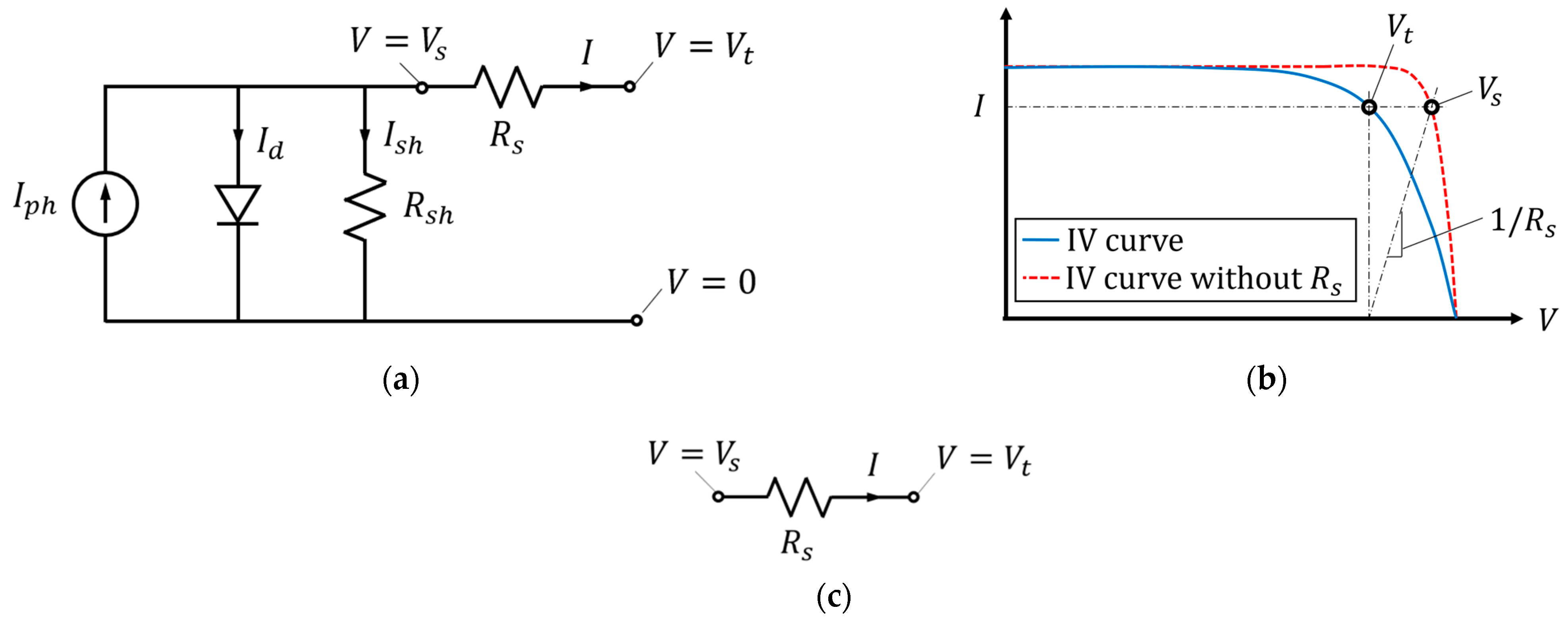
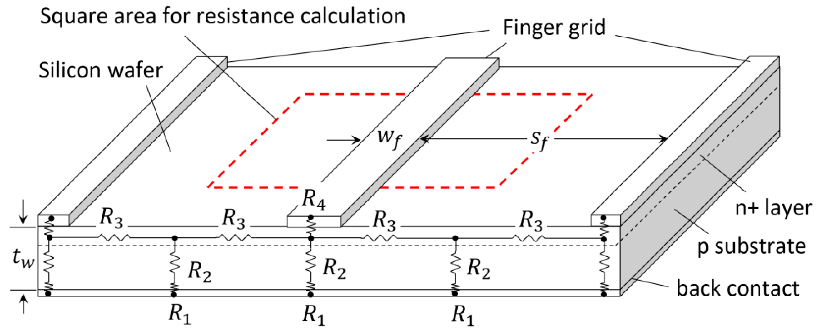
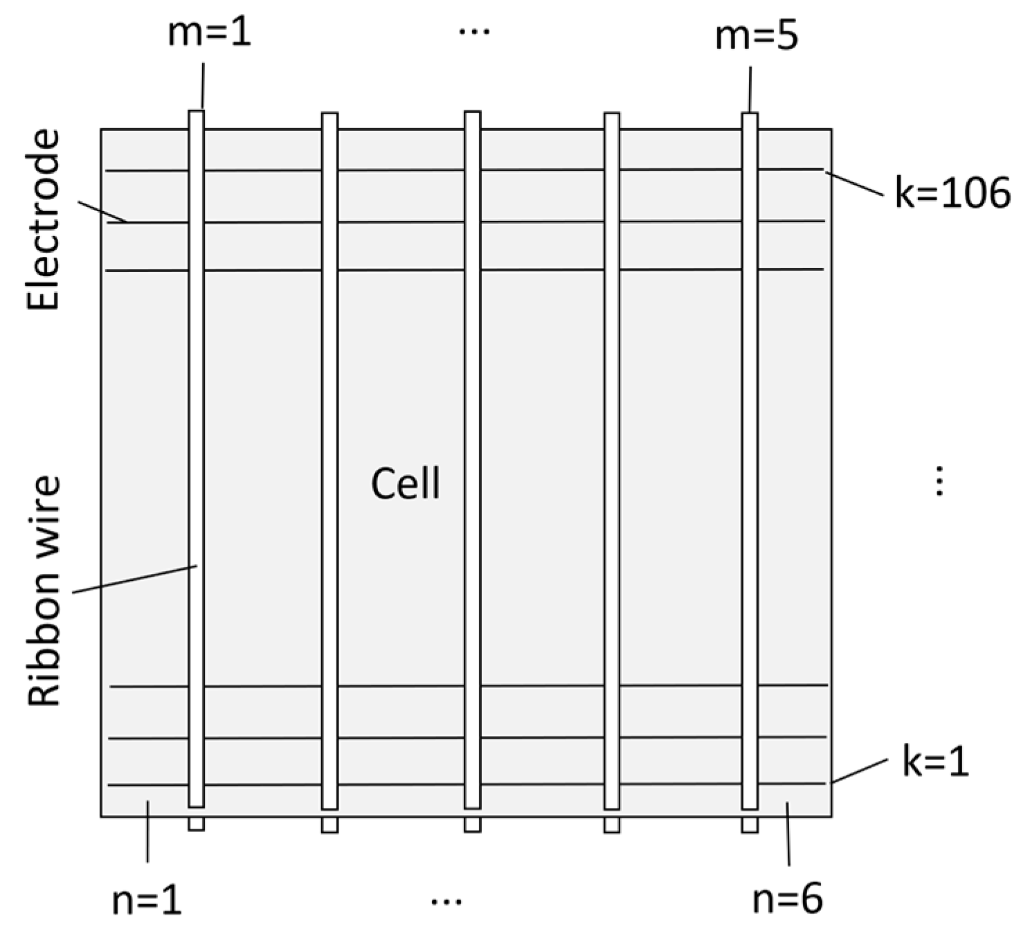
2. Simulation of Series Resistance in Solar Cells

In the equivalent circuit of the solar cell shown in Figure 2a, the current flow is expressed as:
I = I ph I d I sh = I ph I 0 [ exp ( V t + R s I aV T ) 1 ] V t + R s I R sh
In the equation,  R s  is caused by the resistance through the emitter and base of the solar cell, contact resistance between the metal contact and silicon, and resistance of the top and rear metals. The circuit can be defined by the voltages before and after  R s  as:
R s = V s V t I
where  V s  is as defined in Figure 2. To measure  R s , we need to monitor  V s . It can be interpreted that we need to measure the I–V curve of a solar cell without the  R s ,  as shown in Figure 2b, which is practically impossible.
However, this is possible in the simulations. If we model the solar cell by counting all the  R s  components and separating them from the current of photogeneration ( I ph ), diode effect ( I d ), and shunt resistance effect ( I sh ), as shown in Figure 2c, the  R s  can be estimated in an electrostatic problem.

2.1. Electrostatic Modeling Theory in FEM

In electrostatic problems, the Maxwell equations for materials are decoupled into electric and magnetic field pairs of equations. For electric field intensity  E , the Maxwell equations become:
· ε E = ρ
× E = 0
where  ρ  is the electric charge density and  ε  is the permittivity of the material [13]. Using the relation between the electric field intensity and potential,  E = V , Equation (3) is transformed into the Poisson’s equation as follows:
· ε V = ρ .
It becomes the Laplace’s equation for a free net charge situation,  ρ = 0 ,
· ε V = 0 .
For solar modules, a free net charge situation can be assumed except in the depletion region [14].
The solution to Equation (6) can be obtained through the FE analysis. In the FEM, the electric potential becomes:
V = { N } T { V e }
where  { N }  is the element shape function vector and  { V e }  is the nodal electric scalar potential vector. After applying the variational principle, the matrix equation for an electrostatic problem using a current-based electric element, such as SOLID231 in the commercial FE package ANSYS, ref. [15] becomes
[ K ] { V e } = { I e }
and
[ K ] = vol ( { N } T ) T [ σ ] ( { N } T ) T d ( vol )
where vol is the element volume,  [ σ ]  is the conductivity matrix, and  { I e }  is the nodal current vector.

2.2. Electrostatic Material Properties of Solar Cells

The constructed 3D FE model of the solar cell used for electrostatic analysis is shown in Figure 3. The model consists of a Si wafer, front Ag electrodes, back Al electrodes, Cu ribbon wires, and solder layers. It represents a real size of the solar cell of 155 × 158 mm2 with the thickness of 0.17 mm. It is composed of five bus bars of width 1 mm and 106 lines of front metal electrodes with a width of 0.1 mm. The spans of the bus bars and electrode are 30 mm and 1.4 mm, respectively. The element Solid231 was used in the ANSYS software. Through a convergence check, the number of nodes in the model was determined to be 7,904,195. Five ribbon wires (RW), consisting of a Cu layer and solder layer, are located at the busbar positions. They are denoted as RW1 to RW5 from left to right, as shown in Figure 3.
The required material property for the electrostatic analysis of Equation (6) is the conductivity or its inverse, resistivity. The adopted resistivities in the analysis are summarized in Table 1 for the solder, copper, silver, aluminum, and Si wafer. For Si wafers, there are three components of resistivity: bulk resistivity, emitter sheet resistance, and contact resistance.
The resistance of the Si wafer is defined at four points, as shown in Figure 4, where  w f s f , and  t w  are the finger grid width, span, and wafer thickness, respectively. In this study, typical dimensions of solar cells with  w f =  0.1,  s f =  1.4, and  t w =  0.17 mm were employed. The lower contact resistance between the wafer and back contact,  R 1 , is generally negligible [22]. The substrate resistance  R 2  is determined using the bulk resistivity [20]. Emitter resistance  R 3  is one of the main contributors and is determined using the emitter sheet resistance. The upper contact resistance between the wafer and finger  R 4  is determined using the contact resistance. For the dashed square area by  w f + s f  and wafer thickness  t w  shown in Figure 4, the calculations are as follows:
R 2 = ρ b × 2 t w / ( w f + s f ) 2 = 4.5   Ω ,
R 3 = R ES × ( s f / 2 ) / ( w f + s f ) = 25.7   Ω ,
R 4 = ρ c / ( w f × ( w f + s f ) ) = 2.0   Ω .
The total resistance in the longest pass of current is  R 2 + R 3 + R 4 =  32.2 Ω, and in the shortest pass is  R 2 + R 4 =  6.5 Ω. In the passes, the equivalent resistivity can be determined as:
ρ eq = ( R 2 + R 3 + R 4 ) × ( w f + s f ) 2 / 2 t w   = 213   Ω - mm .
ρ eq = ( R 2 + R 4 ) × ( w f + s f ) w f / t w   = 43   Ω - mm .
The average of them is 128 Ω-mm, which is the value of Si wafer equivalent resistivity in this study. Note that this is an overestimation, because the current tends to find the smallest resistance path.
The applied boundary conditions on the model were the electric potentials at the end of the RWs, as shown in Figure 5, where the normalized electric potentials, or ‘0′ and ‘1′ voltages, were applied.

2.3. Series Resistance Calculation

The electric potential plots of the cells obtained from the analysis are shown in Figure 6. The potential on the busbar of the front side was maintained as ‘1’, as shown in the details of Figure 6a. It drops sharply to ‘0′ at the front and rear sides of the cell.
To calculate the  R s  of the cell, the electric flow should also be considered. The electric current densities in the x- and y-directions are shown in Figure 7. In the x-direction, the current flow at the electrodes is dominant, as shown in Figure 7a. In the y-direction, the flow in the busbars prevails, as shown in Figure 7b. Interpreting the plots reveals the current flow in the cell as represented in Figure 7c. The current started to flow from the top of the five front busbars, divided into the front electrodes, and was distributed into the cell. At the rear side of the cell, the reverse motion of the current flow is expected; cell, electrode, and busbars. The amount of current flowing across the solar cell can be calculated by summing up the amount of the current at the ends of five busbars. When ‘1′ voltage was applied, the total amount of current was 179.4 A. The calculated  R s  of the cell was 1/179.4, or 0.0056 Ω.
It is known that typical values for area-normalized  R s  of Si solar cells are between 0.5 Ω-cm2 for laboratory-type solar cells and up to 1.3 Ω-cm2 for commercial solar cells [23]. In this study, they were found to be between 0.002 Ω and 0.005 Ω. Considering the overestimation of Si wafer equivalent resistivity, it can be said that the value of 0.0056 Ω from the analysis is in the correct estimation range.

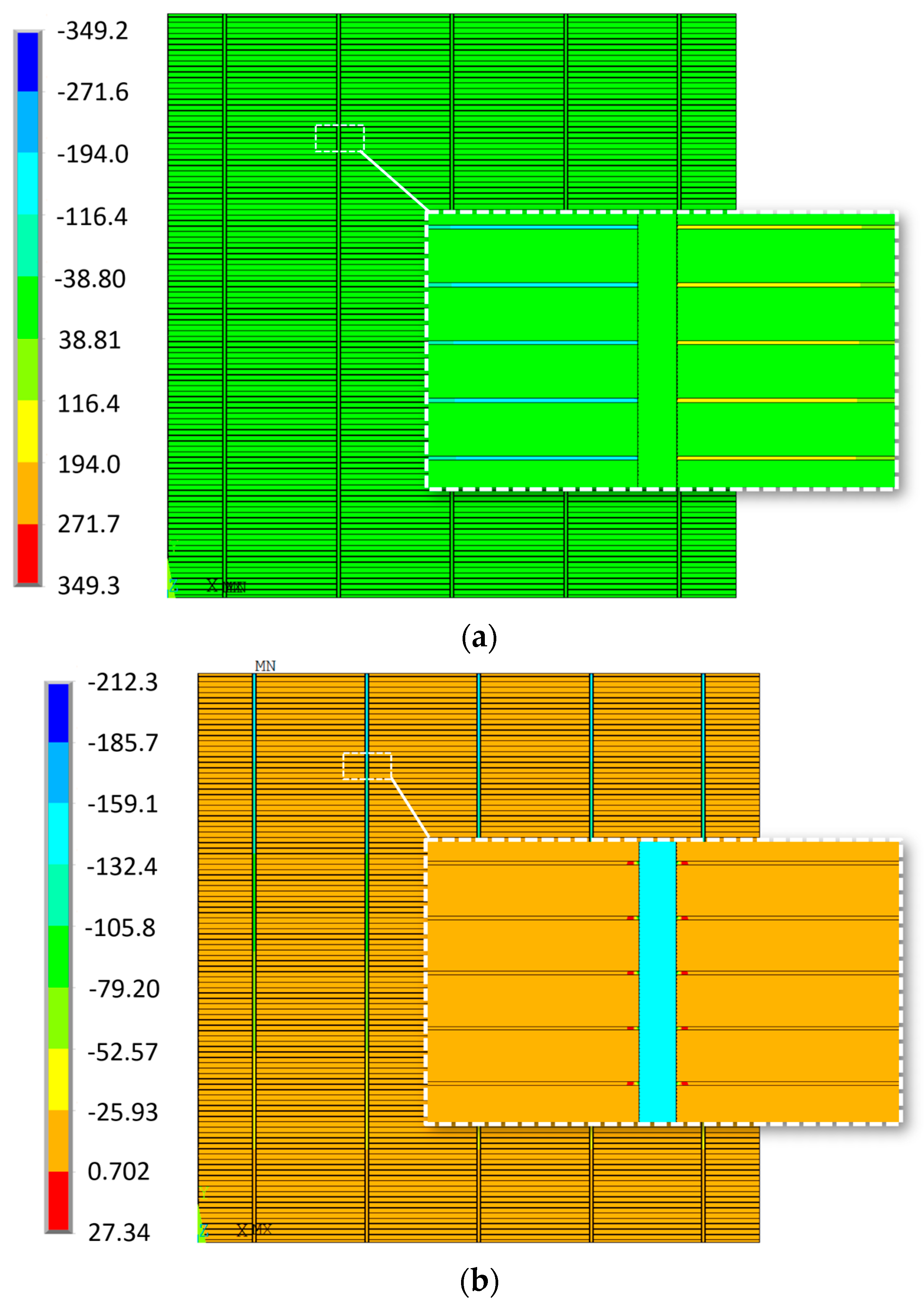
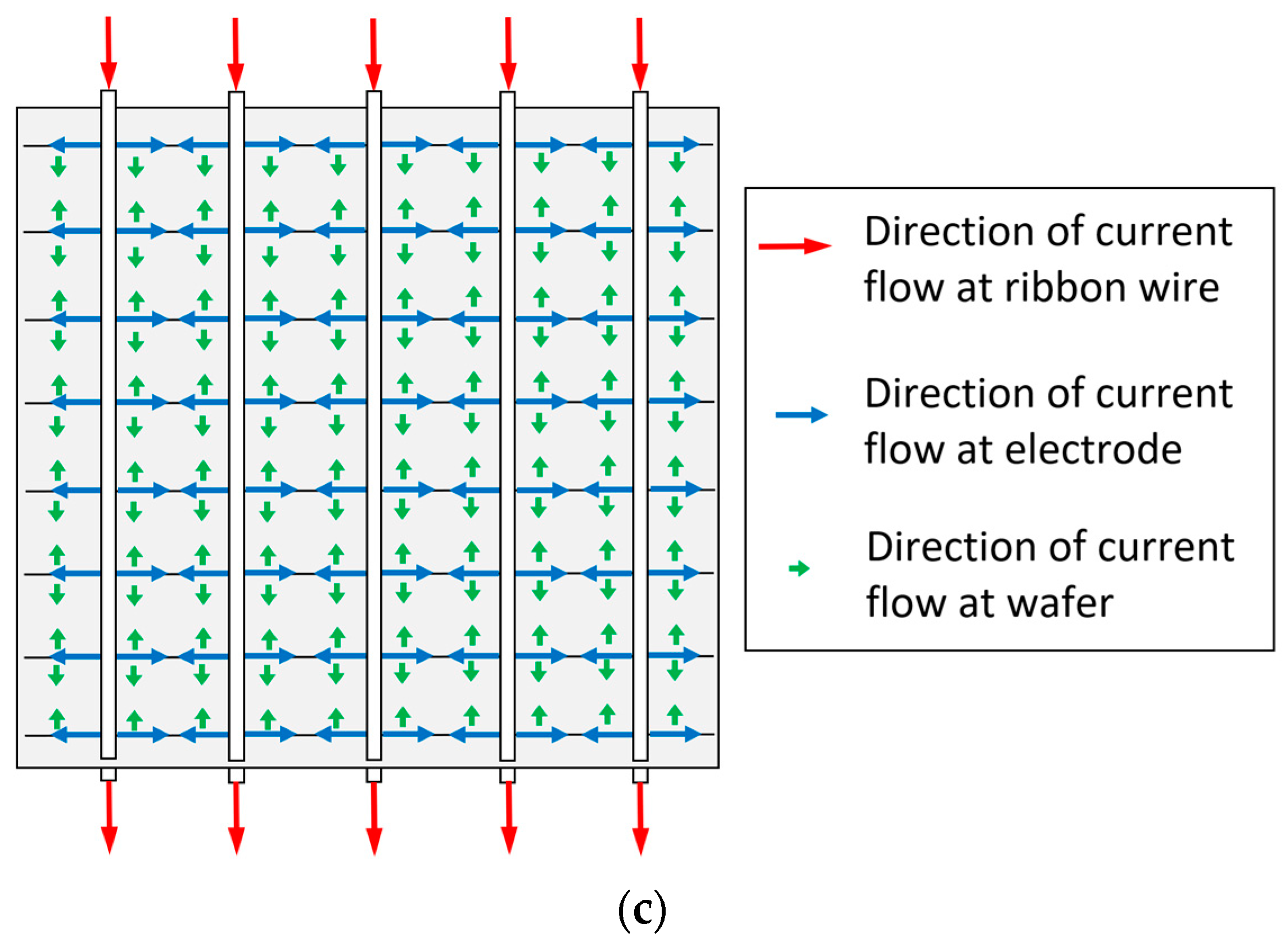
3. Simulation of Series Resistance Increase through Solder Layer Cracking

As shown in Figure 8, the cracks generated in the solder layer under TC stresses were modeled by removing the corresponding elements at the FE model previously configured. Many cases are possible with variations in the locations, sides, and amount of cracking. The simulated cases are summarized in Table 2. In the table, Case 0 corresponds to cases without cracking. Cases F, R, and FR stand for the cases with cracking at the front, rear, and both sides RWs of solar cells, respectively. The second index in Table 1, or -1, -3, -123, -12345, and -rand, represent the cracking positions at RW1, RW3, RW1 to RW3, RW1 to RW5, and random, respectively. A total of 10 cracking cases were simulated. For all the cases, except for the random case (Case FR-rand), it was assumed that a crack in the solder layer was initiated at the bottom of the ribbon wire, where the strain energy density reached a maximum [24] and propagated continuously.

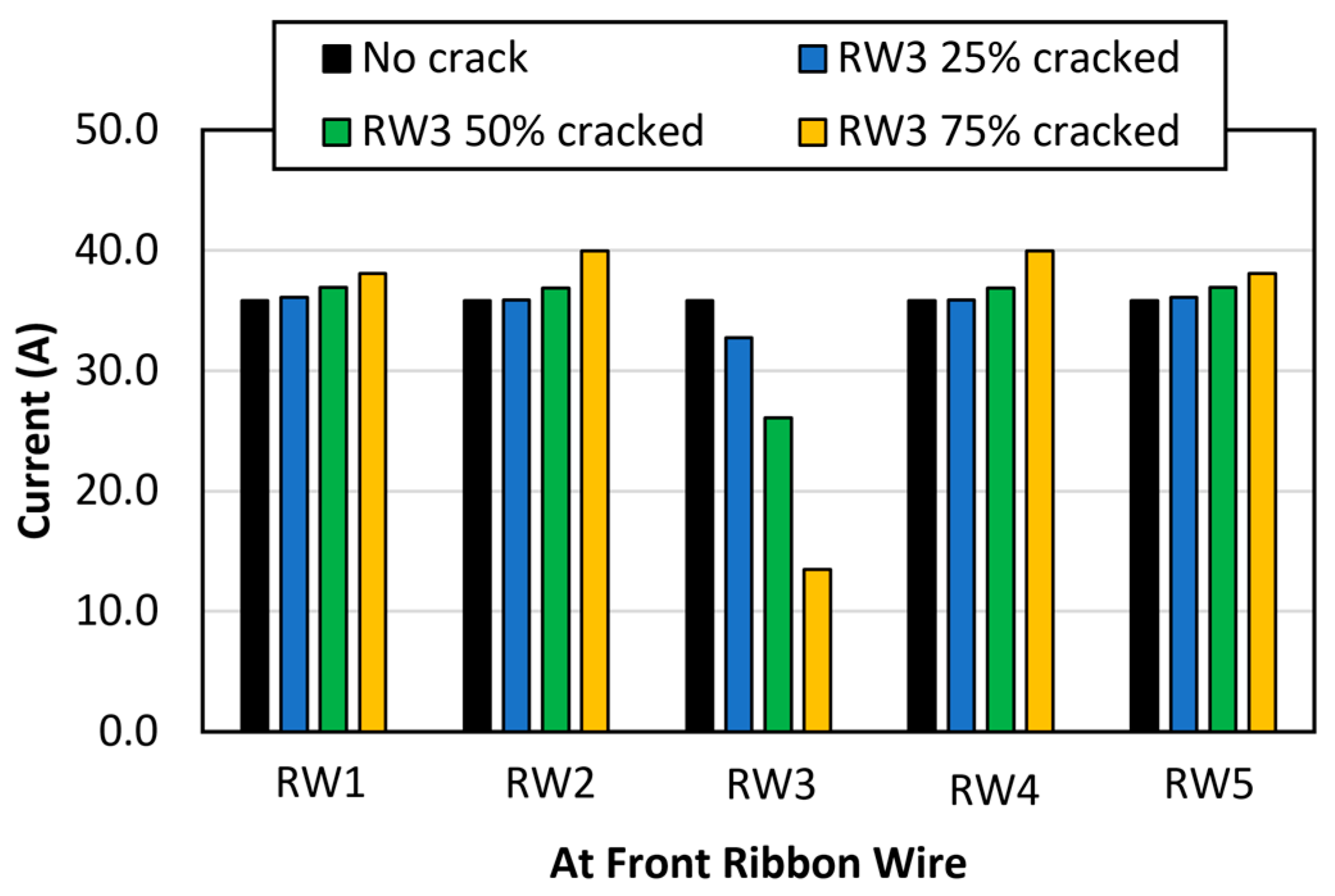
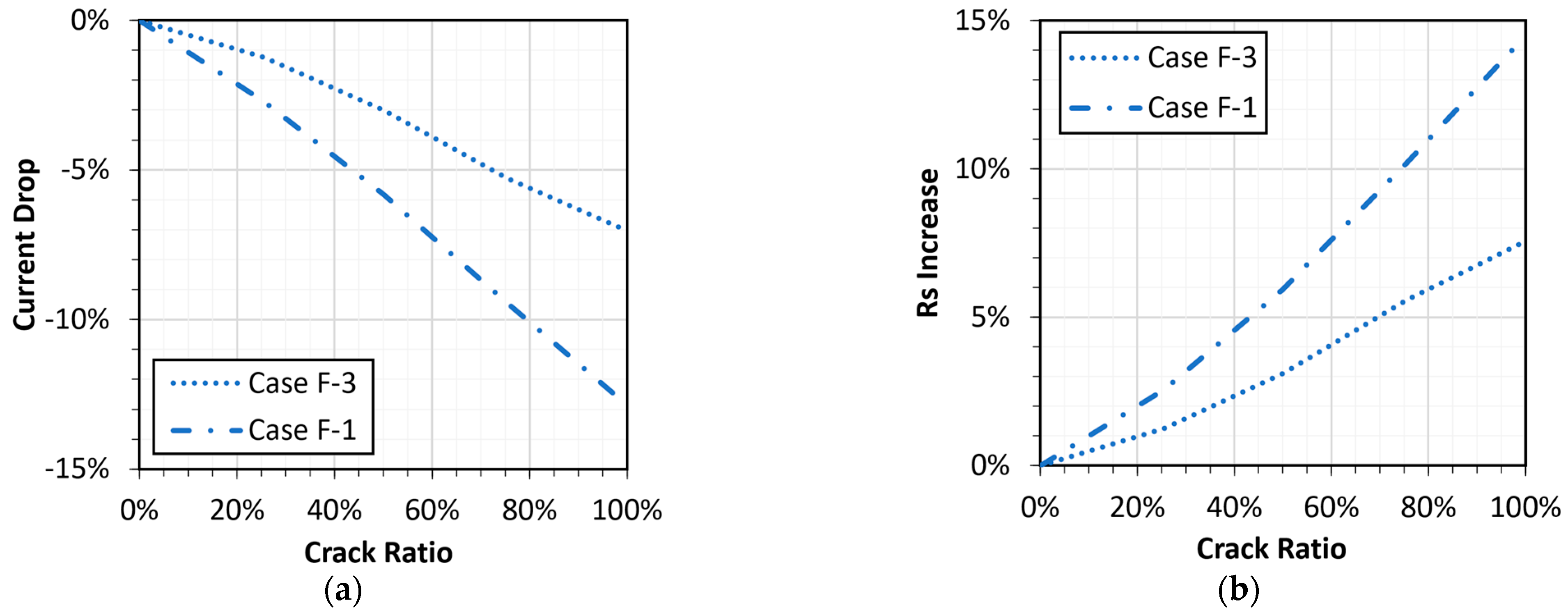
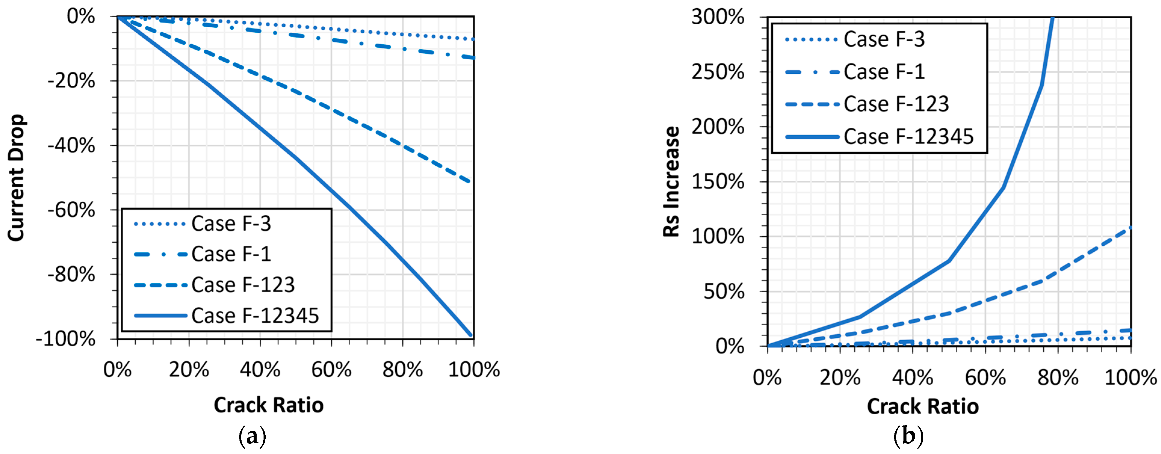
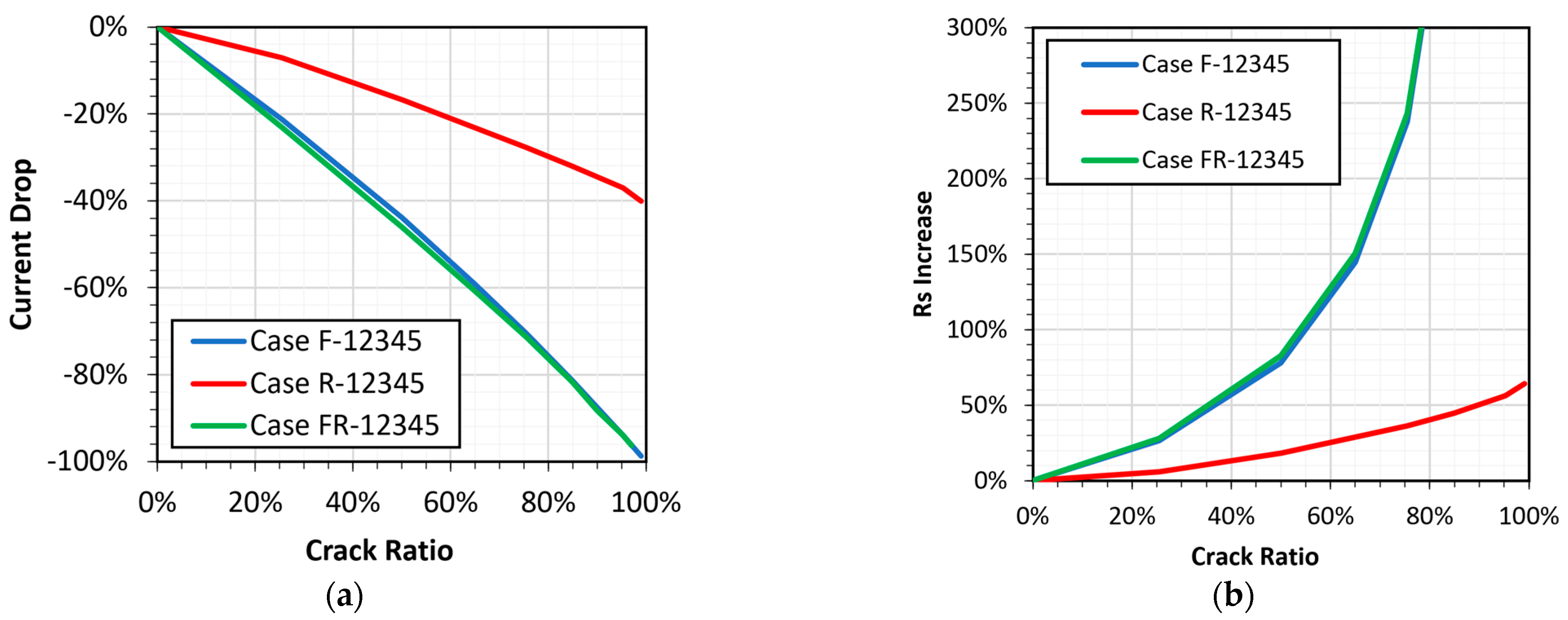
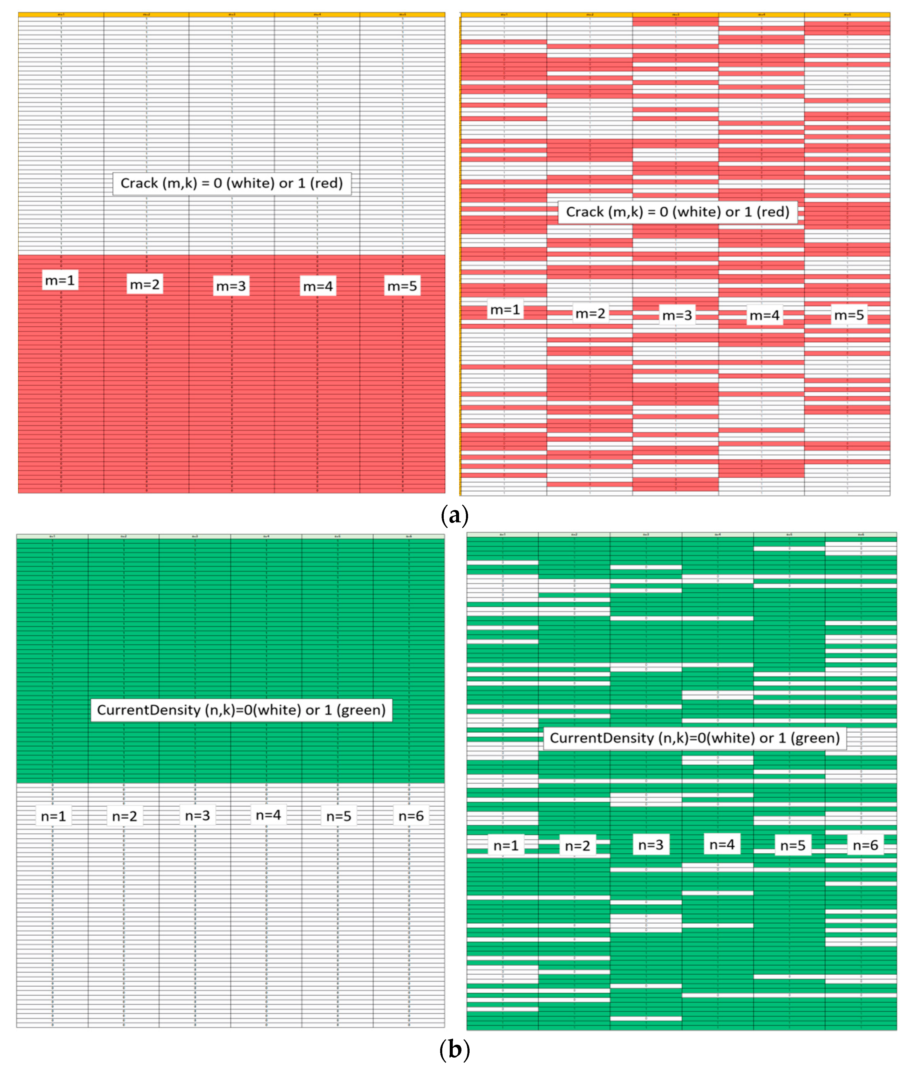
3.1. Cases with Continuous Cracks

When cracks were present in the solder layer, it was simulated that the electric potentials were broken by the cracks, and the currents stopped flowing in the areas, as shown in Figure 9. The results of the current stops for Case F-3 are depicted in Figure 10, which compares the change in the current output at the RWs when cracks propagate from 0 to 75% at RW3. The figure shows that the current at RW3 decreased as the crack propagated at RW3. Furthermore, it can be said that part of the lost current was compensated at the other RWs by the potential bypass of the current; however, it was not fully filled up and caused an increase in  R s .
Figure 11 shows the simulation results of the current drop and  R s  increase over the crack ratio for Cases F-1 and F-3. When the cracks continuously propagated to 100% in the RWs,  R s  increased up to 7.5% and 15% for Cases F-1 and F-3, respectively. The difference between the cases can be explained by the possibility of current bypassing at the cracked RWs. If there is a crack in RW1, the currents can only be bypassed in the right direction because there is no RW on the left. However, if a crack occurs in RW3, the current can bypass in both directions.
When multiple RWs start to crack continuously at once, more current drops and  R s  increases are expected, as shown in Figure 12. In Case F-12345, or when all the RWs at the front side crack from bottom to top, it was expected that the current drops from 0 to 100%, linearly and  R s  increases exponentially to infinity. However, it was less than 250% until all the RWs cracked to 75%. In Case F-123, the maximum  R s  increase was only up to 100%.
If cracks occurred in the RWs at the rear side, it was observed that the current dropped less and consequently  R s  increased less compared to the case of cracking at the front side, as shown in Figure 13. As the rear electrode covered the entire cell area, unlike the front electrode, it was easier to secure an alternative pass of current during cracking. It was expected that  R s  would increase by only 70% even if all the RWs were almost cracked.
Figure 14 compares the results of Cases F, R, and FR when all the RWs cracked continuously from bottom to top. As expected from Figure 12 and Figure 13, smaller drops and increases were estimated in Case R than in Case F. Notably, the effect of rear-side cracking is insignificant when all the front and rear sides are assumed to have cracks. Case FR produced a similar amount at the curves as Case F.

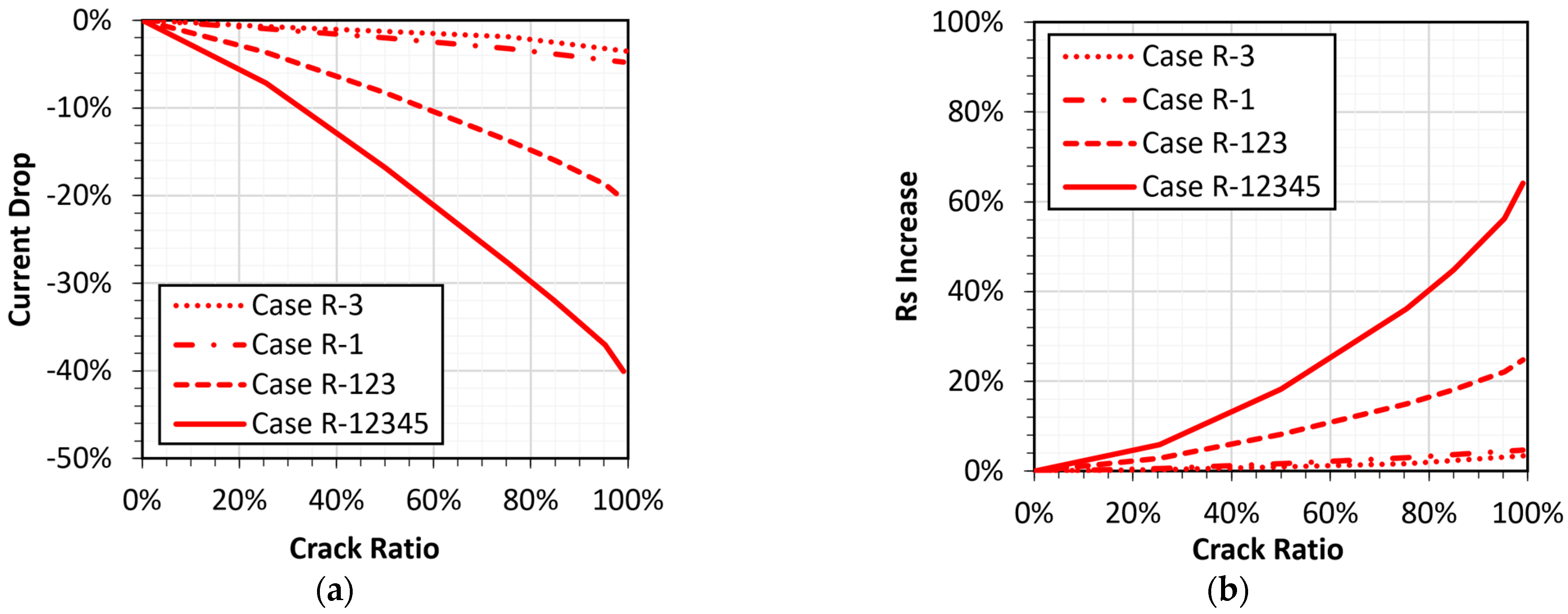
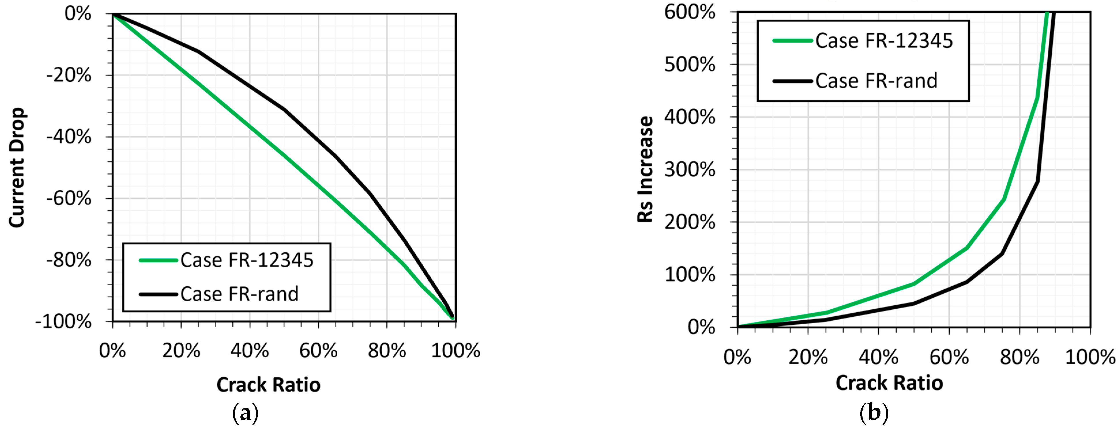
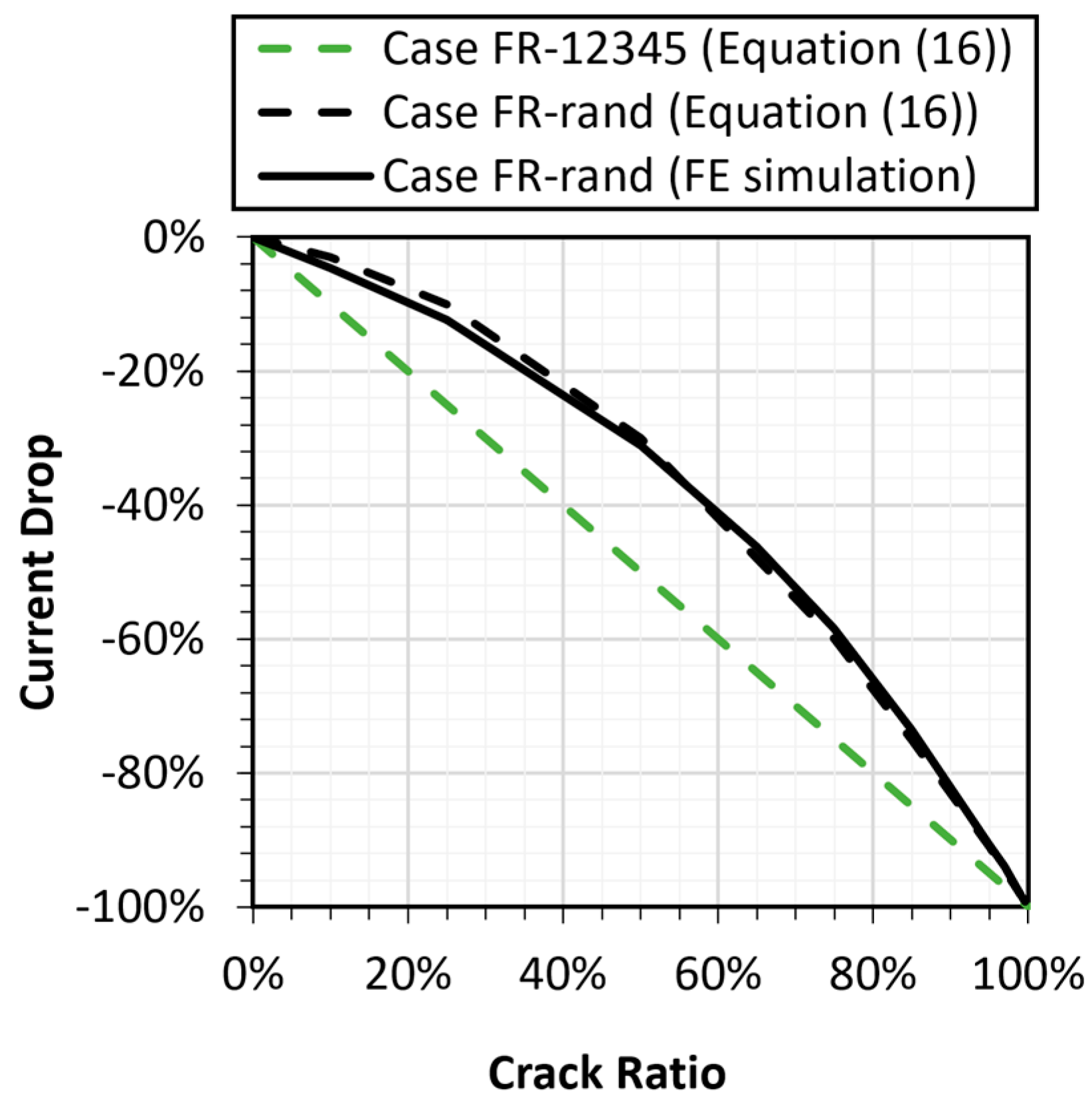
3.2. Case with Random Cracks

All the cases thus far have assumed that solder cracking starts at the bottom and propagates continuously to the top, based on an analysis of the maximum strain energy density position. However, cracks in the solder layer can be initiated at other positions or randomly. Case FR-rand simulates the random generation of cracks on both sides of the RWs. The results are presented in Figure 15. In the random case, the current dropped slowly, and the amount of  R s  increase reduced compared with that in Case FR-12345.  R s  was expected to increase to 45% and 200% when the solder layers were randomly cracked above 50% and 80%, respectively. In the case of continuous cracking,  R s  increased to 83% and 330% when the crack ratios were 50% and 80%, respectively.
A simple mathematical model can explain the difference between Cases FR-12345 and FR-rand. First, a crack function is defined, which indicates the status of cracking at solder layer positions m and k as follows:
Crack ( m , k ) = { 0 ,   cracked   1 ,   no   crack ,
where  m  is the number of ribbon wires (1–5 in this study) and  k  is the number of electrodes (1–106 in this study). In Case FR-12345, Equation (15) is zero from the bottom to the value defined by the crack ratio. In Case FR-rand, it will be zero at random, and the number of zeros will be determined by the crack ratio.
Next, considering the bypassing mechanism of the current during cracking, the current density at the electrode can be modeled as:
CurrentDensity ( n , k ) = { Crack ( 1   or   6 , k ) ,   if   n = 1   or   6   Crack ( n 1 , k ) Crack ( n , k ) ,   if   n = 2   to   5 ,
where   indicates the Boolean operation OR, in other words,  CurrentDensity ( n , k ) = 1 ( 1 Crack ( n 1 , k ) ) × ( 1 Crack ( n , k ) ) . The  CurrentDensity  function will be 0 or 1 depending on the status of  Crack  function and position. The values  n m , and  k  used in this study are defined in Figure 16.
Graphical representations of  Crack ( n , k )  are shown in Figure 17a in red (cracked) and white (no crack) for Cases FR-12345 and FR-rand at 50% crack ratio for the solar cell configuration shown in Figure 16. The number ratios of red blocks in the figure for both cases are exactly 50%. The results of the  CurrentDensity ( n , k )   calculation are represented in Figure 17b in green (1) and white (0) for both cases. The number ratios of green blocks in the figure are 50% and 70% for Cases FR-12345 and FR-rand, respectively.
By summing the current function results, the current drop can be estimated over the crack ratio, as shown in Figure 18. It shows a linear current drop in Case FR-12345, as simulated in Figure 15a. Also, Case FR-rand generated a nonlinear curve pattern similar to the simulation results shown in Figure 15a. The results indicate that Equation (16) represents the mechanism of current drop in solar cells.
The current density simulation results on the Si wafer in Cases FR-12345 and FR-rand when the cracks propagate to 50% of RWs are shown in Figure 19, which shows a pattern similar to the one in Figure 17b. The random pattern shown in Figure 19b is reminiscent of the electroluminescence (EL) images of a Si solar cell after TC, which can be easily found in previous studies [25,26,27]. An example EL image after 1000 TC is shown in Figure 20 for a 72-cell mono-crystalline solar cell module. The condition of TC to the module was from IEC 61215 [28]; 85 °C to –40 °C in 4 h with 30 min dwell time each. The EL images show a random pattern of rectangular dark areas (RDA) in EL images after TC. The intensity of the EL images is proportional to the minority carrier diffusion length in the Si solar cells [29]. Cracks in the solder layer reduce the minority carrier diffusion length and they can be spatially detected as RDAs during light emission.
From these observations, it can be stated that the cracks tend to be initiated randomly. However, cracks initiated randomly propagate continuously through the mechanism of fracture mechanics. Therefore, cracking in the solder layer under TC can be explained by a combination of continuous and random models. The extreme cases, or Cases FR-12345 and FR-rand, represent the upper and lower levels of increase in  R s , respectively.

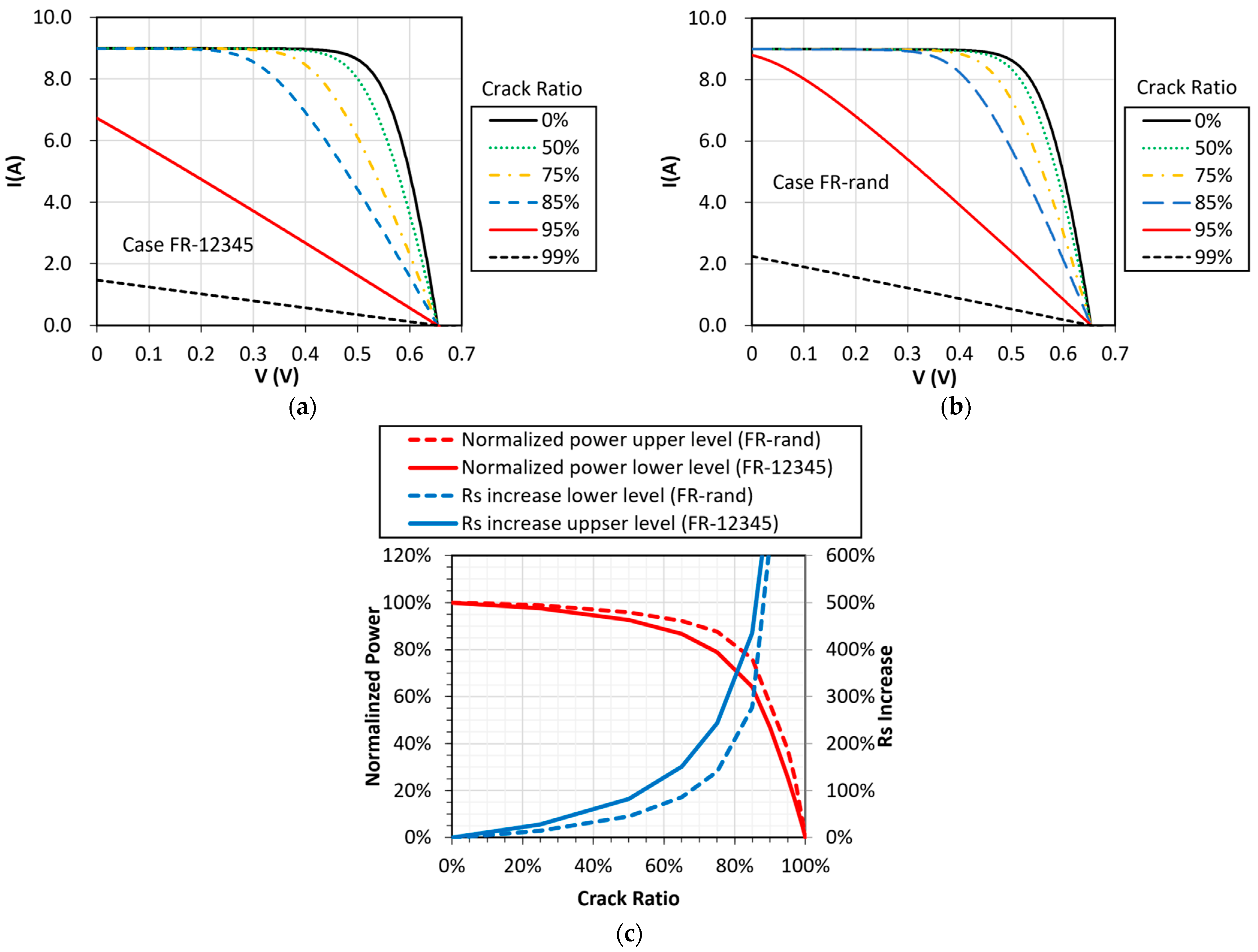
3.3. Power Drop Analysis

To estimate the practical amount of  R s  increase in solar cells, the power drops owing to the  R s  increase were studied. The one-diode equivalent-circuit model in Equation (1) for a one-cell module with  I o  = 1.5 × 10⁻⁸ A,  R sh =  25  Ω I ph =  9 A, and a = 1.25 was constructed using a SPICE simulation software application [30]. The increased  R s  values for the calculation were extracted from Figure 15b.
The calculated I–V curves with several crack ratios for Cases FR-12345 and FR-rand are shown in Figure 21a,b, respectively. From the curves, the maximum powers were calculated, and they are plotted in Figure 21c with respect to the crack ratios for both the cases. It was found that the power is maintained at 71 to 82% when the solar cell had 80% cracked RWs and it drops rapidly after that.
The lifetime of a solar module can be defined as a power drop over 80%, which is a typical choice for many manufacturers’ power warranty time [24]. When the solar cell power decreased to 80%, the  R s  increases are analyzed to be in the range of 200 to 250% for the continuous and random models, respectively.

4. Conclusions

Quantitative analysis was conducted using a 3D FE model to study the effect of solder layer cracking on the  R s  increase in Si solar cells. The model consisted of a Si wafer, front Ag electrodes, back Al electrodes, Cu ribbon wires, and solder layers in a real solar cell with an equivalent resistivity to the absorber layer of the Si wafer. For the  R s  calculation, an electric potential was applied at the end of the busbars, and the amount of current flowing across the solar cell was calculated by summing the current at the end of the busbars.
Two types of cracking models were considered: continuous and random. In the continuous crack model, or when all the RWs on the front side were cracking from bottom to top, it was expected that the current would drop from 0 to 100%, linearly and  R s  would increase exponentially to infinity. However, it was less than 250% until all the RWs were cracked to 75%. Less drops and increases were estimated when cracks were present on the rear side of the RWs. In the random crack model, the current dropped slowly, and the value of  R s  increase reduced compared to the continuous crack model. A simple mathematical model based on the bypass mechanism of the currents was suggested to explain the differences between the models. It was found that cracking in the solder layer under TC is a combination of continuous and random models, and the two models can represent the upper and lower levels of the  R s  increase. When the solar cell power dropped to 80%,  R s  increase was analyzed to be in the range of 200 to 250% using the continuous and random models, respectively.

Funding

This study was supported by the National Research Foundation (NRF; grant number: 2021R1F1A 1052595) and the Korea Evaluation Institute of Industrial Technology (KEIT; contract number: 20017488) of the Republic of Korea.

Data Availability Statement

Data available on request.

Conflicts of Interest

The author declares no conflict of interest.

References

  1. Jordan, D.C.; Silverman, T.J.; Wohlgemuth, J.H.; Kurtz, S.R.; VanSant, K.T. Photovoltaic failure and degradation modes. Prog. Photovolt. Res. Appl. 2017, 25, 318–326. [Google Scholar] [CrossRef]
  2. Skoczek, A.; Sample, T.; Dunlop, E.; Ossenbrink, H. Electrical performance results from physical stress testing of commercial PV modules to the IEC 61215 test sequence. Sol. Energy Mater. Sol. Cells 2008, 92, 1593–1604. [Google Scholar] [CrossRef]
  3. Jeong, J.; Park, N.; Hong, W.; Han, C. Analysis for the degradation mechanism of photovoltaic ribbon wire under thermal cycling. In Proceedings of the 2011 37th IEEE Photovoltaic Specialists Conference, Seattle, WA, USA, 19–24 June 2011. [Google Scholar]
  4. Jeong, J.; Park, N.; Han, C. Field failure mechanism study of solder interconnection for crystalline silicon photovoltaic module. Microelectron. Reliab. 2012, 52, 2326–2330. [Google Scholar] [CrossRef]
  5. Sharma, V.; Chandel, S.S. Performance and degradation analysis for long term reliability of solar photovoltaic systems: A review. Renew. Sustain. Energy Rev. 2013, 27, 753–767. [Google Scholar] [CrossRef]
  6. Kumar, S.; Gupta, R. Thermo-mechanical degradation at finger-solder interface in a crystalline silicon photovoltaic module under thermal fatigue conditions. In Proceedings of the 2019 IEEE 46th Photovoltaic Specialists Conference (PVSC), Chicago, IL, USA, 16–21 June 2019; pp. 0118–0121. [Google Scholar]
  7. Burgelman, M.; Nollet, P.; Degrave, S. Modelling polycrystalline semiconductor solar cells. Thin. Solid Films 2000, 361–362, 527–532. [Google Scholar] [CrossRef]
  8. Malm, U.; Edoff, M. 2D device modelling and finite element simulations for thin-film solar cells. Sol. Energy Mater. Sol. Cells 2009, 93, 1066–1069. [Google Scholar] [CrossRef]
  9. Brown, G.F.; Ager, J.W.; Walukiewicz, W.; Wu, J. Finite element simulations of compositionally graded InGaN solar cells. Sol. Energy Mater. Sol. Cells 2010, 94, 478–483. [Google Scholar] [CrossRef]
  10. Shiradkar, N.; Schneller, E.; Dhere, N.G. Finite element analysis based model to study the electric field distribution and leakage current in PV modules under high voltage bias. In Reliability of Photovoltaic Cells, Modules, Components, and Systems VI; SPIE: Bellingham, WA, USA, 2013; p. 88250G. [Google Scholar]
  11. Asadpour, R.; Sun, X.; Alam, M.A. Electrical Signatures of Corrosion and Solder Bond Failure in c-Si Solar Cells and Modules. IEEE J. Photovolt. 2019, 9, 759–767. [Google Scholar] [CrossRef] [Green Version]
  12. Asadpour, R.; Patel, M.T.; Clark, S.; Bosco, N.; Silverman, T.; Alam, M.A. Worldwide Physics-Based Lifetime Prediction of c-Si Modules Due to Solder-Bond Failure. IEEE J. Photovolt. 2022, 12, 533–539. [Google Scholar] [CrossRef]
  13. Ulaby, F.T.; Michielssen, E.; Ravaioli, U. Fundamentals of Applied Electromagnetics; Pearson: Boston, MA, USA, 2015. [Google Scholar]
  14. Luque, A.; Hegedus, S. Handbook of Photovoltaic Science and Engineering; John Wiley & Sons: Hoboken, NJ, USA, 2011. [Google Scholar]
  15. ANSYS. Chapter 5—Electromagnetics. In Mechanical APDL 2019 R2 Theory Reference; ANSYS: Canonsburg, PA, USA, 2019. [Google Scholar]
  16. ÇadIrlI, E.; Böyük, U.; Kaya, H.; Maraşli, N.; Aksöz, S.; Ocak, Y. Dependence of electrical resistivity on temperature and Sn content in Pb-Sn solders. J. Electron. Mater. 2011, 40, 195–200. [Google Scholar] [CrossRef]
  17. Giancoli, D. Electric currents and resistance. In Physics for Scientists and Engineers with Modern Physics; Pearson Education: New York, NY, USA, 2009; Volume 4. [Google Scholar]
  18. Serway, R.A.; Jewett, J.W. Principles of Physics; Saunders College Pub.: Fort Worth, TX, USA, 1998; Volume 1. [Google Scholar]
  19. López-Escalante, M.C.; Martín, F.; Ramos-Barrado, J. Grouping by bulk resistivity of production-line mono-crystalline silicon wafers and its influence on the manufacturing of solar cells modules. Sol. Energy 2016, 131, 61–70. [Google Scholar] [CrossRef]
  20. Guo, S.; Aberle, A.G.; Peters, M. Investigating local inhomogeneity effects of silicon wafer solar cells by circuit modelling. Energy Procedia 2013, 33, 110–117. [Google Scholar] [CrossRef] [Green Version]
  21. Grote, D. Analyses of Silicon Solar Cells and Their Measurement Methods by Distributed Circuit Simulations and by Experiment. Ph.D. Thesis, Universität Konstanz, Konstanz, Germany, 2010. [Google Scholar]
  22. Schroder, D.K.; Meier, D.L. Solar cell contact resistance—A review. IEEE Trans. Electron Devices 1984, 31, 637–647. [Google Scholar] [CrossRef]
  23. Honsberg, C.B.; Bowden, S.G. Photovoltaics Education Website. 2019. Available online: www.pveducation.org (accessed on 17 January 2023).
  24. Park, S.; Han, C. Reliability-driven design optimization of si solar module under thermal cycling. J. Mech. Sci. Technol. 2022, 36, 4099–4114. [Google Scholar] [CrossRef]
  25. Park, S.; Han, C. Analysis of EL images on Si solar module under thermal cycling. J. Mech. Sci. Technol. 2022, 36, 3429–3436. [Google Scholar] [CrossRef]
  26. Roy, S.; Kumar, S.; Gupta, R. Investigation and analysis of finger breakages in commercial crystalline silicon photovoltaic modules under standard thermal cycling test. Eng. Fail. Anal. 2019, 101, 309–319. [Google Scholar] [CrossRef]
  27. Schmauder, J.; Kurz, K.; Schneider, A. Extended Thermal Cycling Lifetime Testing on Crystalline Silicon Solar Modules with Artificially Introduced Defects. In NREL PV Module Reliability Workshop; NREL: Golden, CO, USA, 2016. [Google Scholar]
  28. IEC 61215-1; Terrestrial Photovoltaic (PV) Modules—Design Qualification and Type Approval—Part 1: Test Requirements. IEC: Geneva, Switzerland, 2016.
  29. Fuyuki, T.; Kondo, H.; Yamazaki, T.; Takahashi, Y.; Uraoka, Y. Photographic surveying of minority carrier diffusion length in polycrystalline silicon solar cells by electroluminescence. Appl. Phys. Lett. 2005, 86, 262108. [Google Scholar] [CrossRef]
  30. Analog Devices. LTspice. Available online: https://www.analog.com/en/design-center/design-tools-and-calculators/ltspice-simulator.html (accessed on 26 December 2022).
Figure 1. Flow chart of the simulation process in this study.
Energies 16 02524 g001
Figure 2. (a) Solar cell one-diode equivalent circuit, (b R s  defined in the I–V curves, and (c) simulation circuit model to estimate  R s .
Energies 16 02524 g002
Figure 3. Electrostatic FE model of the solar cell with ribbon wire: (a) front, (b) rear, and (c) detail view.
Energies 16 02524 g003
Figure 4. Resistance components in a Si solar cell (adapted from [22]).
Energies 16 02524 g004
Figure 5. Schematic of the boundary conditions applied to the model: (a) side and (b) front view.
Energies 16 02524 g005
Figure 6. Contour plots of electric potential on the cell at the: (a) front and (b) rear sides.
Energies 16 02524 g006
Figure 7. Contour plots of current density on the cell at: (a) x-direction (horizontal), (b) y-direction (vertical), and (c) illustration of current flow (based on the results).
Energies 16 02524 g007aEnergies 16 02524 g007b
Figure 8. FE model with cracked solder layer.
Energies 16 02524 g008
Figure 9. Contour plots of: (a) electric potential and (b) current density on the cell in the x-direction for the solar cell with cracked solder layer.
Energies 16 02524 g009
Figure 10. Change in current at the front RWs when there is a cracked solder layer at the front RW3.
Energies 16 02524 g010
Figure 11. Simulation results for Cases F-1 and F-3: (a) current drop and (b R s  increase over crack ratio.
Energies 16 02524 g011
Figure 12. Simulation results for Case F: (a) current drop and (b R s  increase over crack ratio.
Energies 16 02524 g012
Figure 13. Simulation results for Case R: (a) current drop and (b R s  increase over crack ratio.
Energies 16 02524 g013
Figure 14. Comparison of simulation results for Cases F, R, and FR: (a) current drop and (b R s  increase over crack ratio.
Energies 16 02524 g014
Figure 15. Comparison of simulation results for Cases FR-12345 and FR-rand: (a) current drop and (b R s  increase over crack ratio.
Energies 16 02524 g015
Figure 16. Index definition in the crack and current density model of Equations (15) and (16).
Energies 16 02524 g016
Figure 17. Graphical representation of: (a Crack ( m , k )  and (b CurrentDensity ( n , k )  functions for Cases FR-12345 and FR-rand with 50% crack ratio for a solar cell.
Energies 16 02524 g017
Figure 18. Current drop calculation results from Equation (16) for Cases FR-12345 and FR-RD.
Energies 16 02524 g018
Figure 19. Contour plot of current density of Si wafer for: (a) Case FR-12345 and (b) Case FR-rand with 50% crack ratio.
Energies 16 02524 g019
Figure 20. Example EL image of a solar module after 1000 TC.
Energies 16 02524 g020
Figure 21. Circuit simulation results: (a) I–V curves for Case FR-12345, (b) I–V curves for Case FR-rand, and (c) power drop and  R s  increase plot over crack ratio.
Energies 16 02524 g021
Table 1. Selected resistivity of the materials in the model for electrostatic analysis.
MaterialsResistivitiesReferences
Solder (Pb40Sn60)1.50 × 10⁻⁴ Ω-mm[16]
Copper1.68 × 10−5 Ω-mm[17]
Silver1.59 × 10−5 Ω-mm[18]
Aluminum2.65 × 10−5 Ω-mm[18]
Si wafer   Bulk   resistivity   ( ρ b ) 30 Ω-mm[19]
  Emitter   sheet   resistance   ( R E S ) 55 Ω/sq.[20,21]
  Contact   resistance   ( ρ c ) 0.3 Ω-mm2[20,21]
Table 2. Definition of simulation cases.
NotationDescription *
Case 0No cracking
Case FCracking in the RWs at front side:
Case F-1continuously from bottom to top at RW1.
Case F-3continuously from bottom to top at RW3.
Case F-123continuously from bottom to top at RWs 1, 2, and 3.
Case F-12345continuously from bottom to top at RWs 1, 2, 3, 4, and 5.
Case RCracking in the RWs at rear side:
Case R-1continuously from bottom to top at RW1.
Case R-3continuously from bottom to top at RW3.
Case R-123continuously from bottom to top at RWs 1, 2, and 3.
Case R-12345continuously from bottom to top at RWs 1, 2, 3, 4, and 5.
Case FRCrack in the RWs at both front and rear sides:
Case FR-12345continuously from bottom to top at RWs 1, 2, 3, 4, and 5.
Case FR-randin random at RWs 1, 2, 3, 4, and 5.
* RW numbered 1–5 from left to right.
Disclaimer/Publisher’s Note: The statements, opinions and data contained in all publications are solely those of the individual author(s) and contributor(s) and not of MDPI and/or the editor(s). MDPI and/or the editor(s) disclaim responsibility for any injury to people or property resulting from any ideas, methods, instructions or products referred to in the content.

