Abstract
The main drawback of DC-source-based renewable energy sources (RESs), such as photovoltaic (PV) panels or fuel cells (FCs), is that the voltage generated by a panel or cell is less than the required voltage for connection to a DC–AC inverter for grid applications. In this paper, a single-switched DC–DC boost converter equipped with a quasi-impedance source inverter (QZSI) with a modified switching model is proposed to increase the output voltage of these RESs and convert it to a fixed AC grid voltage for loads. By changing the position of the inductor in a classic step-up converter and using a switched-inductor block, the input current ripple is significantly decreased, and the reliability and long-life of the input sources are increased, which is the main contribution of this work. The quality of the generated AC voltage and the low amount of total harmonic distortion (THD) in the projected topology are significant, and no overshoot and undershoot have been reported for both output voltages and currents under different operating conditions with variable loads. Theoretical analysis, simulation results, and comparison with similar topologies are examined and a prototype with a power of 200 to 400 watts is presented. Experimental results confirm the theoretical studies.
1. Introduction
By considering the increasing need for electricity, researchers are looking to generate electricity in different ways using existing energy sources. Given the limited sources of fossil fuels and the dangers and limitations of nuclear fuels, the interest in using renewable energy sources (RESs) is growing day by day.
Solar cells, batteries, and hydrogen energy-based fuel cells are devices that use different types of energy and convert these energies directly into electrical current or voltage. Today, these RESs are used in various applications, such as battery charging, electric vehicles (EVs), electric charging stations, water pumping, home and grid power supply applications, and off-grid and satellite energy systems [1,2]. In order to use these sources, a series of intermediate equipment and electronics converters are needed to prepare acceptable electrical energy to the electrical loads. One of the most important components of this equipment is power electronic converters that are used to increase or decrease the input voltage level, enhance the power quality control, reduce the harmonics, and convert DC to AC voltage or vice versa in these systems [3,4,5]. DC–DC and DC–AC converters are among the most widely used power converters in this field. Some environmental factors can change the voltages and currents produced by these DC sources. For example, temperature, radiation, a combination of electrolyte and chemical components, and contamination and proportions of oxygen and hydrogen particles can instantly change voltages and currents [6,7,8].
Generally, the generated voltage of these sources is limited, and these low-voltage RESs are equipped with DC–DC converters before connecting to the power grid. The gain of DC–DC boost converters is theoretically infinite when the duty cycle is equal to one, but in practice, as the duty cycle increases, the voltage gain and efficiency of the converter decrease sharply. The reason for this is that through longer duty ratios, the dynamic losses due to the high number of current peaks in the components increase, and the voltage stress across the switch and diode which is equal to the output voltage of the converter in a conventional boost converter increases. Since an internal resistor is modeled for the switch and diode, larger currents lead to more power losses across these resistors with larger voltage drop values.
To solve these problems, various types of DC–DC converters have been proposed [9,10,11,12,13]. Basically, these converters offer techniques, such as voltage multiplier cells, coupled-inductor blocks, fly-back converters with transformer blocks, and a combination of these methods, to obtain higher voltage gain values. One of the disadvantages of these converters is the hard switching operating mode, which reduces the efficiency of the converter. In addition, their bulky and heavy components directly increase the volume and price of the circuit. In addition, the current ripple in these converters is usually high, which reduces the lifespan of the RES connected to these circuits. In these converters, a large filter must be used on the input side to eliminate the input current ripple.
On the other hand, in single-phase operations, the power density and efficiency of the converter are reduced. To improve the efficiency of the converter in the high-power ranges, researchers have proposed two-phase and three-phase interleaved methods in which the power is divided between the phases and the input current ripple is reduced, resulting in reduced losses and higher efficiency. Concerns and drawbacks about these structures are the high numbers of components used in the converter topology, which cause problems, such as bulky and heavy structures with expensive topologies and complexity in control processes [14,15]. In this study, different boost topologies were considered and their features, advantages, and disadvantages were investigated [16,17,18,19,20].
After obtaining an appropriate level of DC voltage, a DC–AC inverter block is applied to generate a sinusoidal voltage waveform at the grid voltage level for loads. Half-bridge (HBI) [21], full-bridge (FBI) [22], voltage source (VSI) [23], current source (CSI) [24], H5 [25], H6 [26], and HERIC [27] inverters are among the most used and considered topologies. Grid connection conditions and the necessity to apply a filter to the output side of the inverters, which requires precise and sometimes complex controller and switching topologies; high THD values for the output current and voltage; and the low-gain range of these inverters are the main drawbacks of these converters.
Meanwhile, impedance source inverters (ZSIs) are relatively efficient converters, and the application of these inverters is increasing day by day [28,29,30]. These inverters in the simplest design consist of two capacitors and two inductors. Conventional ZSI consists of an X-shaped impedance network. The shoot through (ST) feature is used to enhance the voltage in these converters.
Different topologies for these types of inverters have been presented by researchers for better performance and higher efficiency and reliability.
ZSI converters can also be used as step-up converters [31,32] or as a half-bridge-ZSI [33]. Different indicators are considered to evaluate these converters according to their type and application under different duty ratios, such as the number of components, voltage and current stresses across the semiconductor devices and inductors, the ripple of the input current, and the ripple for the output voltage. In this regard, one of the most important features of ZSIs is the voltage gain, which has led to the provision of different structures for these converters. Various structures for the quasi-ZSI (Q-ZSI) have been proposed in the studies. For example, the series-ZSI (SZSI) is proposed to decrease the voltage stress across the capacitors [34,35]. Despite the low voltage value of the capacitors in SZSI, the main part of the current of the impedance network flows through these capacitors which directly enhances their nominal capacitance value. These structures have fewer passive components than a conventional ZSI and often have the advantages of ZSI, but their voltage gain is still low. For obtaining more voltage gain for the ZSI, a new converter was proposed in reference [36] for switching boost inverters.
In some other studies, in order to achieve higher voltage gains, improved structures, such as cascaded converters or topologies with transformers, are presented. In reference [36], the impedance source inverter with a switched-inductor cell (LZSI) is presented, which increases the voltage by removing the capacitors of the ZSI using the switched-inductor cell. A quasi-ZSI is presented in [37] in which the voltage gain is increased by the addition of the capacitor and inductor blocks. Ref. [38] provides an impedance source inverter equipped with a switched capacitor configuration and a bridge inverter with an output filter. In [39], the transformer circuit was removed, and an inductor network with a bridge inverter cell was used. In [40], a ZSI block based on the quadratic converter is presented. The advantage of the proposed topology is no need for high voltage gains, and the quality of the generated power is good. However, every Z-network should be equipped with a full bridge inverter which causes lower efficiency for this topology. Due to the fact that in RESs the generated voltage is usually in the low range, this shortage should be compensated in some way. For example, in solar systems, it is necessary to generate electricity in a wide range of voltages by using a large number of modules in series, which increases the cost of electricity production. Some of the details regarding electromagnetic interference calculations are presented in [41]. Different inverter topologies and switching and control methods are analyzed in [42,43,44,45,46,47,48,49,50].
To solve these problems, in this paper, a novel switched-inductor-based single-switch DC–DC boost converter is presented, and then a QZS inverter converts the DC output voltage of the boost converter to AC through an improved sinusoidal pulse width modulation (SPWM) technique. Different levels of the input voltage source are examined, and the stability of the boost converter for generating a fixed voltage at the input side of the QZSI block is tested. A wide range of resistive and resistive-inductive loads are connected to the QZSI output nodes, and the quality of the proposed switching model is presented. The low-ripple current waveform at the input side of the converter and pure sinusoidal voltage at the output side are among the advantages of the proposed topology and controllers. In addition, the value of the THD is very low, and the reaction of the converter by changing the loads is significant, where no overshoot or undershoot has been reported at the load changing time for the voltage and current waveforms. Mathematical investigations are presented, and finally, a 200 to 400 W prototype converter confirms the correctness of the theoretical analysis.
The proposed converter can be used in micro-grid applications and locations where the electricity grid cannot be reached and the energy of the location is generated by renewable energy sources (RESs), such as PV panels, off-grid home and green energy applications, or converting the energy of electric vehicles (EVs) to the requested AC voltages in off-grid locations through vehicle-to-grid (V2G) charging stations. Uninterruptible power supplies (UPSs) and DC power source usages are other possible applications of the proposed converter.
2. The Proposed Configuration and Switching Method
Figure 1 presents the general DC voltage-based configuration with DC–DC converter block and inverter structure. Since the generated voltages of conventional DC sources are not enough to be connected directly to the DC–AC inverter, a DC–DC boost converter is normally applied. Meanwhile, the output of the boost converter also needs to stay at the constant level of the voltage by changing the input voltage of the converter and also the different amounts of the loads at the output side of the converter. Therefore, a feedback mechanism is applied to measure the output voltage, compare it with the desired output DC voltage, and change the duty ratio of the power switch if an error signal is formed. Then, the inverter block is activated to change the DC voltage to the AC in order to supply the necessary voltage and current for the grid or AC load. The general configuration for integration of the DC sources with the grid is shown in Figure 1.
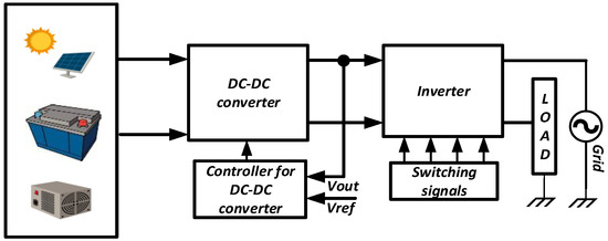
Figure 1.
General configuration of the PV-based inverters for AC loads or grid applications.
Figure 2 shows the proposed converter. As can be seen, both the DC–DC boost converter and the proposed ZSI and the full-bridge-based inverter are presented by the DC–DC converter and inverter boxes, respectively. The details for these topologies will be presented in Section 2 and Section 3. The internal topology of the DC–DC step-up converter is formed by using the conventional boost converter by replacing the location of the elements innovatively and by using a switched-inductor cell instead of the conventional inductor. To analyze the projected step-up converter, Figure 3 presents and investigates the state of the semiconductor devices and charging or discharging states of the inductors and capacitors in two different operational modes. These states can be seen in Figure 3a,b. These figures present the topology of the converter for time durations that the power switch is in on and off modes, respectively.
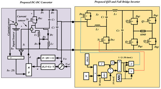
Figure 2.
The proposed converter and its controller.
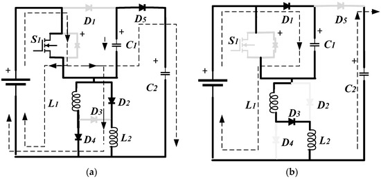
Figure 3.
The proposed DC–DC boost converter for the time durations that the switch is in (a) on and (b) off-states.
The proposed inverter circuit is formed by the QZS inverter with integration with the full-bridge inverter (FBI). The proposed QZSI circuit is formed by using two power switches, two inductors, and two capacitors. The reaction of the elements on this side is complementary, and MOSFET transistors can simply be switched. This converter prepares a full-waved sinusoidal voltage and current waves for the FBI block, and finally, the FBI converts these waveforms to the sinusoidal voltage and current signals. The inverter section, separately, will be investigated in Section 2.4.
2.1. The Gain of the Proposed Boost Converter
The proposed DC–DC converter can be seen in Figure 2 with the light purple color. Switched-inductor cells prepare DC–DC converter circuits to operate at higher power ratings. The main reason for this is that in the on-state of the switch in the circuit, the inductors become parallel and can pull a higher current from the input power supply. When the switch is opened, the inductors become in series. In this way, they can transfer higher values of the power to the load. However, since they are discharged in series, a more ripple-free state of the current drawn from the input source can be achieved since a larger inductor value is obtained. This state prepares the converter for high-power and low-ripple applications. However, for a conventional boost converter, no possibility exists for charging in parallel and discharging in series for inductors. Furthermore, the second end of an inductor in a classical boost converter is connected to the switch and diode, and the current is changed by the on- and off-states of these semiconductor devices. However, by changing the location of the switch with the inductor, since the input source is connected to the inductor via the switch, the discharging process of the inductors will be slower. For obtaining the gain of the proposed DC–DC boost converter, the state of the converter should be analyzed separately for the time duration the power MOSFET is in on and off modes, respectively. Below, these two different modes are presented:
State 1: The configuration of the proposed topology for this operational mode is illustrated in Figure 3a. As can be seen, in this state the switch is activated. Both inductors L1 and L2 will be parallel with the input voltage source and start to be charged through the power diodes D2 and D4. Diode D3 is reversed biased and could not activate. The negative pole of capacitor C1 is connected to the positive pole of the input voltage, and this forces the capacitor to discharge across capacitor C2 through diode D5. The capacitor C2 is responsible for the ZSI input voltage side and will be ready to energize this block.
For a simple mathematical analysis, the power components are considered to work ideally, and the internal resistance of the switch and diodes are ignored. Therefore, the voltage across inductors L1 and L2 can be shown by:
In this equation, indicates the input voltage source. For the symmetrical conditions of the inductors, it is considered that inductors L1 and L2 are the same and can be represented by L.
State 2: The configuration of the proposed converter can be seen in Figure 3b for this working mode. Since the switch is in the off-state, diode D1 starts to handle the input current and charge capacitor C1. By charging this capacitor, both inductors begin to be discharged, and a serial connection is formed between them. Since this topology presents a voltage greater than the input voltage, diode D5 is deactivated, and the voltage across capacitor C2 starts to discharge across the ZSI block.
For this state, one can simply write:
Therefore, the voltage across the inductors can be calculated by (3):
Since for a time period the average voltage value across an inductor is zero for a switching circuit, Equation (4) can be written:
where D and (1 − D) indicate the ON and OFF-states of the power switch. In fact, D is the duty ratio of the switch and indicates the time duration that the switch is activated in a time period. The voltage across capacitor C1 can be written:
Since the average voltage across the inductor is zero, the voltage across capacitor C2 can be calculated the same as capacitor C1, and the DC gain of the boost converter can be found as:
2.2. Inductors and the Current Ripples
Input current ripple is one of the most important features for a DC–DC converter, and topologies with the least ripple values are preferred. The reliability of the converter and the long life of the components in the circuit, especially power semiconductors, are the reason for the minimum ripple for the input current. When the input source is a PV array, this feature will be more important since the large variations for the current directly decrease the useful long life of the module. In order to find the current ripple, the magnitude of the currents for two on- and off-states of the switch should be considered. For the time duration that the switch is in the on-state, the current for the inductors can be calculated through (7) and (8). In addition, for the next time duration that the switch is in the off-mode, the current magnitude can be presented by Equations (9) and (10).
where and , respectively, present the current magnitude for the inductors for the time durations that the power switch is in the on- and off-states. Since the is the same with , they can be replaced in equations. Since for the steady-state operation, the change of the current should be zero for the inductor, from (8) and (10) one can write:
By considering the and as the input and output powers for the converter and as the load:
This equation can present the average current value for the inductor current:
Since this current is the average value for the inductor current, the pick currents (minimum and maximum amplitudes) can be presented by:
Continuous conduction mode (CCM) indicates that the current of the inductor is always positive. Therefore, the minimum current of the inductor should be greater than zero. This current can be shown by . When , the inductor value has been selected for the boundary condition (BCM) between CCM and discontinuous conduction mode (DCM). It means for the CCM operational mode; the value of the inductor should be selected at least 25 percent greater than the calculated value for BCM.
where indicates the switching frequency. From (17), a relation between and can be obtained:
2.3. Capacitor and the Voltage Ripples
Another important feature for a proper power converter circuit is its ability to present a fixed voltage at the load side and across the output voltage. It is preferred to have a maximum 1 percent ripple for this voltage. To obtain this voltage ripple value, Equation (19) can be used:
In this equation, presents the electrical charge of the capacitor for the time duration that the capacitor is charged. Voltage fluctuation can be calculated simply:
The recent equation shows that the value of this capacitor is directly in a relationship with the voltage fluctuation magnitude:
Figure 4 shows the switching voltage for the power switch, voltage across the diodes, current for the capacitors, and voltage and current for the inductors to present the state of the components in a switching time period.
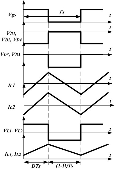
Figure 4.
Switching voltage for the power switch, voltage across the diodes, current for the capacitors, and voltage and current for the inductors in a switching time period.
2.4. Controller Design
For the proposed converter, when the switch is in the on-state, Equation (23) can be written:
presents the amount of the output load and can be considered as the input impedance for the next block, ZSI. Here, , ,and present the input current of the converter, the current of the inductors, and the output signal for the controller as can be found for a PI controller in the literature.
By using the Laplace transform, we can obtain:
Therefore, the duty cycle can be related with the , , and :
To obtain the control signal, Figure 5 is presented and simply shows the relation between these parameters. Since the classic PI or PID controller is considered to be designed, the general transfer function of the PID controller, , is written, and the coefficients can be calculated:
Figure 5.
The proposed DC–DC converter circuit and controller.
The closed-loop form of the controller can then be written as:
The and coefficients can be calculated as below:
2.5. Operation of the Quasi Z-Source Inverter
Figure 6 illustrates the state of the QZSI when the switches S2 and S3 are activated and deactivated. The working principle of this converter makes the power switches activate complementarily, and in the per time interval, only one of the switches will be in the on-mode. This is a useful feature of this converter since it simplifies the switching and controller structure design. In addition, a unilateral sine wave can be generated at the output side of this inverter that can improve the THD of the converter without the need for the filter designs.
Figure 6.
The state of the QZSI when the power switch (a) S2 or (b) S3 is activated.
A comprehensive explanation of the operating conditions of this converter is presented in [2]. This converter can be used in both CCM and DCM with different values of the duty ratios , and modulation indexes .
The state of the voltages and currents of the various components in this converter is depicted in Figure 7. As can be seen, for the time intervals that S2 is activated, S3 is deactivated and vice versa. When S2 is in the on-mode, inductor L3 is charged through this switch, and inductor L4 is discharged by capacitors C4 and C3. For the next time interval, S3 is activated, the voltage across capacitor C3 is discharged, and the current of inductor L3 begins to decrease. Meanwhile, the input voltage starts to charge inductor L2 and capacitor C4. These details can be followed in Figure 6a,b. In addition, the state of the voltage and currents for components of the QZSI block are shown in Figure 7. As can be seen in Figure 7, two opposed switching signals are considered to apply to the switches in the QZSI block. On this occasion, inductors L3 and L4 with be charged and discharged asynchronously and oppositely. The presence of positive voltage at both ends of an inductor ensures that the current through the inductor rises and charges. Conversely, at negative voltages, the current of the inductor starts to decrease, and the discharge process takes place. All these facts can be followed through Figure 7.
Figure 7.
The state of the voltage and currents for the components of the QZSI block.
For the steady-state operational conditions, by considering the as the duty cycle of the power switch S2, the gain of the QZS inverter , is obtained by (29):
In addition, for this converter, the output voltage can be presented by (30):
By considering the as the maximum magnitude of the generated voltage across capacitor C4, the modulation index can be calculated by:
where indicates the input voltage for the QZSI block. By considering Equations (29)–(31), the duty ratio, for the power switch S2 can be obtained as:
Since the duty ratio, for the switch S3 is equal to , one can simply obtain:
Equations (32) and (33) show that for higher modulation indexes, the negative values for the duty ratios will be obtained; therefore, these equations can be rewritten for obtaining an AC voltage with peak values equal to the input DC voltage:
In practice, achieving this seems to be easier for preventing the complexity of the controller. The results of the switching of the switches can be seen in Figure 8. The obtained voltage across capacitors C3 and C4 shows that a full-wave rectified voltage will appear across capacitors C3 and C4, and it will be suitable to convert to a sinusoidal voltage across the load by applying a full-bridge inverter (FBI) as can be seen in Figure 8.
Figure 8.
Voltage states across the capacitors of the QZSI and drain-source pins of the FBI switches.
Voltage across capacitors C3 and C4 can be obtained by:
Therefore, the voltage ripple across these capacitors can be presented by:
In addition, the current ripple for the inductors can be calculated by (37):
The improved switching model for the proposed QZSI can be presented by Figure 9 according to Equation (34).
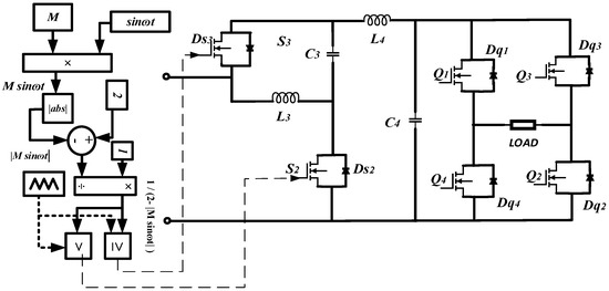
Figure 9.
The proposed sinusoidal PWM model for the QZS inverter.
Figure 10 presents a conventional full-bridge inverter (FBI) that can easily convert the input voltage to a sinusoidal voltage. Since the voltage of capacitors C3 and C4 is connected to this block, as can be seen in Figure 8, a pure sine wave for voltage is obtained. The state of the FBI switches can be seen in Figure 10a,b. These power MOSFETs are switched simultaneously by a square wave-pulse with 50 Hz frequency suitable for grid applications. Switches Q1 and Q2 will be activated under conditions that switches Q3 and Q4 are deactivated and vice versa.
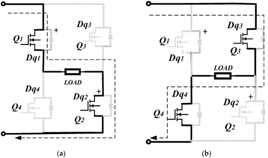
Figure 10.
Full bridge inverter block and the state of the MOSFFETs when (a) Q1 and Q2 and (b) Q3 and Q4 are switched.
2.6. Losses Calculations for the Proposed Converter
The power losses for the DC–DC step-up converter circuit can be divided into dynamic and switching losses. Dynamic losses are in direct relation to the internal resistance of the inductors, capacitors, and semiconductor devices when the current is established. Switching losses can be calculated for power switches and diodes and will occur at the switching times when the voltage and current of the device form a cross point and generate a power loss under the real working conditions. Theoretically and in ideal operational modes, when a switch or diode is connected, the voltage across the device will sharply decrease and reach zero, but in practice the voltage of the mentioned element needs time to be zero. To overcome the switching losses, soft switching techniques including the zero voltage (ZVS) and zero current switching (ZCS) techniques should be considered. Basically, in these techniques, a small and serial inductor is applied with the semiconductor devices, and a parallel capacitor is used across them.
Inductors:
Generally, two core and dynamic losses are considered for the inductors. The core losses normally are presented by the supplier and can be calculated through Equation (38):
In this equation, , , and present a constant for the core material, switching frequency, and flux density, respectively. In addition, , and represent the flux density exponent and effective core volume. This type of loss is small and is discussed in mill-watts.
Dynamic or conduction loss for an inductor can be calculated through Equation (39):
DC resistance of the inductor is indicated by , and presents the root mean square (RMS) value of the current. With an appropriate approximation, can be considered as the average current of the inductor. The total dissipated conduction losses for the inductors can be found by.
Capacitors:
The general state of the loss equation can be written by:
Simply, and indicate the equivalent serial resistance and RMS current of the capacitor. Since is very small, normally the loss of the capacitor is ignorable. The total power loss for capacitors is equal to:
Mosfets:
The conduction power dissipated in a power MOSFET can be formulated by:
As mentioned for the inductors, represents the internal resistance of the switch when it is activated, and is the RMS current for the switch. Since the switching losses also should be considered for the switches, the energy definition during the switching phase and blocking phase should also be considered. This loss value can be found by:
where indicates the switching frequency. Generally, the power loss for a switch is equal to:
Therefore, the total power losses can be formulated by:
Diodes:
Power diodes like the switches have both conduction and switching losses. The conduction loss can be presented by:
where and are the DC resistance of the anode to cathode when the diode is in the on-state and average current of the diode, respectively.
The similar switching losses for diodes can be reported by:
Therefore, the total power loss for a diode is equal to:
Total losses of the diodes can be written by:
The total losses of the converter include the loss for the inductors, capacitors, switches, and diodes:
The efficiency of the converter is:
where is the output power that is transferred by the converter to the load.
2.7. Shoot-Through and Non-Shoot-Through State Working Modes
Figure 11 illustrates the state of the converter when all of the switches are connected and disconnected at the same time. These two working modes are known as the shoot-through (ST) and non-shoot-through (NST)working states and are shown in Figure 11a,b, respectively.
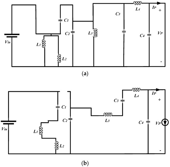
Figure 11.
Equivalent circuits of the proposed inverter: (a) shoot-through state; (b) non-shoot-through state.
To analysis the converter in ST, since a positive charging current is established from the input voltage source to the ground, diode D3 is disconnected. In addition, since the voltage at the output in a boost converter is greater than the input voltage source, diode D1 is disconnected. In these working modes, inductors L1, L2 and capacitor C2 are charged, and C1 is discharged. So, one can simply write:
In addition, since both switches S2 and S3 are connected, all the inductors and capacitors in the ZSI cell will be charged. This state can be followed by Figure 11a.
For the NST working mode (Figure 11b), diodes D1 and D3 are connected, D5 is disconnected, and a serial LCLC network is forming for the ZSI converter elements. For this mode, one can write:
In recent equations, VP and IP are the short circuit and open circuit voltage and current for the output nodes of the inverter.
3. Comparison and Discussion
In this section, the different features of the proposed topology will be compared with some of the conventional and new structures that have been presented in recent years. For this purpose, the converter in two different sections will be discussed. Firstly, the proposed boost converter and then the inverter topologies will be considered. Table 1 presents different boost converters. Table 1 and Figure 12 compare the features of the similar boost converter circuits and the proposed converter. For a better analysis, Figure 12a–c are presented according to the equations in Table 1. For these figures, the duty cycles more than 0.5 are considered that normally are used in designing. In Figure 12a, the gain of the converters is compared. As can be seen, the gain of the proposed converter is considerably high, especially when one compares the number of the components of the converters. The boost converters proposed in reference [17,20], and [18] use 14, 13, and 12 elements, respectively, and converters in [16,18,19] use 11 components, respectively, where the proposed converter and circuit in [51] use only 10 components. The converter in [52] has nine components. The number of the power switches is important since the high numbers of switches need more complex control circuits and strategies. The proposed converter has only one power switch, less than all other converters, [20], and the proposed converter has five diodes. The number of diodes for circuits in [16,17,18] is equal to four. In addition, since the inductor is one of the main sources of power losses based on the internal resistance, this parameter should be considered. The number of inductors is equal to the inductor numbers in [16,18,19] and less than the inductor numbers of the converters [17] and [51]. The gain of the proposed boost converter is comparable with most of these converters. The same results can be reported for the voltage stress across the output capacitor. These results can be followed through Figure 12b. Some of the references in Table 1 enhance the voltage by applying more than one block and one inductor.

Table 1.
Comparison between the proposed and other boost converters.
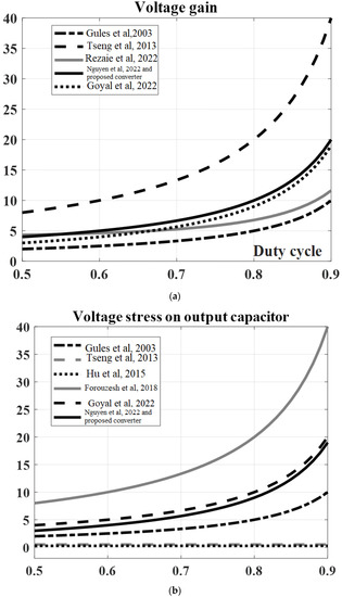
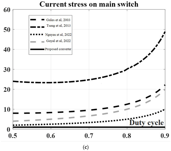
Figure 12.
(a) Voltage gain: (b) voltage and (c) current stresses of the proposed boost converter in comparison with converters in [16,17,18,19,20] and [51,52].
Therefore, for obtaining a result to present, the number of blocks is considered as n = 1 for all of these converters.
One of the main features of a converter is the current stress at the input inductors. This not only reduces the dynamic losses of the converter but also enhances the reliability and long life of the converter. Figure 12c shows this parameter. This figure illustrates that the current stress of the inductors is the least for the proposed converter. The topology of the inductors, especially when making a parallel configuration, is an effective parameter for achieving this specification that can be considered as one of the most important features of the proposed boost converter.
The same comparison is conducted for the proposed inverter block. A number of the new or well-known inverters are presented in Table 2, and Figure 13 analyses the features of the converters. Table 2 shows that the inverters in [36,37,39] have 13 elements, the inverter in [38] has 9, and the proposed inverter in [40] includes 11 components. The proposed converter has only six components in the QZS block and four power switches for FBI topology. Moreover, there is no power diode in the proposed inverter topology. The number of inductors in the proposed converter is less than the inductors in topologies [36,37,39], and the same is true for inverters in [40]. The inverter in [37] has the most, [39] has the least number of capacitors, and the proposed converter and the inverter presented in [36] include only two capacitors.
Table 2.
Comparison between the selected and other Z-source converters.
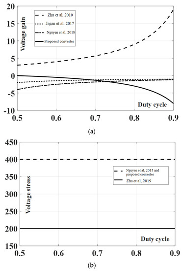
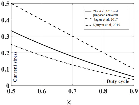
Figure 13.
(a) Voltage gain: (b) voltage and (c) current stresses of the proposed QZSI in comparison with inverters in [16,17,18,19,20] and [51,52].
Figure 13a presents the gain of the inverter circuit in [36] as the most. After that, the proposed converter presents the next highest voltage gain. It is important to consider that a larger duty ratio for charging the inductors and the presence of current in the semiconductor elements that are the main sources of the dynamic losses generates currents with higher amplitudes and ripples that directly increase the power losses across the inductors, switches, and diodes. Therefore, longer duty cycles are not preferred, especially for high-power applications. The state of the gain curves for the inverters shows that the performance of the proposed QZS inverter circuit is appropriate in comparison with the other topologies by considering the number of elements and the ease of control and switching. Figure 13b shows the voltage stress across both power switches in the proposed topology and in comparison with other inverters. Half of the output voltage drops across switch S2, and the other half drops across switch S3. Totally, the output voltage is divided and drops across the switches that, with consideration of the other topologies, present an appropriate result.
The current stresses at the input side of the converters are presented in Figure 13c. This figure shows that the converter in [39] has the minimum current stresses for the input inductor, and this stress is a bit more for the proposed inverter and topology in [36]. Inverters in [37,38,40] have the most value of current stresses. All of these inverter circuits have important topologies and are the basis of new studies according to their advantages. By considering the features of these inverters, the number of used components, and the complexity of the control circuit and algorithm, the proposed inverter topology is comparable and presents many of the advantages.
The voltage and current stresses for the elements of the DC–DC boost converter are presented in Figure 14. Figure 14a,b show the current stresses for the switched-inductor block components including inductors L1 and L2 and diodes D2, D3, and D4. As presented theoretically, the current ripples of the inductors are the same, and the current ripples for the diodes are also equal. These figures show that the ripples of the current passing through the inductors are always smaller than the input. In addition the current ripples of the diodes when activated are always smaller than the input and inductor current ripples. The ripples magnitude for these diodes are considerable in comparison with the inductor current ripples.
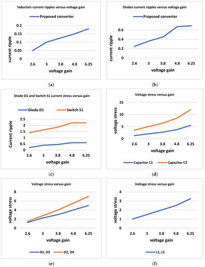
Figure 14.
(a) versus gain; (b) versus gain; (c) versus gain; (d) versus gain; (e) voltage gain; (f) according to gain of the converter.
Figure 14c is one of the most important figures that presents the current stresses of the switch and input diode D1 in comparison with the input current ripple. For all gain values, the current ripples for the main switch are more than the input ripples, and for higher DC gains, this value is increasing. In addition, the state of the ripples for diode D1 shows that the smaller gains cause this diode to pass currents with less ripples, and for higher DC gains, these ripples will increase.
As can be followed through the theoretical analysis and the configuration of the DC–DC converter, the voltage across capacitor C2 is the input voltage for the inverter side, and the stress for this capacitor is the same with output voltage. In addition, the voltage of capacitor C1 is smaller rather than the output voltage and follows the VC2. These states can be seen in Figure 14d.
The reversed biasing voltage across diodes D1 and D5 is reported in Figure 14e. As can be seen, the voltage stress for both of these diodes is the same, and with increasing the gain of the converter, the related reversed voltage also increases.
Finally, the voltage stress for the switch of the DC–DC converter in the proposed converter topology is illustrated in Figure 14f. This figure shows that the voltage stress across the switch is greater with higher DC gains in comparison with the input voltage, but the total voltage stress for the switch is acceptable by considering the amount of the output voltage.
For the ZSI cell, for the voltage equal to 96 VDC as the input voltage, a peak-to-peak voltage equal to 120 V drops across the inductors, and the same voltages are measured across capacitors C3 and C4. The maximum voltage across switches S2 and S3 is equal to the input voltage, and the same input current is reported for the switches. The currents following through the inductors are the same as the input current.
4. Simulation Results
This section presents the simulation results for the proposed converter. Firstly, the main voltage and current signals of the proposed boost converter are presented, and then the results for the QSZI and FBI parts are illustrated. These results are presented for a prototype with 200 to 400 W and is in preparation for the comparison with the results of the laboratory-scaled prototype circuit. To investigate fair theoretical and laboratory experimental studies and comparison, the same value of the elements are used. The component values based on the presented equations are reported in Table 3.
Table 3.
Components values.
Figure 15a presents the input source current, and Figure 15b,c show the switch and diode D1 currents, respectively. This figure indicates that the switch and diode D1 are working oppositely, and when one of these components is activated, the other one will be disconnected.
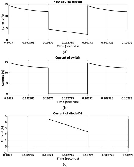
Figure 15.
(a) Input source current and the current of the (b) switch and (c) diode D1 in the proposed boost converter.
In comparison with a conventional boost converter, the current wave at the input side changes at the switching times that causing electromagnetic interferences (EMIs). EMI is an undesired working state and appears in switching converters. EMI should be removed by using a CLC filter and is divided into conducted and radiated EMI. Figure 16 presents the general scheme of the EMI filter that should be located between the input source and the DC–DC converter. is normally selected to be between 1 to 10 µH, most frequently close to 10 µH to support high current applications [41].
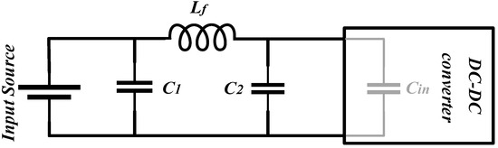
Figure 16.
EMI filter design for the proposed boost converter.
The amount of capacitor C1 is defined by these two equations:
The value of C1 is selected as the higher value of and . In these equations, is the input capacitor of the boost converter, and indicates the switching frequency of the converter. is the requested debilitation according to the decibels and can be found through (57):
where is the peak-to-peak input voltage ripple, and represents the target maximum voltage in decibels. The amount of capacitor C2 is selected between 100 and 150 µF normally and is part of the input capacitors.
Figure 17a,b present the current and voltage waveforms of switch . These figures show that for the time intervals that the switch is activated, a voltage equal to zero drops across the drain-source pins, and for the time durations that the switch is deactivated, the current reaches zero amperes, and the voltage close to the voltage of capacitors and drops across the drain-source pins of this switch. An average current close to 2A is established in drain-source pins of the switch in a switching time period.
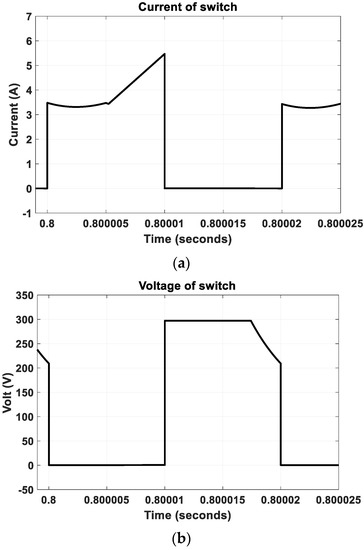
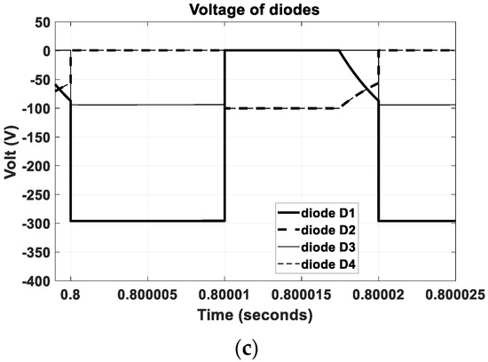
Figure 17.
(a) Current and (b) voltage stresses of switch S1; (c) voltage waveforms across diodes in the proposed boost converter.
Figure 17c shows the voltages across the power diodes in the boost converter. This figure confirms the results that were theoretically presented and shows that diodes are activated at the same time intervals. In addition, the state of diodes shows that these diodes are activated and deactivated simultaneously. The voltage across diodes and is close to the input voltage, and the voltage of is close to the output voltage of the proposed boost converter since is connected to the output capacitors.
The voltage across inductors and is shown in Figure 18a. This figure confirms that these inductors are charged and discharged simultaneously and proves that the presented theorem around the switched-inductor topology in the presented boost converter is correct. The maximum and minimum magnitudes of the voltage across these inductors are close to the input voltage, and the figure shows that the average voltage of the inductors is zero. Figure 18b illustrates the voltage across capacitors This figure directly guarantees the correctness of Equations (5) and (6) and shows that the voltage of the capacitors are approximately the same. In addition, a voltage close to the 288VDC was predicted to be obtained across these capacitors theoretically, and voltages close to 282 and 280 VDC are obtained for the and capacitors in simulation. All internal resistances and non-ideal working conditions are important parameters for this ignorable difference that is considered in the simulation steps.
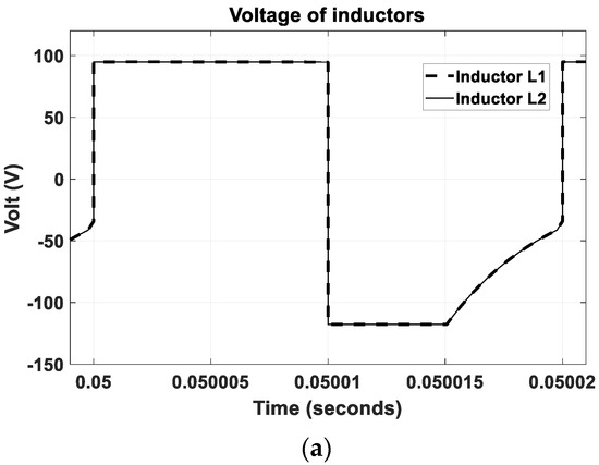
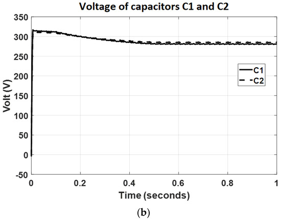
Figure 18.
Voltage waveforms across inductors (a) and capacitors (b) in the proposed boost converter.
According to Equation (5), the voltage across capacitor by considering and is predicted to be close to 288 VDC in the ideal working state and without considering the voltage drops and power losses across the components. Since the average voltage drop across inductors and is zero in a switching time period, a similar voltage is obtained across capacitor .
The state of the currents for the inductors in the QZSI circuit is shown in Figure 19a. This figure shows that for the power values between 200 and 400 W, a maximum value of 20 A and a minimum value of 10 A is established through these inductors. Currents with fewer amplitudes can be obtained by the application of larger inductors. Figure 19b,c present the state of the current for the same inductors and with 300 and 400 µH inductivity, respectively. In addition, the voltage across capacitors and is presented in Figure 19b. The same form of the current waveforms with the same amplitude is obtained for these capacitors. The voltages across switches and are shown in Figure 20. The state of the switches guarantees that in any time interval only one of these transistors is activated. In addition, the amplitude of the voltage across the drain and source pins of these transistors is related to the input voltage, output voltage, and modulation index that is more than . The reason for this value for the is the desired voltage amplitude at the load side that should be around 311VAC and 220 volt root-mean-square (RMS).
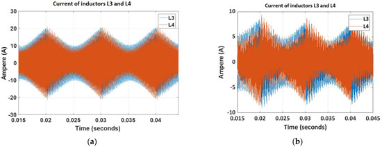
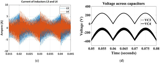
Figure 19.
(a–c) Currents of inductors and ; (d) voltage waveforms across capacitors in the proposed QZS converter.
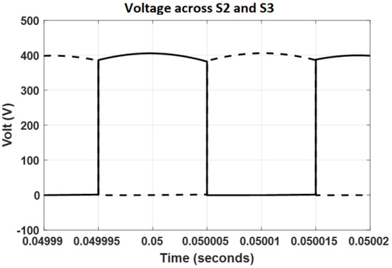
Figure 20.
Voltage waveforms across the switches and in the proposed QZS converter.
The voltage waveforms for the transistors in the FBI circuit are shown in Figure 21a,b. One of the most important results is shown in these two figures. The maximum side of the output voltage is supplied by the pair, and the minimum and negative side of the output voltage is prepared by the transistor pair. It is important to carefully observe the sequence of the generated voltages by these pairs and see that for the time intervals that the pair is generated, the positive side of the sinusoidal voltage of the generated voltage by the is zero. When the pair generates the negative side of the output sinusoidal voltage, no voltage is generated by the pair. The final state of the output voltage with the present sinusoidal state is shown in Figure 21c, and the current waveform is presented in Figure 21d. The quality of the generated voltage and currents is considerable. The RL type of the loads is selected to behave as the real state of the loads, and in order to be comparable with the laboratory test results, the amount of the R and L are selected as 200–400 W and 50 VAR, respectively. Figure 21e,f show the output voltage and current waveforms for a heavier load. For that, a similar RL load is connected across the first load at s, and the behavior of the voltage and current waveforms are investigated. As can be seen, no change including any type of undershoots or overshoots is obtained for the voltage, and current is doubled at s. To show the reaction of the proposed topology under resistive load, Figure 21g,h are presented. These two figures show the output current waves for the single and doubled resistive loads, respectively. Firstly, only one resistive load is considered, and then the second load equal to the first resistive load is added at s. These waves show that the current is simply doubled.
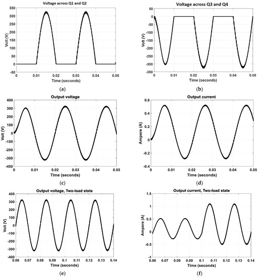
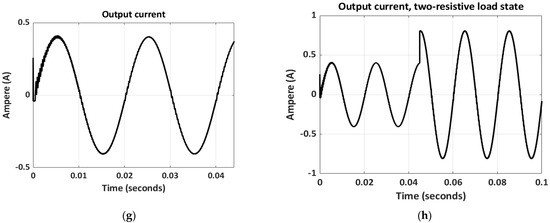
Figure 21.
Voltage waveform across the transistors: (a) ; (b) (c) output voltage; (d) output current in one-load (RL); (e) output voltage in two-load (RL) states; (f) output current in two-load (RL) states, (g) output current in one-load (R); (h) output current in two-load (R) states.
5. Experimental Results
A prototype circuit with all details presented in Table 3 was established in the laboratory, and some of the results are reported in this section. A 96 DV voltage at the input side of the step-up converter was established, and finally a sinusoidal output voltage was obtained across the load nodes with 50 Hz frequency and around 220 RMS. The amount of the inductors and capacitors and the power semiconductor devices are the same with the considered devices in the simulation. Figure 22 presents the test results.
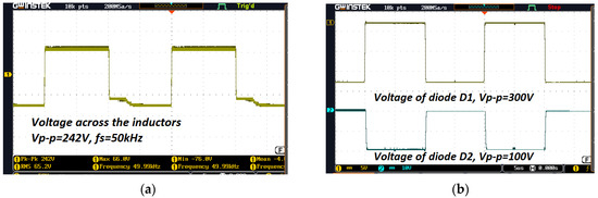
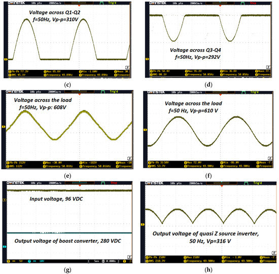
Figure 22.
Test results: (a) voltage of inductors L1 and L2; (b) voltages of diodes D1 and D2; (c) voltages across the transistors Q1–Q2; (d) Q3-Q4, output voltage under (e) resistive–inductive; (f) resistive loads; (g) input–output voltages of boost converter; (h) output voltage of quasi Z-source inverter.
Figure 22a presents the voltage across inductors L1 and L2 at the boost converter side. According to the simulation results, a peak-to-peak voltage around 240 V should be obtained for these inductors. Test results confirm the correctness of the simulation results. The switching frequency at the boost converter side is equal to 50 kHz. Another result is that both inductors are charged and discharged simultaneously according to the theoretical results. Figure 22b shows the voltage across two D1 and D2 diodes. This figure easily proves that these diodes are activated in two different time intervals and work in reverse. Adjustable probes are used, and the volume on the probes are set to show the real measured voltages; −300 and −100 volts are obtained across these diodes.
Two interesting results are obtained in Figure 22c,d, and the voltage across the switches Q1-Q2 and Q3-Q4 are reported. As expected, rectified voltage waves with maximum and minimum amplitude of the output voltage and 50 Hz frequency are obtained for these pairs of transistors. These voltages are considered as the input voltage for the full bridge inverter block, and finally a fully sinusoidal voltage is obtained for the load. These voltage waves are presented in Figure 22e,f for RL and R loads, respectively. As mentioned, the volumes on the probes are adjusted to show the actual measured values. This sine wave is obtained for a 200 W and 50 VAR RL load. In addition, the same working condition is tested for the 200 W resistive load. A pure sinusoidal voltage waveform is reported for this operational state.
Figure 22g presents the input and output voltages of the boost converter. The output voltage of the quasi Z-source inverter across capacitor C4 is shown in Figure 22h. A full rectified voltage with about 310 V amplitude is reported across this capacitor with 50 Hz of frequency. After hardware tests in the laboratory for a group of load with a power maximum to 400 W, the efficiency diagram of the converter is obtained and reported in Figure 23. To evaluate the performance of the proposed boost converter-based QZS inverter, the similar converter topologies are considered and reported. As a result of examining the efficiency performance of the proposed converter circuit, it was noted that the highest efficiency of the circuit is obtained for powers above 350 watts. Compared with other inverter circuits, the proposed inverter circuit performed above the average. These converter circuits are taken from articles published in the last 3 years.
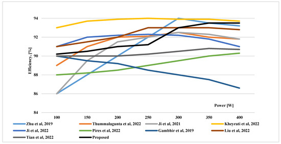
Figure 23.
Measured efficiency and comparison with similar topologies [42,43,44,45,46,47,48,49,50].
According to the results, for input power equal to 100 W, 200 W, 300 W, and 400 W, respectively, 9,8 W, 18 W, 21 W, and 26 W, were reported as the power losses. Theoretical analysis shows that the main sources of the power losses are the semiconductor devices, and the test results confirm the theory. The test results in Figure 24 show the distribution of the power losses for the devices at different powers.
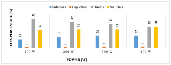
Figure 24.
Power loss distribution for elements of a converter.
According to this figure, the main source of the power loss is the power diodes, and the minimum loss is for capacitors. The power losses for the diodes for the higher current values in the circuit are smaller, while the losses for the inductors are greater. Results show that the power losses for the switches are more in accordance with increasing current values in the circuit.
6. Conclusions
A DC to AC power converter topology is presented in this study. The configuration of the proposed converter is preparing the circuit for low input voltage applications, such as the photovoltaic approaches. For that, at the first stage, this limited DC input voltage is enhanced through an optimized boost converter and then by the application of a modified quasi-impedance source inverter. A pair of positive and negative rectified AC voltage is obtained. At the final stage, these voltages are mixed in a full bridge inverter, and fully sinusoidal voltage is obtained for the load. For the boost converter, a switched-inductor block is used instead of the inductor, and the location of this component and power diode is changed. In comparison with a conventional step-up converter, not only is the gain of the converter increased, but also the ripples of the input current of the converter are decreased, which will obtain a more reliable converter topology with a longer lifetime of the input voltage source. On the quasi Z-source side, a pair of power transistors are used in the converter. Since the conventional Z-source inverters do not have any power semiconductor in their topology, the modified converter will have some advantages, such as the adjustable voltage gain on the output side of the converter in comparison with its input voltage. A modified sinusoidal PWM technique is used, and positive and negative voltages are formed at the output nodes of this block. Finally, a full bridge inverter simply mixed these voltages, and fully sinusoidal voltages are obtained at the load nodes. The presented topology can be used in different power classes and values.
Author Contributions
Conceptualization, H.T., A.H.M. and S.C.; methodology, E.A., A.H.M. and S.C.; software, H.T., A.H.M. and R.F.; validation, E.A., A.H.M. and S.C.; formal analysis, H.T., A.H.M. and R.F.; investigation, E.A., A.H.M. and S.C.; resources, S.C.; data curation, H.T., E.A., A.H.M., R.F. and S.C.; writing—original draft preparation, H.T. and R.F.; writing—review and editing, E.A., A.H.M. and S.C.; visualization, H.T., E.A. and A.H.M.; supervision, S.C.; project administration, H.T. and R.F.; funding acquisition, S.C. All authors have read and agreed to the published version of the manuscript.
Funding
This work was also funded by Geo-Informatics and Space Technology Development Agency (Public Organization): GISTDA.
Data Availability Statement
The datasets generated during and/or Analyzed during the current study are not publicly available due to [REASON(S) WHY DATA ARE NOT PUBLIC] but are available from the corresponding author on reasonable request.
Conflicts of Interest
The authors declare that they have no conflicts of interest to report regarding the present study.
References
- Zhang, S.; Xiang, Y.; Liu, J.; Liu, J.; Yang, J.; Zhao, X.; Jawad, S.; Wang, J. A regulating capacity determination method for pumped storage hydropower to restrain PV generation fluctuation. CSEE J. Power Energy Syst. 2020, 8, 304–316. [Google Scholar] [CrossRef]
- Pachauri, R.K.; Alhelou, H.H.; Bai, J.; Golshan, M.E.H. Adaptive Switch Matrix for PV Module Connections to Avoid Permanent Cross-Tied Link in PV Array System Under Non-Uniform Irradiations. IEEE Access 2021, 9, 45978–45992. [Google Scholar] [CrossRef]
- Alhuwaishel, F.M.; Allehyani, A.K.; Al-Obaidi, S.A.S.; Enjeti, P.N. A Medium-Voltage DC-Collection Grid for Large-Scale PV Power Plants with Interleaved Modular Multilevel Converter. IEEE J. Emerg. Sel. Top. Power Electron. 2020, 8, 3434–3443. [Google Scholar] [CrossRef]
- Lashab, A.; Sera, D.; Hahn, F.; Camurca, L.; Terriche, Y.; Liserre, M.; Guerrero, J.M. Cascaded multilevel PV inverter with im-proved harmonic performance during power imbalance between power cells. IEEE Trans. Ind. Appl. 2020, 56, 2788–2798. [Google Scholar] [CrossRef]
- Abdel-Rahim, O.; Wang, H. A New High Gain DC-DC Converter with Model-Predictive-Control Based MPPT Technique for Photovoltaic Systems. CPSS Trans. Power Electron. Appl. 2020, 5, 191–200. [Google Scholar] [CrossRef]
- Xu, S.; Shao, R.; Cao, B.; Chang, L. Single-phase grid-connected PV system with golden section search-based MPPT algorithm. Chin. J. Electr. Eng. 2021, 7, 25–36. [Google Scholar] [CrossRef]
- Riquelme-Dominguez, J.M.; Martinez, S. Systematic Evaluation of Photovoltaic MPPT Algorithms Using State-Space Models Under Different Dynamic Test Procedures. IEEE Access 2022, 10, 45772–45783. [Google Scholar] [CrossRef]
- Singh, N.; Gupta, K.K.; Jain, S.K.; Dewangan, N.K.; Bhatnagar, P. A Flying Squirrel Search Optimization for MPPT Under Partial Shaded Photovoltaic System. IEEE J. Emerg. Sel. Top. Power Electron. 2021, 9, 4963–4978. [Google Scholar] [CrossRef]
- Singh, K.A.; Prajapati, A.; Chaudhary, K. High-Gain Compact Interleaved Boost Converter with Reduced Voltage Stress for PV Application. IEEE J. Emerg. Sel. Top. Power Electron. 2022, 10, 4763–4770. [Google Scholar] [CrossRef]
- Kunjuramakurup, L.; Sulthan, S.M.; Ponparakkal, M.S.; Raj, V.; Sathyajith, M. A High-Power Solar PV-fed TISO DC-DC Converter for Electric Vehicle Charging Applications. Energies 2023, 16, 2186. [Google Scholar] [CrossRef]
- Mondzik, A.; Stala, R.; Pirog, S.; Penczek, A.; Gucwa, P.; Szarek, M. High Efficiency DC–DC Boost Converter with Passive Snubber and Reduced Switching Losses. IEEE Trans. Ind. Electron. 2022, 69, 2500–2510. [Google Scholar] [CrossRef]
- Niu, R.; Zhang, H.; Song, J. Model Predictive Control of DC–DC Boost Converter Based on Generalized Proportional Integral Observer. Energies 2023, 16, 1245. [Google Scholar] [CrossRef]
- Smadi, A.A.; Khoucha, F.; Amirat, Y.; Benrabah, A.; Benbouzid, M. Active Disturbance Rejection Control of an Interleaved High Gain DC-DC Boost Converter for Fuel Cell Applications. Energies 2023, 16, 1019. [Google Scholar] [CrossRef]
- Alajmi, B.N.; Marei, M.I.; Abdelsalam, I.; Ahmed, N.A. Multiphase Interleaved Converter Based on Cascaded Non-Inverting Buck-Boost Converter. IEEE Access 2022, 10, 42497–42506. [Google Scholar] [CrossRef]
- Chen, H.-C.; Lu, C.-Y.; Rout, U.S. Decoupled Master-Slave Current Balancing Control for Three-Phase Interleaved Boost Converters. IEEE Trans. Power Electron. 2018, 33, 3683–3687. [Google Scholar] [CrossRef]
- Gules, R.; Pfitscher, L.; Franco, L. An interleaved boost DC-DC converter with large conversion ratio. In Proceedings of the 2003 IEEE International Symposium on Industrial Electronics, Rio de Janeiro, Brazil, 9–11 June 2003; pp. 411–416. [Google Scholar] [CrossRef]
- Tseng, K.-C.; Huang, C.-C.; Shih, W.-Y. A High Step-Up Converter with a Voltage Multiplier Module for a Photovoltaic System. IEEE Trans. Power Electron. 2013, 28, 3047–3057. [Google Scholar] [CrossRef]
- Hu, X.; Gong, C. A High Gain Input-Parallel Output-Series DC/DC Converter with Dual Coupled Inductors. IEEE Trans. Power Electron. 2015, 30, 1306–1317. [Google Scholar] [CrossRef]
- Forouzesh, M.; Shen, Y.; Yari, K.; Siwakoti, Y.P.; Blaabjerg, F. High-Efficiency High Step-Up DC–DC Converter with Dual Coupled Inductors for Grid-Connected Photovoltaic Systems. IEEE Trans. Power Electron. 2018, 33, 5967–5982. [Google Scholar] [CrossRef]
- Rezaie, M.; Abbasi, V. Ultrahigh Step-Up DC–DC Converter Composed of Two Stages Boost Converter, Coupled Inductor, and Multiplier Cell. IEEE Trans. Ind. Electron. 2022, 69, 5867–5878. [Google Scholar] [CrossRef]
- Babaei, E.; Asl, E.S.; Babayi, M.H. Steady-State and Small-Signal Analysis of High-Voltage Gain Half-Bridge Switched Boost Inverter. IEEE Trans. Ind. Electron. 2016, 63, 3546–3553. [Google Scholar] [CrossRef]
- Kou, B.; Wei, J.; Zhang, L. Switching and Conduction Loss Reduction of Dual-Buck Full-Bridge Inverter Through ZVT Soft-Switching Under Full-Cycle Modulation. IEEE Trans. Power Electron. 2020, 35, 5031–5046. [Google Scholar] [CrossRef]
- Gui, Y.; Xu, Q.; Blaabjerg, F.; Gong, H. Sliding Mode Control with Grid Voltage Modulated DPC for Voltage Source Inverters Under Distorted Grid Voltage. CPSS Trans. Power Electron. Appl. 2019, 4, 244–254. [Google Scholar] [CrossRef]
- Anand, S.; Gundlapalli, S.K.; Fernandes, B.G. Transformer-Less Grid Feeding Current Source Inverter for Solar Photovoltaic System. IEEE Trans. Ind. Electron. 2014, 61, 5334–5344. [Google Scholar] [CrossRef]
- Li, H.; Zeng, Y.; Zhang, B.; Zheng, T.Q.; Hao, R.; Yang, Z. An Improved H5 Topology with Low Common-Mode Current for Transformerless PV Grid-Connected Inverter. IEEE Trans. Power Electron. 2019, 34, 1254–1265. [Google Scholar] [CrossRef]
- Liu, B.; Su, M.; Yang, J.; Song, D.; He, D.; Song, S. Combined Reactive Power Injection Modulation and Grid Current Distortion Improvement Approach for H6 Transformer-Less Photovoltaic Inverter. IEEE Trans. Energy Convers. 2017, 32, 1456–1467. [Google Scholar] [CrossRef]
- Tang, Z.; Su, M.; Sun, Y.; Cheng, B.; Yang, Y.; Blaabjerg, F.; Wang, L. Hybrid UP-PWM Scheme for HERIC Inverter to Improve Power Quality and Efficiency. IEEE Trans. Power Electron. 2019, 34, 4292–4303. [Google Scholar] [CrossRef]
- Bubalo, M.; Bašić, M.; Vukadinović, D.; Grgić, I. Hybrid Wind-Solar Power System with a Battery-Assisted Quasi-Z-Source Inverter: Optimal Power Generation by Deploying Minimum Sensors. Energies 2023, 16, 1488. [Google Scholar] [CrossRef]
- Loh, P.C.; Blaabjerg, F. Magnetically Coupled Impedance-Source Inverters. IEEE Trans. Ind. Appl. 2013, 49, 2177–2187. [Google Scholar] [CrossRef]
- Gajanayake, C.; Vilathgamuwa, D.; Loh, P.C. Small-Signal and Signal-Flow-Graph Modeling of Switched Z-Source Impedance Network. IEEE Power Electron. Lett. 2005, 3, 111–116. [Google Scholar] [CrossRef]
- Jeyasudha, S.; Geethalakshmi, B. Steady State Analysis in Continuous Conduction Mode of a Novel Z-Source Boost Hybrid Converter. In Proceedings of the 2018 International Conference on Recent Trends in Electrical, Control and Communication (RTECC), Malaysia, Malaysia, 20–22 March 2018; pp. 210–215. [Google Scholar] [CrossRef]
- Veerachary, M.; Kumar, P. Analysis and Design of Quasi-Z-Source Equivalent DC–DC Boost Converters. IEEE Trans. Ind. Appl. 2020, 56, 6642–6656. [Google Scholar] [CrossRef]
- Zhu, X.; Zhang, B.; Qiu, D. A New Half-Bridge Impedance Source Inverter with High Voltage Gain. IEEE Trans. Power Electron. 2019, 34, 3001–3008. [Google Scholar] [CrossRef]
- Tang, Y.; Xie, S.; Ding, J. Pulsewidth Modulation of Z-Source Inverters with Minimum Inductor Current Ripple. IEEE Trans. Ind. Electron. 2014, 61, 98–106. [Google Scholar] [CrossRef]
- Fang, X.; Tian, Y.; Ding, X.; Ma, B. Series-type switched-inductor Z-source inverter. CES Trans. Electr. Mach. Syst. 2020, 4, 53–60. [Google Scholar] [CrossRef]
- Zhu, M.; Yu, K.; Luo, F.L. Switched Inductor Z-Source Inverter. IEEE Trans. Power Electron. 2010, 25, 2150–2158. [Google Scholar] [CrossRef]
- Jagan, V.; Kotturu, J.; Das, S. Enhanced-Boost Quasi-Z-Source Inverters with Two-Switched Impedance Networks. IEEE Trans. Ind. Electron. 2017, 64, 6885–6897. [Google Scholar] [CrossRef]
- Nguyen, M.-K.; Duong, T.-D.; Lim, Y.-C.; Kim, Y.-G. Switched-Capacitor Quasi-Switched Boost Inverters. IEEE Trans. Ind. Electron. 2018, 65, 5105–5113. [Google Scholar] [CrossRef]
- Nguyen, M.-K.; Le, T.-V.; Park, S.-J.; Lim, Y.-C.; Yoo, J.-Y. Class of high boost inverters based on switched-inductor structure. IET Power Electron. 2015, 8, 750–759. [Google Scholar] [CrossRef]
- Zhu, X.; Zhang, B.; Qiu, D. A High Boost Active Switched Quasi-Z-Source Inverter with Low Input Current Ripple. IEEE Trans. Ind. Informatics 2019, 15, 5341–5354. [Google Scholar] [CrossRef]
- Raj, A. PMP-DC/DC Controllers, Application Report SLVA390A–February 2010–Revised March 2020, Calculating Efficiency; Texas Instruments: Dallas, TX, USA, 2020. [Google Scholar]
- Madzharov, N.; Hinov, N. Analysis and Design of Resonant DC/AC Converters with Energy Dosing for Induction Heating. Energies 2023, 16, 1462. [Google Scholar] [CrossRef]
- Thummalagunta, A.; Patne, N.R.; Kodandaram, N. Analysis and Control of Switched Quasi-Impedance-Source-Inverter with Superior Boosting Ability for Renewable Energy Applications. IEEE Trans. Ind. Appl. 2022, 58, 3783–3793. [Google Scholar] [CrossRef]
- Ji, Y.; Geng, L.; Li, F.; Liu, H. Active-Switched Coupled-Inductor Impedance Network Boost Inverters. IEEE Trans. Veh. Technol. 2021, 70, 319–330. [Google Scholar] [CrossRef]
- Kheyrati, M.R.; Rajaei, A.; Tehrani, V.M.; Mirzavand, G.; Shahparasti, M. A Three-Level Single Stage A-Source Inverter with the Ability to Generate Active Voltage Vector During Shoot-Through State. IEEE Access 2022, 10, 31788–31799. [Google Scholar] [CrossRef]
- Ji, Y.; Geng, L.; Li, F.; Liu, H.; Wheeler, P. An Enhanced-Boost Coupled-Inductor Impedance Network Inverter without Limitation of Inductor Parameters. IEEE Trans. Transp. Electrif. 2022, 8, 699–709. [Google Scholar] [CrossRef]
- Pires, V.F.; Cordeiro, A.; Foito, D.; Bondarenko, O. Fault-Tolerant Three-Phase VSI Based on a Modified Impedance Source Boost Inverter. IEEE Trans. Ind. Appl. 2022, 58, 4859–4872. [Google Scholar] [CrossRef]
- Gambhir, A.; Mishra, S.K.; Joshi, A. A Modified PWM Scheme to Improve Performance of a Single-Phase Active-Front-End Impedance Source Inverter. IEEE Trans. Ind. Appl. 2019, 55, 928–942. [Google Scholar] [CrossRef]
- Liu, P.; Xu, J.; Sun, M.; Yuan, J.; Blaabjerg, F. New Discontinuous Space Vector Modulation Strategies for Impedance-Source Inverter with Superior Thermal and Harmonic Performance. IEEE Trans. Ind. Electron. 2022, 69, 13079–13089. [Google Scholar] [CrossRef]
- Tian, Y.; Liu, T.; Wang, Y.; Yang, D.; Hao, Y.; Chen, Z. Virtual Impedance Refined Inductor Current Observation and Current Sensorless Control for Grid-Connected Inverter. IEEE Trans. Power Electron. 2022, 37, 10239–10249. [Google Scholar] [CrossRef]
- Nguyen, C.V.C.; Cha, H.; Van Bui, D.; Choi, B. Modified Double-Dual-Boost High-Conversion-Ratio DC–DC Converter with Common Ground and Low-Side Gate Driving. IEEE Trans. Power Electron. 2022, 37, 4952–4956. [Google Scholar] [CrossRef]
- Goyal, V.K.; Shukla, A. Two-Stage Hybrid Isolated DC–DC Boost Converter for High Power and Wide Input Voltage Range Applications. IEEE Trans. Ind. Electron. 2022, 69, 6751–6763. [Google Scholar] [CrossRef]


Disclaimer/Publisher’s Note: The statements, opinions and data contained in all publications are solely those of the individual author(s) and contributor(s) and not of MDPI and/or the editor(s). MDPI and/or the editor(s) disclaim responsibility for any injury to people or property resulting from any ideas, methods, instructions or products referred to in the content. |
© 2023 by the authors. Licensee MDPI, Basel, Switzerland. This article is an open access article distributed under the terms and conditions of the Creative Commons Attribution (CC BY) license (https://creativecommons.org/licenses/by/4.0/).