Abstract
Recently, there has been considerable research interest in the potential for DC distribution systems in buildings instead of the traditional AC distribution systems. Due to the need for performing power conversions between DC and AC electricity, DC distribution may provide electrical efficiency advantages in some systems. To support comparative evaluations of AC-only, DC-only, and hybrid AC/DC distribution systems in buildings, a new modeling toolkit called the Building Electrical Efficiency Analysis Model (BEEAM) was developed and is described in this paper. To account for harmonics in currents or voltages arising from nonlinear devices, the toolkit implements harmonic power flow, along with nonlinear device behavioral descriptions derived from empirical measurements. This paper describes the framework, network equations, device representations, and an implementation of the toolkit in an open source software package, including a component library and graphical interface for creating circuits. Simulations of electrical behavior and device and system efficiencies using the toolkit are compared with experimental measurements of a small office environment in a variety of operating and load configurations. A detailed analysis of uncertainty estimation is also provided. Key findings were that a comparison of predicted versus measured efficiencies and power losses in the validation testbed using the initial toolkit implementation predicted device- and system-level efficiencies with reasonably good accuracy under both balanced and unbalanced AC scenarios. An uncertainty analysis also revealed that the maximum estimated error for system efficiency across all scenarios was 3%, and measured and modeled system efficiency agreed within the experimental uncertainty in approximately half of the scenarios. Based on the correspondence between simulation and measurement, the toolkit is proposed by the authors as a potentially useful tool for comparing efficiency in AC, DC, and hybrid AC/DC distribution systems in buildings.
Notation: In this paper, bold letters are used to denote matrices or vectors; non-bold letters are used for scalar quantities; subscripts are used to index device, port, or harmonic numbers; denotes the set of whole numbers; , denotes the space of continuous functions with first k derivatives; represents the matrix transpose operator; symbolizes the absolute value of a real number or cardinality of a set; denotes a phasor quantity; and symbolize the real and imaginary parts of a complex number, respectively; represents the magnitude of a complex number; denotes complex conjugation; ; symbolizes the evaluation of function f with input variable(s) x and fixed parameter(s) .
1. Introduction
In recent years, there has been considerable interest in comparing the efficiency of DC distribution systems and traditional AC distribution systems. This interest is inspired by increasing proportions of residential electrical loads, miscellaneous electrical loads (MELs) [1,2], and building equipment which can operate from DC distribution systems. In addition, many renewable power generation systems, such as solar photovoltaic (PV) and energy storage systems, natively produce DC power, enabling a direct connection between DC sources and loads. Use of DC distribution reduces or eliminates conversions between AC and DC, and therefore, frequently has been proposed as a means of achieving energy savings [3,4,5,6,7,8,9].
Electrical distribution systems in buildings are similar in concept to electrical distribution systems in utilities [10,11]. However, distribution systems in buildings cannot be conveniently analyzed using conventional grid-power-flow techniques because building distribution systems’ loads are typically composed of large proportions of nonlinear devices [12]. In addition, quantifying the efficiency and energy costs of competing distribution system topologies (including AC-only, DC-only, and hybrid AC/DC) can be challenging because of the number of possible electrical configurations, how system boundaries are defined, whether the application includes on-site storage and/or solar PV, combinations of potential loads and equipment types, and the efficiencies of the converters used [12,13,14,15]. Modeling and simulations provide means of estimating and comparing electrical distribution systems’ performances, and several such approaches have been proposed. Nearly all studies performed have used some form of energy-balance model, in which loads and component losses are tallied to estimate the required input energy. The simplest of these use basic system topologies and fixed device efficiencies to estimate the potential energy savings of a DC distribution compared to an AC one [3,5,16,17]. Other early energy-balance models used closed-formed equations to compute converter, transformer, and wiring losses under a variety of scenarios [18,19]. More recent energy-balance models account for performance in partly-loaded conditions by including multiple scenarios or time-series load profiles and using efficiency curves or tables to model varying converter efficiencies [6,20,21]; some studies also estimated wiring losses using various approximations [9,14,22]. Apart from energy-balance models, one study used a modified version of optimal power flow to model mixed AC-DC building electrical distribution systems [12], and one used time domain simulation to model a low-voltage DC distribution [23].
Energy-balance models share a common shortcoming: they do not directly model voltage, current, and power flows within the distribution network. Therefore, they do not generally provide other measures of system performance (voltage drop, power quality, and the like) and may also yield inaccurate estimates of efficiency to the extent that device losses are influenced by phenomena such as voltage, system imbalance, and current distortion. To address this shortcoming, the authors are developing next-generation building modeling tools to provide a flexible and modular environment to enable practitioners to assess and compare the energy efficiencies and lifecycle costs of competing electrical network designs.
A key component of this research is the development of a modeling approach for estimating electrical efficiency in building distribution systems without the need for detailed time-domain simulations, which require prohibitively long computational times for large systems. However, because of nonlinearities and harmonic content arising from electronic devices in most modern buildings, linear circuit-analysis approaches are generally not valid for assessments of these electrical efficiencies.
In [24], the authors compared and contrasted three modeling approaches for estimating efficiencies in AC-only, DC-only, and hybrid AC/DC distribution systems: energy balance based on device efficiency curves, harmonic power flow (HPF), and full time-domain simulation. Therein, the comparison between modeling results and experimental measurements supported the conclusion that the HPF method provides a suitable balance among accuracy, computational time, and model development time compared to the other approaches. In addition, the HPF method provides the advantages of predicting harmonic content, simulation of highly unbalanced loading conditions, and scalability for simulating large networks [25,26].
This paper expands upon the research in [24] by providing a detailed description of the underlying framework and implementation used to model a system of nonlinear network equations representing modern buildings, packaged in a new software tool called the Building Electrical Efficiency Analysis Model (BEEAM) [27]. Specifically, the paper describes how the system network equations required for HPF are constructed by representing all devices as one- or two-port networks, which may include nonlinear devices. An implementation of the toolkit in Modelica is also described, including an overview of the toolkit component library and graphical interface. Simulations of electrical behavior and device and system efficiencies are also compared with experimental measurements of a small office in different configurations and with various loads. The validation presented in this work stands in contrast to the earlier DC-distribution-system-modeling literature, which has very rarely compared simulation results to real experimental data or field measurements.
Key contributions of this work are:
- Description of a framework and modeling approach for assessment of component and system electrical efficiencies in AC, DC, and hybrid AC/DC distribution configurations, including nonlinear effects and potential load imbalances, which do not rely on time-domain simulations;
- Proposal of a new software tool that implements the above approach to perform detailed DC vs. AC distribution-efficiency comparisons;
- Initial validation of the tool’s accuracy with experimental measurements, for several circuit configurations and power levels in both AC and DC distribution systems, including balanced and unbalanced load conditions.
The remainder of this paper is structured as follows. Section 2 provides a description of the overall framework used to model electrical networks and the general harmonic power flow solution. This is followed in Section 3 by a description of component models for linear and nonlinear devices. Implementation of the modeling toolkit in software is described in Section 4. Section 5 describes experimental validation of the toolkit using laboratory measurements; a detailed uncertainty analysis is contained in the Appendix A. Finally, conclusions and suggestions for future research are provided in Section 6.
2. Modeling Framework
This section describes the modeling framework used to estimate harmonic currents, voltages, and power flows in buildings within the BEEAM modeling toolkit. Background on electrical network theory using one- and two-port models is first given, followed by a description of the model representations of several devices.
2.1. Background on Linear AC Circuit Analysis
Steady-state analysis of AC circuits using frequency-based methods is a well-established technique in the power engineering community. In electrical systems composed of linear and passive circuit elements, driven by sinusoidal sources, phasor analysis is often employed to reduce the solution of steady-state currents and/or voltages in a network to solving a system of linear algebraic equations. In this method, sinusoidal voltage and currents are represented as phasors in the frequency domain under the transform:
where f can represent voltage or current, is the phasor representation of f, is the root-mean-square (rms) value of f, is the angular electrical frequency, t is time, symbolizes , and is a phase shift generally measured with respect to an input source. On the right side of (1), the symbol for electrical frequency is suppressed but implied under the transformation shown. Additionally, note that the representation of the phasor magnitude as the rms value of f (versus peak value) is arbitrary but is the convention used throughout this paper.
In phasor analysis, the steady-state effect (reaction) of an inductive element L in an electrical circuit represented by an inductive reactance, , and the capacitive element C by capacitive reactance, . Resistive elements do not have frequency dependence and therefore are not transformed under phasor analysis. Impedance is a complex number with total resistance R and total reactance X. These quantities may consist of combined resistances, inductive reactances, and capacitive reactances, computed according to network circuit laws.
Let denote a vector of phasors containing phasor voltages at nodes in an electrical network. denotes a vector of phasors containing phasor currents , through branches in the network. Let denote an impedance matrix which specifies the network impedance relations between node voltage and branch current phasors, i.e., . For a linear network, the solution of steady-state current phasors can be computed (assuming is invertible) as:
where is called the admittance matrix. Although phasor analysis in power engineering is generally applied at one frequency (e.g., line frequency of the voltage source), under the assumption of system linearity, (2) can be applied at any frequency to determine an overall steady-state response. Letting denote the harmonic number with respect to base frequency , phasors corresponding to voltages and currents with electrical angular frequency can be transformed by generalizing (3) as:
where is the root-mean-square (rms) value of f at harmonic h, is the implied angular electrical frequency of phasor , and is the phase shift at this harmonic number. Note that while (i.e., DC) is valid in (3), there is no phase shift, and the term is omitted.
Let , be a set of harmonic numbers which are to be evaluated, where herein it is assumed that . The solution of the linear network equations at each harmonic h can be computed individually by generalizing (2) by the use of (3) as:
where is the admittance matrix at harmonic h. While the solution given by the phasor approach in (4) is simple to implement, the method can unfortunately not be used in applications where there are nonlinear relationships between system voltages and currents, such as electrical systems containing typical electronic devices. Following the discussion below on one- and two-port network theory, the solution of these systems using harmonic power flow is discussed (see Section 2.3).
2.2. Electrical Network Theory
2.2.1. One- and Two-Port Network Representations
A two-port network, depicted in Figure 1, is an electrical network with two “ports”, each consisting of two terminals (four terminals total). The voltage/current relationships between the terminals are described using matrices: the two voltages and two currents are state variables, two of which are considered independent (or input) and two of which are considered dependent (or output) [28]. Note that in this context, “input” and “output” are defined for computational purposes only and do not necessarily indicate the direction of real power flow. Herein, port 1 (port 2) is arbitrarily assigned the input (output) port label.
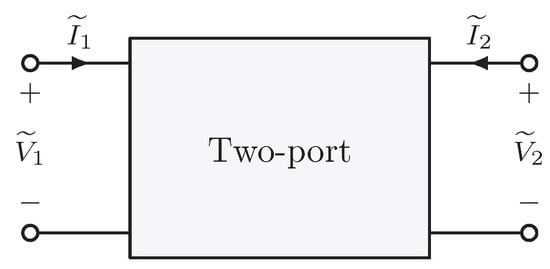
Figure 1.
General two-port network.
The “ABCD” representation is a common representation of a two-port network; this representation for the device in Figure 1 is given as:
In linear devices, coefficients A, B, C, and D in (5) are generally complex constants. Note that in this formulation, a positive (negative) sign indicates that current is flowing into (out of) the device; this convention explains the negative sign of in (5). See [29] for other equally-valid network representations.
To account for additional harmonics, the two-port matrix representation can be extended to represent harmonic voltage and current relationships. This is done by expressing the voltages and currents as vectors of phasors at each harmonic frequency (including for DC). To do this, let and represent the current and voltage phasors, respectively, for device d, at port and harmonic h. A, B, C, and D then become submatrices. For example, to relate input with output , define matrix element , in which is the harmonic order associated with the input phasor and h is the harmonic order associated with the output phasor, and define the sasme for matrix elements , , and . The two-port input/output relationship is for all harmonics is then given as:
Note that for purely linear devices (such as a cables), there is no cross-coupling of harmonics, and all off-diagonal elements of the submatrices are zero:
in which case the two-port representation is fully decoupled by a harmonic and can be written compactly as:
Nonlinear devices, however, may contain coupling between harmonics. Furthermore, the governing equations for practical nonlinear devices cannot always be described using the standard two-port network form. (The matrix elements themselves may be functions of the state variables, or the matrix representation may not be an adequate way to capture the nonlinear relationships.) To generalize the two-port network concept for nonlinear devices, a general nonlinear two-port network model for any arbitrary device is proposed herein which satisfies the following properties:
- The model specifies voltage phasor variables ( and ) and current phasor variables ( and ), ;
- The model defines a set of exactly independent nonlinear equations in the variables above that describe the device’s behavior;
- The nonlinear equations that define the device’s behavior can be written to describe exactly two independent variables and two dependent variables at each harmonic h.
Note that with these properties, a linear two-port network is a specific case of the general nonlinear two-port network model defined above. The network formulation used in this research also utilizes one-port networks for sources and loads, see Figure 2, which have a single voltage, a single current, and a (linear or nonlinear) relationship between them. A one-port network consists of H phasor voltage variables, H phasor current variables, and independent (linear or nonlinear) equations that can be written such that there is one independent and one dependent variable at each harmonic h.
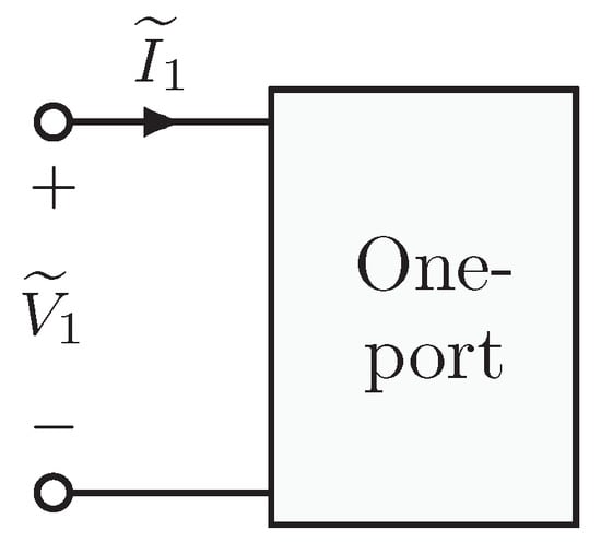
Figure 2.
General one-port network.
2.2.2. Defining Network Topologies
A distribution network can be viewed as a set of subgraphs formed by interconnecting network ports with ideal interconnects; this is the framework for how devices and distribution systems are modeled in this research. In this approach, each subgraph links at least two network ports, and each network port forms an "edge" in the subgraph. The subgraphs are related (coupled) to each other indirectly via the relationships defined by the one- and two-port networks.
Figure 3 demonstrates an example of an electrical network described in this fashion. The network depicted in Figure 3 could represent an ideal voltage source (device ) connected to a transformer () that in turn feeds two rectifiers (, ) serving resistive loads (, ).
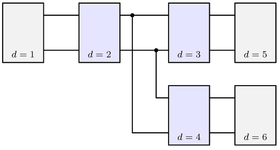
Figure 3.
Exemplary electrical network containing interconnected devices, wherein each device is depicted as a one-port (gray) or two-port (blue) network.
Figure 4 is a directed graph representation of the network of Figure 3, demonstrating how the network is decomposed into four directed subgraphs linked indirectly via the one- and two-port network equations for devices (subgraphs and ), (subgraphs and ), and (subgraphs and ). In Figure 4, represents port p of subgraph g, and represents edge k of subgraph g.
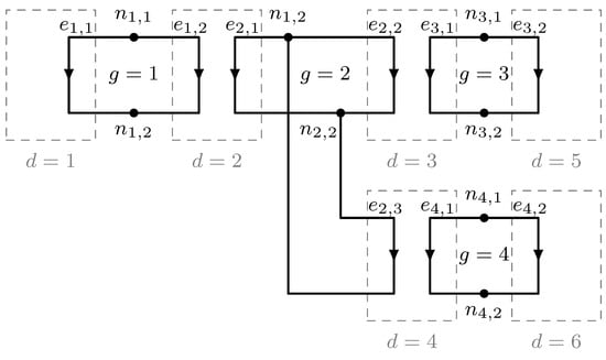
Figure 4.
Directed graph representation of the electrical network of Figure 3.
In an electrical network, the total number of variables is twice the number of edges (branches): one voltage and one current per edge [29]. Let E represent the total number of edges; the number of variables is then . (Note that for simplicity, harmonics are not yet being considered; see below for treatment of harmonics.) Note that the number of edges, E, is also equivalent to the total number of ports defined by the devices, since each edge is also a port. That is, , where and . Assuming that the system has a unique solution, independent equations must be defined to represent the system.
For any given subgraph g, there exists independent Kirchhoff’s voltage law (KVL) equations and independent Kirchhoff’s current law (KCL) equations, for a total of linear KVL and KCL equations [29]. For all subgraphs (i.e., the network as a whole), there are therefore E linear KVL and KVL equations. To fully define the system, another E equations are needed; these are obtained from the "connection equations" defined by the one- and two-port networks: V equations for the one-port networks and equations from the two-port networks. Since , the equations are thus obtained.
However, note that it is not typically necessary to obtain all equations to fully solve a system. For any given subgraph, the circuit state can be fully represented by node voltages or loop currents. This means that the entire network could be represented by node voltage state variables (for instance); the remaining voltages could be derived via KVL and the currents then solved via the connection equations and KCL. In practice, what this means is that the system of equations can generally be reduced to a smaller system of equations via substitution.
When considering harmonics, there are total variables, total equations from KVL and KCL, and variables from the one- and two-port network connection equations. Using node voltages phasors as state variables, a carefully selected set of equations involving those voltages could be used to define the system.
To illustrate the concepts in the foregoing, suppose the circuit in Figure 3 is to be solved for the set of harmonics . As shown in Figure 4, the system has edges across the four subgraphs, for a total of variables. There are one-port and two-port devices in the system. The required number of equations to solve the system is obtained from the:
- KVL equations: H from subgraph , from subgraph , H from subgraph , and H from subgraph ;
- KCL equations: H from each of the four subgraphs;
- connection equations from one-port devices;
- connection equations from two-port devices.
The total number of equations obtainable from the network is therefore 54. However, note that by defining node voltage phasors, a solution to the network states could be theoretically be obtained. Therefore, in this example, the number of simultaneous equations needed to solve the system is no more than 54 and could be as few as 12 (using variable substitution).
2.3. Harmonic Power Flow Solution
The solution of a set of generally nolinear equations representing an arbitrary electrical network is created in the modeling toolkit by employing a harmonic power flow (HPF) approach. The HPF method extends the traditional power flow methodology in three key aspects: (i) representation of additional harmonic frequencies beyond the fundamental (line) frequency in the system state; (ii) representation of the nonlinear behavior of all devices in the system, including individual harmonic contribution and potential cross-coupling; and (iii) enforcement of power balance at all harmonics [12,25].
In networks containing power-electronic converters or other nonlinear circuit elements, current into nonlinear device d, at port and harmonic h, is specified in the HPF method by a generally nonlinear, complex-valued function:
where is the set of all nonlinear devices in the system; is the average real power into device d, at harmonics , which is computed as:
where is the voltage and the input current of device d, for port 1 and harmonic h, respectively; in (9) is a vector of phasor currents into port at device d, at harmonics , in addition to possibly other harmonic current phasors in the network:
where , is device d’s input current at harmonic and is a vector of currents in the network that do not include any currents in the top portion of the vector in (11), or ; in (9) is a set of voltage phasors including at least the voltage for device d, port 1, and harmonic h, but possibly others in the network:
where is the device d, port 1 voltage at harmonic h, and is a vector of voltages in the network other than ; finally, the vector in (9) contains the device-specific behavioral parameters. The interpretation of (9) is that the h’th harmonic of the current phasor into device d at port is generally a function of: (a) the harmonic number h itself, (b) the device’s real input power, (c) currents into the device at other harmonics (), possibly other currents in the network at any harmonic (d), voltage harmonics at port of the device and possibly other nodes in the network, and (e) device-specific parameters, e.g., control settings, physical parameters, and device loading.
Solution of the network equations using HPF is accomplished using an iterative numerical procedure (e.g., Newton Raphson) to obtain convergence of all states at all specified harmonics within a specified threshold, while explicitly enforcing power balance throughout the network. In particular, the method includes the following steps:
- Initialize all network voltages and currents. For example, set the magnitudes and phase angles of all voltage and current phasors to zero, except known phasor voltage at ports of the voltage input source(s).
- Compute network currents. Using the last converged solution of network voltage phasors, compute current phasors through all branches of the network using either linear circuit analysis or (9) for all linear and nonlinear devices in the network, respectively.
- Enforce power balance. For each nonlinear device, compute the average real input power into the device—. Set or compute (if not known) the average real output power () of the device. Using the loss function for the device (see Section 3.5), adjust the magnitudes of the current phasors at the input port of the device so that power balance is achieved.
- Update network voltages. Using the adjusted currents in step 3, update all node voltage phasors in the network.
- If not converged, return to step 2.
The following section describes how network devices are modeled, including how nonlinear device behavior and losses are represented in the modeling framework.
3. Device Models
This section illustrates example linear and nonlinear device models for specific component types, focusing on those used in the validation studies in Section 5. In each case, the models below define connection equations for each device; exactly two of the four voltage and current phasors at each harmonic can be considered independent, and the other two are dependent.
3.1. Series Impedance
Consider a series impedance component, with impedance , where R is the resistance and X is the reactance at the fundamental () frequency harmonic. The following relationships apply:
The ABCD matrix of the series component for any harmonic is therefore:
3.2. Shunt Impedance
In a shunt impedance, the network equations are:
and the ABCD matrix of the shunt impedance for any harmonic is:
3.3. Constant Power Loads
Constant power loads (CPLs) are modeled as one-port components that absorb a fixed amount of real and reactive power to enforce the relation:
where is the total input harmonic apparent power, is the total average real power into the device given in (10), and
is the total reactive power into device d, for port and harmonic h. In the toolkit, users specify the components of the real and reactive harmonic power contributions in the summations in (10) and (18).
3.4. Transformers
This section defines single-phase and three-phase transformer models compatible with the proposed HPF algorithm. The models defined here neglect changes in resistance at harmonic frequencies due to the skin effect nonlinearity due to magnetic saturation and cross-coupling between phases. However, incorporation of these effects is theoretically possible and is suggested as future work.
3.4.1. Single-Phase Transformers
Single-phase transformers can be modeled as two-port devices. The most general representation of the single-phase transformer, allowing for nonlinear effects such as magnetic saturation, would require a general nonlinear two-port network model, as discussed in Section 2.2. In cases where nonlinear effects can be neglected, in addition to winding and magnetic core impedances, the ideal transformer model with voltage ratio (primary winding turns:secondary winding turns) shown in Figure 5 is used.
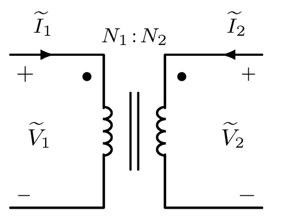
Figure 5.
Ideal single-phase transformer model.
The ABCD matrix representation for this ideal transformer component at any harmonic is:
where . A higher-fidelity model of the single-phase transformer which includes winding and magnetizing impedances, but neglects nonlinear effects, is shown in Figure 6. Note that the transformer model in Figure 6 is a composite model, utilizing series and shunt impedance elements and the ideal transformer.
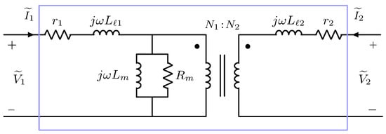
Figure 6.
Equivalent steady-state circuit for a single-phase transformer. The blue box defines a two-port component.
In Figure 6, are the resistances of winding 1 and 2, respectively; are the leakage inductances of winding 1 and 2, respectively; are the magnetizing inductance and resistance of the core, respectively; is the fundamental radial electrical frequency of the input. The internal circuit with boundaries defined by the blue box in Figure 6, represents a linear two-port network with the following an ABCD matrix valid for any harmonic:
where , , and .
3.4.2. Three-Phase Transformers
Three-phase transformers can be viewed as multi-terminal devices, as depicted in Figure 7. The most general representation of the device would include nonlinear effects such as magnetic saturation, differences in electrical parameters, and voltage imbalances; these non-idealities would generally lead to cross-coupling between harmonics between all phases and would require the use of a general nonlinear two-port network model. However, under certain assumptions (see below), it is possible to represent the device as a set of linear and uncoupled two-port devices.
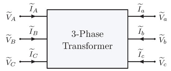
Figure 7.
Three-phase transformer component.
Suppose that the voltages and currents on the right side (analogous to a “port”) of the component in Figure 7 are known, and the voltages and currents on the left side are unknown; six equations are therefore needed to solve for the unknowns. Assuming the device is operating in the linear magnetic region (i.e., not magnetically saturated), there is symmetry of electrical transformer parameters among phases, and the three-phase voltage and current are balanced, each electrical phase of the transformer can be represented in steady-state as three separate circuits, with the two-port transformer models shown in Figure 6. In this way, two of the unknown variables can be solved in each of the three circuits, yielding the required six unknowns. An example two- and one-port representation of a balanced network illustrating this concept is shown in Figure 8.
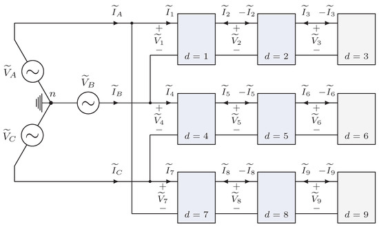
Figure 8.
Balanced electrical network with two-port linear transformer models.
In Figure 8, the network represents a three-phase utility voltage supplying a -Y connected building transformer with balanced loads across its three output windings. In this case, devices are represented by the two-port transformer models shown in Figure 6; devices and are two- and one-port devices, respectively. The numbering convention of voltages and currents is assigned arbitrarily; in this case, and are the voltage and current inputs (outputs) of the electrical phase transformer winding. Figure 8 also illustrates how network connections can result in a smaller number of system unknowns, as discussed in Section 2.2.2; for example, in this case, the output current of device is the (negative) input current into device .
If nonlinear effects are neglected but it cannot be assumed that the transformer’s parameters are electrically symmetric and/or there are voltage imbalances, then there will generally be coupling of harmonics between phases. In this case, the transformer can be represented by modification of the general two-port network matrix in (6). In particular, the set of input/output voltage vectors in (6) must both be augmented to include variables for the additional (third) winding on each side of the transformer.
3.5. Power-Electronic Converters
Power-electronic converters are generally nonlinear devices, requiring the use of generalized nonlinear component models. The following sections describe nonlinear device behavior, loss representation, and power balance for converter components commonly found in building applications and that can also be represented as two-port models. The following descriptions correspond to the single-phase converters for the hardware validation studies in Section 5; multi-port converter models (e.g., three-phase converters) are not described in this paper and are recommended for future work.
3.5.1. Converter Device-Specific Behavior
The parameterized, device-specific behavior function in (9) is a generally nonlinear function which describes the behavior of the input current through device d, as a function of harmonic number, the device’s input voltage and power, and possibly other bus current and voltage harmonics in the system. The vector contains parameter information specific to the device.
Several approaches can be used to determine the form and best-fit parameters for so that they can be used in an HPF algorithm, subject to the restriction that . The first step is to determine the general form of the function from measured or simulated time-domain device behavior, under a range of device input or output power values. Typically, observation readily indicates which variables most impact current magnitude and phase angle (see example below). Proceeding further, one may use several general approaches to functionally describe the behavior; e.g.,:
- (1)
- Empirical method: Using measured or simulated current waveforms, express as an dimensional surface, where n is the number of variables determined heuristically to influence current behavior. (In this work, as described below.) Express the surface function using a dimensional lookup table and use the linear interpolation between measured (simulated) points. Note that linear representation of the function ensures .
- (2)
- Analytical method: Again, using measured (simulated) current waveforms, express as a closed-form function in , in terms of an unknown parameter set. Using a nonlinear numerical optimization method, determine the best-fit parameters which minimize a distance metric of the error between predicted and measured (simulated) current magnitudes and phase angles (cf. [30]).
In the validation studies described in Section 5, the empirical method was used to determine . Therein, experimental observation indicated that the current magnitude for the devices under study were most influenced by the harmonic number h and device input power . (We observed that the input voltage waveform shape has little practical influence the current waveform for low levels of voltage distortion; the selected model therefore neglects its effects.) Figure 9 and Figure 10 show surface plots of the current magnitude and phase angle, respectively, of a power-electronic converter (Power Supply 3; see Section 5).
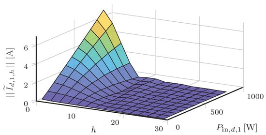
Figure 9.
Contour plot of the current magnitude of the measured nonlinear device as a function of harmonic number and input power.
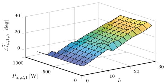
Figure 10.
Contour plot of the measured current phase angle of the nonlinear unwrapped device as a function of harmonic number and input power.
As shown in Figure 9, the magnitude of the measured current harmonics can be described as a reasonably smooth function of harmonic number itself and input power. Figure 10 indicates that the current phase angle can be reasonably approximated as a linear function of harmonic number only. Note that although the empirical method was used in this initial work, current research by the authors is investigating the analytical method for determining the device-specific behavioral function (see discussion on future work in Section 6).
3.5.2. Converter Loss Modeling
To enforce power balance for nonlinear devices in the network, it is necessary to model and characterize device losses. The average real power into device d, measured at port , , is given in (10). The average real power out of device d, measured at port , denoted , is given as:
The relationship between average real input power, output power, and power losses used herein expands upon the work in [20,31] and is expressed in the form:
where is the average real power loss in the device, is a loss function, and vector contains the three scalar loss parameters for the device: .
Currents injected into the power distribution system by AC-connected power electronic converters at harmonic frequencies () cause losses elsewhere, such as resistive losses in cables and in transformer windings and magnetic losses in transformer cores. In effect, converters transfer some power from the fundamental frequency to harmonic frequencies, such that (in an AC-input device, for example) the power transfer at port 1 is positive for but may be negative for . This power injected back to the distribution system at port 1 must be accounted for in each converter’s power balance equation (Equation (22)), which is why and are defined as summations across all harmonics.
Use of (22) with fitted parameters has been shown to yield reasonable accuracy when compared to measurements for a variety of devices (cf. [20,31]). However, the model suffers from the drawback of not adequately representing the power relationship at low power levels for some devices; for example, this discrepancy can arise if the device enters a "stand-by" or power-saving mode. To account for this behavior, this research proposes a "two-state" power loss function expressed as:
where is the stand-by power of device d; the scaling parameter is
where is the minimum measured output power of the device when it is not operating in stand-by mode; vector are the fitted loss parameters for the function in (22) after removing measured power values less than . Assigning and collecting parameters in vector , the power relationship for the nonlinear devices is expressed:
Herein, denotes the modified two-state power relationship, with adjusted loss parameters , for all devices . The best-fit loss parameters may be determined using a numerical fitting procedure to minimize the error between measured and predicted power loss according to (25).
In this work, we used linear least-squares to obtain best-fit parameters for each converter using input and output power observations at 10% steps from 10% to 100% rated power. Separately, we set equal to the converter’s observed power consumption when unloaded, as described above. An example curve fit for an AC/DC converter (Power Supply 1 in Section 5) is shown in Figure 11.
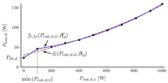
Figure 11.
Comparison of two-state loss model (blue, solid) to an uncorrected loss model (dashed, red); power loss measurements are shown as black dots.
As shown in Figure 11, power-loss measurements (black dots) at output power values less than W did not fall along the same polynomial curve as measurements at higher power levels. Therefore, the curve obtained from in (22) using best-fit parameters with all measurement points (red dashed line) resulted in noticeable discrepancies at low power levels. On the other hand, using the fitted curve in (23), the error in the modeled loss was improved, particularly at low power levels.
3.5.3. AC/DC Converters
To model AC/DC converters (“rectifiers”), power balance and internal loss modeling were calculated in this research using (9)–(10) and (21). Since these are nonlinear devices, harmonic currents on the input side of each component (designated as port below) are computed from (9). In the validation studies shown in Section 5, a simplified form of (9) was used; i.e., was assumed to be a parameterized function of harmonic number, output power, and fundamental input current only (neglecting the potential contributions of other network current and voltage harmonics), which can be written as:
In addition, there are three constraint equations for the rectifier: the DC input current is zero (), the DC output voltage is regulated (), and the AC output voltage is zero (). Thus, the rectifier component specifies one equation for power balance, equations for input current, one equation for the input DC current constraint, and H equations for the output voltage constraints, yielding equations in total. Moreover, the equations have been specified such that for each harmonic h there are exactly two independent variables and two dependent variables.
Note that for AC/DC converters with multiple DC output ports (see “central converter” in Section 5.1), the device is modeled herein as a rectifier coupled to multiple, isolated DC/DC converters. This device is therefore represented as a set of interconnected two-port networks, where the internal connections are simplified in the modeling framework to reduce the number of variables.
3.5.4. DC/DC Converters
As for AC/DC converters, port is designated as the input port and port as the output port. DC/DC converter losses are modeled using (25). In addition, DC/DC converters have the following constraints: AC input current is zero (), DC output voltage is regulated (), and AC output voltage is zero (). This yields one equation for power balance, equations for the AC input current constraints, and H equations for the output voltage constraints, for a total of equations.
3.5.5. DC/AC Converters
DC/AC converters (“inverters”) are modeled as voltage-source devices with a regulated (fixed) output voltage spectrum: and . (For a perfectly regulated inverter without switching harmonics, and .) Inverter losses also follow (25). Finally, inverter AC input current is zero (). This yields one equation for power balance, equations for the AC input current constraints, and H equations for the output voltage constraints, again for a total of equations.
4. Software Implementation
This section describes the software implementation of the mathematical approach described in the previous section, packaged and released as the Building Electrical Efficiency Analysis Model (BEEAM) software toolkit [27] (herein, the "toolkit").
4.1. Toolkit Objectives and Architecture
The objective of the toolkit is to provide users with a graphical interface to perform AC vs. DC (or hybrid AC/DC) distribution efficiency comparisons in buildings with typical electrical loads, under a variety of potential configurations. Other desirable features of the toolkit are to (a) provide a variety of cabling, transformers, AC and DC loads and devices to the user; (b) provide an easily-interpretable summary of efficiency comparisons while abstracting away details of the underlying mathematical solver; and (c) provide a user guide and usage examples.
To support these objectives, the toolkit was developed using the Modelica programming language, then implemented and tested using Dymola [32] and OpenModelica [33]. Modelica is an open source language with significant library development and support by an active user community. Previously developed libraries for power systems simulation such as the Modelica Power Systems library [34] and the Electrical Quasi Stationary library (part of the Modelica Standard Library) [35] were leveraged in this work.
As discussed in Section 2.2.2, the HPF system representation can potentially yield a large number of equations, particularly for large networks. As Modelica is an object-oriented language, it allows for vectorized objects, which enables efficient representation and implementation of the fully coupled HPF equations. In addition, solvers for Modelica automatically perform variable elimination by substitution, thereby reducing the dimensions of the system of equations.
4.2. Component Library
Components in the toolkit are organized by groups and their logical interconnections. This grouping specifies an equipment hierarchy which is used to internally reference components and their interconnections and to aid users in searching and displaying available components. The hierarchy includes:
- Sources: single- and three-phase AC voltage sources, DC voltage sources
- Sensors: measurement sensors for voltage, current, power, and data probes.
- Cables: standard cables for AC and DC applications.
- Transformers: single- and three-phase AC transformers.
- PowerElectronicsConverters: models for AC/DC, DC/DC, and DC/AC power electronic converters.
- Loads: common building electrical loads, including resistive, inductive, and constant power loads.
4.3. Component Connections
As a model-based simulation language, variables in Modelica represent data flow within the modeled system. In a conventional fundamental power flow simulation, complex variables are used for current and voltage (frequency is constant). In the toolkit developed in this work, harmonic frequencies in the system are represented using vectorized variables, where elements of these vectors contain the ordered voltage and current harmonics. The Modelica language specification defines a special class for defining terminals called “connector”. The toolkit extends this class to define a “harmonic pin” connector:
- 1
- connector hPin
- 2
- parameter Integer h = 1;
- 3
- Complex v[h]
- 4
- flow Complex i[h];
- 5
- end hPin;
In the code above, the connector is defined with variable hPin. The connector class variables are a vector of complex type; voltage is represented by complex variable v; complex flow variable i represents current. The size of the harmonic connector is set by the parameter h. When utilized in a component, the connector class object defined above simplifies the manipulation of complex voltage and current harmonics at all nodes and branches of the system.
4.4. Component Models
All components in the toolkit are modeled and connected as one- and two-port devices, corresponding to the framework described in Section 2.2.2. The partial class twoPinBase defines a base class that establishes relations between the two ports of a two-terminal device. Electrical element models extend the twoPinBase class. The following standard variables are defined in twoPinBase and are used to model a device:
- 1
- partial model twoPinBase
- 2
- outer SystemDef systemDef;
- 3
- hPin pinP[systemDef.numHrm];
- 4
- hPin pinN[systemDef.numHrm];
- 5
- Complex v[systemDef.numHrm];
- 6
- Complex i[systemDef.numHrm];
- 7
- equation
- 8
- pinP.i = pinN.i;
- 9
- i = pinP.i;
- 10
- v = pinP.v - pinN.v;
- 11
- end twoPinBase;
In the code above, the first line creates the partial class twoPinBase. The second line creates an object of the SystemDef class that defines system-wide parameters. The terminal pins are created in the outer section. The equation section defines the relation between variables of the two pins, which also enforces conservation of flow (currents) throughout the model.
As an example, one-port series impedance components are created as follows. First, a complex "base" impedance Z is specified at the fundamental frequency (i.e., associated with harmonic ). Impedance at harmonic h is then computed as . An example for a resistive-inductive element is shown below:
- 1
- model Impedance
- 2
- extends twoPinBase;
- 3
- import Modelica.ComplexMath.j;
- 4
- parameter Complex z “Impedance, R + jX”;
- 5
- equation
- 6
- v = i .* (z.re + j.*z.im.*(systemDef.hrms));
- 7
- end Impedance;
In the code above, the model inherits the vector of hamonics systemDef.hrms defined in the systemDef block; j is the imaginary unit; .re and .im are the real and imaginary operations, respectively, defined in the Modelica Standard Library (Modelica.ComplexMath).
Associated with all one-port components is a graphical two-terminal icon illustrated for a series impedance element in Figure 12.
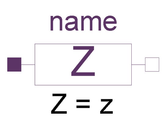
Figure 12.
Toolkit icon for a series impedance element.
In Figure 12, name refers to the annotation (name of the object of class Impedance) for the model when included in a simulation. Values for the base impedance are set by the variable z by clicking on the icon.
As an example of a two-port device model created in the toolkit, Figure 13 shows the graphics layer of an AC/DC converter, where the left side of the component is the “input” port, consisting of AC harmonic voltages and currents. The input port is modeled in the form of an extended loadBase class, which itself is extended from the twoPinBase one-port base class described above. The right side of the component in Figure 13 is the “output” port, representing the DC side of the converter. The DC side is a controlled DC voltage source, which can be connected to other DC devices in the network.
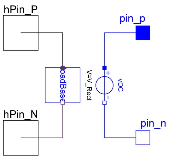
Figure 13.
Two-port converter device model underlying interconnects.
The Modelica code below shows a partial listing of the underlying component objects in the AC/DC converter model. Relations defining the harmonic power flow, corresponding to the device model described in Section 3.5.3, are defined in the equation section. (see the toolkit source code for the complete script).
- 1
- model ACDC_converter “AC to DC converter”
- 2
- outer HPF.SystemDef systemDef;
- 3
- import Modelica.ComplexMath.j;
- 4
- Modelica.Electrical.Analog.Interfaces.PositivePin pin_p;
- 5
- Modelica.Electrical.Analog.Interfaces.NegativePin pin_n;
- 6
- HPF.SinglePhase.Interface.HPin_P hPin_P(h = systemDef.numHrm);
- 7
- HPF.SinglePhase.Interface.HPin_N hPin_N(h = systemDef.numHrm);
- 8
- Modelica.Electrical.Analog.Sources.ConstantVoltage vDC(V = V_Rect);
- 9
- HPF.SinglePhase.Interface.LoadBase loadBase;
- 10
- …
- 11
- equation
- 12
- …
- 13
- end ACDC_converter
4.5. System Solver
As a physical systems modeling language, Modelica insulates the user from the underlying solver implementation, allowing the user to focus only on modeling system behavior. Solving the system of equations—as described by the language—is offloaded to the underlying Modelica compiler.
Every variable in Modelica is time-stamped by default. For a linear system comprising a set of ordinary differential equations, Modelica solves the system using numerical integration. However, harmonic power flow is a nonlinear algebraic problem and therefore requires an iterative nonlinear solver. Given a defined nonlinear algebraic system, the Modelica compiler chooses from among its installed iterative root-finding algorithms to solve the system. The Newton–Raphson solver, a popular nonlinear solver, is installed by default in Dymola and OpenModelica.
In the work described here, the library was used to compute steady-state solutions for voltages and currents needed for estimation of steady-state device and system efficiencies. However, because Modelica is inherently time-based, the toolkit can be called sequentially to simulate quasi-static, time-varying loading conditions (i.e., a series of steady-state solutions which neglect transient effects), such as hourly load variations in a building over a 24 h time period.
Simulation Example
A graphical representation of a complete electrical network using BEEAM library components is shown in Figure 14; this circuit corresponds to the electrical configuration of Scenario 2.3 in Section 5. System simulation parameters are defined in a top-level block (upper left in Figure 14) called “System Setup” that assigns variables within the SystemDef class. For this example, the system parameters were set to: hrms = (harmonics to be simulated); fFund = Hz (fundamental frequency); fSamp = Hz (sampling frequency when visualizing time-domain waveforms). Parameters for devices, such as the voltage source, transformer, and other components, are set using pop-up windows for each device. The simulation output for this circuit is described in Section 5.
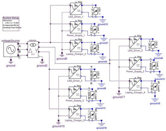
Figure 14.
Graphical representation of example electrical network in BEEAM, corresponding to Scenario 2.3 in Section 5.
5. Toolkit Validation
To evaluate the accuracy of the software developed in this work, simulations using the toolkit were compared to laboratory measurements on an experimental testbed constructed at the Powerhouse Energy Campus at Colorado State University. The following sections describe the laboratory experiments and comparison to simulations using BEEAM.
5.1. Laboratory Experiments
The experimental testbed was designed to emulate realistic loads found in a small office building, comprising laptop computer chargers, LED lighting systems, and miscellaneous DC and AC loads. The testbed also enabled both AC and DC configurations, under either balanced or unbalanced loading.
A notional diagram of the testbed is shown in Figure 15, where Figure 15a represents the AC and Figure 15b the DC distribution configuration. The testbed comprised a three-phase -Y building transformer with three parallel load branches in both configurations; loads were connected to a single phase or multiple phases. The primary side of the transformer, connected in , was tied to utility mains. Each load branch in the AC distribution case consisted of a parallel combination of one or more of the following devices: a laptop AC/DC power supply with a controllable load bank (CLB), light emitting diode (LED), light fixture supplied by an AC/DC driver, AC/DC power supplies with resistive loads, and resistive heating elements. In the DC configuration, the output voltage of the building transformer (the same used in the AC case) was converted to DC voltage with an AC/DC “central converter”. Each DC load branch consisted of one or more of the following devices: laptop DC/DC power supply connected to a CLB, light emitting diode (LED) light fixture, and fixed resistive loads.
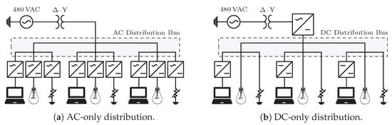
Figure 15.
Testbed configurations with AC-only (a) and DC-only (b).
The physical testbed is shown in Figure 16. The testbed was constructed using industrial-grade electrical equipment, mounted on a panel-board for convenience during configuration changes and access to measurement points. To implement configuration changes and provide circuit protection, an electrical enclosure (“load center”) contained switches and fuses, supplying a total of six possible load branches.
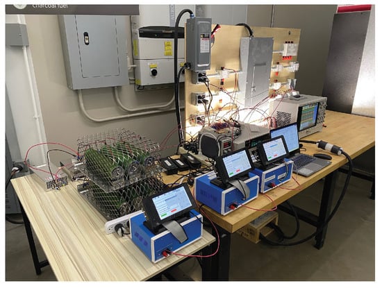
Figure 16.
Testbed hardware with power analyzer, laptop, LEDs and resistive load banks. (Photo used with permission by Arthur Santos of Colorado State University.)
The load center was connected to utility mains through a 3 kVA, -Y transformer (ACME, model T2A533081S), with 480 V primary and 208 V/120 V secondary. Power devices in the testbed consisted of: Power Supply 1 (Mean Well, RSP-1000-48), Power Supply 2 (Xunbuma, T-1000-48V), Power Supply 3 (Mean Well, SE-1000-48), Central Converter (Nextek, PHD16-ACDC-DIM-P-24-6), Laptop Charger 1 (HP, 391174-001), Laptop Charger 2 (HP, PA-1900-15C2), Laptop Charger 3 (HP, PA-1121-12H), Laptop Chargers 4–6 (Bix Power, BX-DD90X-24V), LED Drivers 1–3 (Mean Well, APV-25-24), LEDs 1–3 (24 VDC, 22 W, 2500 lumens), 200 kW (Lasko), 400–900 kW (unbranded) heating elements, and three 400 W and 20 V (custom-built) resistive CLBs.
Using six different wiring configurations and for loading conditions, a set of 24 experimental scenarios were implemented and measured. Herein, each scenario is referred to by wiring configuration and load condition as “Scenario ”, where is the winding configuration number and is the loading condition. When referring collectively to all loading conditions under a given winding configuration, the shorthand “Scenario w” is used. The AC configurations were used to obtain experimental measurements in 16 scenarios (Scenarios 1.1–1.4, 2.1–2.4, 3.1–3.4, 4.1–4.4); the DC configuration was used for obtaining measurements under eight scenarios (Scenarios 5.1–5.4, 6.1–6.4).
In Scenarios 1 and 2, power electronic loads on the secondary side of the transformer were connected as shown in Table 1. In these scenarios, the four loading values were applied to the converters as follows. The AC/DC power supplies were operated under loads of: no load, , , or . The laptop chargers were connected to the controllable load banks, set to power levels specified below. The LED drivers were loaded with LEDs 1–3 or no load. Data was collected using a Keysight multifunction switch measuring unit (MU) model 34980A with Keysight 34921T multiplexer and a Keysight PA2203A power analyzer.

Table 1.
Device configurations for AC Scenarios 1 and 2.
Scenarios 3 and 4 were the same as Scenarios 1 and 2, except that the AC/DC power supplies and resistances were replaced by heaters drawing approximately the same rated power level. The converter connections under these scenarios are shown in Table 2. Loads applied to the converters with respect to each phase in Scenarios 1–4 are shown in Table 3.
Table 2.
Device configurations for AC Scenarios 3 and 4.
Table 3.
Load power settings for AC Scenarios 1–4.
In the DC configuration for Scenarios 5 and 6, DC voltage was supplied by the central AC/DC converter, and the load converters consisted of: DC/DC laptop chargers; CLB 1–3, which were connected to DC/DC laptop chargers 4–6, respectively; LEDs; and resistors. Scenario 5 was identical to Scenario 6, except that in Scenario 5, the central converter was supplied with 120 V on the AC side, and in Scenario 6 it was supplied with 208 V. The four load power levels for each DC scenario are shown in Table 4.
Table 4.
Load power settings for DC Scenarios 5 and 6.
5.2. Comparison of Toolkit Results with Measurements
To evaluate the accuracy of predicted electrical efficiency using the toolkit, simulations of the experimental scenarios described above were performed using the BEEAM toolkit and compared to experimental measurements. Predicted total system efficiencies accumulated over all devices in the network are compared to measured system efficiencies for Scenarios 1 and 2, 3 and 4, and 5 and 6 in Figure 17, Figure 18 and Figure 19, respectively. As shown in Figure 17, Figure 18 and Figure 19, total system efficiency predicted by the toolkit matched well with measured efficiencies over all scenarios. Predicted total system power losses in the network in Scenarios 1 and 2, 3 and 4, and 5 and 6 are shown in Figure 20, Figure 21 and Figure 22, respectively. Again, simulated total power losses show reasonably good agreement with the experimental measurements in all scenarios. Additionally, shown in Figure 17, Figure 18, Figure 19, Figure 20, Figure 21 and Figure 22 are error bars on measured quantities; a detailed analysis of measurement uncertainty is given in the Appendix A.
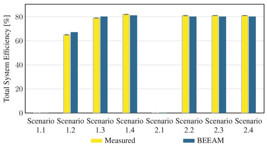
Figure 17.
Predicted versus measured total system efficiencies, Scenarios 1 and 2.
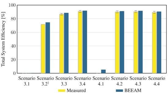
Figure 18.
Predicted versus measured total system efficiencies, Scenarios 3 and 4. indicates that uncertainty could not be estimated; see Appendix A.4.
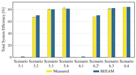
Figure 19.
Predicted versus measured total system efficiencies, Scenarios 5 and 6. indicates that uncertainty could not be estimated; see Appendix A.4.
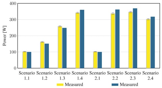
Figure 20.
Predicted versus measured total system power losses, Scenarios 1 and 2.
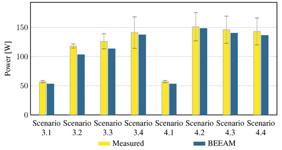
Figure 21.
Predicted versus measured total system power losses, Scenarios 3 and 4.
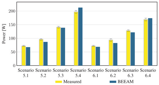
Figure 22.
Predicted versus measured total system power losses, Scenarios 5 and 6.
Discussion: Comparison of predicted versus measured efficiencies and power losses in the initial toolkit implementation revealed that system- and device-level efficiencies could be predicted with reasonable accuracy in AC and DC configurations in both balanced and unbalanced conditions. The maximum estimated error for system efficiency throughout all scenarios was 3%. Measured and modeled system efficiency agreed within the experimental uncertainty in approximately half the scenarios (see Appendix A). However, on an absolute wattage loss basis, further improvements to the underlying component models were identified.
Discrepancies between simulated and measured power values were likely attributable to simplifying assumptions made in the initial implementation of the toolkit. One simplification was in the building transformer model used in the validation studies. In particular, the balanced and linear three-phase transformer modeling approach depicted in Figure 8 was used for simplicity. This model assumes the secondary load is balanced, and consequently neglects potential coupling between phase currents and their harmonics. Second, it was assumed that the transformer was linear, with parameters extracted from measurements taken under purely sinusoidal, non-magnetically saturated conditions. In future work, the transformer model will be improved by accounting for load imbalance and phase coupling using a symmetrical components model.
Note that although the loads used in this small-scale validation study are representative of a typical small office, the load levels and the AC and DC distribution system components are not necessarily representative of a real building’s operation. The purpose of the validation experiments was to validate the modeling toolkit, not to establish whether AC or DC distribution is more efficient in the general case. Therefore, the experimental results shown in the foregoing should not be considered as predictive of real-world efficiency for AC or DC distribution systems.
6. Conclusions
In this paper, a one- and two-port network framework and open source software toolkit for comparing electrical efficiencies in AC, DC, and hybrid AC/DC distribution systems for buildings was described. The new software toolkit, BEEAM, accounts for harmonics in currents or voltages in the distribution system by specifying nonlinear device-specific functional relations between voltage and current harmonics for all nonlinear devices in the system. The solution for the voltage and current phasors at each harmonic in the network is obtained using a harmonic power flow approach, from which device- and system-level power losses and efficiencies are computed. The BEEAM toolkit was implemented in Modelica, complete with a component library, graphical interface, user guide, and examples [27].
Comparison of predicted versus measured efficiencies and power losses in the initial toolkit implementation revealed that device- and system-level efficiencies could be predicted with reasonably good accuracy under both balanced and unbalanced AC scenarios in a small-scale laboratory validation experiment. A detailed uncertainty analysis also demonstrated that the maximum estimated error for system efficiency across all scenarios was 3% and that the measured and modeled system efficiency agreed within the experimental uncertainty in approximately half the scenarios.
Some limitations to this work were: (a) the initial validation studies shown herein were performed on a small-scale demonstration testbed that did not include some devices that could be found in modern buildings, e.g., renewable generators and three-phase converters; (b) a balanced, linear transformer model was used in the validation studies that neglected potential coupling and harmonics between electrical phases in the transformer or any nonlinearities; (c) device-specific behavioral functions in the initial toolkit were represented using interpolation using experimental device measurements; and (d) investigation into the relative contributions of harmonics from active and reactive power and how they impact the efficiency calculations.
Future work (currently underway) will further develop and validate BEEAM in new test configurations, to include co-simulation of electrical and thermal building system performance in bench-scale and full-scale laboratory demonstrations and the analysis of harmonic contributions from active and reactive power flows. The toolkit transformer model will also be improved to allow the removal of the assumption of a balanced, linear transformer by using a full representation symmetrical components. Finally, additional research is underway to establish closed-form parametric models for the device-specific behavioral functions for a class of power-electronic devices, along with a numerical fitting procedure to extract the best-fit parameters. These closed-form models are expected to improve the computational efficiency of BEEAM, by avoiding interpolation steps. Beyond these activities, recommended future work to extend this research is the development and validation of three-phase converter models compatible with BEEAM and suitable for larger buildings studies.
Author Contributions
Conceptualization, J.C., S.F. and O.G.; Methodology, A.O. and J.C.; Software, A.O.; Validation, A.S. and D.Z.; Formal analysis, A.O. and S.F.; Resources, D.Z.; Data curation, A.S., G.D. and D.G.; Writing–original draft, A.O., J.C., A.S. and S.F.; Project administration, S.F.; Funding acquisition, S.F. All authors have read and agreed to the published version of the manuscript.
Funding
This work was authored in part by the National Renewable Energy Laboratory, operated by the Alliance for Sustainable Energy, LLC, for the U.S. Department of Energy (DOE) under Contract No. DE-AC36-08-GO28308; and by Lawrence Berkeley National Laboratory, operated for the DOE under Contract No. DE-AC02-05CH11231. Funding was provided by the DOE Assistant Secretary for Energy Efficiency and Renewable Energy Building Technologies Office Emerging Technologies Program. The views expressed in this article do not necessarily represent the views of the DOE or U.S. Government.
Data Availability Statement
Experimental measurements described in Section 5 of this paper and calculations for the uncertainty analysis in Appendix A are contained in the publicly-available dataset located at https://doi.org/10.5061/dryad.m63xsj471. In addition, the BEEAM software toolkit is available at https://github.com/NREL/BEEAM.
Conflicts of Interest
The authors declare no conflict of interest.
Nomenclature
| Indices and Sets | |
| Set of harmonic numbers | |
| Set of one-port networks in electrical model | |
| Set of two-port networks in electrical model | |
| Set of all devices in the model, | |
| Set of subgraphs formed by ideal interconnects between network ports | |
| Set of device port numbers | |
| Number of edges (branches) in subgraph g | |
| Number of nodes in subgraph g | |
| E | Total number of edges (branches) across all subgraphs, |
| N | Total number of nodes across all subgraphs, |
| Variables | |
| Current phasor into port p of device d at harmonic h | |
| Voltage phasor at port p of device d at harmonic h | |
| Average real input power, into device d, port p | |
| Average real output power, out of device d at port p | |
| Average power loss, in device d | |
| Functions and Parameters | |
| Loss function for device d | |
| Device specific behavioral function for device d | |
| Vector of behavioral parameters for device d | |
| Vector of one-stage loss parameters for device d | |
| Vector of two-stage loss parameters for device d |
Appendix A. Uncertainty Estimation
This appendix describes the uncertainty analysis methodology used for the experimental validation of the BEEAM library, corresponding to the validation experiments described in Section 5.
Appendix A.1. Data Collection
As described in Section 5, the validation experiment included 24 scenarios (16 with an AC distribution and 8 with a DC distribution). Each scenario was repeated three times; the measured values reported represent the averages of the three runs.
Appendix A.1.1. Instrumentation
Instrumentation used in the experiment consisted of two Keysight PA2203A power analyzers, one Keysight 34980A multifunction switch, six LEM LTS 6-NP current transducers, and six Belkin Wemo F7C029 Insight smart plugs. Table A1 summarizes the accuracy specifications for these instruments.
Table A1.
Instrument accuracy specifications.
Table A1.
Instrument accuracy specifications.
| Instrument | Rated Accuracy |
|---|---|
| Keysight PA2203A Power Analyzer | |
| Keysight 34980A Multifunction Switch with 34921T Multiplexer | ; range-dependent |
| LEM LTS 6-NP Current Transducer | |
| Belkin Wemo F7C029 Insight Smart Plug | Not specified; estimated at |
Appendix A.1.2. Keysight PA2203A Power Analyzer
All channels of the Keysight PA2203A power analyzer were configured with a 1:1 voltage probe and internal 50A current measurement for all scenarios. In this configuration, the power analyzer’s specified accuracy [36] was
in which the power range is the multiple of the voltage and current ranges and
where for the voltage probes used. For each scenario, the voltage and current range selected by the power analyzer for each channel were recorded and used to calculate the channel’s power range.
Appendix A.1.3. Keysight 34980A Multifunction Switch
The Keysight 34980A multifunction switch with a 34921T multiplexer module installed was used to measure DC voltages. The unit’s specified accuracy [37] was:
- for the 10 V range
- for the 100 V range.
As the unit was set to the “auto-range” function during all experimental runs, we used the 10 V range to measure the output of the LTS 6-NP current transducers and the 100 V range to measure all other voltages.
Appendix A.1.4. LEM LTS 6-NP Current Transducer
The LEM LTS 6-NP DC current transducer has a specified accuracy of , in which the nominal primary current (full scale) () is [38]. The transducer output voltage was
in which the polarity of the second term depends on the polarity of measured current, . As the experiments were performed in a temperature-controlled laboratory; temperature drift for ambient conditions was assumed to be negligible.
Appendix A.1.5. Belkin Wemo Smart Plug
The Belkin Wemo F7C029 Insight smart plug provided pass-through measurement of 120 VAC receptacle loads. (The F7C029 is an older model which is now out of production; however, Belkin technical support provides a “Frequently Asked Questions” webpage [39].) This device does not have a manufacturer-specified accuracy. The authors tested the accuracy of multiple Wemo smart plugs while measuring 200 and 400 W loads using a PA2203A power analyzer as a reference. Approximately 92% of Wemo smart plug samples were within of the power analyzer reference, and 100% of samples were within . Therefore, our analysis used as the Wemo smart plug accuracy specification.
Appendix A.1.6. System Topology
Figure A1, Figure A2, Figure A3, Figure A4, Figure A5, Figure A6 and Figure A7 display electrical diagrams for all scenarios with connected instrumentation. In Scenarios 3 and 4, heaters and their associated smart plugs were included in the circuit only if active for the loading condition. For Scenarios 5 and 6, loading conditions included one load resistor, included four load resistors, and included all seven load resistors. Each load resistor in Scenarios 5 and 6 was nominally 85 W at 24 VDC.

Figure A1.
Electrical diagrams for Scenarios 1 and 2. (a) Electrical diagrams for Scenarios 1.1 and 2.1. (b) Electrical diagrams for Scenarios 1.2–4 and 2.2–4.
Figure A1.
Electrical diagrams for Scenarios 1 and 2. (a) Electrical diagrams for Scenarios 1.1 and 2.1. (b) Electrical diagrams for Scenarios 1.2–4 and 2.2–4.


Figure A2.
Electrical diagrams for Scenarios 3.1-2 and 4.1. (a) Electrical diagrams for Scenarios 3.1 and 4.1. (b) Electrical diagrams for Scenario 3.2.
Figure A2.
Electrical diagrams for Scenarios 3.1-2 and 4.1. (a) Electrical diagrams for Scenarios 3.1 and 4.1. (b) Electrical diagrams for Scenario 3.2.


Figure A3.
Electrical diagrams for Scenarios 3.3, 3.4, 4.2–4, 5.1, and 6.1.
Figure A3.
Electrical diagrams for Scenarios 3.3, 3.4, 4.2–4, 5.1, and 6.1.


Figure A4.
Electrical diagrams for Scenarios 5.1 and 6.1.
Figure A4.
Electrical diagrams for Scenarios 5.1 and 6.1.


Figure A5.
Electrical diagrams for Scenarios 5.2 and 6.2.
Figure A5.
Electrical diagrams for Scenarios 5.2 and 6.2.


Figure A6.
Electrical diagrams for Scenarios 5.3 and 6.3.
Figure A6.
Electrical diagrams for Scenarios 5.3 and 6.3.


Figure A7.
Electrical diagrams for Scenarios 5.4 and 6.4.
Figure A7.
Electrical diagrams for Scenarios 5.4 and 6.4.

Appendix A.2. Uncertainty Calculations
The uncertainty analysis combines the uncertainty associated with random (Type A) errors and systematic (Type B) errors, per their NIST definitions [40]. For each quantify of interest, Type A uncertainty equals the estimated standard deviation from the three runs conducted for each scenario, and Type B uncertainty was calculated from the instruments’ rated accuracies. Uncertainty estimates were combined using the standard rules for error propagation [40,41]. Total uncertainties are reported using a 95% confidence interval (). An excel spreadsheet that implements all the uncertainty calculations is provided with this appendix.
Appendix A.2.1. Notation
Throughout the following sections, refers to the estimated standard deviation of quantity x; represents the Type A component of uncertainty, that is, the estimated standard deviation of the experimental measurements; , , , and represent the Type B components of uncertainty associated with the power analyzer, digital multimeter (multiplexer), current transducer, and smart plug, respectively; and i is a generic index associated with sets of multiple devices of the same type. To avoid a proliferation of indices, uncertainty components s are always defined locally to the quantity x being discussed.
Appendix A.2.2. Assumptions
The following assumptions were used throughout the uncertainty analysis:
- Measurements made for the same scenario with the same instrument have systematic (Type B) error characterized by the instruments’ rated accuracy.
- As the manufacturers data sheets did not specify the coverage (prediction interval) associated with the rated accuracy, the rated accuracy for all instruments was assumed to correspond to 99.7% coverage (). Therefore, for each instrument k, .
- Errors attributable to Type A and Type B uncertainty were uncorrelated.
- Wemo smart plug measurements include the smart plugs’ known self-consumption of approximately 1.5 W.
Appendix A.2.3. System Input
The system input power was measured at the transformer primary with the power analyzer configured for three-phase, power measurement. In this configuration, the power analyzer reports individual Y-transformed measured power values , , and . For each phase , the estimated standard deviation is
in which is one-third of the accuracy range calculated according to (A1) based on the voltage and current ranges used for the scenario. Given the relationship
the individual phase standard deviation estimates are combined as follows:
Appendix A.2.4. Transformer Secondary
For Scenarios 1–4, the transformer secondary power was measured using the power analyzer configured for three-phase, Y power measurement. Estimates of the phase standard deviations , , and were calculated according to (A4) and combined as:
In Scenarios 5 and 6, only the Nextek PHD was connected to the transformer secondary. Therefore, a single-channel, single-phase power measurement of the Nextek input was made: for Scenario 5, with the voltage probe connected line-neutral; and for Scenario 6, with the voltage probe connected line–line. and were calculated according to (A4), for Scenario 5 and for Scenario 6.
Appendix A.2.5. System Output
The system output power is the sum of the measured or calculated output power for each load device i present in the scenario,
The estimated standard deviation was therefore
Derivations for the individual standard deviations follow.
Appendix A.2.6. DC Load
Output power for DC load resistors and load banks was calculated using either or , depending on the measurements available. In all cases, DC voltage was measured using the multifunction switch as a digital multimeter (DMM). The voltage uncertainty is given by
in which is one-third of the accuracy range calculated according to the formula provided in Appendix A.1.3 for the 100 V range.
DC load current was measured using the LTS 6-NP current transducers; the transducer output was then read using the DMM. The DDM voltage is given by (A3). Therefore, the uncertainty in the current reading attributable to the DMM is
in which is one-third of the accuracy range calculated according to the formula provided in Appendix A.1.3 for the 10 V range. The uncertainty attributable to the transducer is one-third of 0.7% of 6 A, or . The combined estimate of standard deviation is
For some scenarios, not all DC load currents could be measured, given the equipment available. Instead, the DC load resistances were independently characterized under load using the power analyzer. The Type A uncertainty of the resistance was obtained by estimating the standard deviation of the resistance values measured during the characterization test. (Type B uncertainty was not computed for the resistances.) The average resistances and their associated standard deviations were used directly in the uncertainty analysis.
For the case, the covariance between voltage and current was obtained from the experimental measurements. The overall power uncertainty was
For the case, the resistance and voltage values were assumed to be independent (no covariance). The overall power uncertainty was therefore
Appendix A.2.7. LED Lighting Load
In Scenarios 1–4, the LED lighting load voltage and current were measured with the DMM. Therefore, the uncertainty is given by (A14). However, in Scenarios 5 and 6, LED load power was measured directly using the power analyzer (one channel per LED). For Scenarios 5 and 6 only,
in which is one-third of the accuracy range calculated according to (A1) based on the voltage and current ranges used to measure LED i.
Appendix A.2.8. Heater Load
Space heater power in Scenarios 3 and 4 was measured using the Wemo smart plus, for which the accuracy was estimated at ; that is, . The combined uncertainty was
Appendix A.3. System Losses
Independent estimates with uncertainties were obtained for transformer loss, converter loss, and total system loss.
Appendix A.3.1. Transformer Loss
For each scenario, the transformer loss was
The associated uncertainty was
Appendix A.3.2. Converter Loss
The converter loss was
The associated uncertainty was
Appendix A.3.3. Total System Loss
The total system loss was
The associated uncertainty was
Appendix A.4. Efficiency
For each scenario, the calculated system efficiency was
The associated uncertainty was
in which is the covariance in the values of and observed in the measured data. In Scenarios 3.2 and 6.2, the estimate obtained for was a large negative value that rendered the argument of the square root function in (A25) negative; this prevented the team from obtaining uncertainty estimates for in these two scenarios.
Appendix A.5. Results
For all scenarios, the average values of the measured device power values were used as the input to the associated power flow model. Modeled values for input power , transformer secondary power , transformer loss , converter loss , total system loss , and system efficiency were extracted from the simulation results. Table A2, Table A3 and Table A4 compare the measured and modeled values of these quantities.
Table A2.
Measured and modeled values for system input power and transformer secondary power.
Table A2.
Measured and modeled values for system input power and transformer secondary power.
| System Input Power | Transformer Secondary Power | |||
|---|---|---|---|---|
| Scenario | Measured | Modeled | Measured | Modeled |
| 1.1 | W | W | W | W |
| 1.2 | W | W | W | W |
| 1.3 | W | W | W | W |
| 1.4 | W | W | W | W |
| 2.1 | W | W | W | W |
| 2.2 | W | W | W | W |
| 2.3 | W | W | W | W |
| 2.4 | W | W | W | W |
| 3.1 | W | W | W | W |
| 3.2 | W | W | W | W |
| 3.3 | W | W | W | W |
| 3.4 | W | W | W | W |
| 4.1 | W | W | W | W |
| 4.2 | W | W | W | W |
| 4.3 | W | W | W | W |
| 4.4 | W | W | W | W |
| 5.1 | W | W | W | W |
| 5.2 | W | W | W | W |
| 5.3 | W | W | W | W |
| 5.4 | W | W | W | W |
| 6.1 | W | W | W | W |
| 6.2 | W | W | W | W |
| 6.3 | W | W | W | W |
| 6.4 | W | W | W | W |
Table A3.
Measured and modeled values for transformer and converter losses.
Table A3.
Measured and modeled values for transformer and converter losses.
| Transformer Loss | Converter Loss | |||
|---|---|---|---|---|
| Scenario | Measured | Modeled | Measured | Modeled |
| 1.1 | W | W | W | W |
| 1.2 | W | W | W | W |
| 1.3 | W | W | W | W |
| 1.4 | W | W | W | W |
| 2.1 | W | W | W | W |
| 2.2 | W | W | W | W |
| 2.3 | W | W | W | W |
| 2.4 | W | W | W | W |
| 3.1 | W | W | W | W |
| 3.2 | W | W | W | W |
| 3.3 | W | W | W | W |
| 3.4 | W | W | W | W |
| 4.1 | W | W | W | W |
| 4.2 | W | W | W | W |
| 4.3 | W | W | W | W |
| 4.4 | W | W | W | W |
| 5.1 | W | W | W | W |
| 5.2 | W | W | W | W |
| 5.3 | W | W | W | W |
| 5.4 | W | W | W | W |
| 6.1 | W | W | W | W |
| 6.2 | W | W | W | W |
| 6.3 | W | W | W | W |
| 6.4 | W | W | W | W |
Table A4.
Measured and modeled values for total system loss and efficiency.
Table A4.
Measured and modeled values for total system loss and efficiency.
| Total System Loss | Efficiency | |||
|---|---|---|---|---|
| Scenario | Measured | Modeled | Measured | Modeled |
| 1.1 | W | W | – | – |
| 1.2 | W | W | % | % |
| 1.3 | W | W | % | % |
| 1.4 | W | W | % | % |
| 2.1 | W | W | – | – |
| 2.2 | W | W | % | % |
| 2.3 | W | W | % | % |
| 2.4 | W | W | % | % |
| 3.1 | W | W | – | – |
| 3.2 | W | W | % † | % |
| 3.3 | W | W | % | % |
| 3.4 | W | W | % | % |
| 4.1 | W | W | – | – |
| 4.2 | W | W | % | % |
| 4.3 | W | W | % | % |
| 4.4 | W | W | % | % |
| 5.1 | W | W | – | – |
| 5.2 | W | W | % | % |
| 5.3 | W | W | % | % |
| 5.4 | W | W | % | % |
| 6.1 | W | W | – | – |
| 6.2 | W | W | % † | % |
| 6.3 | W | W | % | % |
| 6.4 | W | W | % | % |
† Uncertainty value could not be calculated due to large estimate of covariance; see Appendix A.4.
Figure A8, Figure A9, Figure A10, Figure A11, Figure A12, Figure A13, Figure A14, Figure A15, Figure A16, Figure A17, Figure A18 and Figure A19 compare the measured and modeled system input power and total system loss for all scenarios. These figures supplement Figure 17, Figure 18, Figure 19, Figure 20, Figure 21 and Figure 22 in Section 5.

Figure A8.
Predicted versus measured total system input power, Scenarios 1 and 2.
Figure A8.
Predicted versus measured total system input power, Scenarios 1 and 2.


Figure A9.
Predicted versus measured total system input power, Scenarios 3 and 4.
Figure A9.
Predicted versus measured total system input power, Scenarios 3 and 4.


Figure A10.
Predicted versus measured total system input power, Scenarios 5 and 6.
Figure A10.
Predicted versus measured total system input power, Scenarios 5 and 6.


Figure A11.
Predicted versus measured transformer power, secondary; Scenarios 1 and 2.
Figure A11.
Predicted versus measured transformer power, secondary; Scenarios 1 and 2.


Figure A12.
Predicted versus measured transformer power, secondary; Scenarios 3 and 4.
Figure A12.
Predicted versus measured transformer power, secondary; Scenarios 3 and 4.


Figure A13.
Predicted versus measured transformer power, secondary; Scenarios 5 and 6.
Figure A13.
Predicted versus measured transformer power, secondary; Scenarios 5 and 6.


Figure A14.
Predicted versus measured transformer loss, Scenarios 1 and 2.
Figure A14.
Predicted versus measured transformer loss, Scenarios 1 and 2.


Figure A15.
Predicted versus measured transformer loss, Scenarios 3 and 4.
Figure A15.
Predicted versus measured transformer loss, Scenarios 3 and 4.


Figure A16.
Predicted versus measured transformer loss, Scenarios 5 and 6.
Figure A16.
Predicted versus measured transformer loss, Scenarios 5 and 6.


Figure A17.
Predicted versus measured converter loss, Scenarios 1 and 2.
Figure A17.
Predicted versus measured converter loss, Scenarios 1 and 2.


Figure A18.
Predicted versus measured converter loss, Scenarios 3 and 4.
Figure A18.
Predicted versus measured converter loss, Scenarios 3 and 4.


Figure A19.
Predicted versus measured converter loss, Scenarios 5 and 6.
Figure A19.
Predicted versus measured converter loss, Scenarios 5 and 6.

References
- Hendron, R.; Eastment, M. Development of an Energy-Savings Calculation Methodology for Residential Miscellaneous Electric Loads; Technical Report; National Renewable Energy Lab. (NREL): Golden, CO, USA, 2006.
- Comstock, O.; Jarzomski, K. Consumption and saturation trends of residential miscellaneous end-use loads. In Proceedings of the 2012 ACEEE Summer Study Energy Efficiency Buildings, Pacific Grove, CA, USA, 12–17 August 2012; Volume 14. [Google Scholar]
- George, K. DC Power Production, Delivery and Utilization; White Paper; Electric Power Research Institute: Palo Alto, CA, USA, 2006. [Google Scholar]
- Boroyevich, D.; Cvetković, I.; Dong, D.; Burgos, R.; Wang, F.; Lee, F. Future Electronic Power Distribution Systems a Contemplative View. In Proceedings of the 2010 12th International Conference on Optimization of Electrical and Electronic Equipment, Brasov, Romania, 20–22 May 2010; pp. 1369–1380. [Google Scholar] [CrossRef]
- Savage, P.; Nordhaus, R.R.; Jamieson, S.P. DC Microgrids: Benefits and Barriers; Technical Report; Yale University, REIL, Yale School of Forestry & Environmental Studies: New Haven, CT, USA, 2010. [Google Scholar]
- Vossos, V.; Garbesi, K.; Shen, H. Energy savings from direct-DC in U.S. residential buildings. Energy Build. 2014, 68, 223–231. [Google Scholar] [CrossRef]
- Mackay, L.; van der Blij, N.H.; Ramirez-Elizondo, L.; Bauer, P. Toward the Universal DC Distribution System. Electr. Power Components Syst. 2017, 45, 1032–1042. [Google Scholar] [CrossRef]
- Prabhala, V.A.; Baddipadiga, B.P.; Fajri, P.; Ferdowsi, M. An Overview of Direct Current Distribution System Architectures & Benefits. Energies 2018, 11, 2463. [Google Scholar] [CrossRef]
- Gerber, D.L.; Vossos, V.; Feng, W.; Marnay, C.; Nordman, B.; Brown, R. A simulation-based efficiency comparison of AC and DC power distribution networks in commercial buildings. Appl. Energy 2018, 210, 1167–1187. [Google Scholar] [CrossRef]
- Belu, R. Building Electrical Systems and Distribution Networks: An Introduction; CRC Press: Boca Raton, FL, USA, 2020. [Google Scholar]
- Hadjsaïd, N.; Sabonnadière, J.C. Electrical Distribution Networks; John Wiley & Sons: Hoboken, NJ, USA, 2013. [Google Scholar]
- Frank, S.M.; Rebennack, S. Optimal design of mixed AC-DC distribution systems for commercial buildings: A Nonconvex Generalized Benders Decomposition approach. Eur. J. Oper. Res. 2015, 242, 710–729. [Google Scholar] [CrossRef]
- Zhang, F.; Meng, C.; Yang, Y.; Sun, C.; Ji, C.; Chen, Y.; Wei, W.; Qiu, H.; Yang, G. Advantages and challenges of DC microgrid for commercial building a case study from Xiamen university DC microgrid. In Proceedings of the 2015 IEEE First International Conference on DC Microgrids (ICDCM), Atlanta, GA, USA, 7–10 June 2015; pp. 355–358. [Google Scholar] [CrossRef]
- Vossos, V.; Gerber, D.; Bennani, Y.; Brown, R.; Marnay, C. Techno-Economic Analysis of DC Power Distribution in Commercial Buildings. Appl. Energy 2018, 230, 663–678. [Google Scholar] [CrossRef]
- Wu, Y.; Wang, Z.; Huangfu, Y.; Ravey, A.; Chrenko, D.; Gao, F. Hierarchical Operation of Electric Vehicle Charging Station in Smart Grid Integration Applications—An Overview. Int. J. Electr. Power Energy Syst. 2022, 139, 108005. [Google Scholar] [CrossRef]
- Shenai, K.; Shah, K. Smart DC micro-grid for efficient utilization of distributed renewable energy. In Proceedings of the IEEE 2011 EnergyTech, Cleveland, OH, USA, 25–26 May 2011; pp. 1–6. [Google Scholar] [CrossRef]
- AlLee, G.; Tschudi, W. Edison Redux: 380 Vdc Brings Reliability and Efficiency to Sustainable Data Centers. IEEE Power Energy Mag. 2012, 10, 50–59. [Google Scholar] [CrossRef]
- Sannino, A.; Postiglione, G.; Bollen, M.H.J. Feasibility of a DC Network for Commercial Facilities. IEEE Trans. Ind. Appl. 2003, 39, 1499–1507. [Google Scholar] [CrossRef]
- Nilsson, D.; Sannino, A. Efficiency Analysis of Low- and Medium-Voltage DC Distribution Systems. In Proceedings of the IEEE Power Engineering Society General Meeting, Denver, CO, USA, 6–10 June 2004; 2004; Volume 2, pp. 2315–2321. [Google Scholar] [CrossRef]
- Fregosi, D.; Ravula, S.; Brhlik, D.; Saussele, J.; Frank, S.; Bonnema, E.; Scheib, J.; Wilson, E. A comparative study of DC and AC microgrids in commercial buildings across different climates and operating profiles. In Proceedings of the 2015 IEEE First International Conference on DC Microgrids (ICDCM), Atlanta, GA, USA, 7–10 June 2015; pp. 159–164. [Google Scholar] [CrossRef]
- Glasgo, B.; Azevedo, I.L.; Hendrickson, C. How much electricity can we save by using direct current circuits in homes? Understanding the potential for electricity savings and assessing feasibility of a transition towards DC powered buildings. Appl. Energy 2016, 180, 66–75. [Google Scholar] [CrossRef]
- Thomas, B.A.; Azevedo, I.L.; Morgan, G. Edison Revisited: Should we use DC circuits for lighting in commercial buildings? Energy Policy 2012, 45, 399–411. [Google Scholar] [CrossRef]
- Han, J.; Oh, Y.S.; Gwon, G.H.; Kim, D.U.; Noh, C.H.; Jung, T.H.; Lee, S.J.; Kim, C.H. Modeling and Analysis of a Low-Voltage DC Distribution System. Resources 2015, 4, 713–735. [Google Scholar] [CrossRef]
- Santos, A.; Cale, J.; Othee, A.; Gerber, D.; Frank, S.; Duggan, G.; Zimmerle, D.; Brown, R. Comparison of Load Models for Estimating Electrical Efficiency in DC Microgrids. In Proceedings of the 3rd IEEE International Conference on DC Microgrids, Matsue, Japan, 20–23 May 2019. [Google Scholar]
- Xia, D.; Heydt, G. Harmonic Power Flow Studies, Part I: Formulation and Solution. IEEE Power Eng. Rev. 1982, PER-2, 17. [Google Scholar] [CrossRef]
- Xia, G.; Heydt, G. Harmonic Power Flow Studies, Part II: Implementation and Practical Application. IEEE Trans. Power Appar. Syst. 1982, PAS-101, 1266–1270. [Google Scholar] [CrossRef]
- Building Electrical Efficiency Analysis Model (BEEAM). Available online: https://github.com/NREL/BEEAM/ (accessed on 23 February 2023).
- El-Hawary, M.E. Introduction to Electrical Power Systems; John Wiley & Sons: Hoboken, NJ, USA, 2008. [Google Scholar]
- Thomas, R.; Rosa, A. Network Topology: A Supplement to Accompany the 3rd Edition of the Analysis and Design of Linear Circuits; Wiley: New York, NY, USA, 2001. [Google Scholar]
- Cale, J.; Lute, C.; Ross, G.; Othee, A. Characterization Procedure for Unsymmetrical Split-Phase Capacitor-Start Induction Machines. IEEE Open Access J. Power Energy 2020, 8, 2–10. [Google Scholar] [CrossRef]
- King, D.; Gonzalez, G.; Galbraith, M.; Boyson, W. Performance Model for Grid-Connected Photovoltaic Inverters; Technical Report; Sandia National Laboratories: Albuquerque, NM, USA, 2007.
- Dassault Systèmes. Dymola-Dassault Systèmes®. Available online: https://www.3ds.com/products-services/catia/products/dymola/ (accessed on 24 February 2021).
- Fritzson, P.; Pop, A.; Abdelhak, K. The OpenModelica Integrated Environment for Modeling, Simulation, and Model-Based Development. Model. Identif. Control. 2020, 41, 241–295. [Google Scholar] [CrossRef]
- Franke, R.; Wiesmann, H. Flexible modeling of electrical power systems – the Modelica PowerSystems library. In Proceedings of the 10th International Modelica Conference, Lund, Sweden, 10–12 March 2014; pp. 515–522. [Google Scholar]
- Haumer, A.; Kral, C.; Gragg, J.; Kapeller, H. Quasi-Static Modeling and Simulation of Electrical Circuits using Complex Phasors. In Proceedings of the Modelica Conference 2008, University of Applied Sciences Bielefeld, Bielefeld, Germany, 3–4 March 2008. [Google Scholar]
- Keysight Technologies. IntegraVision PA2200 Series Power Analyzers. Available online: https://www.keysight.com/us/en/assets/7018-04657/data-sheets/5992-0324.pdf (accessed on 1 December 2017).
- Keysight Technologies. 34980A Data Acquisition System. Available online: https://www.lem.com/sites/default/files/products_datasheets/lts_6-np.pdf (accessed on 9 July 2019).
- LEM. Current Transducer LTS 6-NP. Available online: https://www.keysight.com/us/en/assets/7018-01247/data-sheets/5989-1437.pdf (accessed on 25 August 2017).
- Belkin International. Wemo Insight Smart Plug, F7C029 Frequently Asked Questions. Available online: https://www.belkin.com/us/support-article?articleNum=80139 (accessed on 16 March 2021).
- Taylor, B.N.; Kuyatt, C.E. Guidelines for Evaluating and Expressing the Uncertainty of NIST Measurement Results; NIST Technical Note 1297; National Institute of Standards and Technology (NIST): Gaithersburg, MD, USA, 1994.
- Bevington, P.R.; Robinson, D.K. Data Reduction and Error Analysis for the Physical Sciences, 3rd ed.; McGraw-Hill: New York, NY, USA, 2003. [Google Scholar]


Disclaimer/Publisher’s Note: The statements, opinions and data contained in all publications are solely those of the individual author(s) and contributor(s) and not of MDPI and/or the editor(s). MDPI and/or the editor(s) disclaim responsibility for any injury to people or property resulting from any ideas, methods, instructions or products referred to in the content. |
© 2023 by the authors. Licensee MDPI, Basel, Switzerland. This article is an open access article distributed under the terms and conditions of the Creative Commons Attribution (CC BY) license (https://creativecommons.org/licenses/by/4.0/).