Abstract
Solar conversion devices are generally connected with energy storage systems to overcome the influence of sunlight variability. Developing an integrated solar energy conversion and storage device is an attractive approach to compensate for the energy loss of directly connecting these separate devices. In this work, a photocapacitive device is developed based on the Cu2O/CuO heterostructure, with Cu2O as a light absorber and CuO providing a platform for electron and ion storage. The coupling of Cu2O and CuO leads to a high specific capacitance of 135 mF/cm2 under bias and an open-circuit potential of 0.62 VRHE. A photo-charge and dark-discharge ability of Cu2O/CuO system under zero-bias is also discovered and explained based on the concept of Faradaic junction. This work presents an avenue for the investigation of high-performance Cu2O-based solar energy storage devices.
1. Introduction
With the increasing energy demand of human society, the excessive consumption of fossil fuels and CO2 emission have triggered a series of environmental issues, which highlights the importance of the utilization of renewable energy resources. Solar energy is favorable due to the advantages of unlimited supply, zero pollution and low cost. Photoelectric conversion devices with high efficiencies such as solar cells have been developed in the past few decades [1,2,3,4,5]. However, solar cells are unable to fulfill the energy demand at all times, as a consequence of sunlight intermittence. Electric energy storage systems such as batteries or supercapacitors are connected to solar cells to alleviate the shortage. The direct connection of these separate devices with wires not only raises fabrication cost, but also causes power loss owing to the high external resistance and charge transferring at multiple interfaces [6].
The integration of a photoelectric conversion unit such as a solar cell or photoelectrode with a supercapacitor has therefore emerged as an attractive solution in recent years, with the advantages of a small volume, light weight and high efficiency [6,7,8]. Compared with the integration of a solar cell and supercapacitor, the coupling of a photoelectrode and supercapacitor can efficiently convert and store the solar energy as electric or chemical energy with a simpler device configuration. Different structures of integrated photocapacitive electrodes such as Cu/Cu2O, TiO2/Ni(OH)2, Fe2O3/Ni(OH)2 and BiVO4-PbOx have been investigated [9,10,11,12]. Currently, the photo-rechargeable performance of photocapacitive electrodes is still far from being commercialized. The exploration of novel photocapacitive systems is urgently needed.
Cu-based oxide and sulfide semiconducting materials have been intensively explored in the field of solar cells and photoelectrochemical water splitting [13,14,15,16,17,18,19,20]. Among these materials, Cu2O is an appealing low-cost light-absorbing material, with a suitable band gap of 2.1 eV [21,22,23,24,25]. A major issue in the solar conversion application of Cu2O semiconductors is the inherent instability of self-reduction, attributed to the fact that the redox potentials of Cu2+/Cu+ and Cu+/Cu are lying in the band gap of Cu2O. Protective layers or sacrificial agents have been applied to prevent the self-reduced reactions triggered by photo-generated electrons [23,26]. On the other hand, when utilized as photocapacitive electrodes, photo-generated carriers can be stored by the self-oxidating or reduction reaction. Different charge transfer mechanisms are involved in the application of water-splitting photocathodes and photocapacitive electrodes. In the Cu2O photocathode of hydrogen production, photo-generated hole–electron pairs are primarily separated in the heterostructure with a high photovoltage, in which electrons flow through the heterostructure to induce a water reduction reaction in the electrolyte, while holes are collected by the counter electrode [27]. In the hole-storage Cu2O photocapacitive electrode, hole–electron pairs are separated in the bulk of Cu2O, in which holes are stored by the self-oxidation reaction, while electrons are collected by the counter electrode for hydrogen production [9]. A Cu/Cu2O structure photocapacitive electrode has been reported to store photogenerated holes by the oxidation reaction of Cu+/Cu2+ [9]. However, a large external bias is needed for the efficient separation of photo-generated electron-hole pairs, due to the lack of a built-in electric field in a p–n junction.
Various methods have been investigated for the fabrication of Cu2O/CuO heterostructures, such as metalorganic chemical vapor deposition (MOCVD) [28], sputtering [29], high temperature pyrolysis [30], sol–gel and thermal oxidation approaches [31]. Despite this development, it is still challenging to synthesize a Cu2O/CuO heterostructure with a good stability of bulk Cu2O and controllable CuO thickness by a facile and low-cost method. Compared to the above approaches, the electrochemical surface treatment method can be facilely carried out at room temperature and in non-vacuum conditions, in which the thickness of CuO can be mildly regulated by controlling the scan cycle and maintaining the Cu2O stability at the same time.
In this work, an integrated device for solar harvesting and electric energy storage based on the Cu2O/CuO heterostructure is firstly reported. Different from the hole-storing Cu/Cu2O heterostructure in the literature, photo-generated electrons are stored by the reduction of CuO under illumination, which are subsequently released in the dark condition. The Cu2O/CuO photocapacitive electrode shows a high specific capacitance of 135 mF/cm2 under bias and an open-circuit potential of 0.62 VRHE. Furthermore, a photo-charge and dark-discharge current density of 0.02 mA/cm2 is observed on the Cu2O/CuO heterostructure under a zero-bias condition. A possible carrier-transporting mechanism is proposed based on the concept of Faradaic junction. This work unveils the application potential of Cu2O-based heterostructures in photocapacitive devices under a low-bias condition.
2. Experimental Details
2.1. Fabrication of Cu2O Thin Films
The Cu2O thin films were prepared by an electrodeposition method according to the literature [32]. The aqueous solution for electrodeposition consisted of 0.2 M copper sulfate pentahydrate (Sinopharm, Shanghai, China), 3 M lactic acid (Sinopharm) and 0.1 M di-potassium hydrogen phosphate (Sinopharm), with a pH adjusted to 12 by adding sodium hydroxide solution. Prior to the electrodeposition process, the FTO substrates were washed with detergent, followed by sonication in deionized water and ethanol for 15 min, respectively. Electrodeposition was conducted using a three-electrode system, with FTO substrate as a working electrode, Pt foil as a counter electrode, and saturated calomel electrode (SCE) as a reference electrode. The Cu2O thin films were deposited under a current density of −1 mA/cm2 for 1600 s in a 60 ℃ solution heated with a water bath.
2.2. Electrochemical Surface Treatment of the As-Prepared Cu2O Thin Films
The Cu2O/CuO heterostructure was synthesized by an electrochemical method. The aqueous solution for surface treatment consisted of 0.5 M Na2SO4 (Sinopharm) and 0.1 M K2HPO4 (Sinopharm). The pH of the solution was adjusted to 5 by the addition of H3PO4 solution (Sinopharm). The as-prepared Cu2O thin films were subjected to voltage cycling in a potential range of −0.6 VSCE to 0.6 VSCE at a scan rate of 20 mV/s.
2.3. Materials Characterization
X-ray diffraction spectra (XRD, Bruker, Billerica, MA, USA) were measured to analyze the crystal structure. The surface and cross-sectional morphology were investigated with a scanning electron microscope (SEM, FEI). The chemical valences and surface composition were characterized with X-ray photoelectron spectroscopy (XPS, Thermo Fisher, Waltham, MA, USA). The ultraviolet visible absorption spectrum of the films was measured with a UV–visible spectrophotometer (UV-vis, Shimadzu, Kyoto, Japan).
2.4. Electrochemical and Photoelectrochemical Measurements
The electrochemical and photoelectrochemical properties were investigated with an electrochemical workstation (CHI660, Chenhua, Shanghai, China). The light source for photoelectrochemical measurement was a 500 W Xe lamp (Perfect Light). The Galvanostatic charge–discharge curves, cyclic voltammetry (CV) curves, current–time (i–t) curves and Mott–Schottky curves were measured in a three-electrode system, with Cu2O electrode, Pt foil and SCE as a working electrode, counter electrode and reference electrode, respectively. The photo-charge and dark-discharge i–t curves under zero-bias were assessed in a two-electrode system, with Cu2O electrode and Pt foil as a working electrode and counter electrode, respectively. A reversible hydrogen electrode (RHE) potential was obtained by the formula: E(V vs. RHE) = E(V vs. SCE) + 0.242 V + 0.059 × pH.
3. Results and Discussion
3.1. Characterization of Cu2O/CuO Photocapacitive Electrodes
According to the literature, Cu2O films were fabricated by an electro-deposition method [32]. As-prepared Cu2O films were subsequently treated with different CV cycles in the potential range from −0.06 VRHE to 1.14 VRHE. To evaluate the influence of voltage cycling on the morphology of Cu2O, SEM images were compared. Since the surface morphology of the Cu2O treated with 50, 100, 200 and 300 voltage cycles are similar (Figure S1), the Cu2O treated with 200 voltage cycles was chosen as a typical sample to compare with the as-prepared Cu2O in the following paragraphs. In Figure 1a, the as-prepared Cu2O shows a dense morphology with pyramidical grains exposed on the surface, similar to the typical morphology of Cu2O fabricated by the electro-deposition method in the literature [32]. The thickness of the as-prepared Cu2O is about 710 nm (Figure 1c). After 200 voltage cycles, the surface of the Cu2O is covered in wrinkled nanosheets (Figure 1b), demonstrating that chemical reactions occurred during the voltage cycles. In Figure 1d, the Cu2O treated with 200 voltage cycles shows a bilayer cross-sectional structure with a 700 nm thick dense film on the bottom and wrinkled nanosheets on the top. The results of SEM images suggest that a heterostructure was formed on the surface of Cu2O through CV cycling.
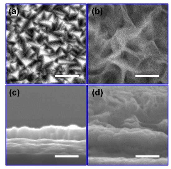
Figure 1.
Surface (a) and cross-sectional (c) SEM images of the as-prepared Cu2O photoelectrode. Surface (b) and cross-sectional (d) SEM images of the Cu2O photoelectrodes treated with 200 voltage cycles from −0.06 VRHE to 1.14 VRHE at a scan rate of 20 mV/s in a 0.5 M Na2SO4 and 0.1 M K2HPO4 aqueous solution. (The inset scale bar corresponds to 1 μm).
To analyze the phase and composition of the heterostructure, XRD and XPS spectra were measured. Figure 2a shows the XRD patterns of the as-prepared Cu2O and Cu2O treated with 50, 100, 200 and 300 voltage cycles. Except for the peaks of FTO substrate, five peaks located at 30.5°, 37.3°, 43.2°, 62.3° and 74.6° were observed in all samples, which are assigned to the (110), (111), (200), (220) and (311) planes of Cu2O (JCPDS Card No. 05-0667), respectively [24]. The peak at 37.3° shows the strongest intensity, indicating that all deposited Cu2O samples are (111)-oriented. From XRD patterns, no peak corresponding to CuO was detected in any samples, suggesting the low-crystallinity and amorphous nature of the nanosheets observed in the SEM image of Figure 1b. The peak located at 43.40o of the Cu2O treated with 300 voltage cycles was assigned to the (111) plane of Cu (JCPDS Card No. 70-3039), which is absent in the XRD patterns of the other Cu2O samples. This result indicates that part of Cu2O was reduced to Cu after 300 voltage cycles. The voltage cycling treatments were performed on four individual Cu2O samples prepared within the same parameters of an electrodeposition method. To maintain the stability of Cu2O, no heat treatment process was performed before and after the voltage cycling treatments. As a result, a variation of an amorphous background on the XRD patterns was observed, due to the fluctuation of water-bath temperature during the electrodeposition process of Cu2O.
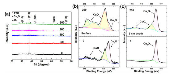
Figure 2.
(a) XRD patterns of the as-prepared Cu2O and Cu2O treated with 50, 100, 200 and 300 voltage cycles. The XPS Cu 2p region at the surface (b) and 3 nm depth bulk (c) of the as-prepared Cu2O and Cu2O treated with 200 voltage cycles.
Figure 2b,c depict the XPS Cu 2p region signal at the surface and 3 nm depth of the Cu2O samples, respectively. Figure 2b clearly demonstrates the existence of CuO on the surface of both samples. The Cu 2p peak at around 934.9 eV and the broad peak from 940 eV to 945 eV are the features of CuO. The Cu 2p peak at 932.6 eV is assigned to Cu+ [25]. The surface Cu 2p peak area ratio of Cu2+(934.9 eV)/Cu+(932.6 eV) for as-prepared Cu2O is 0.47, which increases to 5.21 after 200 voltage cycles, suggesting the oxidation of Cu2O during voltage scans. From Figure 2c, it is confirmed that Cu+ is the only existing state in the bulk of as-prepared Cu2O, while both Cu2+ and Cu+ appear in the bulk of Cu2O treated with 200 voltage cycles. To estimate the total amount of CuO formed in the voltage cycling treatment, the charge quantity of the redox reaction was calculated with the cyclic voltametric curves of the 200 voltage cycles (Figure S2). By integrating the current density with time, the total charge quantity for the redox reaction was 0.339 C, corresponding to the formation of 3.51 μmol CuO during the 200 voltage cycles. Assuming the as-prepared Cu2O sample was electrodeposited with a charge quantity of 1.6 C, about 21.19% of Cu2O was oxidized to CuO through the voltage cycling treatment. Based on the above results, it is concluded that an amorphous CuO layer exists on both as-prepared Cu2O and Cu2O treated with 200 voltage cycles. On the as-prepared Cu2O, the thickness of the CuO layer is less than 3 nm. After 200 CV scans, the thickness of the CuO layer increased, and a nanosheet structure was observed on the surface.
The TEM image of Cu2O/CuO heterostructure is depicted in Figure S3. From the TEM image, the lattice fringes of Cu2O can be observed clearly. The fringes with spacing of 2.03 Å were assigned to the (200) lattice plane of Cu2O (JCPDS Card No. 05-0667). No lattice fringe corresponding to CuO is observed in the TEM image, indicating the amorphous nature of CuO nanosheets. The TEM results demonstrate the formation of a heterostructure between crystalline Cu2O and amorphous CuO.
3.2. Electrochemical and Photocapacitive Performance of Cu2O/CuO Electrodes in a Three-Electrode System
Figure 3a,b show the cyclic voltammetry scans of the as-prepared Cu2O and Cu2O treated with 200 voltage cycles, respectively. In Figure 3a, the as-prepared Cu2O shows a large dark anodic and cathodic current in the potential range of 0.7 VRHE to 1.1 VRHE, which can be attributed to the oxidation of Cu2O and the reduction of CuO [26]. The anodic current was larger than the cathodic current, indicating that the redox reaction was not in equilibrium, and the surface Cu2O was oxidized into CuO by the voltage scan cycle, consistent with the XPS results in Figure 2b. The anodic and cathodic current increased proportionally under light illumination, suggesting that the photo-generated holes and electrons majorly contribute to the redox reaction of Cu2+/Cu+ rather than the water-splitting reaction. The Cu2O shows a negligible dark current after 200 voltage scan cycles in Figure 3b. Under light illumination, both anodic and cathodic current increase. The anodic and cathodic current densities in the potential range of 0.7 VRHE to 1.1 VRHE are comparable, suggesting a quasi-equilibrium Cu2+/Cu+ redox reaction. Differently from Figure 3a, the cathodic current in the potential range of −0.05 VRHE to 0.25 VRHE shows an onset character, indicating the occurrence of a water reduction reaction under negative potential. This phenomenon is attributed to the formation of Cu2O/CuO p–n junction, which favors the separation of photo-generated hole–electron pairs. According to the literature, the photocurrent density of Cu2O/CuO heterostructure measured under 0 VRHE is attributed to both the water reduction reaction and the self-reduction reaction [31,33]. A Faradaic efficiency of 57% for the hydrogen production under 0 VRHE on a Cu2O/CuO photocathode was reported by Dubale et al. The current-density-versus-time curve of the Cu2O treated with 200 voltage cycles in this work is depicted in Figure S4. A photocurrent density of 0.25 mA/cm2 was observed in the first 20 s, which decreased to 0.024 mA/cm2 after 100 s. No hydrogen was detected due to a low photocurrent density. The decreasing photocurrent density in Figure S4 suggests that the water reduction reaction was suppressed by the self-reduction reaction, consistent with the character of the other Cu2O/CuO heterostructures in the literature.
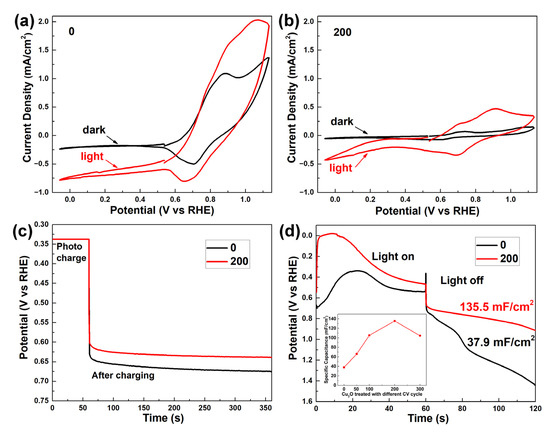
Figure 3.
Cyclic voltammetry scans at 30 mV s−1 of the as-prepared Cu2O (a) and Cu2O treated with 200 voltage cycles (b) in the dark and under illumination. (c) Open-circuit-potential-vs.-time curves of the as-prepared Cu2O and Cu2O treated with 200 voltage cycles after photo-charging at 0.34 VRHE. (d) Galvanostatic photo-charge, dark-discharge curves and corresponding specific capacitance of the as-prepared Cu2O and Cu2O treated with 200 voltage cycles. Inset figure is the specific capacitance plot of Cu2O treated with different voltage cycles. (Electrolyte: 0.5 M Na2SO4 and 0.1 M K2HPO4 aqueous solution, pH = 5).
To assess the photocapacitive performance of the fabricated photocapacitor, different key parameters were measured, as shown in Figure 3c,d. Figure 3c depicts the open-circuit-potential-vs.-time curves. After photo-charging at 0.34 VRHE, an initial open-circuit potential of 0.64 VRHE and 0.60 VRHE were obtained by the as-prepared Cu2O and Cu2O treated with 200 voltage cycles, respectively. Both open-circuit potentials show a good stability with a slow decay rate in the next 5 min, suggesting an effective suppression of oxidating side reaction. Opposite to the hole-storing photocapacitive device, the more negative open-circuit potential of the Cu2O treated with 200 voltage cycles indicates that more electrons were stored in the heterostructure [34]. Figure 3d demonstrates the Galvanostatic photo-charge and dark-discharge curves at a current density of 0.5 mA/cm2. For the as-prepared Cu2O, the photo-charge curve starts with a potential of 0.7 VRHE, corresponding to the reduction potential peak of CuO/Cu2O, as shown in Figure 3a. In the first 20 s, the reduction of CuO is dominant. As the thin CuO layer is reduced to Cu2O, the potential gradually increases from 0.7 VRHE to 0.35 VRHE, and the reduction reaction of Cu2O to Cu occurs, which leads to the potential’s decreasing to 0.5 VRHE. XPS analysis was carried out to investigate the photo-charging process of as-prepared Cu2O. Figure S5a,b show the surface and 3 nm depth XPS profiles of the Cu LMM Auger peak for the as-prepared Cu2O with different photo-charging intervals, respectively. In Figure S5a, the Cu LMM Auger peak at 916.5 eV indicates that Cu+ is the primary state at the surface of the as-prepared Cu2O during the photo-charging process. A peak shifting from 916.5 eV to 918.5 eV is observed in the 3 nm depth XPS profiles of Cu2O after photo-charging for 60 s and 120 s (Figure S5b), confirming the reduction of Cu2O to metallic Cu. These results further suggest that metallic Cu is firstly formed in the bulk rather than on the surface of Cu2O.
For the Cu2O treated with 200 voltage cycles, the photo-charge curve rapidly increases to 0 VRHE, suggesting that the reduction reaction of H+ to H2 is dominant in the first 15 s. As the consumption of absorbed H+ continued, the reduction of CuO to Cu2O became dominant, which leads to the decreasing of potential. According to the literature [26], the reduction reaction of CuO to Cu2O is more favorable than the reduction reaction of Cu2O to Cu, which suppresses the formation of Cu on the Cu2O film treated with 200 voltage cycles. XPS analysis of the Cu2O film treated with 200 voltage cycles after a photo-charging process is shown in Figure S6. No signal of a Cu LMM Auger peak at 918.5 eV for metallic Cu is observed, which further supports the above proposition. In the dark-discharge process, the potential curve of the Cu2O treated with 200 voltage cycles shows a much slower decreasing rate and a 3.5-times higher specific capacitance than that of the as-prepared Cu2O. In the Galvanostatic photo-charge and dark-discharge curve (Figure S7), the bare FTO exhibits a stable potential of −0.66 VRHE and 2.4 VRHE in the photo-charge and dark-discharge process, corresponding to the water reduction and oxidation reaction potential, respectively. Therefore, the FTO substrate does not contribute to the photocapacitive performance of the Cu2O/CuO heterostructure. The inset of Figure 3d demonstrates the gradually increasing specific capacitance from 37.9 mF/cm2 to 135.5 mF/cm2, as surface treatment CV cycles increased from 0 to 200, confirming the electron storage ability of Cu2O/CuO heterostructure. The lower specific capacitance of Cu2O treated with 300 voltage cycles is attributed to the formation of Cu, as confirmed by the XRD results in Figure 2a. It is noted that the specific capacitance of 135.5 mF/cm2 for the Cu2O/CuO heterostructure firstly reported in our work is much higher than that of 20.6 mF/cm2 for the Fe2O3/Ni(OH)2 and 6 mF/cm2 for the BiVO4/PbOx photocapacitors [11,12].
The cycling stability of the Cu2O/CuO heterostructured system is demonstrated in Figure S8. The specific capacitance dropped 83% after the 200 cycle test. Further XPS (Figure S9) and ICP analysis indicate that the deterioration of the CuO layer and an 8.4% leaching of Cu ions into the electrolyte during the cycling test lead to the decrease in specific capacitance. A suitable strategy, such as fabricating a protective layer, is under exploration, to suppress the dissolution of Cu2+ into the electrolyte.
3.3. Photo-Charge and Dark-Discharge Performance of Cu2O/CuO Electrodes in a Two-Electrode System
The photo-charge and dark-discharge current-density curves were measured in a two-electrode system to test the photocapacitive performance under a zero-bias condition. As depicted in Figure 4, both samples show a photo-charge and dark-discharge ability under zero-bias. The as-prepared Cu2O indicates a photo-charge current density of 0.025 mA/cm2 and a dark-discharge current density of 0.013 mA/cm2, higher than that of Cu2O treated with 200 voltage cycles. To explain this phenomenon, the band position and Fermi level of the Cu2O/CuO heterostructure was determined by Mott–Schottky analysis (Figure S10) and UV–vis absorption spectra (Figure S11), according to the method in the literature [35]. As shown in Figure S10, the flat-band potentials of Cu2O and CuO are estimated as 0.46 VRHE and 0.41 VRHE, respectively, both lower than the flat-band potential of bare FTO (0.3 VRHE, Figure S12). The carrier concentrations of Cu2O and CuO are calculated as 6.1 × 1018 cm−3 and 3.1 × 1018 cm−3, respectively. The band gap of Cu2O is about 2.1 eV (Figure S11). As a result, a staggered type-II p–n junction was formed between Cu2O and CuO. As demonstrated in Figure 3a,b, the reduction reaction of H+/H2 cannot happen on both the as-prepared Cu2O and Cu2O treated with 200 voltage cycles under a zero-bias condition. Therefore, the photo-charge and dark-discharge current density observed in Figure 4 is attributed to the redox reaction of Cu2+/Cu+.
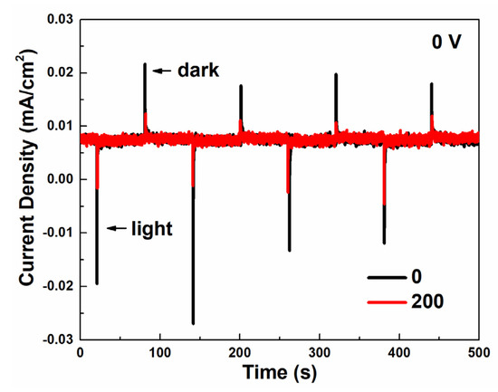
Figure 4.
Two-electrode (Cu2O/Na2HPO4(aq)/Pt) current-density–time (i–t) curves of as-prepared Cu2O and Cu2O treated with 200 voltage cycles through photo-charge and dark-discharge under zero-bias.
Recently, Luo and co-workers developed a novel concept of Faradaic junction [34,36,37,38,39,40]. In photo-rechargeable devices, Faradaic junction provides a platform for ion and electron storage with a carrier-transporting character different from the traditional p–n junction [38]. Adopting this concept, a possible mechanism for the photo-charge and dark-discharge phenomenon on Cu2O/CuO heterostructures under zero-bias is proposed in Figure 5. In our proposal, the CuO layer near the surface of Cu2O works as an n-type semiconductor, while the CuO layer near the electrolyte acts as a Faradaic material, which can store/release the ions and electrons. Under illumination, the quasi-Fermi level in the CuO semiconductor shifts negatively and higher than the Fermi level of the CuO Faradaic layer, which leads to photo-generated electrons in the Cu2O/CuO heterostructure and the H+ ions’ in electrolyte injecting into the CuO Faradaic layer, showing a negative photo-charge current. When the light is off, the Voc in the Cu2O/CuO heterostructure disappears, and the Fermi level in CuO is lower than the Fermi level of the CuO Faradaic layer, causing a positive dark-discharge current. To support this proposal, the Fermi level of the CuO Faradaic layer was measured with a photo-charge and dark-discharge CV scan, showing an equilibrium potential at 0.45 VRHE (Figure S13). The higher photo-charge and dark-discharge current density of the as-prepared Cu2O is attributed to the lower hole–electron recombination rate in a thinner CuO semiconducting layer.
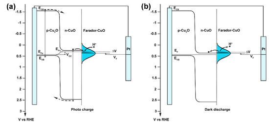
Figure 5.
A proposed mechanism for the (a) photo-charge and (b) dark-discharge phenomenon in Cu2O/CuO photoelectrodes.
4. Conclusions
In summary, a photocapacitive system based on Cu2O/CuO type II heterostructure has been successfully fabricated with a cyclic voltammetric surface treatment of Cu2O photoelectrode. An amorphous CuO layer with a nanosheet structure is formed on the surface of Cu2O after voltage scan cycles. Under solar light illumination, the photo-generated electrons in the conduction band of Cu2O are stored in the CuO layer by reducing CuO to Cu2O, which can be released under a Galvanostatic dark-discharge process. The Cu2O/CuO heterostructure treated with 200 voltage cycles shows a high specific capacitance of 135 mF/cm2 under bias and an open-circuit potential of 0.62 VRHE. The specific capacitance drops 83% after a 200-charge–discharge-cycle test due to the dissolution of the CuO layer. Under a zero-bias condition, the Cu2O/CuO heterostructure demonstrates a photo-charge and dark-discharge current density of 0.02 mA/cm2, in which the CuO layer plays a dual role of n-type semiconductor and Faradaic layer. These results provide guidance for the development of high-performance Cu2O-based photocapacitive devices.
Supplementary Materials
The following supporting information can be downloaded at: https://www.mdpi.com/article/10.3390/en16073231/s1, Figure S1. Surface SEM images of the Cu2O treated with (a) 50, (b) 100, (c) 200 and (d) 300 voltage cycles. Figure S2. The current density versus potential curves for the Cu2O with 200 voltage cycling treatment. Figure S3. The TEM image of Cu2O/CuO heterostructure. Figure S4. The current density versus time curve of the Cu2O treated with 200 voltage cycles. Figure S5. (a) Surface and (b) 3-nm-depth XPS of the Cu LMM Auger peak for as-prepared Cu2O with different photo-charging interval under a current density of −0.5 mA/cm2. Figure S6. (a) Surface and (b) 3-nm-depth XPS of the Cu LMM Auger peak for Cu2O treated with 200 voltage cycles and after photo-charging of 60 s under a current density of −0.5 mA/cm2. Figure S7. Galvanostatic photo-charge, dark-discharge curve of bare FTO. (Current density: 0.5 mA/cm2, Electrolyte: 0.5 M Na2SO4 and 0.1 M K2HPO4 aqueous solution, pH = 5). Figure S8. The photo-charge and dark-discharge cycling stability of the Cu2O treated with 200 voltage cycles. Figure S9. The XPS Cu 2p region from the surface (a) and 3-nm-depth bulk (b) of the Cu2O treated with 200 voltage cycles before and after cycling test. The results show a decreased ratio of Cu2+/Cu+ after cycling test, indicating a deterioration of CuO layer. Figure S10. Mott-Schottky plots measured under different frequency of the as-prepared Cu2O (a) and the Cu2O treated with 200 voltage cycles (b). Figure S11. The plot of (αhv)2 versus hv for the as-prepared Cu2O. Figure S12. The Mott-Schottky plot of bare FTO. Figure S13. Cyclic voltammetry curve of Cu2O treated with 200 voltage cycles in 0.5 M Na2SO4 and 0.1 M K2HPO4 aqueous solution (pH = 5).
Author Contributions
Conceptualization, X.W.; methodology, H.X.; validation, Z.Z.; data curation, H.X., C.F. and H.Z.; writing—original draft, H.X.; writing—review and editing, X.W., R.Z., Y.X. and F.X.; supervision, L.S. All authors have read and agreed to the published version of the manuscript.
Funding
This work is financially supported by the National Natural Science Foundation of China (51802051), the Science and Technology Base and Talent Special Project of Guangxi Province (AD21220137, AD19110032), National Key Research and Development Program (2018YFB1502103, 2018YFB1502105), Joint Funds of the National Natural Science Foundation of China (U20A20237), Chinesisch-Deutsche Kooperationsgruppe: Integrated Computational Materials Engineering of Electrochemical Storage Systems (GZ1528), Guangxi Bagui Scholar Foundation, Guangxi Collaborative Innovation Centre of Structure and Property for New Energy and Materials (2012GXNSFGA06002), the Guangxi Advanced Functional Materials Foundation and Application Talents Small Highlands (Project No. 191010-K).
Data Availability Statement
All data are available upon request from the corresponding author.
Conflicts of Interest
The authors declare no conflict of interest.
References
- Yoshikawa, K.; Kawasaki, H.; Yoshida, W.; Irie, T.; Konishi, K.; Nakano, K.; Uto, T.; Adachi, D.; Kanematsu, M.; Uzu, H.; et al. Silicon Heterojunction Solar Cell with Interdigitated Back Contacts for a Photoconversion Efficiency over 26%. Nat. Energy 2017, 2, 17032. [Google Scholar] [CrossRef]
- Lin, R.; Xu, J.; Wei, M.; Wang, Y.; Qin, Z.; Liu, Z.; Wu, J.; Xiao, K.; Chen, B.; Park, S.M.; et al. All-Perovskite Tandem Solar Cells with Improved Grain Surface Passivation. Nature 2022, 603, 73–78. [Google Scholar] [CrossRef] [PubMed]
- Kim, J.Y.; Lee, J.-W.; Jung, H.S.; Shin, H.; Park, N.-G. High-Efficiency Perovskite Solar Cells. Chem. Rev. 2020, 120, 7867–7918. [Google Scholar] [CrossRef] [PubMed]
- Kokkonen, M.; Talebi, P.; Zhou, J.; Asgari, S.; Soomro, S.A.; Elsehrawy, F.; Halme, J.; Ahmad, S.; Hagfeldt, A.; Hashmi, S.G. Advanced Research Trends in Dye-Sensitized Solar Cells. J. Mater. Chem. A 2021, 9, 10527–10545. [Google Scholar] [CrossRef] [PubMed]
- Sorrentino, R.; Kozma, E.; Luzzati, S.; Po, R. Interlayers for Non-Fullerene Based Polymer Solar Cells: Distinctive Features and Challenges. Energy Environ. Sci. 2021, 14, 180–223. [Google Scholar] [CrossRef]
- Lv, J.; Xie, J.; Mohamed, A.G.A.; Zhang, X.; Wang, Y. Photoelectrochemical Energy Storage Materials: Design Principles and Functional Devices towards Direct Solar to Electrochemical Energy Storage. Chem. Soc. Rev. 2022, 51, 1511–1528. [Google Scholar] [CrossRef] [PubMed]
- Zeng, Q.; Lai, Y.; Jiang, L.; Liu, F.; Hao, X.; Wang, L.; Green, M.A. Integrated Photorechargeable Energy Storage System: Next-Generation Power Source Driving the Future. Adv. Energy Mater. 2020, 10, 1903930. [Google Scholar] [CrossRef]
- Namsheer, K.; Rout, C.S. Photo-Powered Integrated Supercapacitors: A Review on Recent Developments, Challenges and Future Perspectives. J. Mater. Chem. A 2021, 9, 8248–8278. [Google Scholar]
- An, C.; Wang, Z.; Xi, W.; Wang, K.; Liu, X.; Ding, Y. Nanoporous Cu@Cu2O Hybrid Arrays Enable Photo-Assisted Supercapacitor with Enhanced Capacities. J. Mater. Chem. A 2019, 7, 15691–15697. [Google Scholar] [CrossRef]
- Chen, P.; Cao, C.; Ding, C.; Yin, Z.; Qi, S.; Guo, J.; Zhang, M.; Sun, Z. One-Body Style Photo-Supercapacitors Based on Ni(OH)2/TiO2 Heterojunction Array: High Specific Capacitance and Ultra-Fast Charge/Discharge Response. J. Power Sources 2022, 521, 230920. [Google Scholar] [CrossRef]
- Zhu, K.; Luo, W.; Zhu, G.; Wang, J.; Zhu, Y.; Zou, Z.; Huang, W. Interface-Engineered Ni(OH)2/β-like FeOOH Electrocatalysts for Highly Efficient and Stable Oxygen Evolution Reaction. Chem. Asian J. 2017, 12, 2720–2726. [Google Scholar] [CrossRef] [PubMed]
- Safshekan, S.; Herraiz-Cardona, I.; Cardenas-Morcoso, D.; Ojani, R.; Haro, M.; Gimenez, S. Solar Energy Storage by a Heterostructured BiVO4-PbOx Photocapacitive Device. ACS Energy Lett. 2017, 2, 469–475. [Google Scholar] [CrossRef]
- Yuan, Z.-K.; Chen, S.; Xiang, H.; Gong, X.-G.; Walsh, A.; Park, J.-S.; Repins, I.; Wei, S.-H. Engineering Solar Cell Absorbers by Exploring the Band Alignment and Defect Disparity: The Case of Cu- and Ag-Based Kesterite Compounds. Adv. Funct. Mater. 2015, 25, 6733–6743. [Google Scholar] [CrossRef]
- Li, C.; He, J.; Xiao, Y.; Li, Y.; Delaunay, J.-J. Earth-Abundant Cu-Based Metal Oxide Photocathodes for Photoelectrochemical Water Splitting. Energy Environ. Sci. 2020, 13, 3269–3306. [Google Scholar] [CrossRef]
- Wang, Z.; Zhang, L.; Schulli, T.U.; Bai, Y.; Monny, S.A.; Du, A.; Wang, L. Identifying Copper Vacancies and Their Role in the CuO Based Photocathode for Water Splitting. Angew. Chem. Int. Ed. 2019, 58, 17604–17609. [Google Scholar] [CrossRef] [PubMed]
- Yu, Y.-X.; Pan, L.; Son, M.-K.; Mayer, M.T.; Zhang, W.-D.; Hagfeldt, A.; Luo, J.; Grätzel, M. Solution-Processed Cu2S Photocathodes for Photoelectrochemical Water Splitting. ACS Energy Lett. 2018, 3, 760–766. [Google Scholar] [CrossRef]
- Wen, X.; Luo, W.; Zou, Z. Photocurrent Improvement in Nanocrystalline Cu2ZnSnS4 Photocathodes by Introducing Porous Structures. J. Mater. Chem. A 2013, 1, 15479–15485. [Google Scholar] [CrossRef]
- Wen, X.; Luo, W.; Guan, Z.; Huang, W.; Zou, Z. Boosting Efficiency and Stability of a Cu2ZnSnS4 Photocathode by Alloying Ge and Increasing Sulfur Pressure Simultaneously. Nano Energy 2017, 41, 18–26. [Google Scholar] [CrossRef]
- Zhang, R.; Wen, X.; Xu, F.; Zhang, Q.; Sun, L. A Density Functional Theory Study of the Cu2ZnSnS4 Monolayer as a Photo-Electrointegrated Catalyst for Water Splitting and Hydrogen Evolution. J. Phys. Chem. C 2020, 124, 11922–11929. [Google Scholar] [CrossRef]
- Zhang, R.; Wen, X.; Peng, H.; Xia, Y.; Xu, F.; Sun, L. Facet-Dependent CO2 Reduction Reactions on Kesterite Cu2ZnSnS4 Photo-Electro-Integrated Electrodes. Phys. Chem. Chem. Phys. 2022, 24, 48–55. [Google Scholar] [CrossRef]
- Cao, D.; Wang, C.; Zheng, F.; Dong, W.; Fang, L.; Shen, M. High-Efficiency Ferroelectric-Film Solar Cells with an n-Type Cu2O Cathode Buffer Layer. Nano Lett. 2012, 12, 2803–2809. [Google Scholar] [CrossRef] [PubMed]
- Zuo, C.; Ding, L. Solution-Processed Cu2O and CuO as Hole Transport Materials for Efficient Perovskite Solar Cells. Small 2015, 11, 5528–5532. [Google Scholar] [CrossRef] [PubMed]
- Paracchino, A.; Mathews, N.; Hisatomi, T.; Stefik, M.; Tilley, S.D.; Grätzel, M. Ultrathin Films on Copper(I) Oxide Water Splitting Photocathodes: A Study on Performance and Stability. Energy Environ. Sci. 2012, 5, 8673–8681. [Google Scholar] [CrossRef]
- Kim, D.S.; Kim, Y.B.; Choi, J.H.; Suh, H.W.; Lee, H.H.; Lee, K.W.; Jung, S.H.; Kim, J.J.; Deshpande, N.G.; Cho, H.K. Toward Simultaneous Achievement of Outstanding Durability and Photoelectrochemical Reaction in Cu2O Photocathodes via Electrochemically Designed Resistive Switching. Adv. Energy Mater. 2021, 11, 2101905. [Google Scholar] [CrossRef]
- Niu, W.; Moehl, T.; Adams, P.; Zhang, X.; Lefèvre, R.; Cruz, A.M.; Zeng, P.; Kunze, K.; Yang, W.; Tilley, S.D. Crystal Orientation-Dependent Etching and Trapping in Thermally-Oxidised Cu2O Photocathodes for Water Splitting. Energy Environ. Sci. 2022, 15, 2002–2010. [Google Scholar] [CrossRef] [PubMed]
- Amano, F.; Ebina, T.; Ohtani, B. Enhancement of Photocathodic Stability of P-Type Copper(I) Oxide Electrodes by Surface Etching Treatment. Thin Solid Films 2014, 550, 340–346. [Google Scholar] [CrossRef]
- Cendula, P.; Mayer, M.T.; Luo, J.; Grätzel, M. Elucidation of Photovoltage Origin and Charge Transport in Cu2O Heterojunctions for Solar Energy Conversion. Sustain. Energy Fuels 2019, 3, 2633–2641. [Google Scholar] [CrossRef]
- Eisermann, S.; Kronenberger, A.; Laufer, A.; Bieber, J.; Haas, G.; Lautenschläger, S.; Homm, G.; Klar, P.J.; Meyer, B.K. Copper Oxide Thin Films by Chemical Vapor Deposition: Synthesis, Characterization and Electrical Properties. Phys. Status Solidi 2012, 209, 531–536. [Google Scholar] [CrossRef]
- Yang, W.Y.; Kim, W.G.; Rhee, S.W. Radio Frequency Sputter Deposition of Single Phase Cuprous Oxide Using Cu2O as a Target Material and Its Resistive Switching Properties. Thin Solid Film. 2008, 517, 967–971. [Google Scholar] [CrossRef]
- Kardarian, K.; Nunes, D.; Sberna, P.M.; Ginsburg, A.; Keller, D.A.; Pinto, J.V.; Deuermeier, J.; Anderson, A.Y.; Zaban, A.; Martins, R.; et al. Effect of Mg Doping on Cu2O Thin Films and Their Behavior on the TiO2/Cu2O Heterojunction Solar Cells. Sol. Energy Mater. Sol. Cells 2016, 147, 27–36. [Google Scholar] [CrossRef]
- Dubale, A.A.; Pan, C.J.; Tamirat, A.G.; Chen, H.M.; Su, W.N.; Chen, C.H.; Rick, J.; Ayele, D.W.; Aragaw, B.A.; Lee, J.F.; et al. Heterostructured Cu2O/CuO Decorated with Nickel as a Highly Efficient Photocathode for Photoelectrochemical Water Reduction. J. Mater. Chem. A 2015, 3, 12482–12499. [Google Scholar] [CrossRef]
- Paracchino, A.; Brauer, J.C.; Moser, J.E.; Thimsen, E.; Grätzel, M. Synthesis and Characterization of High-Photoactivity Electrodeposited Cu2O Solar Absorber by Photoelectrochemistry and Ultrafast Spectroscopy. J. Phys. Chem. C 2012, 116, 7341–7350. [Google Scholar] [CrossRef]
- Kunturu, P.P.; Huskens, J. Efficient Solar Water Splitting Photocathodes Comprising a Copper Oxide Heterostructure Protected by a Thin Carbon Layer. ACS Appl. Energy Mater. 2019, 2, 7850–7860. [Google Scholar] [CrossRef]
- Zhu, K.; Zhu, G.; Wang, J.; Zhu, J.; Sun, G.; Zhang, Y.; Li, P.; Zhu, Y.; Luo, W.; Zou, Z.; et al. Direct Storage of Holes in Ultrathin Ni(OH)2 on Fe2O3 Photoelectrodes for Integrated Solar Charging Battery-Type Supercapacitors. J. Mater. Chem. A 2018, 6, 21360–21367. [Google Scholar] [CrossRef]
- Huang, S.; Luo, W.; Zou, Z. Band Positions and Photoelectrochemical Properties of Cu2ZnSnS4 Thin Films by the Ultrasonic Spray Pyrolysis Method. J. Phys. D Appl. Phys. 2013, 46, 235108. [Google Scholar] [CrossRef]
- Yin, Z.; Chen, X.; Wang, C.; Guo, Z.; Wu, X.; Zhao, Z.; Yao, Y.; Luo, W.; Zou, Z. Mildly Regulated Intrinsic Faradaic Layer at the Oxide/Water Interface for Improved Photoelectrochemical Performance. Chem. Sci. 2020, 11, 6297–6304. [Google Scholar] [CrossRef]
- Chen, X.; Zhu, K.; Wang, P.; Sun, G.; Yao, Y.; Luo, W.; Zou, Z. Reversible Charge Transfer and Adjustable Potential Window in Semiconductor/Faradaic Layer/Liquid Junctions. iScience 2020, 23, 100949. [Google Scholar] [CrossRef]
- Wang, P.; Chen, X.; Sun, G.; Wang, C.; Luo, J.; Yang, L.; Lv, J.; Yao, Y.; Luo, W.; Zou, Z. A Capacitor-Type Faradaic Junction for Direct Solar Energy Conversion and Storage. Angew. Chem. Int. Ed. 2021, 60, 1390–1395. [Google Scholar] [CrossRef]
- Chen, M.; Dong, H.; Xue, M.; Yang, C.; Wang, P.; Yang, Y.; Zhu, H.; Wu, C.; Yao, Y.; Luo, W.; et al. Faradaic Junction and Isoenergetic Charge Transfer Mechanism on Semiconductor/Semiconductor Interfaces. Nat. Commun. 2021, 12, 6363. [Google Scholar] [CrossRef]
- Wang, P.; Xue, M.; Jiang, D.; Yang, Y.; Zhang, J.; Dong, H.; Sun, G.; Yao, Y.; Luo, W.; Zou, Z. Photovoltage Memory Effect in a Portable Faradaic Junction Solar Rechargeable Device. Nat. Commun. 2022, 13, 2544. [Google Scholar] [CrossRef]


Disclaimer/Publisher’s Note: The statements, opinions and data contained in all publications are solely those of the individual author(s) and contributor(s) and not of MDPI and/or the editor(s). MDPI and/or the editor(s) disclaim responsibility for any injury to people or property resulting from any ideas, methods, instructions or products referred to in the content. |
© 2023 by the authors. Licensee MDPI, Basel, Switzerland. This article is an open access article distributed under the terms and conditions of the Creative Commons Attribution (CC BY) license (https://creativecommons.org/licenses/by/4.0/).