Article

Current Collapse Phenomena Investigation in Automotive-Grade Power GaN Transistors

by
Alfio Basile
1,
Filippo Scrimizzi
1 and
Santi Agatino Rizzo
2,*
1
STMicroelectronics, Stradale Primosole 50, 95121 Catania, Italy
2
Department of Electrical Electronic and Computer Engineering (DIEEI), University of Catania, 95125 Catania, Italy
*
Author to whom correspondence should be addressed.
Energies 2024, 17(1), 230; https://doi.org/10.3390/en17010230
Submission received: 23 November 2023 / Revised: 22 December 2023 / Accepted: 29 December 2023 / Published: 31 December 2023
(This article belongs to the Section F: Electrical Engineering)

Abstract

:
This work analyzes the impact of working conditions on the current collapse (CC) phenomenon for an automotive GaN device. For this purpose, some sensing circuits have been compared to find the most suitable for the considered GaN family. Simulations of the testing schematic have been performed, a prototype board has been created, and some measurements have been taken. Finally, the work has investigated the effect on the CC of the input voltage, current level, switching frequency, and duty cycle. The key outcome is that the temperature increment mitigates the CC phenomenon, which implies that the on-state resistance worsening (dynamic/static ratio), which is due to the CC, reduces with increasing temperature. Therefore, the typical increment of the dynamic on-resistance (RDSON) with increasing temperature is ascribable to the increment of the static one with temperature, while it is not at all an exacerbation of the current collapse phenomenon.

1. Introduction

The automotive market is driving the development of increasingly efficient and high-performance electronic devices. Even today, most of a vehicle’s mechanical components are managed by electronics to optimize driving performance, fuel consumption, efficiency, safety, and driving comfort [1]. Most future power management systems are looking for reductions in both volume occupation and power consumption, but also an improvement of the performance of the systems. Improving the energetic efficiency is the key to increasing devices’ power density and portability [2].
The high electron mobility transistors (HEMTs) are particularly well suited for automotive applications because of their intrinsic properties. The gallium nitride (GaN) power devices are part of the HEMT family. Compared to the silicon power MOSFET, GaN HEMT has some advantages [3]: lower on-resistance ( R D S O N ) at the same breakdown voltage (BV); the channel is a two-dimensional electron gas (2DEG) with high electron mobility ( µ e = 900 ÷ 2000 cm2/Vs); a small R D S O N allows for reducing power losses and increasing GaN-based system efficiency; GaN is a wide bandgap material ( E g = 3.4 eV) with a high critical electric field ( ε c = 3.3 MV/cm); higher BV and small-size devices allow for reducing system size/weight and cost; lower parasitic capacitances and lower gate charge ( Q G ), especially with respect to the Q G D component; and a lower gate charge allows for reducing power consumption and operating at a higher switching frequency. These characteristics allow GaN-based devices to operate at switching frequencies higher than those of silicon, with lower conduction losses. Because of the physical structure of the GaN HEMTs, the bidirectional charge flow is allowed, although GaN HEMTs have no parasitic body diode [4]. Moreover, they are compatible with silicon digital CMOS lateral devices.
The main fields of application of the GaN HEMTs in electric vehicles (EVs) are the high-efficiency on-board charges (OBCs) and the mild hybrid DC–DC converters. Class-D amplifiers and LiDAR (Laser Imaging Detection and Ranging) for autonomous driving are two GaN automotive target applications [5]. GaN-based systems allow to reach high conversion efficiency; the same structure allows bidirectional switching (useful for the OBC) and has a smaller form factor compared to the silicon ones because of the wide bandgap property, so the power density is bigger than that of the silicon-based ones. The applicative boards that adopt GaN HEMTs have reduced dimensions, specifically because the passive elements’ dimensions, like inductors and capacitors, can be reduced [6]. The total cost of the applications based on the GaN transistors is, consequently, smaller than the traditional silicon-based ones.
Most of the devices currently on the market utilize enhancement-mode (e-mode) since they ensure the most reliable and safe operations [7]. Moreover, their driving circuit is simpler to realize. However, the existing technology suffers from some weaknesses, which cannot yet be fixed [8,9]. The worst one is the current collapse (CC) phenomenon, which causes the conduction power consumption to be greater than what the simulations predict [10]. The current collapse leads to an increased on-state resistance, named dynamic R D S O N , because the degradation is due to the device switching [11,12,13].
This paper reports a critical analysis of some sensing–clamping networks for dynamic R D S O N measurements, highlighting their advantages and disadvantages. The network has been chosen considering the compromise among the measurement reliability, circuital complexity and cost. An additional important aspect that drove the choice of the preferred network was the need for measurement automation that, in turn, was necessary to perform many dynamic R D S O N evaluations of different devices under various working conditions. The evaluation of the dynamic_ R D S O N of these devices was necessary to understand the impact of the different working conditions. It is worth noting that, for manufacturers, measurement automation under different working conditions is useful for large-scale device characterization and potential problem appraisal.
As aforementioned, an additional practical outcome of this work concerns the study of the impact of different working conditions. The experimental analyses have highlighted that the dynamic R D S O N increases with increasing the input voltage and switching frequency while it strongly decreases as the duty cycle increases. Instead, the effect of the input current is almost negligible. The most important practical outcome concerns the impact of the temperature on the dynamic R D S O N . In particular, the ratio between dynamic and static R D S O N reduces with increasing temperature. In other words, an increase in the temperature does not exacerbate the current collapse phenomenon; actually, it mitigates the phenomenon itself.
Section 2 first presents a brief introduction of the physical mechanism, then it establishes the main available sensing networks and their main features, and, lastly, highlights some SPICE simulations about the performance of the chosen network working with the complete schematic. The experimental activity is described in Section 3, where the device under test (DUT) is presented and both the static and the dynamic measurements are reported. The conclusion is articulated in Section 4.

2. Analysis of Sensing–Clamping Networks Used for the Evaluation of the Dynamic Resistance in Power GaN Transistors
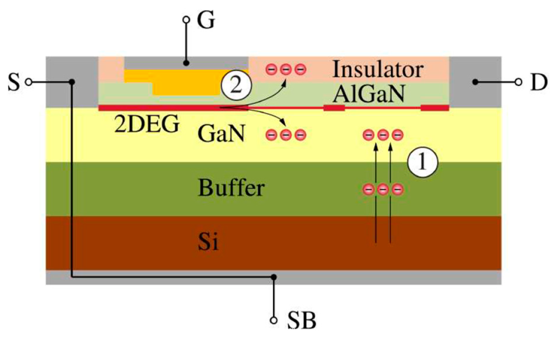
This section first recalls the physics behind the CC phenomenon, then it reports the sensing technique for dynamic R D S O N evaluation and related sensing networks. These techniques indirectly measure the resistance by applying Ohm’s law [14,15]. Consequently, they must accurately know the flowing current of the device, as well as the voltage drop across it. One of the simplest ways to perform the task is to force a known current and then measure the on-state drain-source voltage ( V D S O N ) of the DUT. Since the current collapse phenomenon is related to the charge trapping that dynamically occurs inside its structure, the DUT must switch several times to observe the phenomenon.
The CC is influenced by the following working conditions: off-state voltage ( V I N ); device current ( I I N ); switching condition (hard or soft); switching frequency ( f s ); duty cycle (D); gate resistance ( R g ); gate drive voltage ( V G S ); and junction temperature ( T j ). Figure 1 shows the cross-section of a typical HEMT with a recessed p-GaN gate [16].
The charges are mainly trapped at the two highlighted points: below the gate electrode and inside the GaN/buffer layers.
  • Off-state trapping.
This kind of trapping mechanism is also known as “buffer layer trapping”. It occurs when the transistor, during the off-time interval ( t o f f ), is subjected to the voltage stress V I N : the higher the voltage, the larger the electric field applied between the drain and substrate (1 in Figure 1). In the GaN/buffer layers, the deep-level acceptors are ionized or filled with the leakage electrons from the Si substrate. As the t o f f increases, so does the number of filled traps. As the voltage V I N increases, so does the number of acceptors, hence the amount of trapped electrons.
2.
Hot-electron trapping.
This kind of trapping occurs when the transistor works in hard switching conditions. During the transitory, if the transistor is subjected to both high current and high voltage, the drain region is subjected to a large electric field. The 2DEG electrons acquire sufficient energy to jump toward the GaN/buffer layers where they are trapped by the acceptors (1). Moreover, the electrons are pushed toward the gate-drain region and are trapped in the dielectric (2). The hot electrons trapping depends on the blocking voltage V I N (which affects the electron acceleration and therefore the trapping efficacy) the current I I N (proportional to the number of accelerated electrons) the gate resistance (from which the switching speed is dependent).
Figure 2 reports a generic schematic that can be used to carry out the pulsed I-V characteristic, which is useful for R D S O N estimation. The driver sets the DUT’s switching behavior to the desired frequency and duty cycle. The forcing current ( I I N ) is obtained thanks to the DC voltage V I N and the load resistor R L :
I I N = V I N R L + R D S O N
The diode is used as a freewheeling path when the DUT is off, while the capacitor, C S T O C K , is useful during the transition to the on-state to provide a steep current rising edge. When the DUT is off, it is equivalent to an open circuit, so the drain-source voltage is V D S O F F = V I N and no current flows through it. When the DUT is on, its drain-source voltage drops to V D S O N . The V D S of the DUT undergoes a voltage swing equal to V I N V D S O N , so the full scale of the sensing instrument must be set to include the entire swing. Using an oscilloscope as a sensing instrument, an increase of the V I N implies a reduction of the measurement resolution because of the oscilloscope overdrive phenomenon (OOP) [17,18,19,20]. For this reason, an opportune sensing network (Figure 2) is mandatory to perform an accurate analysis. The sensing network must be connected between the drain and the source of the DUT and an oscilloscope’s probe is connected between its output terminals. In the following, we will refer to the network output voltage as V O U T . Depending on the state in which the DUT is, this additional circuitry plays a different function.
  • When the DUT is off, the network works in clamping mode, clamping the V D S O F F to a V O U T < V I N . Additionally, the clamped voltage must be greater than the V D S O N to avoid clamping during the on-state. This strategy reduces the amplitude of the voltage swing at the output of the network, avoiding the OOP and increasing the measurement resolution.
  • When the DUT is on, the V D S O N is indirectly measured through the network which is working in sensing mode. During this time interval, the ideal output voltage provided by the network V O U T is equal to V D S O N .
At the beginning of the on-state, the network must go quickly in sensing mode to provide an accurate V D S O N measuring. For this reason, the analysis cannot be performed using only a traditional voltage clamping circuit, but one or more components must be included for the measurement purpose. The cost of adding this network is paid in terms of a major circuital complexity and/or possible measurement offset or limitations.
The existing networks differ among them for both
  • the clamping mechanism,
  • the sensing mechanism.

2.1. Description of Sensing-Clamping Networks

2.1.1. Sensing-Clamping Network N.1

The sensing network of Figure 3 contains a Zener diode D 2 , a diode D 1 , and a limiting current resistor R [20,21,22]. The key point of the network is the Zener diode, with its ability to work in the third quadrant, providing quite a stable reverse voltage.
  • Clamping mechanism—The resistor R limits the current from the supply so that the clamped voltage is equal to the sum of D 1 forward voltage ( V f D 1 ) and the Zener voltage of D 2 ( V z D 2 ):
    V O U T = V f D 1 + V z D 2
The task of D 1 is to reduce the sensing delay at the start of the on-state, reducing the equivalent series capacitance (ESC) of the network.
  • Sensing mechanism—When the DUT is on, the output voltage is equal to:
    V O U T = V D S O N V R
    where V R is the offset caused by the leakage current flowing through the resistor. The voltage V O U T follows the V D S O N only after a time interval determined by the RC time constant of the sensing network.

2.1.2. Sensing–Clamping Network N.2

This sensing network [20,21,22,23] consists of a MOSFET depletion transistor M, a resistor R, and a constant voltage V C C (Figure 4). The gate of M is connected to a fixed potential, so its source potential controls its working state.
  • Clamping mechanism—When the DUT is off, the current flows through M toward the resistor R, thus increasing the potential of node A. The voltage is clamped when the transistor is in the subthreshold region. The clamping voltage is then equal to the gate voltage reduced by the MOSFET threshold one ( V M , t h ):
    V O U T = V C C V M , t h
  • Sensing mechanism—When the DUT is on, the current flowing through the sensing network decreases, and so does the potential at node A, bringing M to the on-state. The voltage at the output of the network is
    V O U T = V D S O N V M , D S O N
Even this network introduces a measurement offset, due to the residual current flowing through the network, consisting of the MOSFET on-state voltage ( V M , D S O N ).

2.1.3. Sensing-Clamping Network N.3

This sensing network [20,21,22,23,24,25] combines the two previous networks, adding a few components such as two Schottky diodes D 1 , D 2 , and the resistor R 2 to limit the current that flows through the Zener diode D 3 (Figure 5). M is a MOSFET transistor; V C C , R 1 , and C are, respectively, a DC voltage source, a resistor and a capacitor that set the gate potential and the on-state transient of M.
  • Clamping mechanism—When the DUT is off, the transistor M is in the subthreshold region because the potential at node A increases thanks to the Zener diode D 3 . The clamping process is like the previous one since when M enters the subthreshold region, the network clamps the V D S O F F to
    V O U T = V C C V M , t h
The voltage of V C C is typically increased from 6 V to 8 V to mitigate the amplitude of the transition spikes on the V O U T , avoiding thus the OOP.
  • Sensing mechanism—When the DUT is on, the potential at node A decreases and M is also in on-state. The voltage at the output of the network is
    V O U T = V D S O N V M , D S O N
The two resistors R 1 and R 2 control how the transistor M changes its working state, respectively for the on-state and the off-state.

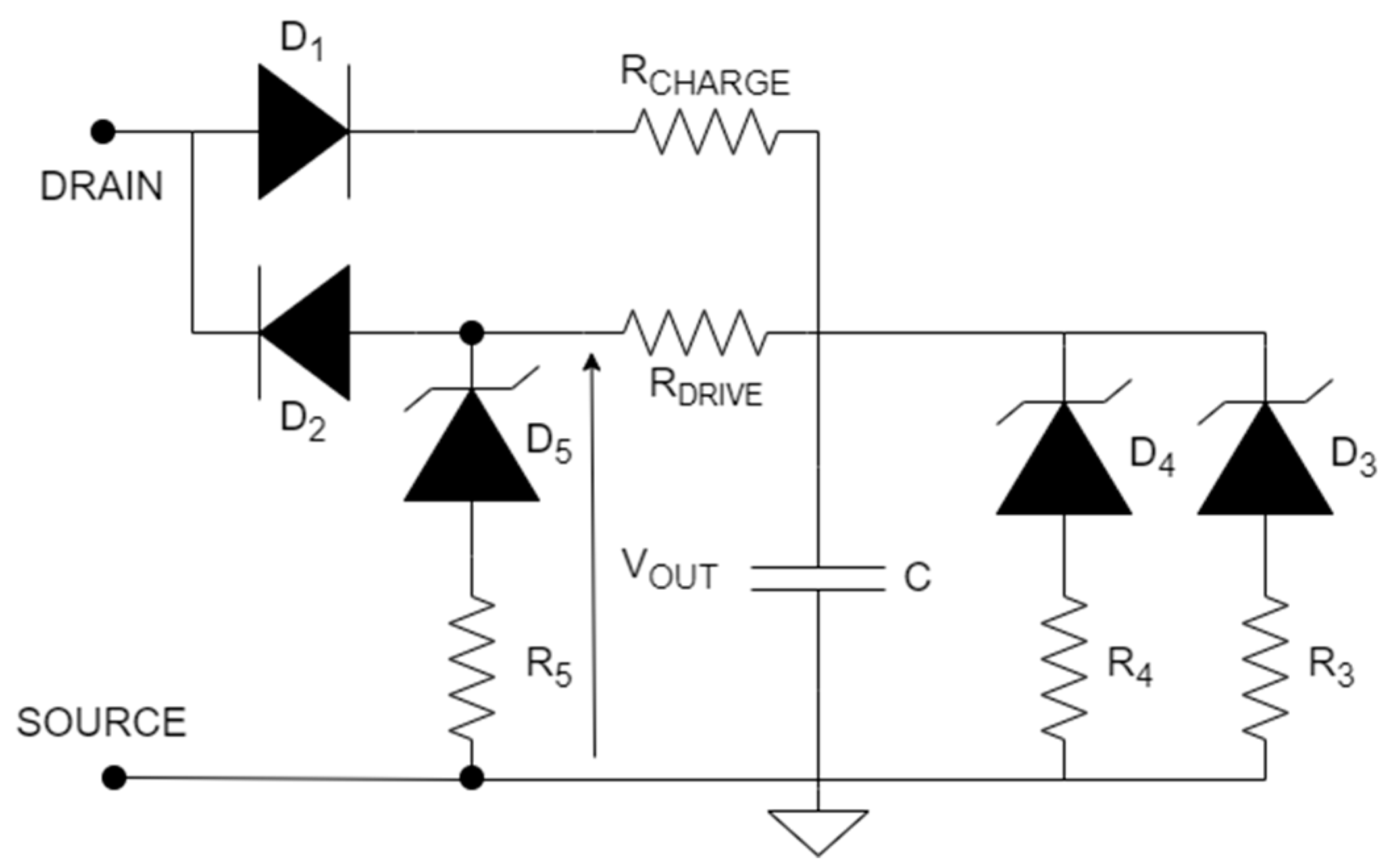
2.1.4. Sensing–Clamping Network N.4

The topology of Figure 6 consists of a current mirror configuration, a load resistor R, a chain of N diodes D C and two high voltage diodes D A and D B , with the same I-V characteristics [18,20,21,22,24]. The series of diodes between nodes A and B is used to clamp the off voltage and could be replaced by a Zener diode.
  • Clamping mechanism—When the DUT is off, the diode D A is reverse-biased, so the mirrored current flows through the series of diodes toward the ground. The current is set by the resistor R. The diode D B is always forward-biased. The clamped voltage, acquired between nodes A and B by a differential probe, is
    V O U T = N V f D C
    where N is the number of diodes in the chain and V f D C is the forward voltage of one diode.
  • Sensing mechanism—When the DUT is on, the two high voltage diodes are forward biased, so the voltage between the network’s output terminals is equal to the DUT on-state one:
    V O U T = V D S O N
It is worth noting that this network could avoid any offset. More specifically, the sensed voltage is not affected by any offset only if the two diodes are perfectly matched between them.

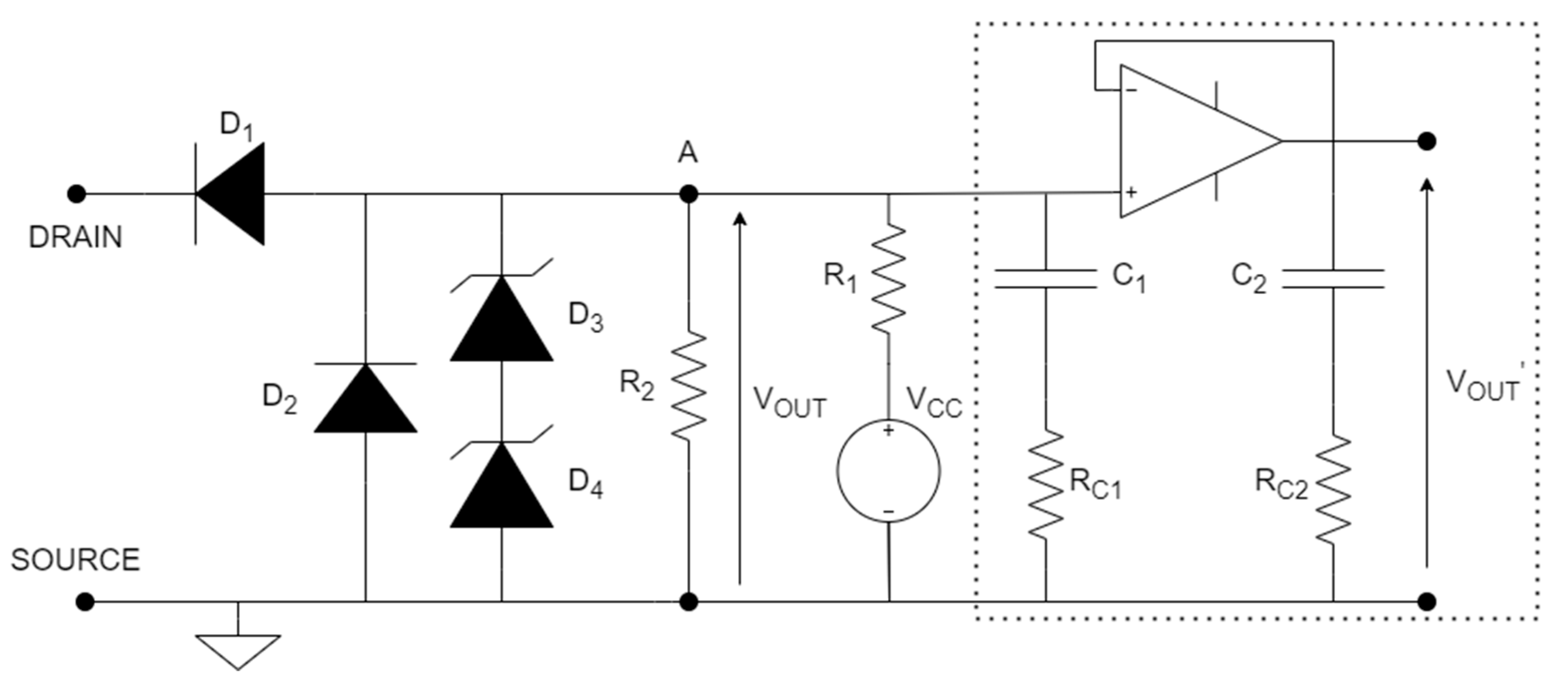
2.1.5. Sensing–Clamping Network N.5

The sensing network [17,21,22,24] consists of only passive components, and is mainly based on two fast switching SiC Schottky diodes, D 1 and D 2 , that work in a complementary way (Figure 7). The other components are two limiting current resistors, R C H A R G E and R D R I V E , a storage capacitor C and three couple of Zener diodes and resistors ( D 3 , D 4 , D 5 , R 3 , R 4 , R 5 ). The output terminal of the circuit is at the cathode of D 5 referred to the ground.
  • Clamping mechanism—When the DUT is off, the current flows through D 1 , while D 2 is reverse biased. The capacitor C is charged during this interval until its voltage is clamped to the Zener voltage of diodes D 3 and D 4 :
    V O U T = V z D 4
  • Sensing mechanism—When the DUT is on, the charges stored in the capacitor flow through R D R I V E toward the DUT, forcing D 2 into conduction. The measured voltage at the output is then equal to
    V O U T = V D S O N + V f D 2
    where V f D 2 is D 2 forward voltage. The resistance R D R I V E is properly chosen to limit the diode’s forward current: a high current may alter its temperature, making temperature dependent on the network’s offset.

2.1.6. Sensing–Clamping Network N.6

The topology [22] consists of two parts (Figure 8): the clamping–sensing circuit, which plays the main function, and the filter circuit inside the dashed square, to reduce the induced ringing noise. Two resistors ( R 1 , R 2 ), two diodes ( D 1 , D 2 ), and two Zener diodes ( D 3 , D 4 ) are the key components of the network.
  • Clamping mechanism—When the DUT is off, the diode D 1 is reverse-biased, so the clamped voltage at node A is obtained from the voltage divider:
    V O U T = V C C R 2 R 1 + R 2
  • Sensing mechanism—When the DUT is on, D 1 is forward-biased, so the output voltage is the sum of the diode forward voltage ( V f D 1 ) and the DUT on-state voltage:
    V O U T = V D S O N + V f D 1
The proper choice of R 1 , R 2 , and V C C is necessary to ensure a clamped voltage greater than V D S O N . The filter circuit consists of an active voltage buffer to reduce the high-frequency oscillations of the power loop. The parasitic inductance and capacitance of the power loop may involve a resonant oscillation that reduces the measurement accuracy. The values of R C 1 and C 1 are properly selected to reduce the ringing. The Zener diodes D 3 and D 4 are used to both reduce the equivalent parasitic capacitance of node A and to clamp the voltage spikes during the transient to the off-state.

2.1.7. Sensing–Clamping Network N.7

This network [24], like some of the previous ones, uses the Zener diode to clamp the off voltage. Moreover, a double isolation branch allows for interrupting the direct path with the DUT (Figure 9). The functional components of this topology are: D 1 , D 2 low capacitance high voltage isolation diodes; D 6 , D 3 freewheeling diodes, with D 6 Zener diode; D4 low value constant current diode; Rt resistor; V C C constant voltage source. The output voltage of the network is acquired between node B and the ground. The branch where V C C and D4 are placed sets the low current used during the entire measurement process.
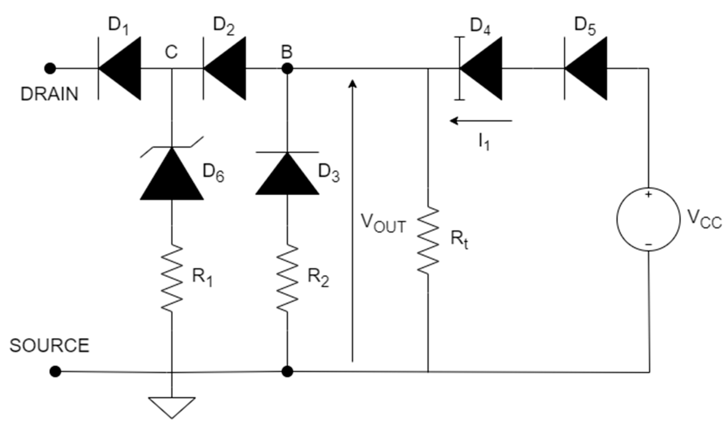
  • Clamping mechanism—When the DUT is off, the two isolation diodes are reverse-biased, so the voltage at node C is clamped at the Zener voltage of D 6 :
    V O U T = V z D 6 + V r D 2 V z D 6
  • Sensing mechanism—At the start of the DUT on-state, the potential of B and C become negative because the junction capacitances of D 1 and D 2 undergo a sudden voltage variation, thus V B and V C are clamped by the freewheeling diodes. Without the two freewheeling diodes, the network’s frequency response would be slower, since it depends on the parasitic capacitance of the four main diodes ( D 1 , D 2 , D 3 , D 6 ). After this initial effect, nodes B and C are charged by the constant current. The R D S O N can be evaluated when the charging of B and C brings the two diodes D 1 and D 2 in forward conduction. When the DUT is completely on, the two isolation diodes are both forward conducting ( V f D 2 is their forward voltage), so the voltage at the output of the sensing network is
    V O U T = V D S O N 2 V f D 2
The sensing offset is concurrently measured during the analysis thanks to the isolation performed by D 1 , thus enabling to nullification of the estimation error due to the sensing offset.
The R D S O N can also be analytically calculated as follows:
R D S O N = V B 2 V f D 2 I R L + I 1 V B R t
The voltages V B and V f D 2 are measured by connecting the oscilloscope’s probes, and the currents I 1 and V B / R t , are imposed by the diodes and the resistor.

2.2. Analysis of Characteristics of the Networks

This subsection presents a critical analysis of the sensing networks described above, primarily highlighting their appeal and limits in the dynamic R D S O N analysis context. The networks described in the previous section differ among them for different aspects, such as measurement offset, sensing delay/switching capability, and maximum voltage to clamp.
Network N.1 is the basic one, both for its functioning and implementation. It is not recommended for medium switching frequency analysis since it brings a non-negligible time delay to the sensing. The network includes only passive components and does not require external sources or batteries. The resistor R must have a high resistance to limit the power dissipation of the network:
P R = V D S O F F V O U T 2 R
Consequently, the time constant of the network is the largest among all others [20] and the network has the worst switching capability. The capacitive contribution to the time constant is lowered by adding the second diode D 2 at the structure. Nevertheless, the frequency improvement is restrained. The network introduces an offset to the measurement due to the leakage current that flows through the resistor R during the sensing time interval.
Network N.2 is the evolution of the first one and it exploits MOSFET’s capability of working as a resistor. This network is faster than the first one to provide the V D S O N measurement in sensing mode, thanks to the MOSFET M. Its main drawback is the voltage spikes induced to V O U T when the DUT enters the subthreshold: the parasitic capacitance of M ( C M , D S ) is affected by a voltage variation, so an extra current on the resistor R generates the voltage spike. This aspect becomes worse as the switching frequency increases or as the resistance R decreases [20]. Moreover, the disturbance propagates through the whole measuring system. The two main consequences are the reduction in measurement accuracy since spikes could induce OOP, and the risk of damaging circuitry and the DUT itself [6,8].
The clamping–sensing network N.3 is a combination of the previous two networks, from which it inherits both the advantages and the drawbacks. Like the previous ones, this topology can be easily implemented, and it is suitable for low on-state voltage measurements. Instead, this circuit is not appropriate for a conduction loss measurement, since during the sensing interval the V O U T shows initial voltage oscillations due to the state transition [24]. Like the second network, it has a high-frequency response and introduces voltage spikes at the beginning of the DUT state changes. This network adds quite negligible voltage offset to the measurement, due to the leakage current that flows through MOSFET M during the sensing interval. The network’s sensing speed depends on the appropriate choice of D 3 and D 1 because D 3 should not conduct when the DUT is turned on. The junction capacitance of D 1 is charged only by the V D S O N , so the system frequency capability depends on how fast D 1 enters the blocking state. The Schottky diodes, the capacitor C and the resistor R 2 are designated to mitigate the voltage spikes, respectively providing a current freewheeling path and a slower transient to the off-state for M [20,23,24]. The amplitude of the spikes can also be reduced by increasing the V C C voltage, but at the cost of a higher clamping voltage. Another important aspect to be considered when choosing the network’s components is that they could easily work out of their safe condition (SOA) when the DUT is subjected to high voltages or it commutates at high frequency [23].
The clamping–sensing network N.4 is based on a current mirror and the two diodes D A and D B . The functioning of the network assumes that D A and D B work exactly at the same working point. Hence a mismatch in the mirror transistors could involve different currents in the two branches, thus producing a measurement offset [23,24]. A second aspect that could decrease the accuracy of the measurement is that a large mirror current influences the voltage drops of the diodes due to a self-heating effect [24]. The use of this topology ensures the highest measurement accuracy and the smallest sensing delays. The output of the circuit is between nodes A and B, so a differential voltage probe is mandatory to correctly read the voltage. Another source of measurement error can be the common mode superimposed at the output. For this reason, the probe’s input amplifier must have a high CMRR. The DUT maximum switching frequency for which this topology can sense is determined by the bandwidth of the differential probe itself.
Network N.5 is thought of as the evolution of N.3 to contain only passive components. The MOSFET transistor is substituted by a capacitor, which stores the charges through the D 1 - R C H A R G E path and releases them during the on the state through the R D R I V E - D 2 path. The key components of this network are D 1 and D 2 , two high-voltage, fast-switching zero recovery SiC Schottky diodes, which allow the circuit to work up to 400 kHz. This network introduces an offset to the measurement consisting of the D 2 forward voltage. The drawback of the network is that the forward current is provided by the energy storage of the capacitor, so it has a decreasing trend that reduces the measurement accuracy [24,25].
The network N.6 clamps the off voltage using a resistive voltage divider. The two resistances ( R 1 , R 2 ) must be chosen to ensure correct clamping only when the DUT is off:
V C C R 2 R 1 + R 2 > V D S O N + V f D 1
This is the only network that takes advantage of a buffer configuration to reduce the ringing of the output node voltage. The frequency capability of the circuit therefore also depends on the bandwidth of the OpAmp. The main frequency limitation comes from the capacitive contribution at node A, because the discharge of the node at the beginning of the on-state is faster when C A is small [22]. Like networks N.3 and N.5, this network also contains the free-wheeling diodes ( D 2 , D 3 , D 4 ) that work during the DUT’s off-state. To increase the frequency capability, D 2 must be a Schottky diode with a low-value junction capacitance, since the output is clamped for a small transient to its negative forward voltage. This topology can provide the correct on-state voltage measurement about 50 ns after the current reaches the load value [22].
The topology N.7 can work at switching frequencies up to 1 MHz [24]. The optimized version of the circuit, with low parasitic capacitance devices, provides the correct on-state voltage 100 ns after the switching. The isolation approach allows for an increase in sensing accuracy thanks to the diode’s differential voltage drop measure. The diode self-heating effect is reduced thanks to D 4 by setting a constant current source of a few milliamps. The two freewheeling diodes, D 6 and D 3 , are chosen with very low parasitic capacitances. The double isolation improves the topology’s frequency response, thanks to the smaller parasitic ESC. The diodes must be chosen with low parasitic capacitance and low reverse recovery time to increase the frequency response of the topology. The clamping mechanism is ensured also for test voltages higher than 600 V. The R D S O N evaluation requires a low-voltage differential probe to measure the V f D 2 . The measurement accuracy is based on the hypothesis that the two insulating diodes exhibit the same characteristic sharing the same forward current. The paper [24] also suggested measuring the voltage at node B using a low-voltage probe with a 1:1 attenuation, thus rejecting background noise and increasing accuracy.
Table 1 reports the main information related to the different Sensing–Clamping networks discussed before. Moreover, the table also reports the main advantages and weak points of the different networks.
The choice of the sensing network to be adopted for the investigation depends on the applicative DUT’s working conditions. The setup of Figure 2 is useful to quantify the current collapse’s effects since it is possible to set the current flowing through the DUT, the off-state voltage stress, and the switching parameters of the driver. The sensing network is chosen based on the compromise between the measurement reliability and circuital complexity: the network N.3 is a low-cost simple circuit, which can quickly provide the R D S O N measure with sufficient accuracy for the analyses to be performed. Furthermore, a SPICE functional simulation of the setup has been executed.

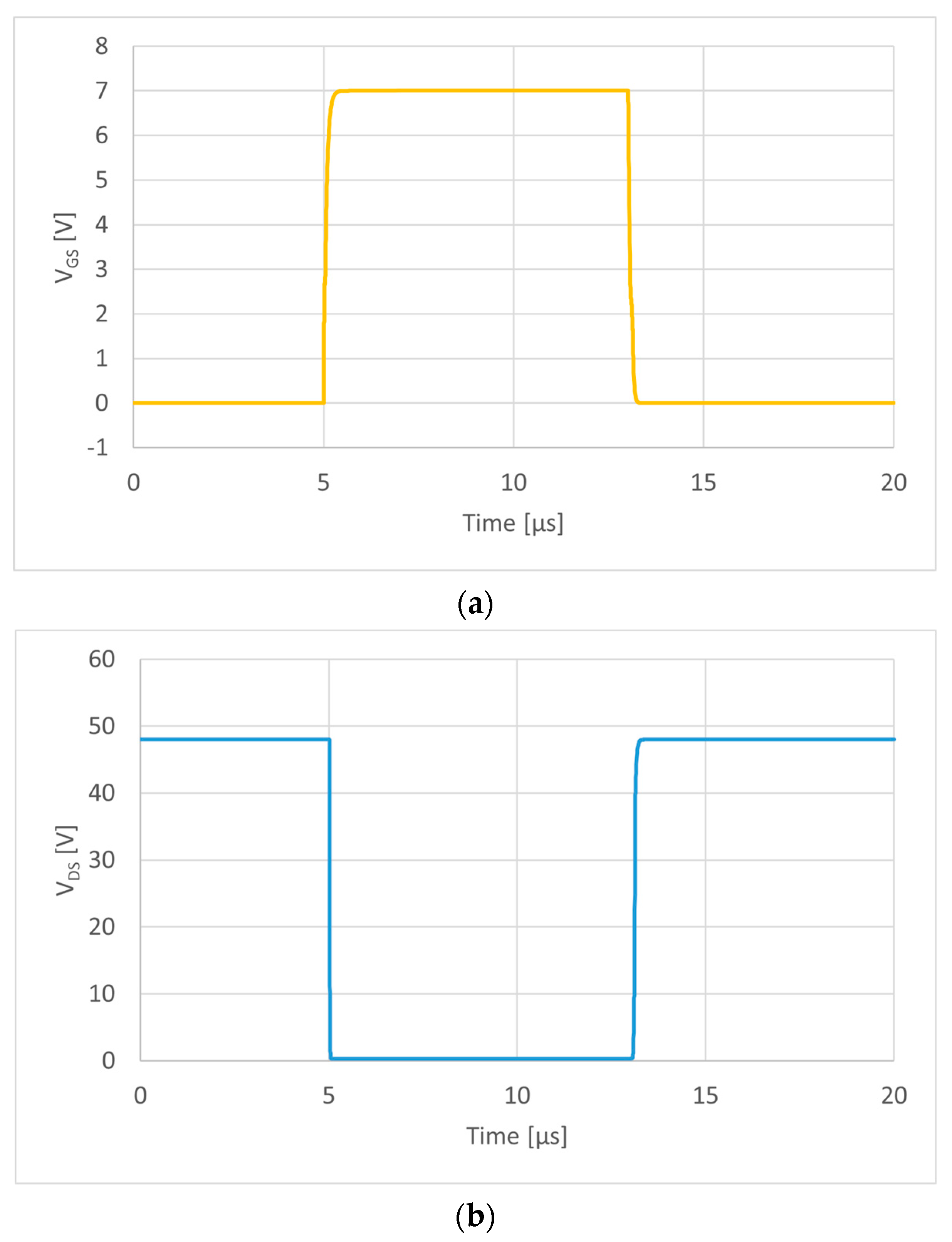
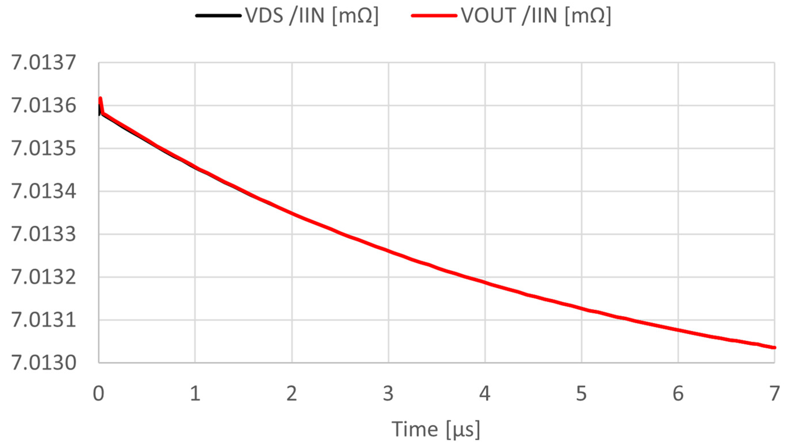
2.3. Test Schematic Simulations

Figure 10 reports the complete schematic adopted for the CC investigation. The basic circuit of Figure 2 is completed by the sensing–clamping network N.3 of Figure 5, connected between the drain-source sensing terminal of the DUT. Moreover, an RC voltage snubber circuit is connected in parallel to the DUT. The snubber is dimensioned to dampen the V D S oscillations during the DUT’s switching transients. Those oscillations could reduce the accuracy of the V D S O N measurement, also limiting the frequency capability of the sensing network. The high side of the half-bridge, not represented here, is shorted to the drain of the low side to prevent it from unwanted turning on.
This subsection shows SPICE simulations of the complete testing circuit represented in Figure 10. The simulations aim to represent the behavior of the sensing network N.3 (Figure 5) inside the testing circuit. The DUT is 7 mΩ 100 V GaN transistor. Its package case temperature ( T c a s e ) is set at 25 °C and it is driven through a gate resistance of 47 Ω. The simulated test conditions are the most recurring one from Table 2: V I N = 48 V, I I N = 48 A, f s = 50 kHz, D = 40%, and T c a s e   = 25 °C.
Figure 11 shows the main waveforms of the simulations, considering the period of the last pulse. These simulations consider only ideal components to provide the functional behavior of the entire circuit, without considering any parasitic elements coming from the circuit layout.
Figure 12 shows the simulated R D S O N behavior during the on-time interval of a pulse. It is obtained dividing the on-state voltage for the current flowing through the DUT. The blue curve is the R D S O N simulated with the V D S O N , the pink curve is obtained by the V O U T from the sensing network. The two curves are perfectly overlapped. It is worth noting that the sensing network N.3 provides the correct R D S O N estimation using only a few passive components and a single MOSFET. This sensing network is most suitable for the test condition, based on the above compromise, without unnecessarily complicating the test schematic.

3. Experimental Activity

This section firstly describes the characterization board upon which the DUT is soldered, then it shows the designed testing board that realizes the testing schematic, then the resuming table with all the testing conditions is presented. Some considerations regarding the board layout are expressed. Finally, the static and the dynamic R D S O N measurements are reported, aiming at analyzing how various working conditions differently affect the R D S O N degradation because of the current collapse. To this aim, the multi-pulse test simulates more realistic working conditions compared to the double-pulse one. The R D S O N evolution is observed from the first pulse to the last.

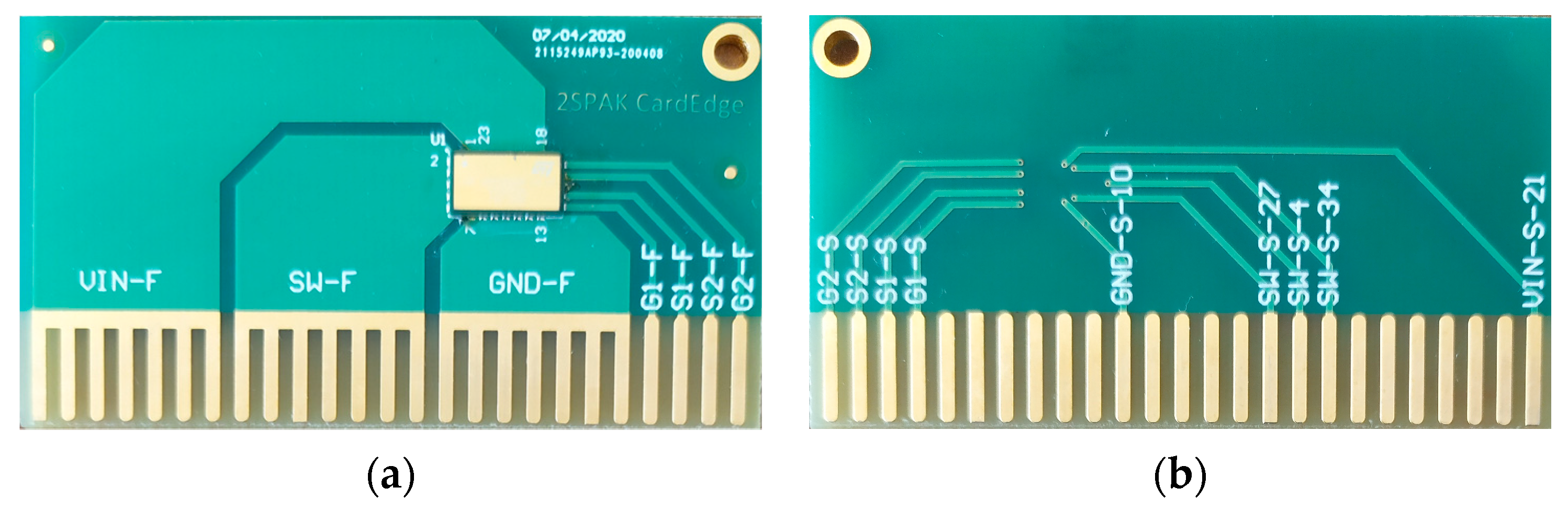
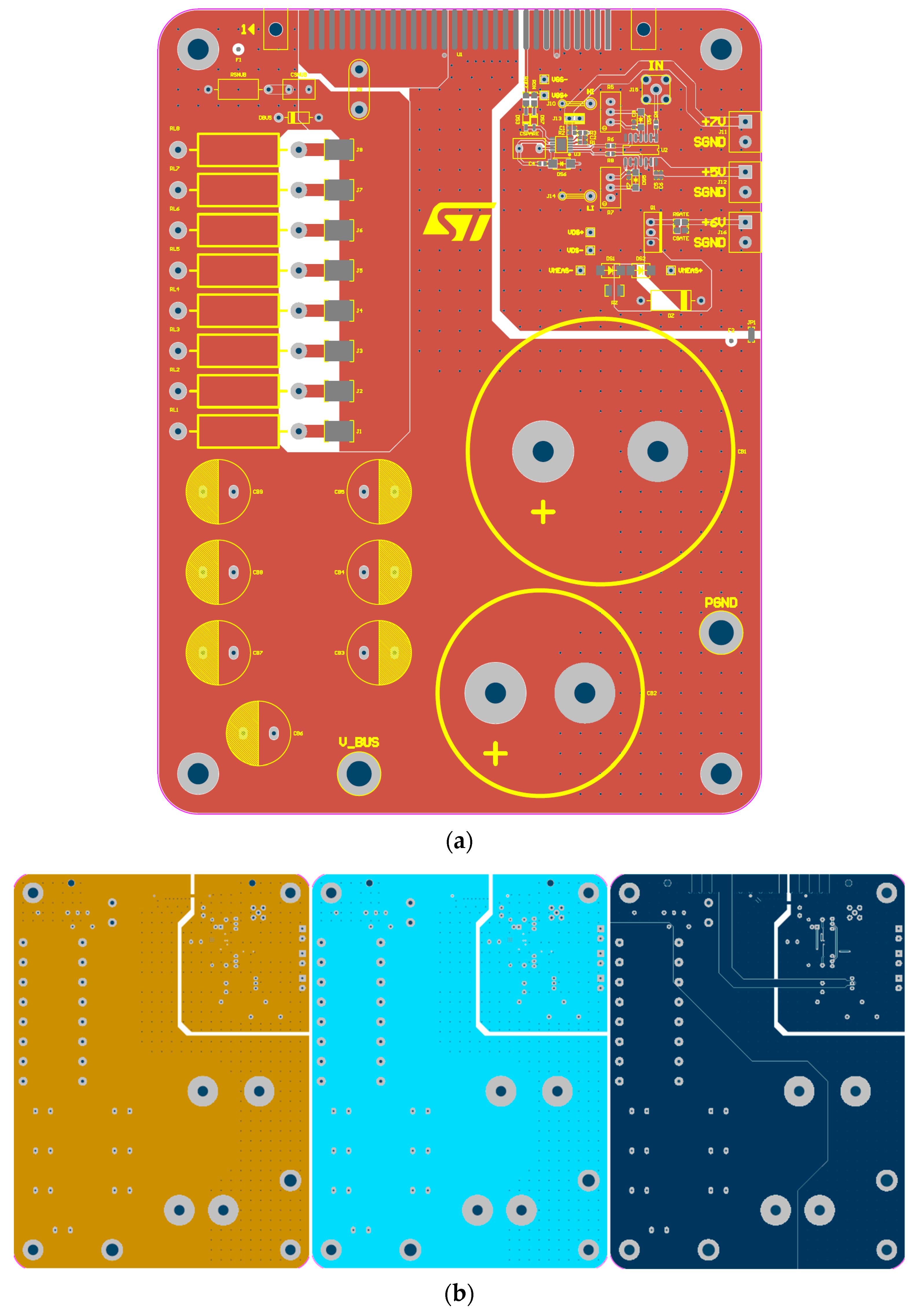
3.1. Experimental Setup and Test Conditions

The DUT is the low-side transistor of a STMicroelectronics half-bridge structure encapsulated in a 2SPACK high-performance package. The half-bridge is 3.5–1.5 mΩ monolithic asymmetric, where the low side has lower R D S O N . Both the high side and the low side share the same silicon substrate.
Figure 13 shows the characterization board, properly designed to carry out the current collapse investigation. All the pins on the high and low sides are accessible. Moreover, a dedicated sense lead is realized for each of them through a via (Figure 13b), which contacts the pad directly under the package. The distinction between the force and the sense pin for the same terminal favors a more accurate voltage measurement through the sense pins.
Figure 14 shows the test board that realizes the schematic in Figure 10. It contains nine electrolytic capacitors connected in parallel, which realize the C S T O C K capacitor; a set of eight load resistors R L , tunable depending on the testing conditions; a thirty-pole connector, where the characterization board is inserted; the sensing network, the driver and the supply, placed in the upper right corner. The driver is an LTC7061, configured to drive only the low-side transistor, supplied between 7 V and the ground. The MOSFET of the sensing network is an STP120NF10, the Zener diode is a BZX55C6V2, and the Schottky are two SMD diodes.
Figure 15 shows a picture of the complete test board. A connector is used to facilitate multiple DUT testing, simply by changing the characterization board. A 1:10 wire transformer is used to read the I I N using a 30A TCP 202 current probe.
The driver control signal is a PWM burst of 100 pulses. The number of commutations is sufficient to trigger the charge-trapping mechanism, allowing current collapse to be observed. The R D S O N measured at the last commutation is representative of the maximum R D S O N . The difference between the maximum R D S O N and the R D S O N of the first pulse represents the R D S O N degradation for the test in question.
Table 2 contains all the test conditions reported in this article. The investigation covers five types of stress conditions: voltage, current, temperature, frequency, and duty cycle. The investigation characterizes the dynamic R D S O N dependence from the analyzed stress conditions, holding all the others. The testing conditions are determined considering the typical working conditions of the transistors, the performances of the sensing network and the characteristics of the board.
One observation regarding the I I N for all the tests: it is obtained as I I N = V I N /( R L + R D S O N ). The C S T O C K capacitor is used to keep constant the V I N during the test window; moreover, C S T O C K is the charge tank that provides instant current to the DUT during the commutations. The sizing of C S T O C K considers the test conditions in Table 2 and the maximum voltage variation V allowed, according to (19):
C S T O C K = I I N D V f s
where D is the duty cycle and f s is the switching frequency. According to (19), the worst-case C S T O C K to provide 48 A current, with a frequency of 30 kHz and D = 40%, with a voltage variation of 50 mV is: C S T O C K ≃ 12.8 mF. The testing board contains more electrolytic capacitors connected in parallel, obtaining a C S T O C K = 36.3 mF.
Bench-top equipment.
  • two GPS 3303 Laboratory DC power supply (30 V/3 A)
  • one TDK-Lambda GEN 80–65 Programmable DC power supply (80 V/65 A)
  • one Keithley 2450 Source Measure Unit (200 V/1 A)
  • one Tektronix AFG 3021C Arbitrary function generator
  • one Tektronix TDS 5054 Digital phosphor oscilloscope (500 MHz)
  • one Tektronix TCP 202 Current probe (30 A)
  • one X-Stream 4300 Thermostream (−80 °C to 225 °C)

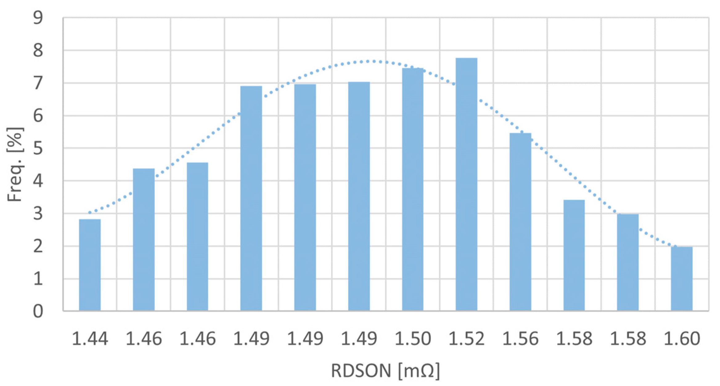
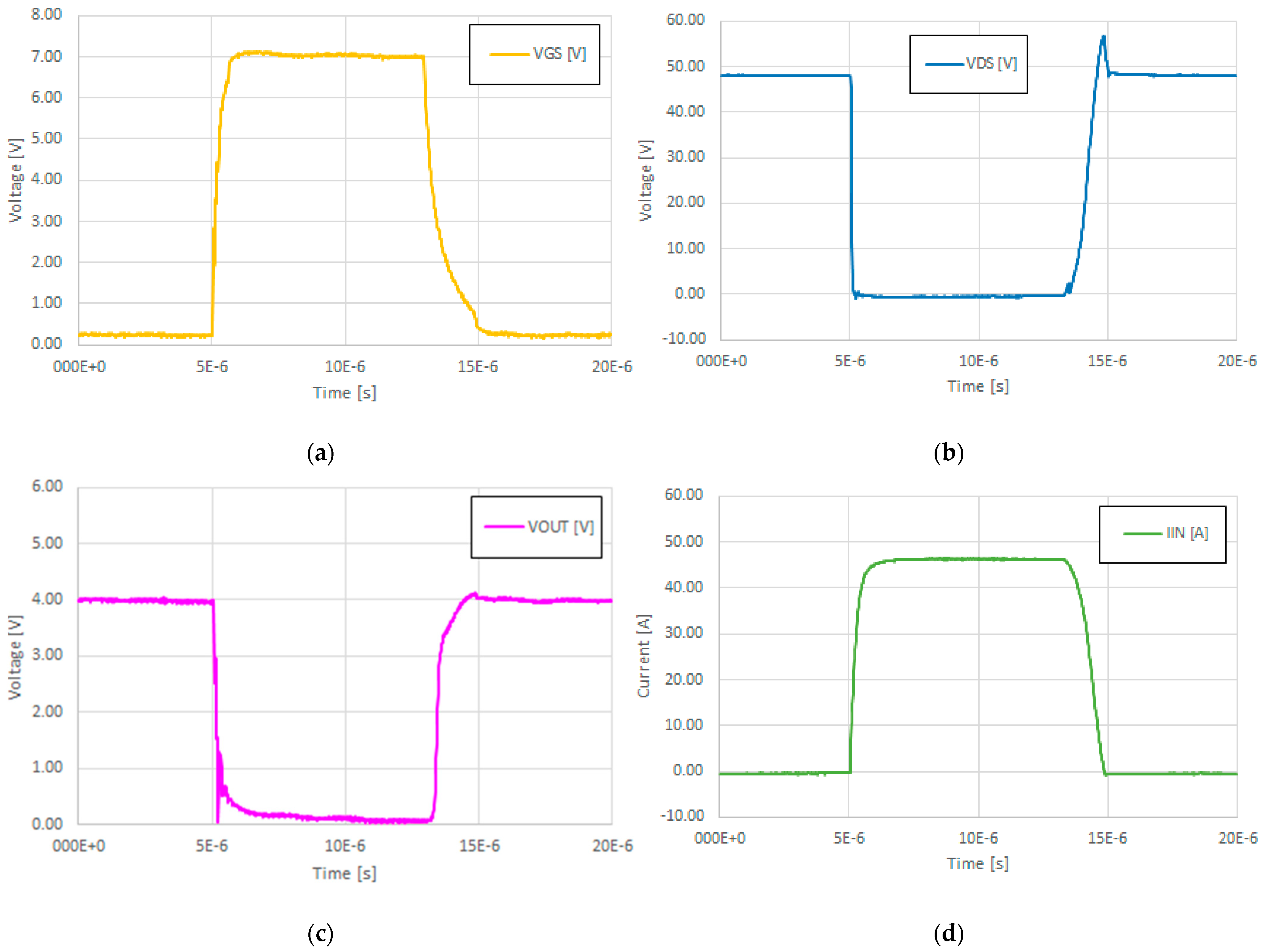
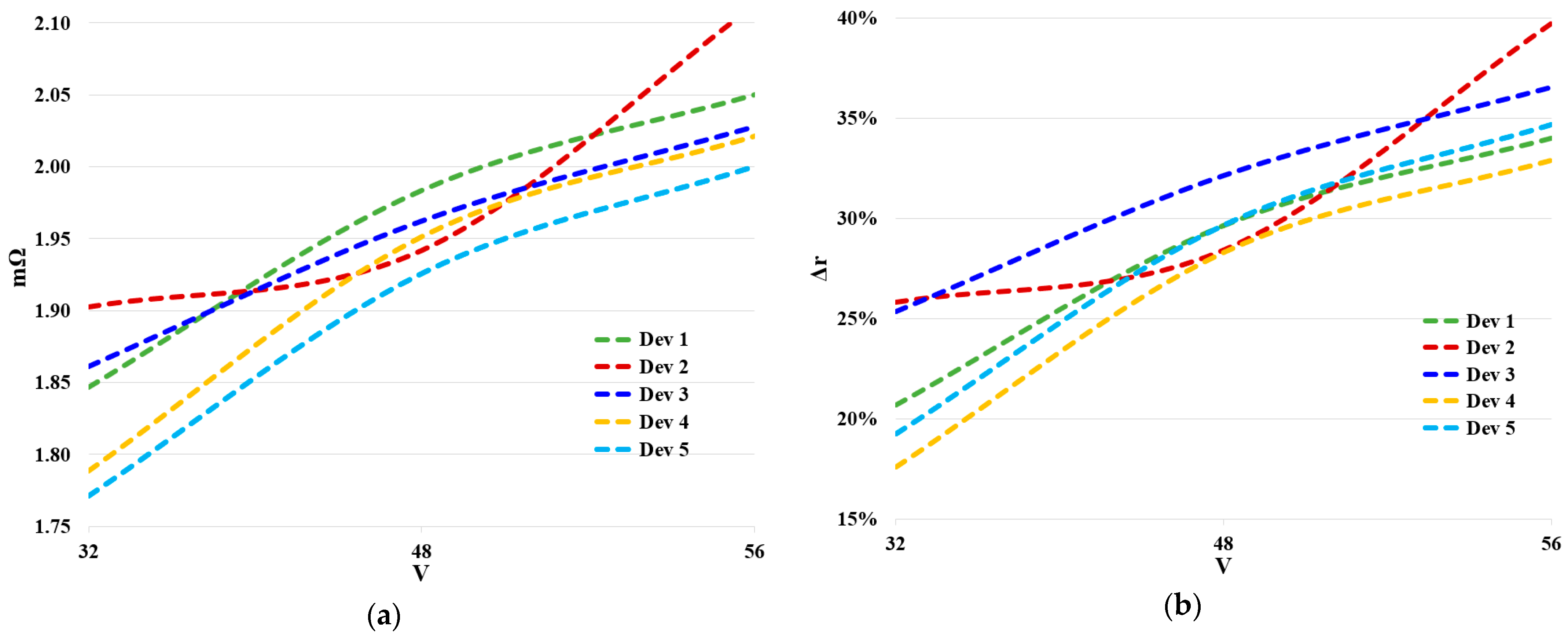
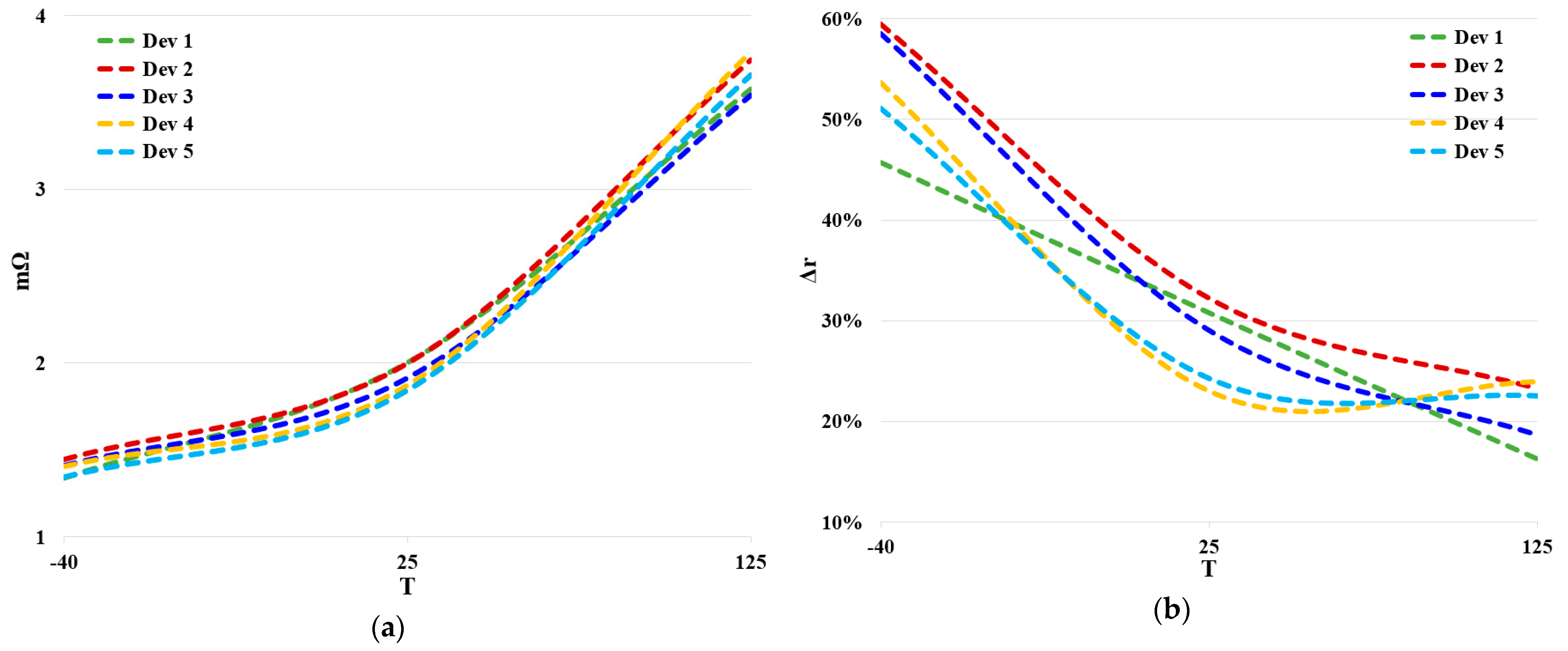
3.2. Experimental Measurements

Static R D S O N measurements provide the reference value for evaluating the dynamic R D S O N degradation for each sample. The static measurements are performed by applying a V G S = 7 V to statically turn on the samples. A sense current of 500 mA is forced through the DUT by a Keithley 2450 SMU, which also reads its V D S O N . Figure 16 shows the distribution of the static R D S O N measurements. The CC would involve a reduction of the slope on the DC output characteristic of the devices.
The static R D S O N mean value is R D S O N = 1.51 mΩ.
Figure 17 shows the waveforms representing a switching period of the following test condition: V I N = 48 V, I I N = 48 A, f s = 50 kHz, D = 40%, and T c a s e = 25 °C. The external temperature of the case is controlled using the Thermostream. The waveforms are related to the hundredth state commutation and represent, respectively, the V G S (yellow waveform), the V D S (blue waveform), the V O U T (pink waveform), and the I I N current flowing through the device (green waveform). Regarding the sensing network, the gate of the transistor M is driven by V C C = 7 V and V M , t h ≈ 3 V. The rising and falling edges of the V G S have been slowed down, in particular the falling one, adopting two different gate resistances to reduce the overvoltage on the V D S during the transition to the off-state (Figure 17b).
During the clamping time interval, when the DUT is off, the simulated V O U T showed in Figure 11c is higher than the measured V O U T (Figure 17c) since, according to (6), the transistor M of the simulation has a lower V M , t h .
In the following, the dynamic R D S O N measured for five devices under various test conditions is reported. In particular, the working conditions of Table 2 have been considered.
For each device, a comparison with the static R D S O N is also reported to effectively analyze the impact of the working conditions on the dynamic R D S O N . To this aim the increment of R D S O N has been evaluated as follows:
r = R D S O N . d y n a m i c R D S O N . s t a t i c R D S O N . d y n a m i c %
The values of the static R D S O N are reported in Table 3 for different temperatures.
Figure 18, Figure 19, Figure 20, Figure 21 and Figure 22 report the values of the dynamic R D S O N for various device and different working conditions (Table 2). Hence, each figure reports the effect of a single quantity variation since the others are kept constant. The resistance variation, Δ r , with respect to the static R D S O N is also reported for each device to better highlight the effect of the single quantity. Considering that the static R D S O N increases with the temperature, Δ r is calculated at the same temperature to effectively evaluate the effect of temperature on the current collapse phenomenon.
The figures highlight the fact that the dynamic R D S O N increases with an increasing input voltage (Figure 18) and switching frequency (Figure 21), while it strongly decreases as the duty cycle increases (Figure 22). These results are in accordance with the literature.
The increment of the input voltage involves a higher voltage across the device during the off-time and the turn-on. Thus, it negatively impacts the dynamic value since it empowers the off-state and hot-electrons trapping.
The increment of the switching frequency for a given duty cycle or the reduction of the duty cycle for a given frequency involves a reduction of the on-time. Considering that, as the device starts to conduct the carriers are partially removed also by the flowing current, the reduction of the on-time implies lessening the recombination of the trapped charges, thus more charges in the channel imply greater dynamic R D S O N . Additionally, the off-time increases if the on-time is reduced. Considering that during the off-time one of the two trapping mechanisms occurs, the increment of the off-time also involves an increment of the dynamic R D S O N . Therefore, both phenomena concurrently entail the increment of the dynamic R D S O N as highlighted in Figure 21 and Figure 22.
The effect of the input current (Figure 19) is almost negligible for all the devices. The effect of the current is affected by the other operating conditions and by the specific device family. The increment of the current enhances the aforementioned recombination phenomenon, thus pushing toward a dynamic R D S O N reduction. On the other hand, a larger current during the turn-on empowers the hot-trapping phenomenon, thus involving a dynamic R D S O N raise. Considering that varying the input current does not involve substantial dynamic R D S O N variation in all the tested devices, it follows that for this family—and the set test conditions—the two opposite phenomena compensate each other.
The results in Figure 20 seem contradictory since the dynamic R D S O N increases as the temperature increases (Figure 20a) but the increment of the dynamic compared to the static R D S O N , Δ r , reduces as the temperature increases (Figure 20b). In the literature, it is usually reported an increase of the dynamic R D S O N with increasing temperature, thus it seems that the information in Figure 20a is more valuable. However, such an approach is strongly reductive because it focuses on the dynamic value only, which is of interest only in terms of conduction losses increment in comparison to the one expected when the static one is considered. Therefore, the most important information is reported in Figure 20b, which shows that the ratio between dynamic and static R D S O N reduces with increasing temperature. In other words, an increment in the temperature does not exacerbate the current collapse phenomenon; rather, it mitigates the phenomenon.

4. Conclusions

This paper has first revised some sensing techniques for dynamic R D S O N evaluation and related sensing networks for selecting the best one in relation to the specific automotive grade GaN family to be investigated. The choice has considered an optimal compromise among measurement reliability, circuital complexity, and cost. Moreover, the networks suitability for mass experimental test has been also considered. The selected measurement system has been adopted for analyzing the effect of the working conditions on the dynamic R D S O N . The results highlight that the dynamic R D S O N increases with increasing input voltage and switching frequency while it decreases as the duty cycle increases. The current does not have an appreciable effect, while a temperature increment increases the dynamic R D S O N , although it positively affects the current collapse phenomenon.

Author Contributions

All authors contributed equally to the work. All authors have read and agreed to the published version of the manuscript.

Funding

This research was partially funded by “Ministero dell’Istruzione dell’Università e della Ricerca” under the call PRIN 2017 grant number 2017MS9F49—Project “Advanced power-trains and systems for full electric aircrafts”.

Conflicts of Interest

The authors declare no conflict of interest.

References

  1. Matallana, A.; Ibarra, E.; López, I.; Andreu, J.; Garate, J.I.; Jordà, X.; Rebollo, J. Power module electronics in HEV/EV applications: New trends in wide-bandgap semiconductor technologies and design aspects. Renew. Sustain. Energy Rev. 2019, 113, 109264. [Google Scholar] [CrossRef]
  2. Wen, J.; Zhao, D.; Zhang, C. An overview of electricity powered vehicles: Lithium-ion battery energy storage density and energy conversion efficiency. Renew. Energy 2020, 162, 1629–1648. [Google Scholar] [CrossRef]
  3. Keshmiri, N.; Wang, D.; Agrawal, B.; Hou, R.; Emadi, A. Current Status and Future Trends of GaN HEMTs in Electrified Transportation. IEEE Access. 2020, 8, 70553–70571. [Google Scholar] [CrossRef]
  4. Liu, Y.; Yang, S.; Han, S.; Sheng, K. Investigation of Surge Current Capability of GaN E-HEMTs in The Third Quadrant: The Impact of P-GaN Contact. IEEE J. Emerg. Sel. Top. Power Electron. 2019, 7, 1465–1474. [Google Scholar] [CrossRef]
  5. Scrimizzi, F.; Cammarata, F.; D’Agata, G.; Nicolosi, G.; Musumeci, S.; Rizzo, S.A. The GaN Breakthrough for Sustainable and Cost-Effective Mobility Electrification and Digitalization. Electronics 2023, 12, 1436. [Google Scholar] [CrossRef]
  6. Zhao, X.; Chen, C.W.; Lai, J.S.; Yu, O. Circuit Design Considerations for Reducing Parasitic Effects on GaN-Based 1-MHz High-Power-Density High-Step-Up/Down Isolated Resonant Converters. IEEE J. Emerg. Sel. Top. Power Electron. 2019, 7, 695–705. [Google Scholar] [CrossRef]
  7. Pushpakaran, B.N.; Subburaj, A.S.; Bayne, S.; Commercial, B. GaN-Based Power Electronic Systems: A Review. J. Electron. Mater. 2020, 49, 6247–6262. [Google Scholar] [CrossRef]
  8. Meneghesso, G.; Meneghini, M.; Zanoni, E. Power GaN Devices Materials, Applications and Reliability; Springer: Cham, Switzerland, 2016. [Google Scholar]
  9. Kozak, J.P.; Zhang, R.; Porter, M.; Song, Q.; Liu, J.; Wang, B.; Wang, R.; Saito, W.; Zhang, Y. Stability, Reliability, and Robustness of GaN Power Devices: A Review. IEEE Trans. Power Electron. 2023, 38, 8442–8471. [Google Scholar] [CrossRef]
  10. Mauromicale, G.; Rizzo, S.A.; Salerno, N.; Susinni, G.; Raciti, A.; Fusillo, F.; Palermo, A.; Scollo, R. Analysis of the impact of the operating parameters on the variation of the dynamic on-state resistance of GaN power devices. In Proceedings of the 2020 2nd IEEE International Conference on Industrial Electronics for Sustainable Energy Systems (IESES), Cagliari, Italy, 1–3 September 2020; Volumre 1, pp. 101–106. [Google Scholar]
  11. Vetury, R.; Zhang, N.Q.; Keller, S.; Mishra, U.K. The impact of surface states on the DC and RF characteristics of AlGaN/GaN HFETs. IEEE Trans. Electron Devices 2001, 48, 560–566. [Google Scholar] [CrossRef]
  12. Gill, L.; DasGupta, S.; Neely, J.C.; Kaplar, J.R.; Michaels, A.J. A Review of GaN HEMT Dynamic ON-Resistance and Dynamic Stress Effects on Field Distribution. IEEE Trans. Power Electron. 2024, 39, 517–537. [Google Scholar] [CrossRef]
  13. Johwoo, J.; del Alamo, J.A.; Jimenez, J. A simple current collapse measurement technique for GaN high-electron mobility transistors. IEEE Electron Device Lett. 2008, 29, 665–667. [Google Scholar]
  14. Alemanno, A.; Santarelli, A.; Sangiorgi, E.; Florian, C. Characterization of the Dynamic RON of 600 V GaN Switches under Operating Conditions. Electronics 2023, 12, 943. [Google Scholar] [CrossRef]
  15. Zhu, H.; Matioli, E. Accurate Measurement of Dynamic ON-Resistance in GaN Transistors at Steady-State. IEEE Trans. Power Electron. 2023, 38, 8045–8050. [Google Scholar] [CrossRef]
  16. Zulauf, G.; Guacci, M.; Kolar, J.W. Dynamic on-resistance in GaN-on-Si HEMTs: Origins, dependencies, and future characterization frameworks. IEEE Trans. Power Electron. 2019, 35, 5581–5588. [Google Scholar] [CrossRef]
  17. Badawi, N.; Hilt, O.; Bahat-Treidel, E.; Böcker, J.; Würfl, J.; Dieckerhoff, S. Investigation of the Dynamic On-State Resistance of 600 V Normally-Off and Normally-On GaN HEMTs. IEEE Trans. Ind. Appl. 2016, 52, 4955–4964. [Google Scholar] [CrossRef]
  18. de Oliveira, E.F.; Noeding, C.; Zacharias, P. Impact of dynamic on-resistance of high voltage GaN switches on the overall conduction losses. In Proceedings of the PCIM Europe 2017; International Exhibition and Conference for Power Electronics, Intelligent Motion, Renewable Energy and Energy Management, VDE, Nuremberg, Germany, 16–18 May May 2017; pp. 1–8. [Google Scholar]
  19. Cai, Y.; Forsyth, J.A.; Todd, R. Impact of GaN HEMT dynamic on-state resistance on converter performance. In Proceedings of the 2017 IEEE Applied Power Electronics Conference and Exposition (APEC), Tampa, FL, USA, 26–30 March 2017; pp. 1689–1694. [Google Scholar]
  20. Gelagaev, R.; Jacqmaer, P.; Driesen, J. A fast voltage clamp circuit for the accurate measurement of the dynamic on-resistance of power transistors. IEEE Trans. Ind. Electron. 2014, 62, 1241–1250. [Google Scholar] [CrossRef]
  21. Badawi, N.; Dieckerhoff, S. A new method for dynamic Ron extraction of GaN power HEMTs. In Proceedings of the PCIM Europe 2015, International Exhibition and Conference for Power Electronics, Intelligent Motion, Renewable Energy and Energy Management, VDE, Nuremberg, Germany, 19–20 May 2015; pp. 1–6. [Google Scholar]
  22. Yang, F.; Xu, C.; Akin, B. Experimental evaluation and analysis of switching transient’s effect on dynamic on-resistance in GaN HEMTs. IEEE Trans. Power Electron. 2019, 34, 10121–10135. [Google Scholar] [CrossRef]
  23. Qiuping, Y.; Zhibin, Z.; Peng, S.; Bin, Z.; Yumeng, C. An improved voltage clamp circuit suitable for accurate measurement of the conduction loss of power electronic devices. Sensors 2021, 21, 4285. [Google Scholar]
  24. Lei, J.; Wang, R.; Yang, G.; Wang, J.; Jiang, F.; Chen, D.; Lu, H.; Zhang, R.; Zheng, Y. Precise Extraction of Dynamic Rdson Under High Frequency and High Voltage by a Double-Diode-Isolation Method. IEEE J. Electron Devices Soc. 2019, 7, 690–695. [Google Scholar] [CrossRef]
  25. Lu, B.; Palacios, T.; Risbud, D.; Bahl, S.; Anderson, D.I. Extraction of dynamic on-resistance in GaN transistors: Under soft-and hard-switching conditions. In Proceedings of the 2011 IEEE Compound Semiconductor Integrated Circuit Symposium (CSICS), Waikoloa, HI, USA, 16–19 October 2011; pp. 1–4. [Google Scholar]
Figure 1. Charge-trapping collocation in p-GaN recessed gate HEMT. Credit by [16].
Energies 17 00230 g001
Figure 2. Basic circuit for R D S O N estimation.
Energies 17 00230 g002
Figure 3. Sensing–Clamping network N.1.
Energies 17 00230 g003
Figure 4. Sensing–Clamping network N.2.
Energies 17 00230 g004
Figure 5. Sensing-Clamping network N.3.
Energies 17 00230 g005
Figure 6. Sensing–Clamping network N.4.
Energies 17 00230 g006
Figure 7. Sensing–Clamping network N.5.
Energies 17 00230 g007
Figure 8. Sensing–Clamping network N.6.
Energies 17 00230 g008
Figure 9. Sensing–Clamping network N.7.
Energies 17 00230 g009
Figure 10. Schematic for CC investigation.
Energies 17 00230 g010
Figure 11. Simulated waveforms of a single pulse: (a) V G S ; (b) V D S (c) V O U T ; (d) I I N .
Energies 17 00230 g011aEnergies 17 00230 g011b
Figure 12. Simulated R D S O N behavior with/without the sensing network.
Energies 17 00230 g012
Figure 13. Shown is 2SPAK package soldered on the characterization board: (a) top side; (b) bottom side.
Energies 17 00230 g013
Figure 14. Test board layout: (a) top layer (red); (b) mid-layers (golden-light blue) and bottom layer (dark blue).
Energies 17 00230 g014
Figure 15. Complete testing board.
Energies 17 00230 g015
Figure 16. Static R D S O N normal distribution.
Energies 17 00230 g016
Figure 17. Waveforms of a single pulse: (a) V G S ; (b) V D S (c) V O U T ; (d) I I N .
Energies 17 00230 g017
Figure 18. Impact of the input voltage on the dynamic R D S O N for various devices: (a) resistance values; (b) resistance variation in comparison with the static R D S O N measured at room temperature.
Energies 17 00230 g018
Figure 19. Impact of the input current on the dynamic R D S O N for various devices: (a) resistance values; (b) resistance variation in comparison with the static R D S O N measured at room temperature.
Energies 17 00230 g019
Figure 20. Impact of the operating temperature on the dynamic R D S O N for various devices: (a) resistance values; (b) resistance variation in comparison with the static R D S O N measured at the same temperature of the dynamic one.
Energies 17 00230 g020
Figure 21. Impact of the switching frequency on the dynamic R D S O N for various devices: (a) resistance values; (b) resistance variation in comparison with the static R D S O N measured at room temperature.
Energies 17 00230 g021
Figure 22. Impact of the duty cycle on the dynamic R D S O N for various devices: (a) resistance values; (b) resistance variation in comparison with the static R D S O N measured at room temperature.
Energies 17 00230 g022
Table 1. Sensing–Clamping networks comparison.
NetworkBased onMax VoltageExternal SourceProbe TypeAdvantagesWeakness
Figure 3Zener diodeNoNopassive
  • Minimal circuit
  • Low V O U T , O F F
  • Lowest switching capability
  • Trade-off between the measurement offset and the power dissipation on R
Figure 4transistor600 V8 Vpassive
  • Minimal circuit
  • High switching capability
  • Reduced resolution due to the induced spikes on the V O U T
Figure 5transistor600 V8 Vpassive
  • High switching capability
  • Trade-off between the clamped voltage and the voltage spikes on V O U T
  • Strictly working conditions may make the components work out of their SOA
Figure 6diode300 V5 Vdifferential
  • No measuring offset
  • Fast switching between clamping–sensing modes
  • High bandwidth and CMRR, low voltage differential voltage probe required
Figure 7SiC diode600 VNopassive
  • Passive components only
  • No ext. voltage supply
  • High switching capability
  • Switching capability strictly depends on the properties of the SiC diodes
Figure 8resistor 15 Vpassive
  • Lowest V O U T ringing noise, thanks to the filter circuit
  • High switching capability
  • Non-minimal circuit
  • D 2 dependent switching capability
Figure 9diode650 V5 Vdifferential
  • High switching capability
  • High measurement accuracy
  • Non-minimal circuit
  • Differential voltage probe required
Table 2. Test conditions. To analyze the effect of each quantity, it is varied as reported below while keeping constant the others.
Test Condition V I N I I N TemperatureFrequencyDuty Cycle
Tested Quantity
V I N 32 V48 A25 °C50 kHz40%
48 V
56 V
I I N 48 V32 A25 °C50 kHz40%
48 A
56 A
70 A
Temperature48 V48 A−40 °C50 kHz40%
25 °C
125 °C
Frequency48 V48 A25 °C30 kHz40%
40 kHz
50 kHz
70 kHz
80 kHz
Duty cycle48 V48 A25 °C50 kHz15%
20%
30%
40%
50%
Table 3. Static R D S O N (mΩ) of the tested device at room temperature and extreme operating temperature.
T c a s e Dev 1Dev 2Dev 1Dev 1Dev 1
−40 °C1.0251.0130.9951.0190.995
25 °C1.531.5121.4851.5211.485
125 °C3.0753.0392.9853.0572.985
Disclaimer/Publisher’s Note: The statements, opinions and data contained in all publications are solely those of the individual author(s) and contributor(s) and not of MDPI and/or the editor(s). MDPI and/or the editor(s) disclaim responsibility for any injury to people or property resulting from any ideas, methods, instructions or products referred to in the content.

