Article

Optimizing Insulated-Gate Bipolar Transistors’ Lifetime Estimation: A Critical Evaluation of Lifetime Model Adjustments Based on Power Cycling Tests

1
Institute for Materials Research and Imec Division Imomec (IMO-IMOMEC), Hasselt University, Wetenschapspark 1, 3590 Diepenbeek, Belgium
2
Interuniversity Microelectronics Center (IMEC), Kapeldreef 75, 3001 Heverlee, Belgium
3
EnergyVille, Thor Park 8310, 3600 Genk, Belgium
*
Author to whom correspondence should be addressed.
Energies 2024, 17(11), 2616; https://doi.org/10.3390/en17112616
Submission received: 30 April 2024 / Revised: 26 May 2024 / Accepted: 27 May 2024 / Published: 29 May 2024

Abstract

:
This paper presents a detailed refinement and validation of two well-known lifetime prediction models for IGBTs, namely CIPS08 and SKiM63, using experimental power cycling test data. This study focuses on adapting these models to reflect the operational conditions and degradation patterns to more accurately fit different IGBT types and applications. Key modifications include recalibrating the scale factor and temperature coefficients in the SKiM63 model and refining the CIPS08 model coefficients (β1 = −2.910, β2 = 1083.714, β3 = −4.521) based on the impact of temperature fluctuations, bond wire diameter, and electrical stresses observed during power cycling tests. These adjustments provide a significant shift from traditional values, with the recalibrated models offering a better fit, as evidenced by a reasonable coefficient of determination (R2) and root mean square error (RMSE). Utilizing Monte Carlo simulations with a 5% uncertainty, the study calculates the B10 lifetimes of PV inverters, demonstrating a substantial reduction from 43 years in the unmodified model to 13 years in the modified model. This emphasizes the critical need for ongoing modification and validation of predictive models based on the actual operational data to enhance the reliability and efficiency of IGBTs in power electronic systems.

1. Introduction

Insulated-gate bipolar transistors (IGBTs) boast benefits such as minimal drive power, high-speed switching capability, and reduced on-state voltage loss. Its rapid advancement in the power electronics sector has positioned it as a primary component in contemporary power electronics technology [1]. However, IGBTs may experience significant switching losses in high-frequency, high-power scenarios, causing substantial fluctuations in the junction temperature. Owing to the varying thermal expansion coefficients of the IGBT’s internal layers, the connections within face distinct thermo-mechanical stressors. Over time, these stress cycles may result in fatigue-induced deterioration and eventual failure [2].
IGBTs are always exposed to severe operating conditions, which lead to different types of intrinsic and extrinsic failures; consequently, understanding the physics of failures has become essential in this regard [3]. Thus, condition monitoring of IGBTs to identify potential packaging-related failure mechanisms (e.g., die-attach fatigue and bond wire lift-off) can have a significant impact on system-level reliability. In prior studies, several indicators have been selected to be monitored during the operation of IGBTs, and the change in each of these indicators indicates a specific type of failure. For example, the on-state collector–emitter voltage (VCE(on)) was used in [4] to show the solder-fatigue mechanism. Another meaningful parameter of the IGBT whose change indicates the degradation of the die-attach layer and bond wire lift-off is the on-resistance (RCE(on)), which has received less attention [5,6]. The on-state collector–emitter resistance is measured as the reciprocal of the slope of the linear curve of the ICVCE graph. Although this resistance may be measured directly by a multimeter by floating the collector as described in [7], it is important to have a complete I–V curve, as it is the main characteristic of the tested IGBT [8]. Moreover, combining this parameter with the threshold gate voltage can provide valuable information about an IGBT’s state of health.
Since the issue of a power semiconductor device’s reliability is considered very important for today’s industries [9], it is not without merit to consider and investigate the correlation between the aforementioned measurements and the reliability assessment of power devices. There are different reliability indicators for power semiconductor devices, such as threshold gate voltage (VGE_th), collector–emitter voltage (VCE), thermal resistance (Rth), and on-state resistance (RCE) [10,11]. Each of these indicators can indicate a specific type of failure within the IGBT package. During the regular functioning of the IGBT, the wear and fatigue aging process takes place over an extended period. As a result, to thoroughly examine and investigate the fatigue aging failure mechanism of IGBT modules, it is essential to develop accelerated aging tests to reduce the research timeframe. Power cycling tests (PCTs) mimic the junction temperature variation experienced in actual IGBT module applications by adjusting external load current and deactivation, revealing the module’s vulnerabilities early on through a certain level of expedited aging [12]. Consequently, both industry and academic circles regard this method as the accelerated aging approach that most closely aligns with actual operating conditions [13].
The reliability and lifetime prediction of IGBTs is significantly impacted by thermal and mechanical stresses on these components. In [14], an in-depth analysis on IGBT power modules was conducted, focusing on thermal cycling and thermal stress effects on reliability. Accelerated tests revealed that thermal cycling significantly impacts the lifetime of IGBT modules through mechanisms like bond wire lift-off and solder fatigue, with higher temperature swings accelerating degradation. The study shows the importance of understanding thermal stress to enhance IGBT reliability and performance. The effects of thermal and mechanical stress on IGBT module reliability were investigated in [15]. Comprehensive thermal cycling tests revealed significant mechanical stress leading to bond wire lift-off and solder fatigue. The study highlights the interplay between thermal and mechanical stresses and their impact on degradation rates, emphasizing the need for robust design and improved thermal management strategies. The study in [16] compared various lifetime models to predict the reliability of IGBT modules in Modular Multilevel Converters (MMCs). Evaluating empirical and physics-of-failure models, the study found significant variations in lifetime predictions based on the chosen model. The results highlighted the necessity of selecting appropriate models for specific applications, considering the operating environments and failure mechanisms.
Huang et al. [17] presented a method for estimating inverter lifetime, linking the physics of power devices to system simulation. Power cycling tests on IGBT modules (SKM50GB123D) revealed die-attach solder fatigue as the dominant failure mode. The study compared two damage accumulation methods, finding significant stress dependence in crack initiation but not in propagation. The results showed the method’s validity for predicting inverter lifetimes. The study in [18] validated a lifetime prediction model for IGBT modules based on linear damage accumulation through superimposed power cycling tests. The study simulated realistic operating conditions and collected degradation data, applying the linear damage accumulation model to predict remaining useful life (RUL). The results indicated high accuracy in predictions, closely aligning with experimental data, confirming that linear damage accumulation is a reliable method for assessing the IGBT module’s reliability. In [19], a Gaussian Process (GP)-based method for lifetime estimation of discrete IGBT devices was proposed. The study analyzed degradation patterns under thermal cycling stress, using accelerated aging data to train the GP model. The results demonstrated accurate RUL predictions, considering nonlinear and stochastic degradation processes. The study concluded that GP is a robust tool for the lifetime estimation of discrete IGBT devices.
In recent years, the application of machine learning approaches to predict the remaining useful life of IGBTs has gained considerable attention. Various studies have demonstrated the effectiveness of different machine learning models in estimating IGBT lifetimes, employing real-time data from thermal cycling conditions and other operational parameters. In [20], a machine learning-based approach for predicting the RUL of thermally aged IGBT modules was proposed. Features such as VCE, Tj, and switching characteristics trained models like Random Forest (RF) and Neural Networks (NN). The RF model provided the best RUL predictions with high accuracy and low error rates. In [21], a comprehensive study evaluated various machine learning algorithms for real-time monitoring and lifetime prediction of IGBTs using GPU-based systems. Accelerated aging data trained models including Back-Propagation Neural Networks (BPNN), Random Forest (RF), and Extreme Learning Machine (ELM). The BPNN model showed the most accurate predictions, with the lowest RMSE, making it the most effective for real-time RUL prediction of IGBTs, significantly enhancing predictive maintenance strategies. Qin et al. [22] proposed a lifetime prediction method for IGBT modules, focusing on the self-accelerating effect of bond wire damage. Thermal cycling tests and finite element analysis (FEA) modeled the degradation process, emphasizing bond wire lift-off. The results showed the model accurately predicted IGBT lifetime under various conditions, concluding that incorporating bond wire damage significantly enhances prognostic accuracy for IGBT modules.
Li et al. [23] introduced a novel method for predicting the RUL of IGBT modules using Long Short-Term Memory (LSTM) networks. Trained with real-time data from thermal cycling conditions, the LSTM-based model outperformed traditional methods, providing accurate and early failure predictions. In [24], an aging monitoring and RUL prediction method for IGBT modules using LSTM networks was presented. Real-time VCE-on data from accelerated aging tests demonstrated that the LSTM network offers highly accurate RUL predictions with a prediction error below 10%. The model adapts well to time-sequence data, providing superior performance over conventional methods and enhancing predictive maintenance of power devices. Zhang et al. [25] proposed a fusion method combining Least Squares Support Vector Machines (LSSVM) and Particle Filter (PF) algorithms for RUL prediction of IGBT modules. The method uses LSSVM to extract nonlinear degradation features and PF to fuse these with linear features, achieving high accuracy with a relative error within 2%. A hybrid approach for real-time monitoring and prediction of IGBT module health was introduced in [26], integrating Convolutional Neural Networks (CNN) and LSTM networks with physical degradation models. The hybrid model achieved high accuracy in RUL predictions using trained real-time data, outperforming traditional methods.
This paper introduces a significant advancement in the field of IGBT lifetime prediction, focusing on discrete IGBTs that are primarily used in photovoltaic (PV) inverters. This sets it apart from prior studies that mainly concentrated on IGBT modules. This research comprehensively refines and validates two well-known lifetime models (CIPS08 and SKiM63) using experimental power cycling test data, adapting these models to reflect the specific operational conditions and degradation patterns of discrete IGBTs. By recalibrating the coefficients in these lifetime models, the study offers a more accurate prediction of IGBT lifetimes under varied thermal and electrical stresses. The refinement process here is shown to significantly enhance the model’s predictive capabilities, indicating a better fit to the experimental data. Additionally, the integration of Monte Carlo simulations with a 5% uncertainty significantly enhances predictive accuracy, making the lifetime prediction more realistic. This emphasizes the critical need for ongoing modification and validation of predictive models based on actual operational data. Our findings also highlight a substantial gap in existing generic lifetime models, demonstrating that they cannot be universally applied to all IGBT types. By providing more accurate, reliable lifetime predictions, our paper significantly contributes to the design and maintenance strategies of power electronic systems, enhancing their reliability and efficiency in renewable energy applications.

2. Power Cycling Test Methods

To accelerate the aging process within the IGBTs, a power-cycling test is performed as a high-current pulse is applied to the collector of the IGBT to raise the junction temperature; then, the current is cut off so that the IGBT has a chance to cool down. This thermal cycle is repeated many times and, over time, causes thermal stress in the different material layers of the IGBT [27]. There are different methods of power cycling tests as follows:
  • Direct Current (DC) Cycling: The majority of power cycling assessments have utilized the direct current (DC) cycling method, in which a stable DC current source is applied to the device under test (DUT) as a load pulse [28]. In this approach, the primary cause of temperature increase in the switching device is conduction loss. Since the device remains continuously active, there are no switching losses. Benefits of the DC testing setup include its relative simplicity and the ability to effortlessly conduct “real-time” measurements of electrical and thermal parameters without interrupting the power cycling process. However, this method does not accurately simulate real-world electrical stimulation of devices, as there is no switching or high voltage involved [13].
  • Pulse-Width Modulation (PWM) Cycling: The PWM cycling testing technique more closely replicates the actual operating conditions that devices face in practical applications. During PWM cycling, the switching device’s temperature rises as a result of both conduction and switching losses. This assessment demonstrates the real-time measurement of junction temperature during operation, specifically under power cycling conditions produced by PWM modulation [29].
  • Temperature Fluctuations (Passive Thermal Cycles): During temperature fluctuations, the switching apparatus’s heat primarily rises due to ambient air, with no electrical energy usage contributing to losses in IGBT components. The duration of temperature fluctuation cycles is extended compared to power cycling, but they offer a similar range of temperature shifts.
One of the most widely used test circuits is the DC power cycling. Increased power losses in the device result in more rapid temperature alterations [12]. However, employing a current source for switching rather than the gate source could produce a distinct failure mode that differs from that experienced during regular operation. In this research, we implemented the DC power cycling technique. The four primary approaches to the DC power cycling examination are as follows [30]:
4.
Constant pulse duration (ton and toff): Throughout the test, the initial operating factors, such as load current, gate voltage, and load pulse duration, remain unchanged. This approach is the most rigorous, as it does not account for any deterioration, resulting in the shortest lifetime.
5.
Constant thermal fluctuation (ΔTc): The duration of the load pulse, ton, and the cooling period, toff, were regulated by a thermocouple placed in a hole within the heat sink, situated beneath the chip’s center. Choosing suitable temperature control boundaries for the thermocouple ensured uniform starting conditions for temperature fluctuation and load pulse length across all tests. This approach helps mitigate the effects of changes in coolant temperature or pressure, which was essential during the early stages of power cycling when multiple test benches shared a single cooling system. Additionally, this method counteracts any degradation in the thermal connection between the module and the heat sink, leading to an increased number of cycles before failure. Contemporary testing systems now feature separate cooling mechanisms, rendering this technique outdated.
6.
Steady power loss (Ploss): By controlling the gate voltage, a consistent level of power loss can be sustained during the on-state. Without proper control, an elevated junction temperature leads to increased losses due to the positive temperature coefficient of the on-state voltage. As the junction temperature rises from accumulated thermal damage during power cycling evaluations, the subsequent increase in power losses further expedites the degradation through a self-reinforcing cycle. By adjusting the gate voltage, this impact can be counterbalanced, producing stable power loss pulses with unvarying amplitude throughout the examination. This approach extends the lifespan of the tested parameters by over double in comparison to the first strategy.
7.
Constant thermal fluctuation (ΔTj): In the fourth approach, the thermal variation ΔTj and the average temperature Tjm remain unchanged during the entire experiment. This can be accomplished by controlling the current or gate voltage or by modifying the pulse duration (ton) and pulse pause (toff). The control algorithm’s quality also influences the number of cycles until failure. In this particular experiment, a threefold enhancement in lifetime was successfully attained.
During the power-cycling test, there is always an increase in voltage VCE, which is mainly due to the degradation of the materials used in bond wires and metallization [31]. At the end of the power-cycling test, a sharp rise in voltage VCE can possibly be seen, which also increases the thermal resistance Rth. This sharp spike in the measured voltage can be attributed to possible cracks in the solder layer between the silicon chip and the copper substrate [10]. Mainly, if the change in the collector–emitter voltage (VCE) or thermal resistance (Rth) exceeds a certain limit (e.g., 5–20% [32]), it indicates a failure/fracture in the IGBT. According to [33], a slight change in the initial collector–emitter voltage was observed due to the solder lead degradation; this was determined by comparing a new IGBT with an aged IGBT. The threshold gate voltage (VGE_th) may also vary during the degradation process, which can disrupt normal switching characteristics and reduce the operating frequency [34]. Deviation in the voltage VGE_th mostly occurs as a result of gate-oxide defects [35].
The critical factor that establishes power cycling test conditions and links various aspects of the life expectancy estimation method is the chip’s temperature. As a result, accurately determining the chip temperature is crucial in estimating its lifetime. Precisely monitoring the junction temperature with an adequate sample rate presents a challenge. In addition to modeling the thermal dynamics and gauging the module temperatures using negative temperature coefficient (NTC) sensors, one can ascertain the junction temperature through temperature-sensitive electrical parameters (TSEP) [36]. While there are various methods to measure junction temperature in power semiconductors like IGBTs—such as physical, electrical, and optical methods—the electrical method is often preferred due to its simplicity and non-intrusive nature [37].
Hence, it appears that the electric technique is the best-suited approach for IGBTs. For the secure and dependable functioning of IGBTs, keeping an eye on the temperature-dependent electrical characteristics (TDECs) is crucial. In this explanation, we will delve into a few of the temperature-influenced electrical aspects related to IGBTs.
The saturation voltage between the collector and emitter (VCE(sat)) is a crucial electrical characteristic of IGBTs that is influenced by temperature. As the device’s temperature rises, so does the VCE(sat), which can result in greater power dissipation and decreased efficiency, and can ultimately lead to thermal runaway. Keeping an eye on an IGBT’s VCE(sat) can aid in avoiding these problems caused by temperature fluctuations. The study in [38] demonstrates the variation in VCE(on) when different numbers of wire-bonds are connected. A single-chip discrete IGBT was employed in this test, with wires intentionally severed and I-V curves recorded. This research reveals that the temperature’s masking effect on VCE(on) conceals the impact of wire-bond failure, making it vital to eliminate this masking effect for effective real-time health monitoring. According to [8], the collector–emitter ON voltage for newly manufactured IGBTs is higher compared to their older counterparts.
In [39], a comparison is made between six distinct TSEP varieties, examining factors like precision, calibration necessity, and the potential for real-time measurement. When it comes to power cycling tests, an extra condition must be considered for TSEP selection due to the potential for device deterioration during testing. The chosen TSEP for power cycling tests should remain consistent even as the device degrades. For instance, since bond wire connections could fail throughout the power cycling test, TSEPs like the on-state resistance of a metal oxide semiconductor field-effect transistor (MOSFET) RDS(on) or the forward voltage of an IGBT at high current VCE typically are not appropriate for temperature determination during power cycling tests.

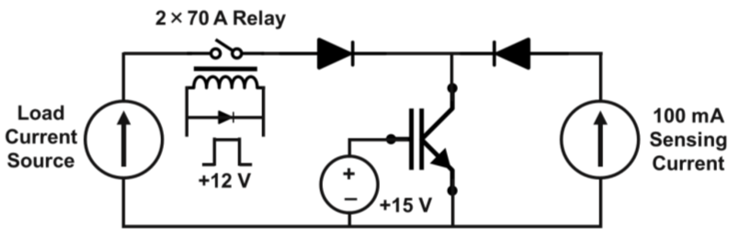
3. Power Cycling Test Setup

Figure 1 presents the primary circuit schematic for an aging experiment involving a single IGBT under examination. The test involves four IGBTs connected in a series configuration. A computer, along with an NI DAQ card, is employed to determine the heatsink temperature, while an oscilloscope acquires thermal and electrical data. A LabVIEW VISA interface manages the current and the heating-cooling process by operating the relay and defining the test’s initial parameters.
The first 200 cycles’ average is utilized to establish the IGBTs’ initial parameters, which encompass the initial voltage drop across the IGBT (VCE0) and the initial junction temperature (Tj0). A floated/isolated constant voltage source (+15 V) must be linked to the four distinct IGBT gate signals. Isolated DC-DC converters (5 V to 15 V) are implemented to supply the necessary isolated gate voltages. To measure the high-precision voltage drop across the IGBTs during the cycling process, a PicoScope® 4444 (a high-resolution differential oscilloscope), which is equipped with four differential probes, is utilized.
A widely used technique for estimating junction temperature involves measuring the VCE(sat) voltage at a low, steady sensing current, in a range of mA (usually 100 mA). This current level is chosen to ensure that the VCE(sat) value is easily measurable by an ADC and to prevent any self-heating effects in the semiconductor. In this study, we assess temperature by examining the VCE(sat), which exhibits a linear correlation with the junction temperature at lower currents. By measuring the on-state voltage VCE, the junction temperature can be indirectly determined. Notably, when the current is minimal (typically 1/1000 of the rated current), VCE’s relationship with temperature is linear [40]. The equation for the junction temperature calibration curve is as follows [40]:
V C E   ( T j ) = k i g b t T j + b i g b t
In silicon-based devices, the variable kigbt typically displays a negative temperature dependence of approximately −2 mV/°C [41]. One limitation of this approach is the low sensitivity of VCE to Tj at reduced collector currents. This necessitates accurate voltage and current measurements, which can raise the overall system cost [42]. In practical situations, this variable can only be measured when the IGBT is not in operation at high currents. As a result, it is not an ideal candidate for real-time monitoring [43].
By placing an IGBT in an oven for temperatures exceeding ambient temperature (typically ambient + 10 °C) over an adequate period, one can achieve uniform heat distribution across all its layers. Alternatively, a heated surface (e.g., hot plate) can serve the same purpose. Here, for temperatures below ambient, the IGBT has been placed in a climate chamber, with the temperature set from 10 °C to 70 °C in increments of 10 °C. Through finite element (FEM) simulations, it has been demonstrated that using a thermally conductive pad or interface material can equalize the temperature of the IGBT chip and the heated surface in just 15 s. The heated surface’s temperature is adjusted, and the procedure is performed at each temperature level. As a result, a VCE-Tj graph is generated, depicting the correlation between the IGBT junction’s temperature and the collector–emitter voltage. Four new IGBT samples were used to create the VCE-Tj graph shown in Figure 2. The near-identical nature of the curves for all samples demonstrates the high accuracy of this measurement approach and its dependency on the manufacturing quality.
In the examination technique employed, a pulsating direct current (DC), known as IH, is introduced into the device under test (DUT)—specifically, IGBTs. The purpose is to subject the DUT to power-loss pulses and related thermal fluctuations, which consist of both heating and cooling stages [44]. As the relay becomes active, the current swiftly reaches its maximum and transitions into the operating zone. The measuring current (100 mA) is constantly maintained and utilized to calculate the virtual junction temperature once the load current has been interrupted.
Upon turning off the relay, the elevated current is obstructed, allowing only the minimal sensing current to flow. Immediately after the high current is terminated, the voltage decrease across the IGBT (VCE at a low current) must be recorded, as it serves as a valuable metric for estimating the maximum junction temperature (Tjmax). Figure 3 presents a clear illustration of the method discussed.
Usually, the sensing current is introduced into the apparatus after an adequate delay (ranging up to several hundred microseconds) following the removal of the load current, ensuring that surplus carriers have been entirely cleared or recombined. As the sensing current produces minimal self-heating, it is possible to measure the voltage drop while the device cools down [45]. In the present research, the VCE at a low current will be measured 200 μs after the high current has been terminated.
This time delay is considered because the semiconductor requires a certain period to reach the essential electrical balance for the low current to pass through [46]. By projecting the temperature from the 200 μs point to the starting point, a more accurate reading can be obtained at the precise moment the current is interrupted [45]. The 200 μs delay is chosen to guarantee that electrical fluctuations have subsided and the sensing current is functioning properly. A common approach to account for this lag is to perform an extrapolation from the 200 μs point back to the initial moment (t = 0 s). For example, in a situation involving 30 A for 60 s, we conducted curve-fitting on the observed temperature values and projected the data from 200 μs back to 0 s. This extrapolation process is illustrated in Figure 4. Initially, we refined the temperature information based on the noisy measurements, ensuring the first data point was at 2 ms. The calculated junction temperature at the starting point (t = 0 s) was merely 1 °C higher than the temperature measured at 200 μs:
In the given instance, the projected junction temperature came out to be 79.78 °C as opposed to 78.64 °C (a difference of 1.14 °C) upon applying a linear regression analysis to the data points and extending the temperature from 200 μs to 0 s. While oscilloscope readings possess a satisfactory level of precision (14-bit resolution), voltage measurements tend to include some undesirable noise, which in turn impacts the recorded temperature. When dealing with longer time delays (for instance, 10 ms), it is essential to carry out a reverse extrapolation of the series of time-delayed observations to determine the accurate peak junction temperature [47].
The power cycling test setup, constructed in the laboratory of EnergyVille 2, can be seen in Figure 5.
During every power cycling evaluation, several crucial factors must be taken into account and implemented:
8.
Current: The IGBT undergoes constant thermal fluctuations at elevated currents. Typically, the current is adjusted to match the device’s specified capacity [12]. To accelerate testing, currents higher than the rated levels are occasionally used [48,49]. Nonetheless, employing values beyond the recommended range is discouraged, as accelerated conditions can lead to entirely distinct failure modes.
9.
Temperature: Operating temperature is a crucial factor in determining the duration of power cycling tests. Achieving substantial temperature fluctuations is essential for accelerating device degradation and failure while staying within the device’s specifications. Greater temperature swings have a more pronounced impact than the highest temperature [50]. The highest temperature (Tjmax) typically ranges from 100 to 150 °C [13]. The testing process employs an adjustable water-cooling mechanism for heat dissipation. Utilizing a water-cooling system allows the system’s temperature to be set lower than the surrounding environment. However, in humid conditions, condensation may form on the heatsink plate due to the cooler temperature of the heatsink lowering the air temperature nearby, consequently reducing its moisture-carrying capacity. When the air becomes oversaturated with moisture, further cooling may lead to condensation on the heatsink plate’s surface. Condensation on the heatsink plate can pose several problems, such as the potential for short circuits or damage to electronic components. To avoid these issues, the temperature of the water-cooling system should not drop below 15 °C.
10.
Cycling time: The temperature fluctuation at the junction is determined by testing a combination of the heating power, heating duration, and the thermal resistance of the device [51]. Various studies have demonstrated that distinct dominant failure mechanisms are activated within the structure depending on the length of the heating period [52,53]. From a traditional perspective, shorter cycle tests primarily affect the lifetime of bond wires, whereas longer cycles predominantly lead to failures in the solder layers [54]. The boundary between short and long cycles remains somewhat ambiguous. Some sources classify short cycles as those with heating durations under 20 s, while others consider any test with a cycle time of less than 1 min to be short. In real applications, short cycle tests typically last only a few seconds, while long cycle tests extend beyond one minute. To achieve the cooling system’s reference temperature at the end of each power cycle, the power-OFF interval (toff) is twice the length of the power-ON period (ton) [55]. Consequently, initial adjustments for power cycle tests involve setting Tjmin and Tjmax by modifying Iload, ton, toff, and the cooling to suitable levels [56]. During the test, Tjmin, Tjmax, and the resulting VCE are not further regulated, causing any increase in VCE to shift the junction temperatures. Nevertheless, VCE variability is advantageous as it mirrors actual/practical applications.
11.
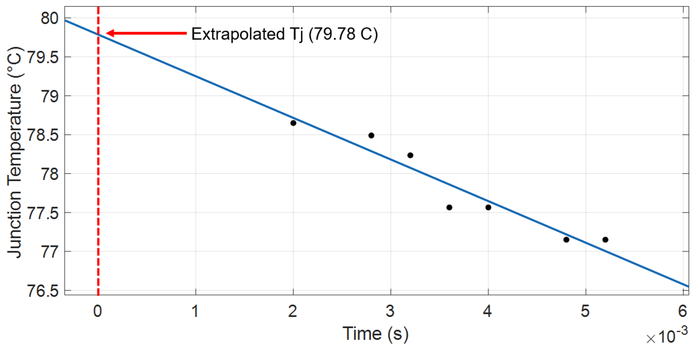
End-of-Life (EOL) benchmarks: In the majority of testing configurations, temperature and electrical data are observed throughout each cycle. If these values experience a change exceeding a predetermined threshold (for example, 20%), the EOL criteria are considered to have been met [57]. Studies have shown that a 20% increase in Rth signifies solder-fatigue failure [58]. Thermal resistance is characterized as the temperature difference between two adjacent isothermal surfaces divided by the total heat flow between them. In a power semiconductor, the junction Tj and case TC serve as the two isothermal surfaces, with Ploss representing the total heat flow between them (voltage multiplied by total current = load current + sensing current). As such, the thermal resistance can be mathematically represented as follows [28]:
R t h t = T j t T C ( t ) P l o s s ( t ) = T j t T C ( t ) V C E ( s a t ) × ( I l o a d + I s e n s e )
It is worth mentioning that accurately measuring case temperature can be difficult and necessitates adjustments to the heatsink (e.g., holes in the heatsink plate underneath the chip). Introducing a thermocouple between the IGBT case and the heatsink may result in a gap, leading to a considerable rise in IGBT temperature and diminished thermal interface efficiency. Consequently, in this research, thermal resistance measurement is not employed as an end-of-life (EOL) indicator.
The criteria for reaching EOL involve a 20% increase in forward voltage (Vf, VCE, or VDS), thermal resistance (Rth), or temperature fluctuation ΔT, each compared to their initial values [57,59]. In other research, a 5% to 20% increase in VCE(ON) has been used as an IGBT module’s EOL criterion [60], with the number of cycles leading up to these periods being tallied for a lifetime. Although this parameter is commonly used in previous studies, one investigation demonstrated that using a 5% VCE(on) increase as the EOL criterion does not accurately reflect the number of cycles to failure, as the IGBT under examination could still function for an additional 600k cycles after surpassing the 5% increase in VCE [61].
As previously discussed, we have addressed the number of cycles leading up to failure. The conversation will now shift to the development of degradation indicators, specifically VCE(sat) and Rth, throughout the power cycle test until the end-of-life signal is detected. Additionally, Tjmax can serve as a comprehensive degradation marker, since the progression of VCE(sat) and Rth significantly impacts Tjmax [62]. When the IGBT is nearing its breaking point, the anticipated ΔTj percentages fall between 10 and 16% for the three different current operation scenarios [63]. In this study, a temperature swing alteration of 20% is considered as the failure benchmark. It is important to mention that, in many tested instances, surpassing this threshold results in the IGBT exceeding its maximum allowable temperature of 175 °C after several thousand cycles, demonstrating the effectiveness of this failure standard.
Here, we subjected an IGBT to high-amplitude thermal cycles (ΔTj = 105 °C) and monitored both the collector–emitter voltage (VCE-high) at high current values and the maximum junction temperature (Tjmax) throughout the degradation process. The results, as shown in Figure 6, revealed that both parameters increased during the aging process, which is consistent with the expected degradation behavior of IGBTs.
A notable observation was the sudden increase in junction temperature and voltage at cycle 26,000, which can be attributed to bond wire failure, such as cracking or lift-off. This event marks a significant turning point in the degradation process, as bond wire failures can lead to severe performance degradation and potential device failure. Upon reaching the end-of-life point, we observed a 20% increase in the maximum junction temperature (Tjmax) and a 10.2% increase in VCE-high. The observed variation in VCE-high is in line with findings from previous studies, further validating the effectiveness of monitoring VCE as an indicator of IGBT degradation.

4. IGBT’s Lifetime Models

Power devices consist of multiple layers, each varying in thickness, materials, and physical properties. As a result, thermal expansion behaves differently for each layer when subjected to temperature changes. Over time, the thermal stress within these layers can lead to fatigue. The amplitude of temperature fluctuations (ΔTj) and the average temperature (Tjm) during thermal cycles significantly influence the lifetime of power devices. One of the most straightforward models used to describe this phenomenon is the Coffin–Manson model, which considers plastic strain as the primary cause of bond wire detachment, while elastic strain is considered negligible [64]. However, this model is only applicable when the maximum temperature stays below 120 °C and suggests a power–law relationship between the fatigue life (Nf) and temperature change (ΔT) [65]:
N f = α T j n
The values of α and n are ascertained through experimental evaluations, which can be conducted either via thermal or power cycling of actual devices. Previous research [16,66] has been dedicated to examining and assessing various life expectancy models for the reliability of power semiconductor devices. Additional exploration reveals that the mean temperature considerably influences the durability of power components, and there is a corresponding shift for varying Tjm, pointing to a thermally driven process. This influence can be incorporated into the Coffin–Manson lifetime model and articulated utilizing the Arrhenius methodology [67]:
N f = A × T j α × e x p E a k b · T j m
In this equation, Nf represents the total number of cycles before failure, while A denotes the scale parameter. The Boltzmann constant is symbolized by kb, and the activation energy is given by Ea, which is equal to 9.89 × 10⁻²⁰ joules. The constant term, represented by “a”, has a value of −5.039, and the average temperature at the junction is expressed as Tjm. These values are derived from empirical data obtained through extensive testing and analysis.
This enhanced lifetime model is commonly referred to as the modified Coffin–Manson model. It has been further developed by incorporating the frequency of thermal cycles (f) and is now known as the Norris–Landzberg model, represented by the following formula [68]:
N f = α × f n 2 × T j n 1 exp E a k b · T j m
The constants n1 and n2 are obtained from a curve fitting on the experimental cycling results. In the CIPS08 model, also known as the Bayerer model [69], several additional test parameters (such as heat on-time ton, minimum junction temperature, and current I per bond stitch) and power semiconductor design factors (like the IGBTs’ breakdown voltage V divided by 100 and the bond-wire diameter D) are considered [8,28]. By including these extra parameters, the experimental data fit, and accuracy of the durability model are substantially enhanced [27]. Equation (6) represents the CIPS08 lifetime model, which calculates the cycles to failure, Nf, based on power cycling test conditions and power semiconductor design parameters.
N f = K × T j β 1 exp β 2 T j + 273 × t o n β 3 × I β 4 × V β 5 × D β 6
In Equation (6), K is the scale factor, and the β values are determined by accurately adjusting the power cycling test outcomes, and based on Bayerer’s research, they are as follows:
  • β1 = −3.483.
  • β2 = 1917.
  • β3 = −0.438.
  • β4 = −0.717.
  • β5 = −0.751.
  • β6 = −0.564.
Similarly, the parameters for the EasyPACK IGBT module from Infineon have been obtained [70], which include the scale/technology factor K = 2.03 × 10¹⁴ and the coefficients β1 = −4.416, β2 = 1285, β3 = −0.463, β4 = −0.716, β5 = −0.761, β6 = −0.5. These findings indicate that the primary variations occur in the initial two coefficients, while the final four coefficients remain relatively consistent across various IGBT types.
Regarding active power cycling tests, the reference/absolute temperature Tj* can be represented by the highest junction temperature (Tjmax), the lowest junction temperature (Tjmin), or the average junction temperature (Tjm), defined as (Tjmin + Tjmax)/2 [71]. For a specific ∆Tj, these reference temperature values can be effortlessly converted to one another. However, this is not applicable for exponential functions, resulting in different parameter values being observed for distinct Tj* selections. All three potential choices have compelling reasons for their selection. Since the process of failure is generally hastened by elevated temperatures, it appears reasonable to utilize the maximum junction temperature (Tjmax) as a reference point, as it is more closely related to material parameters significant to the physics of failure, like the melting temperature of solder materials [71]. Conversely, the minimum junction temperature (Tjmin) demonstrates fewer connections to other factors, as thoroughly examined by the CIPS08 model [27]. Some researchers advocate for the use of the average junction temperature (Tjm) as a suitable middle ground between these two opposing limits.
The SKiM63 approach was developed based on the power cycling examination results of Semikron SKiM63 power modules containing standard silicon IGBTs and diodes [72]. This model’s mathematical expressions incorporate elements from well-established power cycle models, such as the Arrhenius equation and the Coffin–Manson principle [59]. Furthermore, it takes into account the bond wire’s aspect ratio (the proportion of loop height to the distance between bond stitches on the chip and substrate) and ton as additional influencing factors. The SKiM63 lifetime model played a pioneering role in distinguishing different failure mechanisms [62]. The primary technique for achieving this separation involves merging cutting-edge packaging methods with traditional ones. The model can be depicted as follows [73]:
N f = A × T j α × exp E a T j m k b × a r β 1 · T j + β 0 × C + t o n γ C + 1 · f d i o d e
where A is the scale factor, ar is the bond wire aspect ratio, γ is the time exponent, C is the time coefficient, and fdiode represents the effect of thickness difference of IGBT and diode on their lifetime.
It is important to mention that, for all previously discussed lifetime models, projecting the lifetime data gathered from expedited tests to actual usage situations might result in inaccurate lifetime approximations. While IGBT power modules employed in high-power applications have garnered attention in recent research, significant information voids persist concerning the reliability and lifetime projections of individual/discrete devices. Most efforts [62,74,75,76] have concentrated on the resilience of IGBT modules, which involve numerous active chips connected in parallel via multiple bond wires. A limited number of investigations have delved into the area of discrete package IGBTs [19,77,78].
According to [70], the current CIPS08 lifetime model is anticipated to forecast a lifetime nearly double that of the empirically determined lifetime. Another study [79] also discovered that the CIPS08 model’s projected lifetime is approximately 2.4 times greater than the real-world lifetime. In comparison, the LESIT lifetime model’s ratio was significantly greater, at 12 times the actual lifetime. In [68], power cycling tests were conducted on three IGBTs, all of which had the same temperature fluctuations and mean temperature, but with varying current and high-current pulse durations. The findings demonstrated that the traditional Coffin–Manson model fails to deliver accurate predictions, as the number of cycles to failure is heavily influenced by the duration of the pulses. An analysis of the actual lifetime and the projected lifetime from the CIPS08 model reveals a significant discrepancy, with the predicted lifetime being approximately 2.3 times longer than the actual one. The variance between experimental and predicted cycle counts, along with differing outcomes among various DUTs, highlights the issues with current lifetime models. One primary concern with existing models is that they are derived from accelerated aging tests on IGBT modules rather than individual-chip (discrete) IGBTs. Given the distinct packaging technologies between the two scenarios, it is reasonable to expect disparities in their lifetimes as well. Consequently, there is a need to adjust current lifetime models, especially for photovoltaic (PV) applications where discrete IGBTs are utilized.

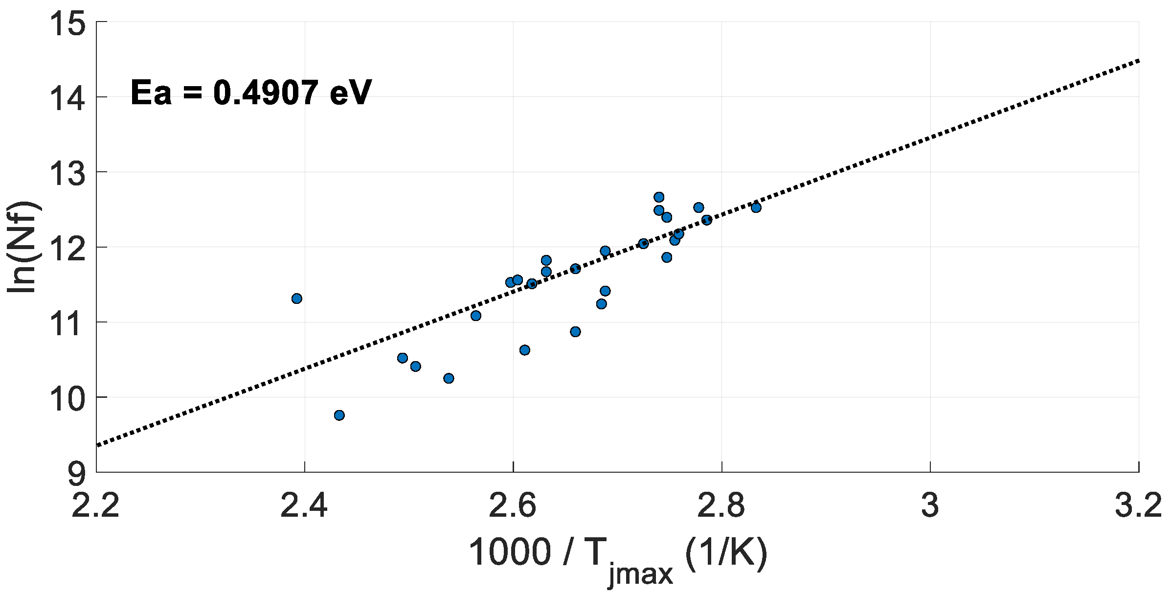
5. Results and Discussion

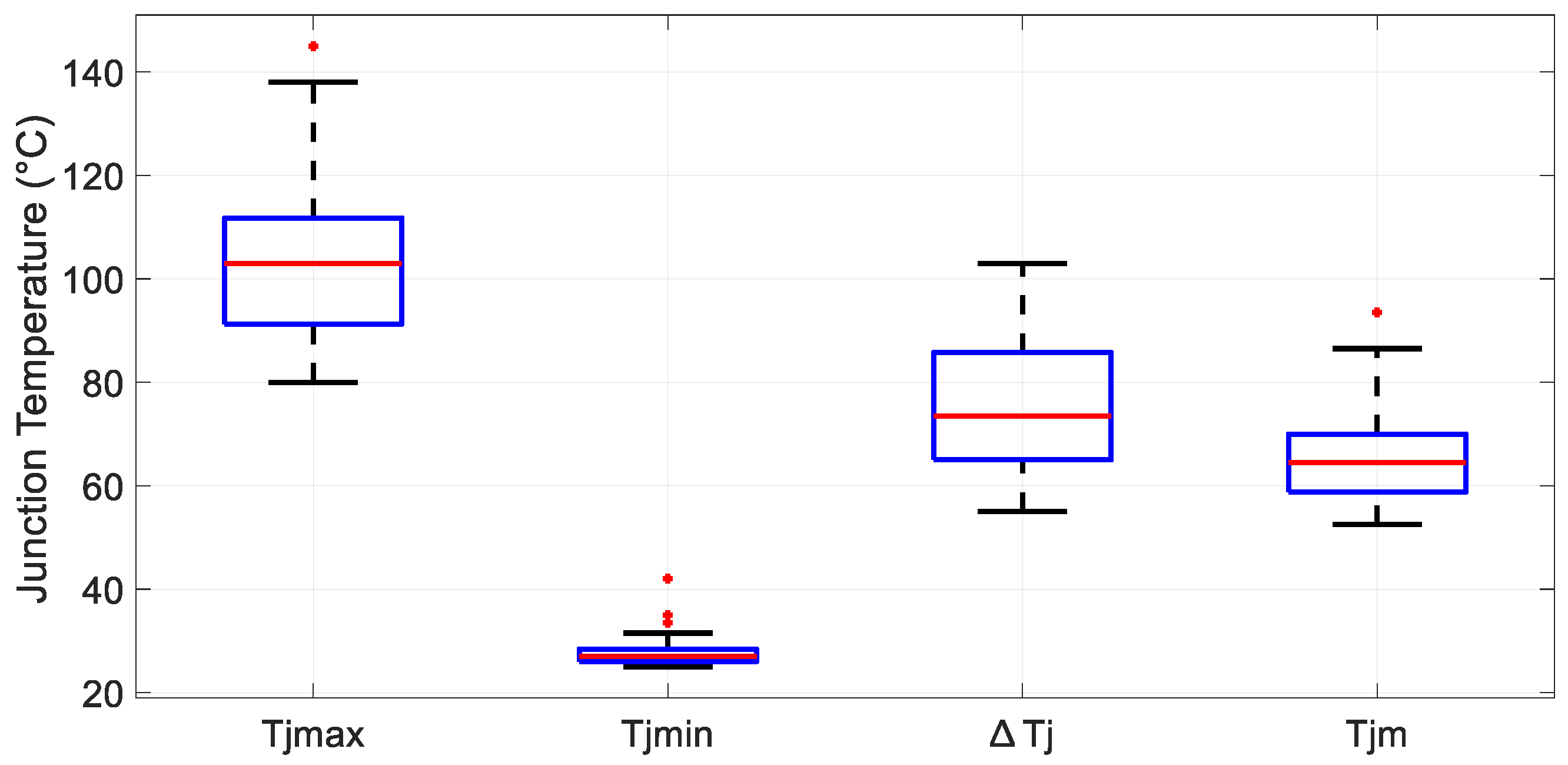
5.1. Power Cycling Results

The period of the cycle involves balancing the change in junction temperature (ΔTj) with the number of cycles that occur within a specific duration, making it challenging to identify the ideal configuration for the shortest test time. In this case, a ton = 2 s and a toff = 4 s were determined based on experience. Furthermore, the minimum and maximum junction temperatures (Tjmax) were recorded to facilitate a better understanding of the outcomes. The high current used in the experiment corresponded to the 40 A rated current, with variations in the thermal pads and fixing screw rotational force applied for distinct tests. This particular test was conducted 27 times using identical discrete IGBTs.
The maximum junction temperature (Tjmax) falls within the 80 to 145 °C range, while the minimum junction temperature (Tjmin) is typically set between 25 and 40 °C. The thermal cycle amplitude spans from 55 to 103 °C, and the mean junction temperature (Tjm) ranges from 52.5 to 93.5 °C. Figure 7 presents a box plot representation of the temperature ranges, depicting the various thermal conditions employed in the power cycling tests conducted in this study. The box plot effectively summarizes the distribution of temperature data, emphasizing the median, quartiles, and potential outliers for Tjmax, Tjmin, and Tjm.
Figure 8 and Figure 9 contain the results derived from power cycling tests on chosen Si IGBTs (FGH40T70SHD) employed in a commercial photovoltaic inverter. Figure 8 demonstrates the correlation between the amplitude of thermal cycles and the number of cycles to failure. A linear regression is fitted to this curve. By plotting Nf against 1/Tjmax, the Arrhenius dependency can be linearly represented.
Figure 10 reveals that an activation energy of 0.4907 eV has been determined based on the collected data (confidence interval = 0.0718 eV). This constant is part of the Arrhenius equation and is associated with the kinetics of the underlying physical process under thermal stress [80]. The calculated activation energy falls within the range reported in previous research (refer to [81]). The LESIT model, which focuses on Al bond wire failure in traction modules, has an activation energy of 0.808 eV, which is greater than other values extracted from existing literature. Another study [81] on Al bond wires in TO-247 packages reports an activation energy of 0.168 eV. An investigation indicated that the activation energy of the leakage current should be controlled by the diffusion mechanism. However, the temperature dependence exhibits a significant discrepancy at an activation energy close to 1.0 eV [82]. This suggests that a lower activation energy contributes to improved reliability performance.

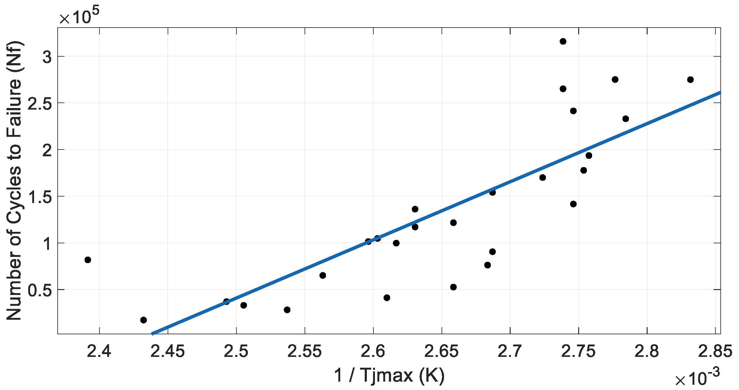
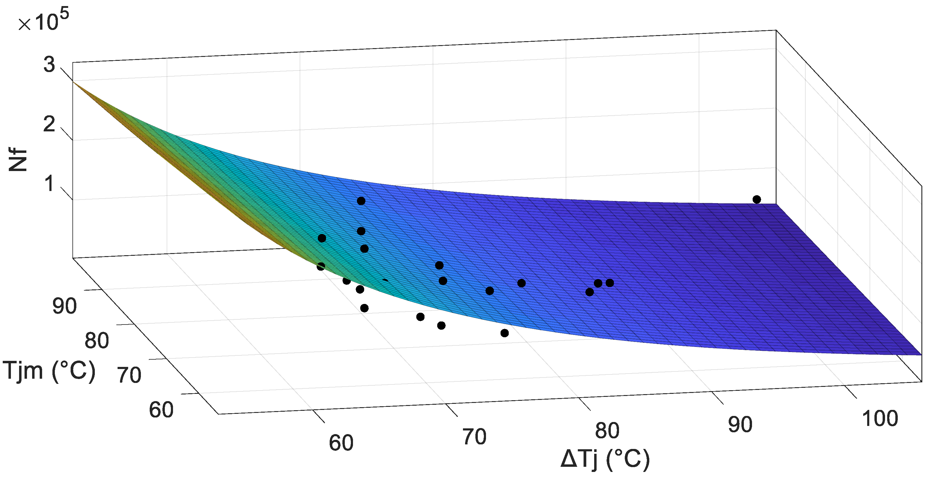
5.2. IGBT’s Modified Lifetime Models

The SKiM63 lifetime model can be adjusted based on the results obtained from the power cycling tests. Figure 11 displays the number of cycles in relation to the thermal cycle amplitude (ΔTj) for both the actual experiments and the SKiM63 model. A linear curve can be fitted to the data points derived from actual power cycling. One method that can be used to alter this lifetime model is to introduce an additional/modification exponential index that depends on ΔTj. Thus, the revised lifetime model will be as follows:
N f = i n d e x A × T j α × exp E a T j m a x k b × a r β 1 · T j + β 0 × C + t o n γ C + 1 · f d i o d e
where the index is
i n d e x = a exp b T j   a = 0.1777 b = 0.1233
An alternative approach involves fitting the entire equation to the curve and determining the adjusted coefficients. The activation energy acquired from the previous stage (0.4425 eV) is incorporated into the SKiM63 formula. The Coffin–Manson factor (α) characterizes the influence of the temperature fluctuation ΔTj. An Arrhenius expression illustrates the lifetime’s reliance on the average junction temperature Tjm. For IGBTs with a blocking voltage below 1200 V, the factor fdiode is set to one [59]. The parameter ar indicates the dependency on the wire bond aspect ratio. The bond wire loop ratio, derived (0.177) from the IGBT’s X-ray images, is shown in Figure 12.
The findings of the study indicated that the number of cycles until heel crack failure is significantly influenced by the shape of the loop. When the loop’s height-to-width ratio shifts from 0.2 to 0.3, there is a tenfold increase in the number of cycles to failure [83]. As the aspect ratios of wire bonds grow, the failure modes shift from solely heel cracking to complete lift-off. It becomes clear that for aspect ratios under 0.3, the wire bond is the sole constraint on the module’s power cycling capacity [84]. The coefficients C and γ demonstrate a reliance on the duration of the load pulse (ton) and are derived from assumptions about temperature gradients and plastic deformation [73]. Table 1 presents a comparison between the modified coefficients and the conventional coefficients for the SKiM63 lifetime model. The curve fitting’s measured R2 and RMSE values were found to be 0.732 and 43,921, respectively. The narrow confidence bounds achieved indicate that the fitted curve is satisfactory and does not deviate significantly from the expected results. The observed variations in the lifetime model coefficients indicate that the selected discrete IGBT exhibits distinct failure and lifetime behavior compared to the IGBT module packages used to estimate the conventional model coefficients.
As shown, the scale factor in our instance is much smaller compared to the conventional case. The Coffin–Manson factor (α) is also somewhat lower than that of the conventional fitted model. The reduced ar factor likely indicates enhanced reliability performance for the bond wires, where cracks pose the primary concern for the IGBT. In this scenario, the adjusted coefficients β1 and β0 underwent significant alterations. The coefficient β1 decreased by a factor of 10, whereas the coefficient β0 experienced an approximately tenfold increase.
The parameter γ (time exponent) pertains to the pulse duration. In the prior fitted model, this parameter is normalized to a pulse duration of 1 s and increases as the pulse duration decreases. In this instance, since we only conducted power cycling tests with an on-time of 2 s, it was challenging to incorporate the impact of switching time on the device’s lifetime. Consequently, the coefficients C (time coefficient) and γ, associated with the cycling periods, were held constant at the values derived from the conventional method.
The CIPS08 model is a more general and versatile model for power cycling lifetime estimation of IGBTs compared to the SKiM63 model, which is specific to the SKiM family of IGBT modules. Hence, fitting power cycling experimental data on the CIPS08 model can provide more meaningful insights into the lifetime of IGBT. The subsequent step involves applying the CIPS08 model to the acquired cycling data to adjust the model’s coefficients. With two bond stitches, the current per bond amounts to 20 A. The specified voltage for the IGBT under consideration is 700 V, resulting in a V value (rated voltage divided by 100) of 7. Upon physical examination, the bond wire diameter has been determined to be 220 μm. Additionally, the on-time for the thermal cycles is set at 2 s. To streamline the curve-fitting process, these constant parameters β4–β6 are integrated into the scale coefficient (K). In previous studies, the four coefficients β1–β4 associated with these parameters exhibit minimal variation among different IGBT types. After applying the CIPS08 model to the data, the coefficients are calculated as listed in Table 2.
Figure 13 shows the CIPS08 model equation fitted to the experimental cycling data. The curve fitting yields an R2 value of 0.741 and an RMSE of 43,148, indicating a reasonable level of accuracy at low temperatures. The coefficients were derived using the least square method, along with their confidence bounds, as listed in Table 2. In the case of curve fitting, we observed exceptionally high (95%) confidence bounds for the estimated coefficients, which suggests a significant level of uncertainty in the parameter estimates. Various factors could contribute to these high confidence bounds. For instance, having too few data points or insufficient data might prevent the algorithm from properly estimating the parameters, resulting in increased uncertainty. Another potential cause could be the selection of the model-based equation. If the chosen model fails to accurately capture the underlying relationship between the variables, the curve-fitting algorithm may have difficulty finding an appropriate fit, leading to greater uncertainty in the estimated parameters. Nonetheless, as observed in Table 1 and Table 2, the confidence bounds are not substantially greater than the estimated values. This demonstrates that the curve fitting is acceptable, and there are no overfitting concerns in our analysis.

5.3. Example of the Modified Lifetime Models

In the considered case study, we examine the impact of lifetime modifications on the predicted lifetime of PV inverters using a mission/load profile, as illustrated in Figure 14. Since the power cycling test has limited data points, it is preferable to apply a modification index to align the SKiM63 or CIPS08 models with the available power cycling test results. This is because these lifetime models have been adjusted based on a larger set of measurements. Additionally, a 5% uncertainty is incorporated in the Monte Carlo simulation to account for 95% confidence bounds. Figure 15 shows the unreliability function before and after the SKiM lifetime modification using the proposed index. The adjusted lifetime prediction is notably more accurate, falling within the expected actual lifetime range of PV inverters. In contrast, the unmodified lifetime model could overestimate the lifespan by up to 44 years.
The B10 lifetimes for the modified and unmodified models are 13.56 and 43.79 years, respectively. The B1 lifetime, in which 1% of the total population would fail, also demonstrates a significant discrepancy between the unmodified (24.49 years) and modified (7.53 years) models.
Another limitation of our modified fitted parameters is that the power cycling tests were conducted solely for a single on-time value (ton = 2 s), rendering it impossible to determine the PV inverter’s life consumption at a grid frequency of 50 Hz. Nonetheless, our model effectively captures the long-term mission profile effects. For instance, by employing the SKiM63 lifetime model, we can calculate the long-term life consumption for the PV inverter. When focusing solely on the long-term life consumption (with a 15 min time-step) and disregarding the 50 Hz life consumption, the estimated lifetime becomes significantly larger (1377.78 years). However, utilizing the modified lifetime model results in a much more realistic predicted lifetime (18.68 years). The calculated coefficients, along with their corresponding confidence bounds, can be integrated into Monte Carlo simulations as an alternative to assuming a 5% random uncertainty. This approach provides a more accurate representation of the uncertainties involved.

6. Conclusions

This study aimed to enhance the accuracy and reliability of lifetime prediction models for IGBTs by refining and validating two prominent models: the CIPS08 and SKiM63 models. Through comprehensive experimental power cycling tests, we calibrated these models to better reflect the specific operational conditions and degradation patterns encountered in different IGBT types and applications, particularly focusing on high-stress environments such as photovoltaic (PV) inverters. The research involved extensive power cycling tests designed to simulate real-world operational stresses on discrete IGBTs. These tests subjected IGBTs to high-amplitude thermal cycles (ΔTj = 105 °C) and monitored key parameters like the collector–emitter voltage (VCE-high) at high current values and the maximum junction temperature (Tjmax) throughout the degradation process. The experimental setup utilized a series configuration of four IGBTs, with data acquisition managed via an NI DAQ card and an oscilloscope, controlled through a LabVIEW VISA interface. Key parameters such as the load current, gate voltage, and pulse duration were meticulously controlled, ensuring accurate and repeatable results.
The results from the power cycling tests revealed significant increases in both Tjmax and VCE-high during the aging process, consistent with expected degradation behaviors. A notable observation was the sudden increase in junction temperature and voltage at the last thousand cycles, showing the bond wire failures such as cracking or lift-off. This event marked a critical point in the degradation process, highlighting the importance of monitoring these parameters. Upon reaching the end-of-life point, a 20% increase in Tjmax and a 10.2% increase in VCE-high were recorded. These observations align with previous studies, validating the use of VCE and Tjmax as reliable indicators of IGBT degradation.
By integrating these empirical data, the CIPS08 and SKiM63 models have been recalibrated. For the CIPS08 model, the coefficients were adjusted as follows: β1 = −2.910, β2 = 1083.714, and β3 = −4.521. This recalibration improved the model’s accuracy, evidenced by an R2 value of 0.741 and a reduced RMSE of 43,148. Similarly, for the SKiM63 model, an additional exponential index dependent on ΔTj was introduced, with derived parameters a = 0.1777 and b = −0.1233, further enhancing its fit to the experimental data. As an example, the recalibrated models demonstrated a significant reduction in B10 lifetimes from 43 years in the unmodified model to 13 years in the modified model, underscoring the critical need for ongoing modification and validation based on operational data. The refined models have the potential to greatly impact the design and maintenance strategies of power electronic systems, enhancing the reliability of these systems.
Future work should aim to further refine these models by incorporating larger datasets, exploring the effects of new IGBT technologies, and extending the models’ applicability to other types of semiconductor devices. Additionally, as the field progresses, the integration of machine learning techniques could offer new insights and predictive capabilities, and further possibilities for enhancing the reliability and efficiency of power electronic systems.

Author Contributions

Conceptualization, O.A., W.D.C. and M.D.; methodology, O.A.; software, O.A.; validation, O.A. and M.D.; formal analysis, O.A.; investigation, O.A.; resources, W.D.C. and M.D.; data curation, O.A.; writing—original draft preparation, O.A.; writing—review and editing, W.D.C. and M.D; visualization, O.A.; supervision, W.D.C. and M.D.; project administration, M.D.; funding acquisition, M.D. All authors have read and agreed to the published version of the manuscript.

Funding

This work has been supported by Flanders Innovation and Entrepreneurship and Flux50 under project DAPPER, HBC.2020.2144.

Data Availability Statement

Data supporting this study are included within the article.

Conflicts of Interest

The authors declare no conflicts of interest.

References

  1. Li, C.; Li, Y.S.; Liu, J.X.; Shao, H.Q.; yuan Chen, Z.; Li, J.Y. Research on performance parameter degradation of high voltage and high power IGBT module in power cycling test. J. Phys. Conf. Ser. 2022, 2290, 012041. [Google Scholar] [CrossRef]
  2. Tounsi, M.; Oukaour, A.; Tala-Ighil, B.; Gualous, H.; Boudart, B.; Aissani, D. Characterization of high-voltage IGBT module degradations under PWM power cycling test at high ambient temperature. Microelectron. Reliab. 2010, 50, 1810–1814. [Google Scholar] [CrossRef]
  3. Ali, S.H.; Ugur, E.; Akin, B. Analysis of Vth variations in IGBTs under thermal stress for improved condition monitoring in automotive power conversion systems. IEEE Trans. Veh. Technol. 2018, 68, 193–202. [Google Scholar] [CrossRef]
  4. Anderson, J.M.; Cox, R.W. On-line condition monitoring for MOSFET and IGBT switches in digitally controlled drives. In Proceedings of the 2011 IEEE Energy Conversion Congress and Exposition, Phoenix, AZ, USA, 17–22 September 2011; pp. 3920–3927. [Google Scholar]
  5. Moeini, R.; Tricoli, P.; Hemida, H.; Baniotopoulos, C. Increasing the reliability of wind turbines using condition monitoring of semiconductor devices: A review. IET Renew. Power Gener. 2018, 12, 182–189. [Google Scholar] [CrossRef]
  6. Halick, M.S.M.; Kandasamy, K.; Jet, T.K.; Sundarajan, P. Online computation of IGBT on-state resistance for off-shelf three-phase two-level power converter systems. Microelectron. Reliab. 2016, 64, 379–386. [Google Scholar] [CrossRef]
  7. Frank, Ø.B. Power Cycle Testing of Press-Pack IGBT Chips. Master’s Thesis, NTNU, Trondheim, Norway, 2014. [Google Scholar]
  8. Patil, N.; Das, D.; Goebel, K.; Pecht, M. Identification of failure precursor parameters for insulated gate bipolar transistors (IGBTs). In Proceedings of the 2008 International Conference on Prognostics and Health Management, Denver, CO, USA, 6–9 October 2008; pp. 1–5. [Google Scholar]
  9. Wang, B.; Cai, J.; Du, X.; Zhou, L. Review of power semiconductor device reliability for power converters. CPSS Trans. Power Electron. Appl. 2017, 2, 101–117. [Google Scholar] [CrossRef]
  10. Zhang, Y.; Liu, Y.; Li, C.; Li, J. Analysis of fault precursor parameters under accelerated aging tests for IGBT modules. In Proceedings of the 2020 17th China International Forum on Solid State Lighting & 2020 International Forum on Wide Bandgap Semiconductors China (SSLChina: IFWS), Shenzhen, China, 23–25 November 2020; pp. 238–241. [Google Scholar]
  11. Hu, Z.; Ge, X.; Xie, D.; Zhang, Y.; Yao, B.; Dai, J.; Yang, F. An aging-degree evaluation method for IGBT bond wire with online multivariate monitoring. Energies 2019, 12, 3962. [Google Scholar] [CrossRef]
  12. GopiReddy, L.R.; Tolbert, L.M.; Ozpineci, B. Power cycle testing of power switches: A literature survey. IEEE Trans. Power Electron. 2014, 30, 2465–2473. [Google Scholar]
  13. Smet, V.; Forest, F.; Huselstein, J.-J.; Richardeau, F.; Khatir, Z.; Lefebvre, S.; Berkani, M. Ageing and failure modes of IGBT modules in high-temperature power cycling. IEEE Trans. Ind. Electron. 2011, 58, 4931–4941. [Google Scholar] [CrossRef]
  14. Gao, B.; Yang, F.; Chen, M.; Chen, Y.; Lai, W.; Liu, C. Thermal lifetime estimation method of IGBT module considering solder fatigue damage feedback loop. Microelectron. Reliab. 2018, 82, 51–61. [Google Scholar] [CrossRef]
  15. Wang, F.; Yang, Y.; Huang, T.; Xu, Y. Lifetime prediction of electronic devices based on the P-stacking machine learning model. Microelectron. Reliab. 2023, 146, 115027. [Google Scholar] [CrossRef]
  16. Zhang, Y.; Wang, H.; Wang, Z.; Yang, Y.; Blaabjerg, F. Impact of lifetime model selections on the reliability prediction of IGBT modules in modular multilevel converters. In Proceedings of the 2017 IEEE Energy Conversion Congress and Exposition (ECCE), Cincinnati, OH, USA, 1–5 October 2017; pp. 4202–4207. [Google Scholar]
  17. Huang, H.; Mawby, P.A. A lifetime estimation technique for voltage source inverters. IEEE Trans. Power Electron. 2012, 28, 4113–4119. [Google Scholar] [CrossRef]
  18. Choi, U.-M.; Ma, K.; Blaabjerg, F. Validation of lifetime prediction of IGBT modules based on linear damage accumulation by means of superimposed power cycling tests. IEEE Trans. Ind. Electron. 2017, 65, 3520–3529. [Google Scholar] [CrossRef]
  19. Ali, S.H.; Heydarzadeh, M.; Dusmez, S.; Li, X.; Kamath, A.S.; Akin, B. Lifetime estimation of discrete IGBT devices based on Gaussian process. IEEE Trans. Ind. Appl. 2017, 54, 395–403. [Google Scholar] [CrossRef]
  20. Ismail, A.; Saidi, L.; Sayadi, M.; Benbouzid, M. Remaining useful lifetime prediction of thermally aged power insulated gate bipolar transistor based on Gaussian process regression. Trans. Inst. Meas. Control 2020, 42, 2507–2518. [Google Scholar] [CrossRef]
  21. Moniruzzaman, M.; Okilly, A.H.; Choi, S.; Baek, J.; Mannan, T.I.; Islam, Z. A Comprehensive Study of Machine Learning Algorithms for GPU based Real-time Monitoring and Lifetime Prediction of IGBTs. In Proceedings of the 2024 IEEE Applied Power Electronics Conference and Exposition (APEC), Long Beach, CA, USA, 25–29 February 2024; pp. 2678–2684. [Google Scholar]
  22. Qin, F.; Bie, X.; An, T.; Dai, J.; Dai, Y.; Chen, P. A lifetime prediction method for IGBT modules considering the self-accelerating effect of bond wire damage. IEEE J. Emerg. Sel. Top. Power Electron. 2020, 9, 2271–2284. [Google Scholar] [CrossRef]
  23. Li, L.-L.; Liu, Z.-F.; Tseng, M.-L.; Zhou, L.; Qi, F.-D. Prediction of IGBT power module remaining lifetime using the aging state approach. Microelectron. Reliab. 2019, 102, 113476. [Google Scholar] [CrossRef]
  24. Li, W.; Wang, B.; Liu, J.; Zhang, G.; Wang, J. IGBT aging monitoring and remaining lifetime prediction based on long short-term memory (LSTM) networks. Microelectron. Reliab. 2020, 114, 113902. [Google Scholar] [CrossRef]
  25. Zhang, J.; Hu, J.; You, H.; Jia, R.; Wang, X.; Zhang, X. A remaining useful life prediction method of IGBT based on online status data. Microelectron. Reliab. 2021, 121, 114124. [Google Scholar] [CrossRef]
  26. Li, L.; He, Y.; Wang, L.; Wang, C.; Liu, X. IGBT lifetime model considering composite failure modes. Mater. Sci. Semicond. Process. 2022, 143, 106529. [Google Scholar] [CrossRef]
  27. Bayerer, R.; Herrmann, T.; Licht, T.; Lutz, J.; Feller, M. Model for power cycling lifetime of IGBT modules-various factors influencing lifetime. In Proceedings of the 5th International Conference on Integrated Power Electronics Systems, Nuremberg, Germany, 11–13 March 2008; pp. 1–6. [Google Scholar]
  28. Sathik, M.H.M.; Sundararajan, P.; Sasongko, F.; Pou, J.; Natarajan, S. Comparative analysis of IGBT parameters variation under different accelerated aging tests. IEEE Trans. Electron Devices 2020, 67, 1098–1105. [Google Scholar] [CrossRef]
  29. Rashed, A.; Forest, F.; Huselstein, J.-J.; Martire, T.; Enrici, P. On-line [TJ, Vce] monitoring of IGBTs stressed by fast power cycling tests. In Proceedings of the 2013 15th European Conference on Power Electronics and Applications (EPE), Lille, France, 2–6 September 2013; pp. 1–9. [Google Scholar]
  30. Scheuermann, U.; Junghaenel, M. Limitation of power module lifetime derived from active power cycling tests. In Proceedings of the CIPS 2018: 10th International Conference on Integrated Power Electronics Systems, Stuttgart, Germany, 20–22 March 2018; pp. 1–10. [Google Scholar]
  31. Ghimire, P.; Pedersen, K.B.; Rannestad, B.; Munk-Nielsen, S. Ageing monitoring in IGBT module under sinusoidal loading. Microelectron. Reliab. 2015, 55, 1945–1949. [Google Scholar] [CrossRef]
  32. Choi, U.; Blaabjerg, F.; Iannuzzo, F. Advanced power cycler with intelligent monitoring strategy of IGBT module under test. Microelectron. Reliab. 2017, 76, 522–526. [Google Scholar] [CrossRef]
  33. Jia, Y.; Huang, Y.; Xiao, F.; Deng, H.; Duan, Y.; Iannuzzo, F. Impact of solder degradation on V CE of IGBT module: Experiments and modeling. IEEE J. Emerg. Sel. Top. Power Electron. 2019, 10, 4536–4545. [Google Scholar] [CrossRef]
  34. Saha, S.; Celaya, J.R.; Vashchenko, V.; Mahiuddin, S.; Goebel, K.F. Accelerated aging with electrical overstress and prognostics for power MOSFETs. In Proceedings of the IEEE 2011 EnergyTech, Cleveland, OH, USA, 25–26 May 2011; pp. 1–6. [Google Scholar]
  35. Marrakh, R.; Bouhdada, A. Modeling of interface defect distribution for an n-mosfets under hot-carrier stressing. Act. Passiv. Electron. Compon. 2000, 23, 137–144. [Google Scholar] [CrossRef]
  36. Zeng, G.; Cao, H.; Chen, W.; Lutz, J. Difference in device temperature determination using pn-junction forward voltage and gate threshold voltage. IEEE Trans. Power Electron. 2018, 34, 2781–2793. [Google Scholar] [CrossRef]
  37. Blackburn, D.L. Temperature measurements of semiconductor devices—A review. In Proceedings of the Twentieth Annual IEEE Semiconductor Thermal Measurement and Management Symposium (IEEE Cat. No. 04CH37545), San Jose, CA, USA, 11–12 March 2004; pp. 70–80. [Google Scholar]
  38. Eleffendi, M.A.; Johnson, C.M. Evaluation of on-state voltage V CE (ON) and threshold voltage Vth for real-time health monitoring of IGBT power modules. In Proceedings of the 2015 17th European Conference on Power Electronics and Applications (EPE’15 ECCE-Europe), Geneva, Switzerland, 8–10 September 2015; pp. 1–10. [Google Scholar]
  39. Avenas, Y.; Dupont, L.; Khatir, Z. Temperature measurement of power semiconductor devices by thermo-sensitive electrical parameters—A review. IEEE Trans. Power Electron. 2011, 27, 3081–3092. [Google Scholar] [CrossRef]
  40. Zhu, Y.; Xiao, M.; Su, X.; Lu, K.; Wu, Z.; Yang, G. IGBT junction temperature measurement under active-short-circuit and locked-rotor modes in new energy vehicles. IEEE Access 2020, 8, 114401–114412. [Google Scholar] [CrossRef]
  41. Baker, N.; Munk-Nielsen, S.; Iannuzzo, F.; Liserre, M. IGBT junction temperature measurement via peak gate current. IEEE Trans. Power Electron. 2015, 31, 3784–3793. [Google Scholar] [CrossRef]
  42. Arya, A.; Chanekar, A.; Deshmukh, P.; Verma, A.; Anand, S. Accurate online junction temperature estimation of IGBT using inflection point based updated I–V characteristics. IEEE Trans. Power Electron. 2021, 36, 9826–9836. [Google Scholar] [CrossRef]
  43. Qiu, X.; Zhang, G.; Chen, W.; Yu, T.; Hou, X.; Zhang, Q.; Xu, G. Review of igbt junction temperature extraction and estimation methods. IOP Conf. Ser. Mater. Sci. Eng. 2020, 774, 012091. [Google Scholar] [CrossRef]
  44. Zhu, Y.; Ma, K.; Cai, X. Thermal characterization method of power semiconductors based on H-bridge testing circuit. IEEE Trans. Power Electron. 2019, 34, 8268–8273. [Google Scholar] [CrossRef]
  45. Baker, N.; Dupont, L.; Munk-Nielsen, S.; Iannuzzo, F.; Liserre, M. IR camera validation of IGBT junction temperature measurement via peak gate current. IEEE Trans. Power Electron. 2016, 32, 3099–3111. [Google Scholar] [CrossRef]
  46. Amoiridis, A.; Anurag, A.; Ghimire, P.; Munk-Nielsen, S.; Baker, N. Vce-based chip temperature estimation methods for high power IGBT modules during power cycling—A comparison. In Proceedings of the 2015 17th European Conference on Power Electronics and Applications (EPE’15 ECCE-Europe), Geneva, Switzerland, 8–10 September 2015; pp. 1–9. [Google Scholar]
  47. Sleszynski, W.; Nieznanski, J.; Cichowski, A.; Luszcz, J.; Wojewodka, A. Evaluation of selected diagnostic variables for the purpose of assessing the ageing effects in high-power IGBTs. In Proceedings of the 2010 IEEE International Symposium on Industrial Electronics, Bari, Italy, 4–7 July 2010; pp. 821–825. [Google Scholar]
  48. Wei, L.; Kerkman, R.J.; Lukaszewski, R.A. Evaluation of power semiconductors power cycling capabilities for adjustable speed drive. In Proceedings of the 2008 IEEE Industry Applications Society Annual Meeting, Edmonton, AB, Canada, 5–9 October 2008; pp. 1–10. [Google Scholar]
  49. Wei, L.; Lukaszewski, R.A.; Lipo, T.A. Analysis of power cycling capability of IGBT modules in a conventional matrix converter. In Proceedings of the 2008 IEEE Industry Applications Society Annual Meeting, Edmonton, AB, Canada, 5–9 October 2008; pp. 1–8. [Google Scholar]
  50. Sankaran, V.; Chen, C.; Avant, C.; Xu, X. Power cycling reliability of IGBT power modules. In Proceedings of the IAS’97. Conference Record of the 1997 IEEE Industry Applications Conference Thirty-Second IAS Annual Meeting, New Orleans, LA, USA, 5–9 October 1997; pp. 1222–1227. [Google Scholar]
  51. Sarkany, Z.; Vass-Varnai, A.; Rencz, M. Effect of power cycling parameters on predicted IGBT lifetime. In Proceedings of the 2015 IEEE Aerospace Conference, Big Sky, MT, USA, 7–14 March 2015; pp. 1–9. [Google Scholar]
  52. Amro, R.; Lutz, J.; Rudzki, J.; Thoben, M.; Lindemann, A. Double-sided low-temperature joining technique for power cycling capability at high temperature. In Proceedings of the 2005 European Conference on Power Electronics and Applications, Dresden, Germany, 11–14 September 2005; p. 10-pp. [Google Scholar]
  53. Herrmann, T.; Feller, M.; Lutz, J.; Bayerer, R.; Licht, T. Power cycling induced failure mechanisms in solder layers. In Proceedings of the 2007 European Conference on Power Electronics and Applications, Aalborg, Denmark, 2–5 September 2007; pp. 1–7. [Google Scholar]
  54. Wu, W.; Held, M.; Jacob, P.; Scacco, P.; Birolini, A. Investigation on the long term reliability of power IGBT modules. In Proceedings of the International Symposium on Power Semiconductor Devices and IC’s: ISPSD’95, Yokohama, Japan, 23–25 May 1995; pp. 443–448. [Google Scholar]
  55. Tran, S.-H.; Khatir, Z.; Lallemand, R.; Ibrahim, A.; Ousten, J.-P.; Ewanchuk, J.; Mollov, S.V. Constant Δtj power cycling strategy in DC mode for top-metal and bond-wire contacts degradation investigations. IEEE Trans. Power Electron. 2018, 34, 2171–2180. [Google Scholar] [CrossRef]
  56. Held, M.; Jacob, P.; Nicoletti, G.; Scacco, P.; Poech, M.-H. Fast power cycling test of IGBT modules in traction application. In Proceedings of the Second International Conference on Power Electronics and Drive Systems, Singapore, 26–29 May 1997; pp. 425–430. [Google Scholar]
  57. Hutzler, A.; Zeyss, F.; Vater, S.; Tokarski, A.; Schletz, A.; März, M. Power Cycling Community 1995–2014. Bodo’s Power Syst. 2014, 2014, 78–80. [Google Scholar]
  58. Scheuermann, U.; Hecht, U. Power cycling lifetime of advanced power modules for different temperature swings. PCIM Nuremberg 2002, 5964, 2201–2207. [Google Scholar]
  59. Wintrich, A. Power Cycle Model for IGBT Product Lines; SEMIKRON Application Note AN 21-001; SEMIKRON: Nuremberg, Germany, 2021. [Google Scholar]
  60. Choi, U.; Jørgensen, S.; Iannuzzo, F.; Blaabjerg, F. Power cycling test of transfer molded IGBT modules by advanced power cycler under different junction temperature swings. Microelectron. Reliab. 2018, 88, 788–794. [Google Scholar] [CrossRef]
  61. Zhang, Y.; Wu, R.; Iannuzzo, F.; Wang, H. Aging investigation of the latest standard dual power modules using improved interconnect technologies by power cycling test. Microelectron. Reliab. 2022, 138, 114740. [Google Scholar] [CrossRef]
  62. Abuelnaga, A.; Narimani, M.; Bahman, A.S. A review on IGBT module failure modes and lifetime testing. IEEE Access 2021, 9, 9643–9663. [Google Scholar] [CrossRef]
  63. Tian, B.; Qiao, W.; Wang, Z.; Gachovska, T.; Hudgins, J.L. Monitoring IGBT’s health condition via junction temperature variations. In Proceedings of the 2014 IEEE Applied Power Electronics Conference and Exposition-APEC 2014, Fort Worth, TX, USA, 16–20 March 2014; pp. 2550–2555. [Google Scholar]
  64. Riedel, G.; Schmidt, R.; Liu, C.; Beyer, H.; Alaperae, I. Reliability of large area solder joints within IGBT modules: Numerical modeling and experimental results. In Proceedings of the 2012 7th International Conference on Integrated Power Electronics Systems (CIPS), Nuremberg, Germany, 6–8 March 2012; pp. 1–6. [Google Scholar]
  65. Ciappa, M. Selected failure mechanisms of modern power modules. Microelectron. Reliab. 2002, 42, 653–667. [Google Scholar] [CrossRef]
  66. Busca, C.; Teodorescu, R.; Blaabjerg, F.; Munk-Nielsen, S.; Helle, L.; Abeyasekera, T.; Rodríguez, P. An overview of the reliability prediction related aspects of high power IGBTs in wind power applications. Microelectron. Reliab. 2011, 51, 1903–1907. [Google Scholar] [CrossRef]
  67. Alhmoud, L. Reliability improvement for a high-power IGBT in wind energy applications. IEEE Trans. Ind. Electron. 2018, 65, 7129–7137. [Google Scholar] [CrossRef]
  68. Kovačević, I.; Drofenik, U.; Kolar, J.W. New physical model for lifetime estimation of power modules. In Proceedings of the 2010 International Power Electronics Conference-ECCE ASIA, Sapporo, Japan, 21–24 June 2010; pp. 2106–2114. [Google Scholar]
  69. Lutz, J. Packaging and reliability of power modules. In Proceedings of the CIPS 2014: 8th International Conference on Integrated Power Electronics Systems, Nuremberg, Germany, 25–27 February 2014; pp. 1–8. [Google Scholar]
  70. Böttcher, M.; Paulsen, M.; Fuchs, F.W. Laboratory setup for power cycling of igbt modules with monitoring of on-state voltage and thermal resistance for state of aging detection. In Proceedings of the Conference Records PCIM 2012, Nuremberg, Germany, 8–10 May 2012. [Google Scholar]
  71. Schmidt, R.; Zeyss, F.; Scheuermann, U. Impact of absolute junction temperature on power cycling lifetime. In Proceedings of the 2013 15th European Conference on Power Electronics and Applications (EPE), Lille, France, 2–6 September 2013; pp. 1–10. [Google Scholar]
  72. Hoffmann, F.; Kaminski, N. Power cycling capability and lifetime estimation of discrete silicon carbide power devices. Mater. Sci. Forum 2020, 1004, 977–984. [Google Scholar] [CrossRef]
  73. Scheuermann, U.; Schmidt, R. Impact of load pulse duration on power cycling lifetime of Al wire bonds. Microelectron. Reliab. 2013, 53, 1687–1691. [Google Scholar] [CrossRef]
  74. Deng, E.; Zhang, J.; Zhao, Z.; Chen, J.; Li, J.; Huang, Y. Influence of the clamping force on the power cycling lifetime reliability of press pack IGBT sub-module. J. Eng. 2019, 2019, 2435–2439. [Google Scholar] [CrossRef]
  75. Feller, L.; Hartmann, S.; Schneider, D. Lifetime analysis of solder joints in high power IGBT modules for increasing the reliability for operation at 150 C. Microelectron. Reliab. 2008, 48, 1161–1166. [Google Scholar] [CrossRef]
  76. Choi, U.; Vernica, I.; Zhou, D.; Blaabjerg, F. Comparative evaluation of reliability assessment methods of power modules in motor drive inverter. Microelectron. Reliab. 2020, 114, 113730. [Google Scholar] [CrossRef]
  77. Dusmez, S.; Ali, S.H.; Heydarzadeh, M.; Kamath, A.S.; Duran, H.; Akin, B. Aging precursor identification and lifetime estimation for thermally aged discrete package silicon power switches. IEEE Trans. Ind. Appl. 2016, 53, 251–260. [Google Scholar] [CrossRef]
  78. Patil, N.; Celaya, J.; Das, D.; Goebel, K.; Pecht, M. Precursor parameter identification for insulated gate bipolar transistor (IGBT) prognostics. IEEE Trans. Reliab. 2009, 58, 271–276. [Google Scholar] [CrossRef]
  79. Yangjie, B.; Jiang, Q. Summary of Life Prediction and Failure Analysis of IGBT Modules Based on Accelerated Aging Test. In Proceedings of the 2019 22nd International Conference on Electrical Machines and Systems (ICEMS), Harbin, China, 11–14 August 2019; pp. 1–5. [Google Scholar]
  80. Chamund, D.; Newcombe, D. IGBT Module Reliability; Application Note AN5945-6; Dynex Semiconductor: Lincoln, UK, 2015. [Google Scholar]
  81. Zeng, G.; Borucki, L.; Wenzel, O.; Schilling, O.; Lutz, J. First results of development of a lifetime model for transfer molded discrete power devices. In Proceedings of the PCIM Europe 2018: International Exhibition and Conference for Power Electronics, Intelligent Motion, Renewable Energy and Energy Management, Nuremberg, Germany, 5–7 June 2018; pp. 1–8. [Google Scholar]
  82. Obreja, V.V.; Obreja, A.C. Activation energy values from the temperature dependence of silicon pn junction reverse current and its origin. Phys. Status Solidi (A) 2010, 207, 1252–1256. [Google Scholar] [CrossRef]
  83. Ramminger, S.; Seliger, N.; Wachutka, G. Reliability model for Al wire bonds subjected to heel crack failures. Microelectron. Reliab. 2000, 40, 1521–1525. [Google Scholar] [CrossRef]
  84. Scheuermann, U.; Schmidt, R. Impact of solder fatigue on module lifetime in power cycling tests. In Proceedings of the 2011 14th European Conference on Power Electronics and Applications, Birmingham, UK, 30 August 2011; pp. 1–10. [Google Scholar]
Figure 1. Schematic representation of the proposed power cycling test circuit employed in the study.
Energies 17 02616 g001
Figure 2. Calibrated VCE-Tj curve for the selected IGBTs, showing the relationship between the collector–emitter voltage and junction temperature.
Energies 17 02616 g002
Figure 3. Example of measured VCE via oscilloscope during the cooling phase and just before the high-current cutoff.
Energies 17 02616 g003
Figure 4. An example of linear extrapolation from t = 200 µs to find the junction temperature at t = 0 s, demonstrating the estimation of the exact junction temperature.
Energies 17 02616 g004
Figure 5. The constructed power cycling test setup at EnergyVille 2 laboratory, for testing IGBTs under various conditions.
Energies 17 02616 g005
Figure 6. An example of the IGBT under power cycling test with high thermal cycle amplitude, illustrating the changes in Tjmax and VCE-high over the degradation process until the end-of-life condition is reached.
Energies 17 02616 g006
Figure 7. Temperature ranges utilized in the power cycling tests during this study, highlighting the different thermal conditions (median: red line, quartiles: blue rectangle, maximum/minimum: black solid lines, and outlier: red dots).
Energies 17 02616 g007
Figure 8. Point-by-point graph depicting the thermal cycle amplitudes for the power cycling tests performed.
Energies 17 02616 g008
Figure 9. Point-by-point graph depicting the maximum temperature for the power cycling tests performed.
Energies 17 02616 g009
Figure 10. Estimation of activation energy based on the provided Tjmax values.
Energies 17 02616 g010
Figure 11. Comparison of actual lifetime obtained from power cycling tests of the selected IGBTs, and the estimated lifetime based on the SKiM63 model, highlighting huge gaps at low thermal cycles (purple line: fitted curve on SKiM63 model, and orange line: fitted curve on new cycling data).
Energies 17 02616 g011
Figure 12. X-ray image of the aluminum bond wire to identify the bond wire loop ratio.
Energies 17 02616 g012
Figure 13. Fitted CIPS08 model on the power cycling data.
Energies 17 02616 g013
Figure 14. Mission (a)/load (b) profile used for the lifetime modification case study.
Energies 17 02616 g014
Figure 15. Estimated PV inverter’s lifetime using modified and conventional lifetime models.
Energies 17 02616 g015
Table 1. A comparison of the modified coefficients estimated for the SKiM63 lifetime model, based on experimental power cycling test results, with the conventional coefficients.
ModifiedConfidence Bounds (±)Conventional
A5.47 × 1061.063 × 10−63.43 × 10¹⁴
α−5.528 × 10−85.392−4.923
ar0.177-0.290
β1 [1/K]−0.0008780.044826−0.009012
β010.74610.0791.942
C1.434-1.434
γ−1.208-−1.208
Table 2. Derived coefficients based on the CIPS08 model.
Derived ValueConfidence Bounds (±)
kb4.278 × 10101.527 × 10−9
β1−2.9103.501
β21083.7146098.460
β3−4.5214.510
Disclaimer/Publisher’s Note: The statements, opinions and data contained in all publications are solely those of the individual author(s) and contributor(s) and not of MDPI and/or the editor(s). MDPI and/or the editor(s) disclaim responsibility for any injury to people or property resulting from any ideas, methods, instructions or products referred to in the content.

