Review

Research Progress of Cs-Based All-Inorganic Perovskite Solar Cells

by
Shihui Xu
,
Lin Yang
,
Xiaoping Zhang
*,
Lisi Wang
and
Wei Sun
*
Hainan Engineering Research Center of Tropical Ocean Advanced Optoelectronic Functional Materials, Key Laboratory of Laser Technology and Optoelectronic Functional Materials of Hainan Province, Key Laboratory of Functional Materials and Photoelectrochemistry of Haikou, College of Chemistry and Chemical Engineering, Hainan Normal University, Haikou 571158, China
*
Authors to whom correspondence should be addressed.
Energies 2024, 17(11), 2671; https://doi.org/10.3390/en17112671
Submission received: 4 May 2024 / Revised: 25 May 2024 / Accepted: 27 May 2024 / Published: 31 May 2024
(This article belongs to the Section A2: Solar Energy and Photovoltaic Systems)

Abstract

:
In recent years, all-inorganic perovskite solar cells have become a research hotspot in the field of photovoltaics due to their excellent stability and optoelectronic performance, and the power conversion efficiency has increased from the initial 2.9% to over 20%. This article briefly introduces the development of cesium lead-based all-inorganic perovskite solar cells (CsPbX3-IPSC), including the characteristics of CsPbX3 perovskite materials, the preparation methods, and the structure and working principle of IPSCs. Different optimization strategies for preparing high optoelectronic performance and high-stability IPSCs, such as element doping and interface modification, are discussed. The development and application prospects of IPSCs are also summarized.

1. Introduction

Environmental pollution and energy shortage are major issues faced by countries around the world today. Solar cells are devices that directly convert clean energy—solar energy—into electrical energy using the photovoltaic effect. Due to its excellent optoelectronic properties such as high carrier mobility, low exciton binding energy, broad absorption range, and high extinction coefficient, perovskite has become a research hotspot in solar cells. In 2009, Kojima et al. first prepared an organic–inorganic hybrid perovskite solar cell based on liquid electrolyte, with a photovoltaic conversion efficiency (PCE) value of 3.8% but poor stability [1]. In 2012, Park et al. first introduced the hole transport material Spiro-OMeTAD into perovskite solar cells (PSCs), preparing a full solid-state PSCs with a PCE of 9.7%, far exceeding the stability of methylamine PSCs, laying the foundation for the development of solid-state perovskite photovoltaic components [2,3]. Perovskite materials are direct bandgap semiconductors with excellent optoelectronic properties such as high absorption coefficient (1 × 105 cm−1), small exciton binding energy, tunable bandgap, high carrier mobility, and bipolar charge transport properties, making them key in developing a new generation of solar cells [4]. In 2023, the National Renewable Energy Laboratory (NREL) updated the highest efficiency development chart for various solar cells, as shown in Figure 1, and we can see that the current highest PCE of single-junction perovskite solar cells is 26.1% [5]. In the past fifteen years, the PCE of PSCs has increased significantly from 3.8% in 2009 to 26.1% [1,6], comparable to silicon-based solar cells. Today, PSCs have become a hot topic in the field of photovoltaic research.
PSCs are a type of solar cell prepared with metal halide perovskite as the light-absorbing layer. Perovskite refers to a class of octahedral structure materials with the chemical formula ABX3, ideally exhibiting a cubic crystal phase. In this structure, the A-site cation is located in the center of the cubic crystal structure, typically CH3NH3+, NH2CH = NH2+, Cs+, Ru+, and other monovalent cations; the B-site ion is located in the center of the [BX6]4− octahedron, typically Pb2+, Sn2+, and other divalent cations, with the ionic radius of A generally larger than that of B, and X generally being halide ions (X = Cl, Br, I) located at the face-centered position of the crystal structure. According to the different B-site cations, PSCs can be divided into organic–inorganic hybrid PSCs and all-inorganic PSCs. Although the development of organic–inorganic PSCs is rapid, there are still some issues with their practical application. Organic–inorganic hybrid PSCs, such as methylammonium lead triiodide (MAPbI3), degrade rapidly when exposed to light, humidity, oxygen, or high temperatures, exhibiting significant instability [7,8]. Research has shown that MAPbI3-PSC easily volatilizes from the perovskite at 80 °C [9]. The thermal stability of organic–inorganic hybrid PSCs is poor even in an inert gas environment, far inferior to all-inorganic PSCs [10]. In order to address the stability issues of organic–inorganic PSCs [11,12], scientists have begun to experiment with doping inorganic cations such as Cs+ at the A-site to improve the stability of the perovskite layer. Therefore, one of the solutions to improve the stability of PSCs is to completely replace the organic components with Cs+ to construct all-inorganic CsPbX3 (X = Cl, Br, I) solar cells.
The research of all-inorganic perovskite solar cells (IPSCs) mainly focuses on CsPbI3, CsPbBr3, CsPbI2Br, and CsPbIBr2. Among these four common IPSC devices, CsPbBr3 exhibits excellent thermal stability. However, due to the high bandgap of CsPbX3-IPSC, the efficiency of the battery is lower than that of organic–inorganic hybrid PSCs. Research has found that its optical bandgap can be adjusted to achieve the best battery performance through the modulation of halide ion composition. In 2015, Kulbak et al. first produced an IPSC with a bandgap of 2.36 eV using CsPbBr3 as the light-absorbing material, achieving a PCE of 5.95% [13]. Discovering that an all-inorganic PSC possesses the same high performance as organic–inorganic hybrid PSCs, and through experiments, it was verified that the thermal stability of the CsPbBr3 material is greater than that of the MAPbBr3 material after two weeks [14]. In 2016, Swarnkar et al. used α-CsPbI3 with an ideal bandgap of 1.73 eV to produce fully inorganic PSCs with a PCE of 10.77% [15]. From this point on, IPSCs began to develop rapidly. However, due to the low defect formation energy of all-inorganic perovskite materials, the halide vacancies lead to high-density Pb2+ ions without coordination, forming defects on the surface or grain boundaries of the inorganic perovskite. These trap states serve as recombination centers and tend to capture photogenerated charge carriers, resulting in a short carrier lifetime and large open-circuit voltage loss in IPSCs. To enhance the optoelectronic performance and long-term stability of IPSCs, different optimization strategies (as shown in Table S1) such as crystal growth regulation, ion doping, and interface modification can be used to reduce non-radiative recombination losses, enhance the phase stability and photovoltaic performance of all-inorganic perovskites, and obtain high-performance IPSCs.
In terms of battery stability, as shown in Table 1, Xu et al. [16] added an appropriate amount of Cd2+ (1.0% molar of Pb2+) to the precursor solution of CsPbIBr2 and prepared PSCs with the configuration of FTO/TiO2/CsPbIBr2-1.0% Cd2+/Carbon in a positive-type structure, increasing the PCE from 8.48 to 10.63%. It also showed excellent stability, retaining 92% of the initial efficiency after 40 days in an environment of 25 °C and 30%. Xu et al. [17] constructed a lead sulfide/cadmium sulfide heterojunction thin layer between CsPbI1.5Br1.5 and the carbon electrode. They prepared the FTO/TiO2/CsPbI1.5Br1.5/PbS&R-CdS/Carbon configuration PSC and achieved a PCE of 13.65%, with the efficiency reaching over 90% of the initial efficiency after 1200 h in an atmosphere with a relative humidity of about 30%. Xu et al. [18] embedded titanium dioxide NPs in CH3COO− functionalized MXene (MX, Ti3C2) as an electron transport layer, preparing FTO/MX-TiO2/CsPbI2Br/PCBM/carbon PSCs with a PCE of 15.48%. After storing the battery in air with a relative humidity of about 20–30% RH for 1250 h, the battery still maintained 91% of the original efficiency. Gao et al. [19] used 3-(trifluoromethyl)-phenyltrimethylammonium iodide (TFPTAI) as a surface modifier to modify the surface of CsPbI2Br. Because the fluorine atom (F) has a strong electronegativity, it promotes the separation of positive and negative charge centers in the molecule, effectively inducing the strong binding of ammonium cations (NH+) with negative charge defects, thereby inhibiting the non-radiative recombination of charge carriers. They prepared FTO/SnO2/CsPbI2Br/TFPTAI/carbon PSCs with a photoelectric conversion efficiency of 14.02%. After storing the device at room temperature and a relative humidity (RH) of 15–25% for 700 h, its efficiency could be maintained at 89% of its initial efficiency. In addition to the above-mentioned positive-type structure PSCs, inverted-type structure PSCs also have excellent stability. For example, Chen et al. [20] prepared a tin dioxide buffer layer by the atomic layer deposition (ALD) method, constructing efficient and stable wide-bandgap IPSCs, achieving an efficiency of 21.13%. The ALD-grown tin dioxide layer has good compactness, increases the water contact angle, and improves the stability of the perovskite device. Under environmental conditions of 20%-40% relative humidity, without encapsulation, the battery can maintain 90% of its initial efficiency after storing for 600 h. Min [21] studied the effect of the annealing process on a CsPbI3 thin film, and they found that by three-step annealing with the highest annealing temperature of 180 °C, FTO/NiOx/CsPbI3/OAI/C60/BCP/Ag inverted-type structure CsPbI3 PSCs could achieve a champion efficiency of 13.89%, and the device could still maintain 80% of the initial efficiency after being stored in N2 for 25 days.
This paper briefly introduces the basic information of CsPbX3-IPSC, including the characteristics of CsPbX3 perovskite materials, the structure and working principle of IPSCs, and the preparation methods. We discuss the different optimization strategies for achieving high photoelectric performance and stability of IPSCs, such as element doping and interface modification. Finally, a summary of the development and application prospects of IPSCs is provided.

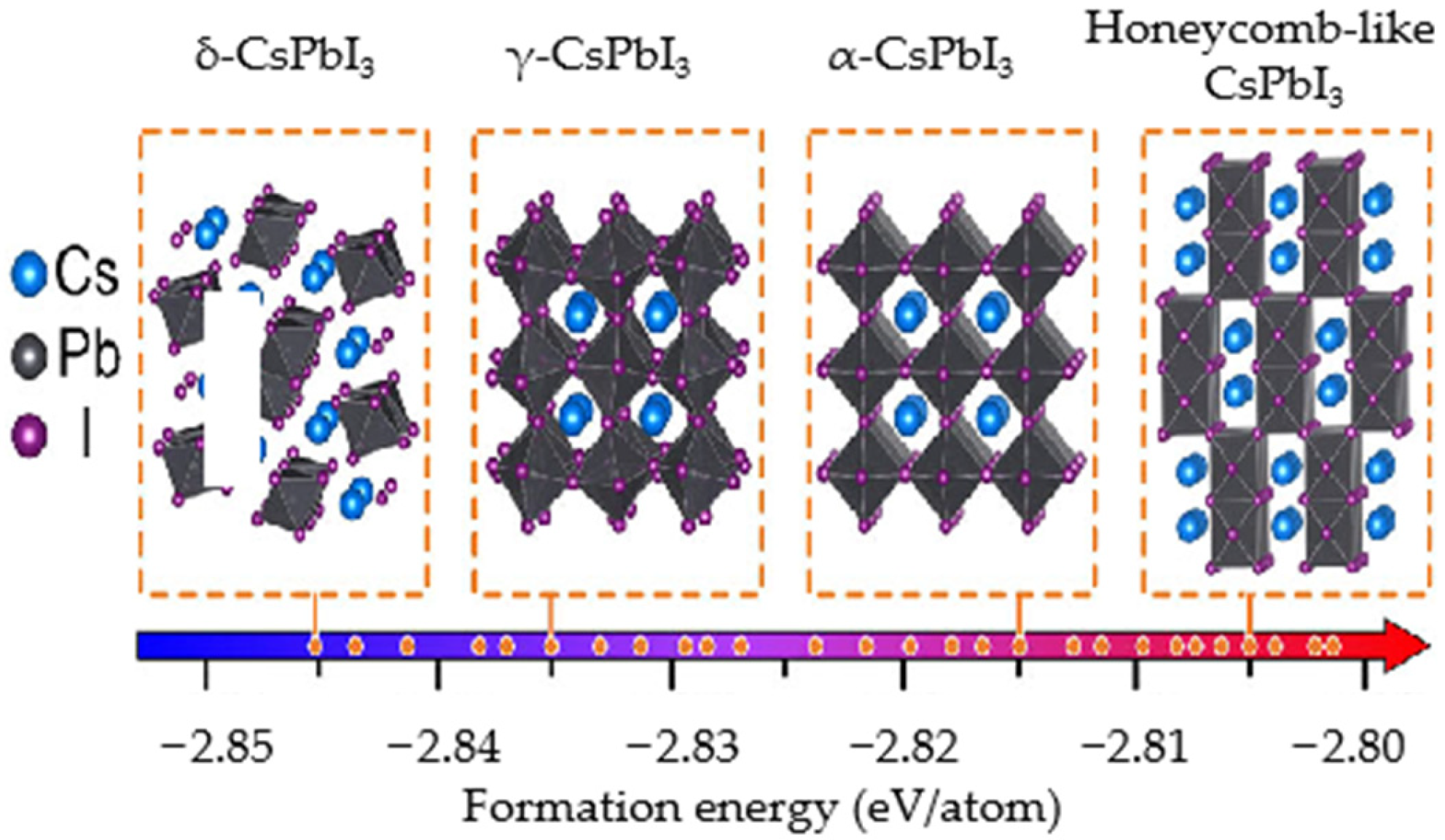
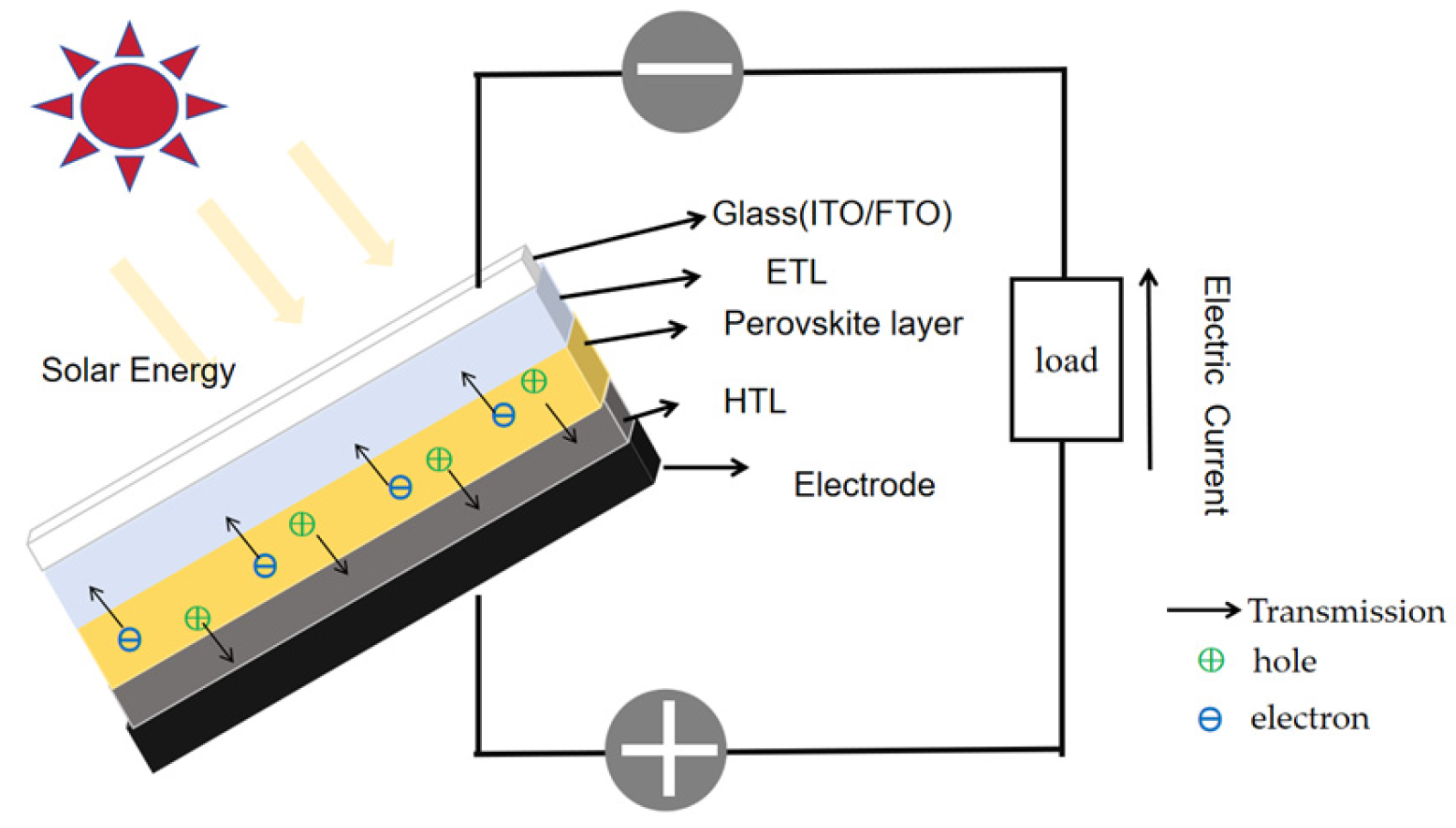
2. Structure and Working Principle of ISPCs

Structure of ISPCs

The CsPbX3 perovskite has four different polycrystalline configurations corresponding to different crystal phases. Taking CsPbI3 perovskite as an example, it has four crystal phases: cubic phase (α phase), tetragonal phase (β phase, space group), and two orthorhombic phases (γ phase and δ phase), as shown in Figure 2. Among them, the α, β, and γ phases have a perovskite structure and can exhibit excellent optoelectronic properties, generally referred to as the black phase, while the δ phase has a non-perovskite structure and does not possess optoelectronic properties, usually called the yellow phase. The bandgap width of the perovskite CsPbI3 thin film with the α, β, and γ phases structure is approximately 1.7 eV and appears black, showing good optoelectronic conversion efficiency; the bandgap width of the δ phase is about 2.75 eV, appearing yellow, and is not suitable as an absorber layer for solar cells. Perovskites typically exhibit octahedral distortion from the cubic phase to several symmetric reduced phases. The crystal structure of the α phase of CsPbI3 is only stable at high temperatures, and as the material cools, its chemical composition remains stable but the crystal structure collapses, transforming into the β phase; as the material temperature further decreases, the lower symmetry orthorhombic phase γ phase is also produced, still exhibiting the black phase and possessing optoelectronic properties; after the complete collapse of the crystal structure, it transforms into the non-optoelectronic δ phase, appearing yellow without optical activity [22,23]. This change in crystal structure caused by phase transition affects the separation and transportation of photo-generated charge carriers, which is the main reason for the decrease in battery performance and lifespan. However, the phase instability of CsPbX3 (such as CsPbI3 and CsPbI2Br) is a major obstacle to the development of IPSCs [24], mainly due to the non-ideal tolerance factor of the perovskite phase. The geometric stability of the CsPbX3 crystal structure can be evaluated by the Goldschmidt tolerance factor (t) and the octahedral factor (µ) [25], given by the following equation:
t = R A + R X 2 ( R B + R X ) ,
μ = R B R X ,
Among them, RA, RB, and RX represent the ionic radii of A, B, and X sites, respectively. The formation of perovskite structure requires keeping the values of t and μ within a reasonable range. When 0.9 < t < 1.107, an ideal α-phase perovskite structure can be formed. When 0.813 < t < 0.9, the tilting of the octahedra [PbX6]4− leads to distortion of the perovskite structure and the formation of asymmetric β or γ phases. Therefore, for different perovskite phases, optically active perovskite structures can be formed when 0.813 < t < 1.107 and 0.377 < μ < 0.895.
All-inorganic perovskite solar cells are mainly composed of a transparent conductive layer, an electron transport layer (ETL), a perovskite light-absorbing layer, a hole transport layer (HEL), and electrodes. The commonly used materials for the electron transport layer include tin dioxide (SnO2), titanium dioxide (TiO2), zinc oxide (ZnO), and fullerene derivatives (PCBM). TiO2 generally requires a higher annealing temperature, while SnO2 can be prepared at a lower temperature. Liu [26] used SnO2 as the electron transport layer to prepare CsPbI3-PSC, achieving a PCE of 15.5%. Due to the bipolar charge transport characteristics of perovskite materials, they can transfer electrons and holes while absorbing sunlight. Based on this characteristic, PSCs can be divided into two types: positive-type structure (n-i-p structure) and inverted-type structure (p-i-n structure), with the positive-type structure further divided into mesoporous and planar heterojunction structures. In the n-i-p mesoporous structure, there are many loose holes, which increase the effective contact area between TiO2 and perovskite, promoting the transfer and separation of charge carriers; at the same time, perovskite thin films prepared based on mesoporous structures have more uniform grain sizes, resulting in lower hysteresis effects in the solar cell devices. However, HTL materials may fill the pores, causing direct contact between ETL and HTL, leading to leakage current and a decrease in the open-circuit voltage of the solar cell devices. IPSCs with n-i-p planar structures have the advantages of a simple preparation process, low production cost, and high open-circuit voltage, but they suffer from severe hysteresis effects. The efficiency of IPSCs prepared with p-i-n planar structures is significantly lower than that of i-p-n planar structures, but it greatly reduces the hysteresis phenomenon of IPSCs. The J-V hysteresis in perovskite solar cells is mainly caused by the following reasons: (1) ion migration within the perovskite layer; (2) high trap density of electron carriers at the perovskite surface; and (3) an imbalance of carrier transport within the perovskite absorber. In the TiO2 electron transport layer commonly used in n-i-p structured perovskite solar cells, the significantly lower electron mobility compared to the commonly used hole transport materials leads to severe hysteresis effects in perovskite devices [27]. Yang et al. [28] optimized the surface of the TiO2 layer with 1-butyl-3-methylimidazolium tetrafluoroborate ionic liquid (IL) which has high optical transparency and superior electron mobility. This not only greatly improved the efficiency of the solar cell (certified PCE of 19.42%) but also eliminated the hysteresis effect. The reason may be that the anion groups of IL bind to TiO2, resulting in higher electron mobility and achieving a balance with hole mobility. At the same time, the cationic groups of IL provide an effective channel for electron transfer at the interface of adjacent perovskite particles, creating a suitable environment for growing perovskite with low trap density, thus improving device performance.
The principle of IPSCs (Figure 3): When sunlight shines on the IPSCs, the perovskite layer is excited by photons, generating electron–hole pairs. The asymmetric distribution of carrier concentration in the perovskite layer caused by the n-type and p-type transport layers drives the electrons and holes to dissociate at the interface between the perovskite layer and the transport layer, generating free electrons and free holes. The electrons enter the electron transport layer, the holes enter the hole transport layer, and then they reach the ITO and counter electrodes, respectively, along ETL and HTL, forming a potential difference. A current is generated through the external circuit to convert light energy into electrical energy.

3. Preparation Method of Perovskite Thin Films

For IPSCs, to effectively prevent the short-circuit phenomenon caused by defects, it is necessary to prepare CsPbX3 perovskite thin films that are continuous, uniform, with precise and controllable thickness, and without pinholes or cracks, so that the constructed IPSC has better optoelectronic performance [29]. The most commonly used method for preparing perovskite thin films is the solution method. The solution method is divided into the one-step method and two-step method. In addition, there is also the thermal evaporation method and vacuum evaporation method suitable for large-scale production.

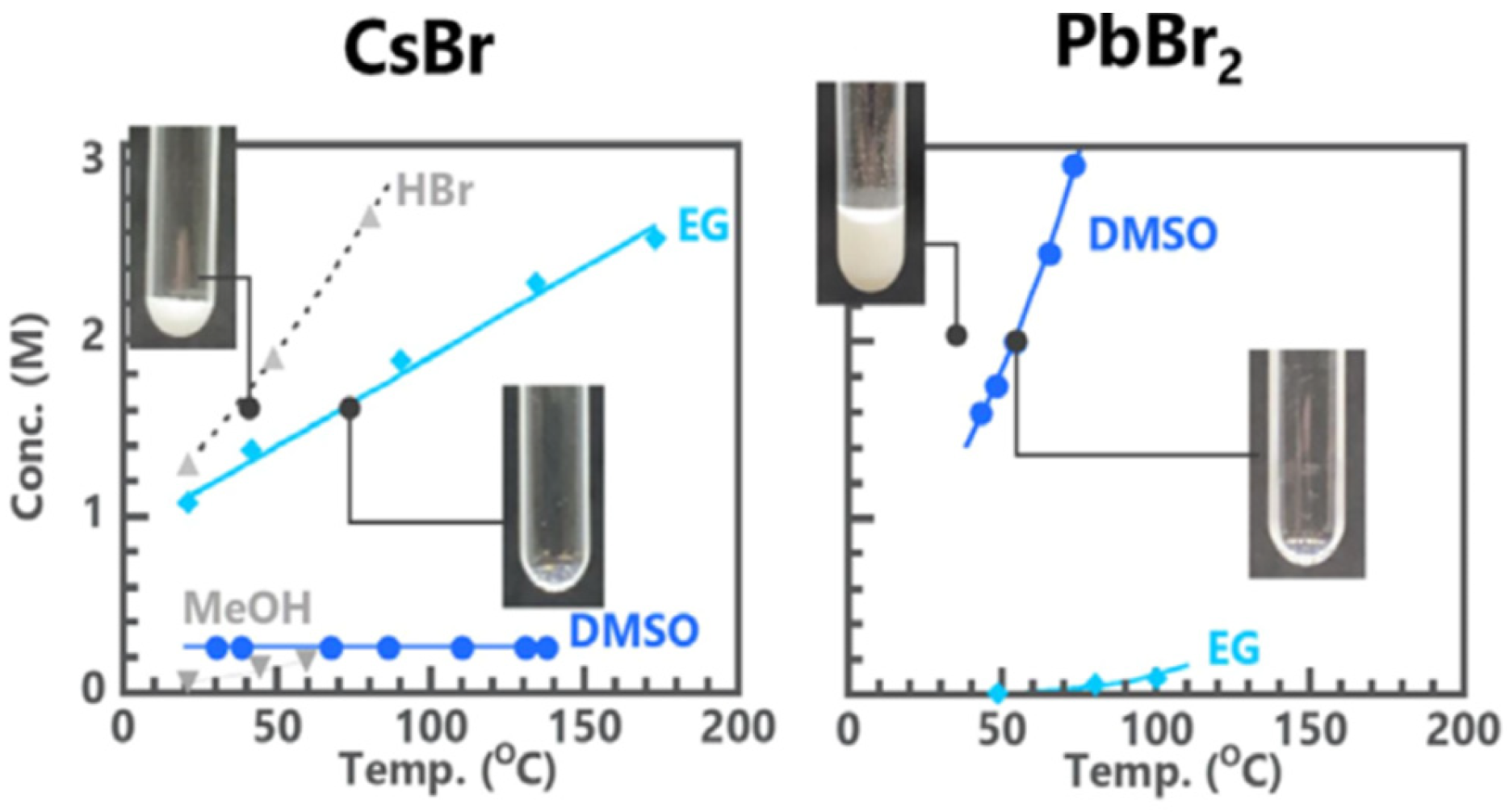
3.1. One-Step Method

The one-step method is one of the earliest methods used to prepare perovskite thin films, it usually refers to dissolving a fixed ratio of CsPbX3 perovskite precursor in a solvent, spin-coating or blade-coating on a substrate, and annealing to form a perovskite thin film. The most commonly used solvents for this method are dimethylformamide (DMF), dimethyl sulfoxide (DMSO), or a mixture of both [30]. The one-step method is the simplest operation, and large crystal phase grains of perovskite thin films can be prepared, but it has certain application defects. In the preparation of CsPbX3 perovskite thin films, CsX has low solubility and there is a large difference in solubility between CsX and PbX2 in DMSO (as shown in the Figure 4) [31]. Low-concentration CsX solution results in thin perovskite films that are too thin to absorb enough light for photovoltaic applications. And it is difficult to control the crystallization process of perovskite, often resulting in perovskite thin films with a large number of pinholes. The quality of the perovskite thin film is closely related to the crystal growth process [32]. Uneven nucleation and rapid crystal growth usually lead to small grain size, high grain boundary density, and poor surface morphology, so it is necessary to optimize crystal growth, suppress defects, and improve the photovoltaic parameters of the device. The film performance can be improved by adding anti-solvents during the spin-coating process to adjust the crystal growth rate, for example, adding ethyl acetate, chlorobenzene, benzene, toluene, isopropanol, etc. Zhang et al. [33] used ethyl acetate as an anti-solvent to induce the crystallization of CsPbBr3−XIX, and the efficiency of the IPSCs treated with anti-solvent increased from 4.51% to 8.60%. In addition to using a single anti-solvent, better effects can be achieved by using anti-solvents with synergistic effects. Yang et al. [34] used a mixed solution of chlorobenzene and isopropanol as an anti-solvent to prepare CsPbIBr2 thin films. The results show that the film modified with mixed anti-solvents has better morphology, crystallinity, sunlight absorption, lower trap density (N trap), and suppressed charge carrier recombination. The modified IPSCs without a hole transport layer achieved a champion efficiency of 7.05%, which is 28.18% higher than the original IPSCs without anti-solvents.

3.2. Two-Step Method

The two-step method first spin-coats the PbX2 precursor solution on the IFO/ITO conductive glass, and then immerses/spin-coats/drops the CsX solution to allow for a chemical reaction between the two, followed by annealing to produce all-inorganic perovskite materials. CsX is difficult to dissolve in common solvents, especially CsBr, but the problem of low solubility of CsBr can be solved by adjusting the immersion time and precursor concentration. Therefore, compared to the one-step method, this method usually produces better film morphology. The two-step method was first proposed by McMeekim et al. [35], who found that the repetition of CsBr droplets had an impact on the perovskite film and produced stable CsPbBr3 solar cells with a PCE of 9.72%. Wan et al. [36] used the two-step spin-coating method to spin-coat a CsBr methanol/H2O mixed solvent solution on the PbBr2 film, obtaining a dense and uniform CsPbBr3 film, and prepared an IPSC with good humidity and heat stability, with a maximum conversion efficiency of 8.11%. The two-step method can improve the crystallinity and interlayer surface coverage of thin films, with high repeatability and stability, and can produce high-efficiency, large-area perovskite solar cells. However, the obtained crystal phase particles are generally smaller, and the crystalline performance is not as good as the one-step method. At the same time, the two-step method requires a more complex preparation process and annealing environment, and precise control of the spin-coating process or immersion step in the second step is needed to obtain high-quality perovskite thin films.

3.3. Other Methods

Both thermal evaporation and vacuum deposition methods are suitable for producing large-area all-inorganic perovskite thin films. The thermal evaporation method is simple to operate, but it is difficult to precisely control the stoichiometry of halides, making it challenging to control the composition of the perovskite. It is mostly used for producing CsPbBr3 and CsPbI3 perovskite thin films. Mali et al. [37] used integrated hot air and triple-source thermal evaporation deposition technology to propose and develop β-CsPbI3 assisted by dimethylammonium iodide and γ-CsPbI3 assisted by guanidinium iodide all-inorganic phase heterojunction solar cells, achieving a PCE of 21.59%; meanwhile, when the effective area of the IPSC in the laboratory is 18.08 cm2, the PCE can reach 18.43%, with good stability, suitable for large-scale production. The vacuum deposition method requires relatively precise and complex instruments, making it easy to prepare large-area multilayer thin films with good uniformity and flatness, and can precisely control the thickness of the thin film. Liu et al. [38] prepared CsPbBr3 thin films using the vacuum deposition method by adding barium iodide additives, with the barium iodide diffusing into the lattice, reducing the defect density, adjusting the Fermi level, improving the band alignment, and obtaining high-performance IPSCs, with an efficiency of 10.09%. To ensure uniform film quality on a larger substrate, Zhang [33] investigated the effect of precursor solution concentration on the morphology of perovskite thin films. They found that a precursor solution concentration of 0.63M allowed for continuous coverage of the entire bottom substrate with inorganic perovskite thin films. Yang [34] studied the impact of a mixed anti-solvent of chlorobenzene (CB) and isopropanol (IPA) on perovskite thin films. By comparing the photovoltaic parameters of devices treated with anti-solvents at different volume ratios, they found that an IPA:CB ratio of 0.08:1 resulted in a continuous and uniform perovskite thin film, achieving a power conversion efficiency of 7.05%.

4. Hole Transport Layer and Electrode Material

4.1. Hole Transport Layer

The transport material of the hole is an important part of the PSC, which plays a key role in the extraction and transport of carriers, as well as in the suppression of carrier recombination. At the same time, in the n-i-p PSC, the hole transport layer can effectively block the electrode from direct contact with the perovskite layer, preventing moisture from the air from migrating to the perovskite layer, thus protecting the perovskite layer. It also helps to prevent ion migration in the perovskite material and improve the stability of the battery. The hole transport layer is divided into organic and inorganic hole transport layers. Organic hole transport layers generally refer to spiro-OMeTAD, PEDOT:PSS, P3HT, and polytriarylamine (PTAA). Inorganic hole transport layers include NiOX, CuI, CuSCN, NiO, graphene, PCBTDPP, carbon nanotubes, two-dimensional MXene materials, and so on. The initially used hole transport layer was spiro-OMeTAD [2], which significantly improved the optoelectronic performance of the PSCs, but its high cost and hygroscopic and deliquescent nature can lead to a decrease in the optoelectronic performance and instability of the PSC device. Therefore, research on inorganic hole transport layers or hole-free PSC devices with good prospects for development and commercial value has begun. Research on Cu-based and carbon-based hole transport layers is the most extensive. Noman et al. [39] conducted a study on three copper-based (SrCu2O2, CuSCN, and CuSbS2) and two carbon-based (C60 and PCBM) hole transport materials for perovskite using a solar cell capacitance simulator (SCAPS) one-dimensional simulation method. They found that the efficiency of SrCu2O2/perovskite layer/PCBM was the highest, with an efficiency of 26.48%. Liu et al. [40] synthesized CuS-MXene composites in situ using molecular self-assembly technology and used them as the hole transport layer for CsPbBr3-PSC, achieving an IPSC that can work in high-humidity conditions and has thermal stability with a PCE as high as 10.51%. After storage in high-humidity (85% RH) or high-temperature (85 °C) air for 30 days, the initial efficiency could still be maintained at over 90%. The experimental results show that the CuS-MXene composite optimizes the device interface energy levels of CsPbBr3-IPSC, constructs a CsPbBr3→CuS→MXene interface to passivate the surface defect states of the perovskite, promotes hole extraction, and effectively suppresses charge recombination.

4.2. Electrode Material

The electrode is an indispensable part of PSCs, which can effectively transmit and collect charge carriers to maintain the normal operation of photovoltaic devices. Traditional electrodes are mainly made of precious metals such as Au. However, the production cost of precious metals is high, which is not conducive to commercialization. The stability issues of metal electrodes (Al, Ag, Au, etc.) also need to be considered. For example, perovskite can chemically react with Ag and Au, leading to ion migration and reducing long-term stability. Since the work function of carbon (−5.0 eV) is close to that of gold (−5.1 eV), carbon deposited on CsPbBr3 perovskite film can effectively extract and collect holes. Now people are starting to use low-cost and stable carbon materials, such as carbon (graphene and graphite) [41], to replace expensive precious metal materials. Wei [42] introduced a flexible thermoplastic carbon film into PSCs, and due to its thermoplastic nature, the efficiency of the hole transport layer in PSCs reached 13.53%. This flexible carbon electrode has the advantages of low cost, simplicity, a low-temperature (<100 °C) preparation process, and high efficiency, and it has great potential for application in perovskite solar cells.

5. Optimization of the Photovoltaic Performance of IPSCs

CsPbX3 mainly includes four common types: CsPbI3, CsPbI2Br, CsPbIBr2, and CsPbBr3. Taking CsPbI3 as an example, the α phase generally needs to be obtained at a high temperature of 360 °C, while the tetragonal β phase and orthorhombic γ phase can be obtained at temperatures of 100~200 °C, and the δ phase can stably exist at room temperature. However, the α, β, and γ phases of CsPbI3 are unstable at room temperature, hindering their practical application. To improve the optoelectronic performance and long-term stability of photovoltaic devices, doping ions, interface modification, and other methods can be used for improvement.

5.1. Doping Ions

The doping of elements is an effective method to improve the quality, stability of the lattice, and charge transfer efficiency of all-inorganic perovskite thin films. Since CsPbI3 perovskite is prone to phase transition, the main purpose of doping CsPbI3 is to improve its phase stability, while doping CsPbBr3 is mainly to reduce its lattice defects or adjust its band gap width to increase light absorption, thereby optimizing device performance. For the all-inorganic CsPbX3 (X: Cl, Br, I) perovskite structure, larger A-site ions and smaller B-site doping ions can increase the Goldschmidt tolerance factor of perovskite, which is beneficial for forming more stable perovskite grains. Therefore, doping ions in the perovskite lattice to optimize the optoelectronic properties of all-inorganic perovskite materials and enhance the stability of the generated phases has a high feasibility.

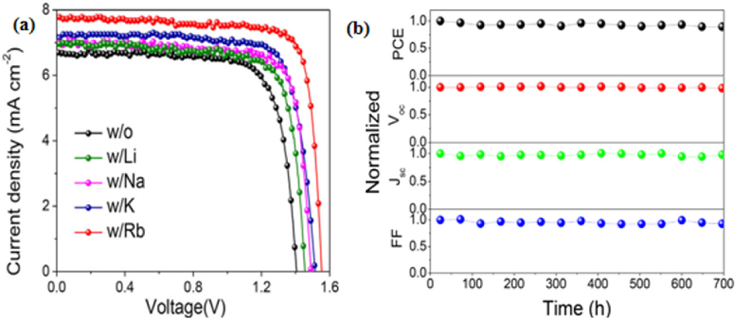
5.1.1. Doping of A-Site Ions

In the doping of A-site ions, researchers can choose various alkali metal cations (R = Li, Na, K, Rb) to optimize the lattice size and energy levels of halide Cs1−XRXPbX3 by adjusting the Cs/R ratio. Li et al. [43] doped alkali metal cations (Li, Na, K, and Rb) into the inorganic CsPbBr3 perovskite film at the A-site (Figure 5), where Rb+ doping formed a Cs0.91Rb0.09PbBr3 thin film. The no HTL IPSC with the best performance was prepared with the thin film containing Rb+ doping, which improved the stability of the perovskite film and optimized the optoelectronic properties. The PCE of the IPSCs increased from 7.28% to 9.86%, and even after 700 h at 80% humidity, it still maintained 97% of its initial efficiency. Moreover, A-site doping can also reduce the hysteresis effect of IPSCs. Hua [44] explored the influence of monovalent alkali metal (Li+, Na+, K+, Rb+) on the performance of CsPbBr3-PSCs and it is shown that doped Rb ions can significantly improve the crystallinity of perovskite, improve the device efficiency, and reduce the hysteresis. With the doping of smaller alkali metal cations, the effect of reducing the hysteresis effect is weaker. This phenomenon may be attributed to the ion-size effect. The larger Rb ions are not easily driven in the electric field compared to K, Na, and Li.

5.1.2. Doping of B-Site Ions

For B-site ion doping, according to the tolerance factor formula, it is necessary to use metal ions with ionic radii between 89 pm and 123 pm, such as the same-group elements Ge and Sn; group IIA elements Mg, Ca, Sr, and Ba; group VA elements Bi and Sb; group IIIA element In; and transition metal element Cu for doping [45]. B-site ion doping can optimize lattice defects, improve phase stability, and optimize optoelectronic properties. Ma et al. [46] used Zr4+ to replace B-site Pb2+ in CsPbI2Br to form CsPb1−XZrXI2Br IPSCs, which suppressed the transformation from the crystalline black α phase to the non-optically active δ phase and improved phase stability and thermal stability; at the same time, Zr4+ inhibited non-radiative recombination and optimized the matching energy levels with the hole transport layer, so that CsPbI2Br-IPSC doped with 4% ZrCl4 exhibited 16.60% efficiency at a high open-circuit voltage of 1.29 V (Figure 6). In addition, B-site ion doping can also reduce the toxicity of IPSCs and promote sustainable development [47]. Chen et al. [48] prepared a series of CsPb1−XSnXI2Br perovskites with tunable bandgaps from 1.92 eV to 1.38 eV. Extraordinarily, CsPb0.55Sn0.45I2Br showed the best thermal stability, and the all-inorganic Sn-Pb PSCs prepared exhibited a power conversion efficiency of 5.44%, as shown in Figure 7(Aa). However, Sn2+ is easily oxidized to Sn4+ by H2O and O2, leading to defects in the perovskite film, so further research is needed to prevent the oxidation of Sn2+ and to prevent water and oxygen. By reconstructing the grain boundaries with CsCl to reduce defect sites (I vacancies and Sn4+ cations), passivating Pb2+ with PbSO4, and producing hydrophobicity, a power conversion efficiency of 10.39% was achieved (Figure 7(Ab)). In the CsPbX3 perovskite layer doped with Sn2+, the oxidation of Sn2+ to Sn4+ introduces a large number of Sn vacancies, increases trap density, leads to p-type doping, and exacerbates non-radiative recombination losses. Therefore, it is necessary to take protective measures to prevent the oxidation of Sn2+ in tin-doped perovskite. In addition to the synergistic strategy of grain boundary reconstruction and surface coordination on the perovskite surface mentioned above, it has also been considered to add Sn2+ oxidation inhibitors to the precursor solution for perovskite preparation to prevent oxidation from the source. There are also others who have conducted research in this area. Liu et al. introduced 2-cyanoethylammonium iodide (CNI) into the halide tin-based perovskite film, using the strong coordination interaction between cyano (CeqN) and Sn2+ to inhibit the oxidation of Sn2+, resulting in reduced non-radiative recombination and lower trap density in the perovskite film [49] (Figure 7B). Wang and his colleagues [50] attempted to introduce a suitable amount of multifunctional tin oxalate (SnC2O4) to prepare efficient and stable Sn-Pb mixed IPSCs. SnC2O4 can compensate for Sn2+ and reducible oxalate ions C2O42−, effectively passivating both cationic and anionic defects, thus generating more n-type perovskite films. A relatively new continuous surface treatment method can also be considered—Surface Sn(IV) Hydrolysis (SSH)—to prevent tin oxidation. For example, Hu et al. [51] used Sn2+ halides treatment to replace buried Sn4+ ions beneath the film surface, followed by hydrolysis with H2O to replace the Sn4+ ions. In the SSH method, a relatively low concentration of SnX2 in isopropanol (IPA) solution is first prepared. The IPA solution of SnX2 is then spin-coated onto the surface of the CsPb0.6Sn0.4I3 thin film. The deposited SnX2 is expected to fill the tin vacancies (VSn) and iodine vacancies (VI) on the film surface. Additionally, due to the stronger chemical affinity of Sn(IV) for F, Cl, or Br compared to Sn(II), the Sn(IV) near the film surface region is reduced to Sn(II) through electron transfer. Subsequently, the IPA solution containing a small amount of water is spin-coated to hydrolyze and extract the Sn(IV), in situ forming an n-type electron-extracting SnOX layer. Some studies have also proposed doping with lanthanide ions. Duan et al. [52] recorded the time-resolved photoluminescence (TRPL) decay curves of various Ln3+ ion (Ln3+ = Sm3+, Tb3+, Ho3+, Er3+, and Yb3+)-doped perovskite thin films, as shown in Figure 7C. After doping with Ln3+ ions, the average lifetime of the PCE increased by nearly 1.5 times, indicating that non-radiative pathways were partially eliminated, which is beneficial for improving the output of IPCE.

5.2. Interface Modification

Interface modification is a common method to optimize the photovoltaic performance of IPSCs. It can effectively optimize the charge input pathway and reduce charge recombination, thereby improving the photovoltaic performance of the device. The interface modification of IPSCs can be roughly divided into two categories: one is to weaken charge recombination, and the other is to improve the light absorption capacity of the battery. There are mainly two types of interfaces in IPSCs: one is the buried interface (BIF), which refers to the interface modification between the perovskite layer and the ETL in the n-i-p type structure of IPSCs, and the other is the surface of the perovskite. Research has shown that the perovskite BIF is key to limiting the quality of perovskite thin films and the efficiency of devices [53]. Due to continuous solution and temperature erosion, the bottom surface of the perovskite is more prone to interface defects than the body surface and upper surface of the perovskite [54]. Therefore, by modifying the BIF, the crystalline growth of the perovskite can be controlled, light-generated carriers can be extracted, and band energy can be adjusted for energy matching. There are several characterization techniques for obtaining interface information between the transport layer and perovskite materials: atomic force microscopy imaging technology to analyze the surface roughness of the interface, cold field emission scanning electron microscopy technology to analyze the surface and cross-sectional morphology of the perovskite layer; X-ray powder diffraction method to determine the crystal structure and crystalline properties of the perovskite; using the Kyowa DropMaster optical contact angle measuring instrument to measure the contact angles (CAs) of water droplets on the modified film; analyzing the water resistance performance of the film; etc. For example, Yu [55] used a urea ammonium thiocyanate (UAT) molten salt modification strategy, fully utilizing the synergistic activity of thiocyanate salts, to prepare high-quality CsPbI3 films. Characterization techniques using XRD, SEM, and atomic force microscopy revealed that UAT enhanced the XRD diffraction peak intensity of CsPbI3 film, significantly improved the morphology of the film, making it more uniform, and it had a smaller surface roughness (Ra = 18.7 nm) compared to the unmodified film (Ra = 22.3 nm).

5.2.1. Weakening Charge Recombination

Due to the characteristic of halides and their derivatives to react with Pb2+ and achieve passivation of the crystal interface, weakening the effect of charge recombination, they are promising interface modification materials. Ho et al. [56] inserted quaternary ammonium halide derivatives (PQCl) into the oxygenated nickel (NiOX) layer and perovskite layer in the inverted structure PSCs, also with BIF modification. The stratification of PQCl between NiOX and perovskite layers improved the interface contact, promoted crystal growth, and passivated the interface and crystal defects, thereby weakening the interface recombination. The PQCl-modified inverted PSC showed excellent photovoltaic performance, with a PCE of 14.40%, an open-circuit voltage of 1.06 V, a short-circuit current density of 18.35 mA/cm3, and a fill factor of 74.0% (Figure 8A). Chu et al. [57] used cesium fluoride (CsF) to in situ reconstruct the surface of inorganic perovskite, obtaining an IPSC efficiency of 21.02%, an open-circuit voltage as high as 1.27 V, and a fill factor of 85.3%. The research results indicate that this strategy suppresses non-radiative recombination while promoting hole extraction; the introduced fluorine can effectively passivate surface defects, extending the carrier lifetime from 11.5 ns to 737.2 ns (Figure 8B).
In addition, highly coordinated thiocyanate salts have also been found to have a very positive regulatory effect on perovskite thin films. Yu et al. [55] used the synergistic activity of urea thiocyanate ammonium (UAT) molten salt to modify CsPbI3 thin films, significantly improving the crystal quality of CsPbI3 thin films and achieving a long single exponential charge recombination lifetime of over 30 ns. The efficiency of the modified PSC has been increased to over 20% (steady-state efficiency is 19.2%), with good operational stability for over 1000 h, as shown in Figure 8C. Zhang [58] prepared high-quality γ-CsPbI3 perovskite thin films through co-evaporation of PbI2 and CsI with a small amount of phenylethylammonium iodide (PEAI). The incorporation of PEAI resulted in the formation of some columnar grains on the surface of the perovskite thin film, which can fill the defect sites of the film, significantly improving γ-CsPbI3, reducing trap density, and suppressing non-radiative recombination losses. The PEAI-γ-CsPbI3 PSCs achieved a PCE of 15% and exhibited superior stability, maintaining 80% of their initial performance after 165 h of continuous light illumination, while the γ-CsPbI3 without PEAI rapidly degraded after 30 h and transformed into the δ phase, losing its photovoltaic performance.

5.2.2. Optimize the Light Absorption Capacity and Charge Transfer Capability of Cells

In addition, using compounds with excellent light absorption properties can optimize the light absorption capacity of batteries, while polar molecule materials can enhance charge transfer capability through interface modification. Wu [59] utilized the BIF modification of 4,4-difluoro cyclohexylamine hydrochloride (abbreviated as DFCHY). Theoretical analysis and experimental results show that DFCHY plays an important role in bridging the NiOX/perovskite interface, not only suppressing the high oxidation state of Ni3+ and improving the conductivity of NiOX film but also passivating the perovskite film’s BIF, enhancing its crystallinity, further effectively reducing the trap density at the NiOX/perovskite layer interface, decreasing non-radiative recombination, and enhancing charge transfer (Figure 9A). The PCE of the inverted PSC after passivation is 17.08%. Furthermore, the unencapsulated PSC after passivation exhibits excellent long-term stability, maintaining over 90% of its initial efficiency after 1000 h of storage in a nitrogen-filled glovebox. Liu [60] used natural dyes curcumin and beta-carotene as additives in a CsPbBr3 perovskite precursor solution for film optimization, increasing the absorption intensity of the film, adjusting the energy levels of the perovskite layer, optimizing the energy level matching of the device layers, and enhancing charge carrier transport. Morphological characterization of the film surface and cross-section revealed that the introduction of dyes increased the size of perovskite grains and significantly improved the film porosity. The PCE values of devices with added curcumin and beta-carotene were 9.78% and 7.81%, respectively, showing an improvement compared to the pure CsPbBr3 PCE of 5.35% (Figure 9B).
Wang [61] used phenethylamine cations (PEA+) as organic cations, and then conducted a typical cation exchange reaction on CsPbI3 using phenethylammonium iodide (PEAI) solution. PEA+ forms a surface cation termination at the top of α-CsPbI3, which can stabilize the phase transition of α-CsPbI3, enhance the stability of α-CsPbI3, and prevent the generation of 2D perovskite layers that hinder electron transfer. Even after annealing at 80 °C for 150 h, a-CsPbI3 exhibits enhanced phase stability, higher moisture resistance, and excellent electron transfer properties. Based on PEA+ terminated α-CsPbI3, PSCs achieved a champion stability efficiency of 13.5%, and after storage for one month without encapsulation, they still maintained a PCE of 13%. The more I in CsPbI3 is replaced by Br, the stronger the stability, but the stability of CsPbIBr2 at room temperature is still poor, which can be enhanced by additive engineering. Wu et. al. [62] used 1-butyl-3-methylimidazolium acetate (BMIMAc) ionic liquid to treat Tio2/CsPbIBr2 perovskite BIF, which improved the crystallinity of the perovskite film, adjusted the energy level alignment, and promoted electron extraction and transport, thereby increasing Voc. At the same time, BMIMAc can passivate defects related to Cs+/Pb2+ in the perovskite film, thus suppressing non-radiative recombination. The optimized CsPbIBr2 PSC has an efficiency of 10.30% and a Voc of 1.361 V, much higher than the control group perovskite solar cells (7.87% and 1.213 V). After accelerated degradation in air at 85 °C (RH: 50~60%) for 420 min, the optimized CsPbIBr2 PSCs can retain 92.7% of the original PCE.

6. Summary and Prospect

Inorganic CsPbX3-PSC has good optical and thermal stability, and its PCE has developed rapidly, reaching over 20%, with great potential for development [63]. However, it still faces problems such as poor phase stability of the perovskite crystal structure, high bandgap width (for example, the bandgap width of inorganic CsPbBr3 perovskite is 2.3 eV), the absorption intensity is not enough, and the energy levels do not match. In future research, the focus can be placed on the following aspects:
(1)
To address the issues of the organic hole transport layer being prone to moisture and the expensive and ion migration-prone nature of metal electrode materials, it can be resolved by using inorganic hole transport layers such as two-dimensional MeXene materials, PCBM, or researching carbon-based IPSCs without hole transport layers. This optimizes the energy level matching arrangement to enhance the charge transfer capability between the perovskite layer and the inorganic hole transport layer/carbon electrode, thereby improving the stability and optoelectronic performance of the device.
(2)
In response to the problem of CsPbI3 easily transforming from the α phase to the δ phase, by doping with small-radius elements and reducing the defect state density by passivating interface defects, the phase stability of CsPbI3 can be improved. In addition, increasing research on lead-free IPSCs is of great significance for environmental sustainability, and researching new lead-free perovskite solar cells is a necessary trend for future development.

Supplementary Materials

The following supporting information can be downloaded at https://www.mdpi.com/article/10.3390/en17112671/s1, Table S1: summarizing recently reported CsPbX3 IPSC information.

Author Contributions

Conceptualization, S.X. and L.Y.; methodology, X.Z.; software, S.X.; validation, S.X. and L.Y.; formal analysis, L.W.; investigation, S.X. and L.Y.; resources, L.Y.; data curation, L.W.; writing—original draft preparation, S.X.; writing—review and editing, X.Z. and W.S.; visualization, W.S.; supervision, X.Z.; project administration, X.Z.; funding acquisition, X.Z. All authors have read and agreed to the published version of the manuscript.

Funding

This research was funded by Hainan Provincial Natural Science Foundation of High Level-talent Project (220RC594) and the National Natural Science Foundation of China (22102043).

Conflicts of Interest

The authors declare no conflict of interest.

References

  1. Kojima, A.; Teshima, K.; Shirai, Y.; Miyasaka, T. Organometal Halide Perovskites as Visible-Light Sensitizers for Photovoltaic Cells. J. Am. Chem. Soc. 2009, 131, 6050–6051. [Google Scholar] [CrossRef]
  2. Kim, H.-S.; Lee, C.-R.; Im, J.-H.; Lee, K.-B.; Moehl, T.; Marchioro, A.; Moon, S.-J.; Humphry-Baker, R.; Yum, J.-H.; Moser, J.E.; et al. Lead Iodide Perovskite Sensitized All-Solid-State Submicron Thin Film Mesoscopic Solar Cell with Efficiency Exceeding 9%. Sci. Rep. 2012, 2, 591. [Google Scholar] [CrossRef]
  3. Han, Q.; Bae, S.H.; Sun, P.; Hsieh, Y.T.; Yang, Y.M.; Rim, Y.S.; Zhao, H.; Chen, Q.; Shi, W.; Li, G.; et al. Single Crystal Formamidinium Lead Iodide (FAPbI3): Insight into the Structural, Optical, and Electrical Properties. Adv. Mater 2016, 28, 2253–2258. [Google Scholar] [CrossRef] [PubMed]
  4. Zhang, P. All Inorganic Perovskite Solar Cells and Absorption Layer Band Gap Regulation. Master’s Thesis, Henan University, Zhengzhou, China, 2019. [Google Scholar]
  5. National Renewable Energy Laboratory. Best Research-Cell Efficiency Chart; National Renewable Energy Laboratory: Golden, CO, USA, 2024. Available online: https://www.nrel.gov/pv/cell-efficiency.html (accessed on 23 May 2024).
  6. Liang, Z.; Zhang, Y.; Xu, H.; Chen, W.; Liu, B.; Zhang, J.; Zhang, H.; Wang, Z.; Kang, D.-H.; Zeng, J.; et al. Homogenizing out-of-plane cation composition in perovskite solar cells. Nature 2023, 624, 557–563. [Google Scholar] [CrossRef] [PubMed]
  7. Bryant, D.; Aristidou, N.; Pont, S.; Sanchez-Molina, I.; Chotchunangatchaval, T.; Wheeler, S.; Durrant, J.R.; Haque, S.A. Light and oxygen induced degradation limits the operational stability of methylammonium lead triiodide perovskite solar cells. Energy Environ. Sci. 2016, 9, 1655–1660. [Google Scholar] [CrossRef]
  8. Chen, Y.-C.; Lin, W.-J.; Chiu, C.-C.; Juwita, R.; Tsai, H.-H.G. First-Principles Investigation of the Thermal Degradation Mechanisms of Methylammonium Lead Triiodide Perovskite. J. Phys. Chem. C 2020, 124, 14521–14530. [Google Scholar] [CrossRef]
  9. Juarez-Perez, E.J.; Ono, L.K.; Maeda, M.; Jiang, Y.; Hawash, Z.; Qi, Y. Photodecomposition and thermal decomposition in methylammonium halide lead perovskites and inferred design principles to increase photovoltaic device stability. J. Mater. Chem. A 2018, 6, 9604–9612. [Google Scholar] [CrossRef]
  10. Akbulatov, A.F.; Luchkin, S.Y.; Frolova, L.A.; Dremova, N.N.; Gerasimov, K.L.; Zhidkov, I.S.; Anokhin, D.V.; Kurmaev, E.Z.; Stevenson, K.J.; Troshin, P.A. Probing the Intrinsic Thermal and Photochemical Stability of Hybrid and Inorganic Lead Halide Perovskites. J. Phys. Chem. Lett. 2017, 8, 1211–1218. [Google Scholar] [CrossRef]
  11. Imran, M.; Saleem, A.; Khan, N.A.; Kamboh, A.H. Enhanced efficiency and stability of perovskite solar cells by partial replacement of CH3NH3+ with inorganic Cs+ in CH3NH3PbI3 perovskite absorber layer. Phys. B Condens. Matter 2019, 572, 1–11. [Google Scholar] [CrossRef]
  12. Hsiao, Y.-W.; Wang, S.-Y.; Huang, C.-L.; Leu, C.-C.; Shih, C.-F. Resistive Switching Property of Organic–Inorganic Tri-Cation Lead Iodide Perovskite Memory Device. Nanomaterials 2020, 10, 1155. [Google Scholar] [CrossRef]
  13. Kulbak, M.; Cahen, D.; Hodes, G. How Important Is the Organic Part of Lead Halide Perovskite Photovoltaic Cells? Efficient CsPbBr3 Cells. J. Phys. Chem. Lett. 2015, 6, 2452–2456. [Google Scholar] [CrossRef] [PubMed]
  14. Kulbak, M.; Gupta, S.; Kedem, N.; Levine, I.; Bendikov, T.; Hodes, G.; Cahen, D. Cesium Enhances Long-Term Stability of Lead Bromide Perovskite-Based Solar Cells. J. Phys. Chem. Lett. 2015, 7, 167–172. [Google Scholar] [CrossRef]
  15. Swarnkar, A.; Marshall, A.R.; Sanehira, E.M.; Chernomordik, B.D.; Moore, D.T.; Christians, J.A.; Chakrabarti, T.; Luther, J.M. Quantum dot-induced phase stabilization of α-CsPbI3 perovskite for high-efficiency photovoltaics. Science 2016, 354, 92–95. [Google Scholar] [CrossRef] [PubMed]
  16. Xu, Y.; Li, G.; Jing, Y.; Zhang, H.; Wang, X.; Lu, Y.; Wu, J.; Lan, Z. n-type absorber by Cd2+ doping achieves high-performance carbon-based CsPbIBr2 perovskite solar cells. J. Colloid Interface Sci. 2022, 608, 40–47. [Google Scholar] [CrossRef] [PubMed]
  17. Xu, Y.; Li, G.; Li, R.; Jing, Y.; Zhang, H.; Wang, X.; Du, Z.; Wu, J.; Lan, Z. PbS/CdS heterojunction thin layer affords high-performance carbon-based all-inorganic solar cells. Nano Energy 2022, 95, 106973. [Google Scholar] [CrossRef]
  18. Xu, Y.; Liu, F.; Li, R.; Jing, Y.; Chen, Q.; Chen, X.; Deng, C.; Du, Z.; Sun, W.; Wu, J.; et al. Mxene regulates the stress of perovskite and improves interface contact for high-efficiency carbon-based all-inorganic solar cells. Chem. Eng. J. 2023, 461, 141895. [Google Scholar] [CrossRef]
  19. Gao, L.; Liu, F.; Li, R.; Yao, Q.; Jiang, D.; Zhong, C.; Lin, W.; Huang, M.; Wu, J.; Lan, Z. Multifunctional surface modification of carbon-based all-inorganic CsPbI2Br solar cells by 3-(trifluoromethyl) phenyltrimethyl ammonium iodide. J. Alloy. Compd. 2024, 989, 174374. [Google Scholar] [CrossRef]
  20. Chen, B.; Wang, P.; Ren, N.; Li, R.; Zhao, Y.; Zhang, X. Tin dioxide buffer layer-assisted efficiency and stability of wide-bandgap inverted perovskite solar cells. J. Semicond. 2022, 43, 052201. [Google Scholar] [CrossRef]
  21. Yue, M. Investigation on Light Management In Perovskite Solar Cells and Process Conditions of Inverted Cspbi3 Solar Cells. Master’s Thesis, University of Chinese Academy of Sciences, Beijing, China, 2022. [Google Scholar]
  22. Doherty, T.; Winchester, A.J.; Macpherson, S.; Johnstone, D.; Pareek, V.; Tennyson, B.; Kosar, S.; Kosasih, F.; Anaya, M.; Abdi-Jalebi, M.; et al. Performance-limiting nanoscale trap clusters at grain junctions in halide perovskites. Nature 2020, 580, 360–366. [Google Scholar] [CrossRef] [PubMed]
  23. Fu, P.; Hu, S.; Tang, J.; Xiao, Z. Material exploration via designing spatial arrangement of octahedral units: A case study of lead halide perovskites. Front. Optoelectron. 2021, 14, 252–259. [Google Scholar] [CrossRef]
  24. Steele, J.A.; Jin, H.; Dovgaliuk, I.; Berger, R.F.; Braeckevelt, T.; Yuan, H.; Martin, C.; Solano, E.; Lejaeghere, K.; Rogge, S.M.J.; et al. Thermal unequilibrium of strained black CsPbI 3 thin films. Science 2019, 365, 679–684. [Google Scholar] [CrossRef] [PubMed]
  25. Sun, Q.; Yin, W.-J. Thermodynamic Stability Trend of Cubic Perovskites. J. Am. Chem. Soc. 2017, 139, 14905–14908. [Google Scholar] [CrossRef] [PubMed]
  26. Liu, Y. Optimization of Light Absorption Layer for CsPbI3 All-Inorganic Perovskite Solar Cells Prepared by Low Temperature Solution Method. Master’s Thesis, Zhejiang Sci-Tech University, Hangzhou, China, 2023. [Google Scholar]
  27. Wali, Q.; Aamir, M.; Ullah, A.; Iftikhar, F.J.; Khan, M.E.; Akhtar, J.; Yang, S. Fundamentals of Hysteresis in Perovskite Solar Cells: From Structure-Property Relationship to Neoteric Breakthroughs. Chem. Rec. 2022, 22, e202100150. [Google Scholar] [CrossRef] [PubMed]
  28. Yang, D.; Zhou, X.; Yang, R.; Yang, Z.; Yu, W.; Wang, X.; Li, C.; Liu, S.; Chang, R.P.H. Surface optimization to eliminate hysteresis for record efficiency planar perovskite solar cells. Energy Environ. Sci. 2016, 9, 3071–3078. [Google Scholar] [CrossRef]
  29. Mao, P.; Zhou, Q.; Jin, Z.; Li, H.; Wang, J. Efficiency-Enhanced Planar Perovskite Solar Cells via an Isopropanol/Ethanol Mixed Solvent Process. ACS Appl. Mater. Interfaces 2016, 8, 23837–23843. [Google Scholar] [CrossRef] [PubMed]
  30. Kang, T.; Tsai, C.-M.; Jiang, Y.-H.; Gollavelli, G.; Mohanta, N.; Diau, E.W.-G.; Hsu, C.-S. Interfacial Engineering with Cross-Linkable Fullerene Derivatives for High-Performance Perovskite Solar Cells. ACS Appl. Mater. Interfaces 2017, 9, 38530–38536. [Google Scholar] [CrossRef] [PubMed]
  31. Satoshi, W.; Taiki, H.; Masaru, I.; Yusuke, I.; Masashi, K.; Tetsuya, K. Single Crystallization of Cs4PbBr6 Perovskite from Su-persaturated Organic Solutions Optimized Through Solubility Studies. ACS Omega 2023, 8, 2455–2461. [Google Scholar]
  32. Zhang, X.; Fei, C.; Shen, L.; Baral, P.; Vijayaraghavan, S.N.; Yan, F.; Gong, X.; Wang, H. Manipulating Nucleation and Crystal Growth of Inorganic Perovskite Solar Cells Manipulating Nucleation and Crystal Growth of Inorganic Perovskite Solar Cells. ACS Appl. Mater. Interfaces 2023, 15, 38522–38529. [Google Scholar] [CrossRef] [PubMed]
  33. Zhang, H. Study on the Preparation and Photoelectric Performance of High-Efficiency Inorganic Perovskite Solar Cells. Master’s Thesis, Hubei University, Wuhan, China, 2018. [Google Scholar]
  34. Yang, J.; Yu, H.; Wu, S.; Cai, C.; Gao, J.; Lu, X.; Gao, X.; Shui, L.; Wu, S.; Liu, J.-M. A Mixed Antisolvent-Assisted Crystallization Strategy for Efficient All-Inorganic CsPbIBr2 Perovskite Solar Cells by a Low-Temperature Process. ACS Appl. Energy Mater. 2022, 5, 2881–2889. [Google Scholar] [CrossRef]
  35. McMeekin, D.P.; Mahesh, S.; Noel, N.K.; Klug, M.T.; Lim, J.; Warby, J.H.; Ball, J.M.; Herz, L.M.; Johnston, M.B.; Snaith, H.J. Solution-Processed All-Perovskite Multi-junction Solar Cells. Joule 2019, 3, 387–401. [Google Scholar] [CrossRef]
  36. Wan, X.; Yu, Z.; Tian, W.; Huang, F.; Jin, S.; Yang, X.; Cheng, Y.-B.; Hagfeldt, A.; Sun, L. Efficient and stable planar all-inorganic perovskite solar cells based on high-quality CsPbBr3 films with controllable morphology. J. Energy Chem. 2020, 46, 8–15. [Google Scholar] [CrossRef]
  37. Mali, S.S.; Patil, J.V.; Shao, J.-Y.; Zhong, Y.-W.; Rondiya, S.R.; Dzade, N.Y.; Hong, C.K. Phase-heterojunction all-inorganic perovskite solar cells surpassing 21.5% efficiency. Nat. Energy 2023, 8, 989–1001. [Google Scholar] [CrossRef]
  38. Liu, Y.; Xiang, T.; Zhang, B.; Wang, J.; Yu, X.; Xiao, Y.; Xiao, J.; Ku, Z.; Peng, Y. Defect Passivation and Fermi Level Modification for >10% Evaporated All-Inorganic CsPbBr3 Perovskite Solar Cells. ACS Appl. Energy Mater. 2022, 5, 8049–8056. [Google Scholar] [CrossRef]
  39. Noman, M.; Shahzaib, M.; Jan, S.T.; Shah, S.N.; Khan, A.D. 26.48% efficient and stable FAPbI3 perovskite solar cells employing SrCu2O2 as hole transport layer. RSC Adv. 2023, 13, 1892–1905. [Google Scholar] [CrossRef]
  40. Liu, W.; Yao, X.; He, B.; Sui, H.; Wei, M.; Chen, H.; Duan, J.; Tang, Q. A self-assembled CuS-MXene bridge for hole-boosting 10.51% efficiency all-inorganic tri-brominated perovskite solar cell. J. Mater. Chem. A 2023, 11, 20206–20214. [Google Scholar] [CrossRef]
  41. Tan, J.; Dou, J.; Tang, Q. A photovoltaic hydrovoltaic coupled carbon-based, all-inorganic CsPbBr3 perovskite solar cell. Chem. Commun. 2023, 59, 4608–4611. [Google Scholar] [CrossRef]
  42. Wei, H.; Xiao, J.; Yang, Y.; Lv, S.; Shi, J.; Xu, X.; Dong, J.; Luo, Y.; Li, D.; Meng, Q. Free-standing flexible carbon electrode for highly efficient hole-conductor-free perovskite solar cells. Carbon 2015, 93, 861–868. [Google Scholar] [CrossRef]
  43. Li, Y.; Duan, J.; Yuan, H.; Zhao, Y.; He, B.; Tang, Q. Lattice Modulation of Alkali Metal Cations Doped Cs1−xRxPbBr3 Halides for Inorganic Perovskite Solar Cells. Sol. RRL 2018, 2, 1800164. [Google Scholar] [CrossRef]
  44. Hua, J. Preparation of CsPbBr3 Perovskite Solar Cells Based on Vacuum Evaporation Method. Master’s Thesis, Wuhan University of Technology, Wuhan, China, 2020. [Google Scholar]
  45. Li, Q.; Zhang, P.; Yao, L.; Deng, L.; Ren, X.; Li, Y. Research progress of less-lead/lead-free perovskite solar cells. J. Synth. Cryst. 2022, 51, 551–558. [Google Scholar] [CrossRef]
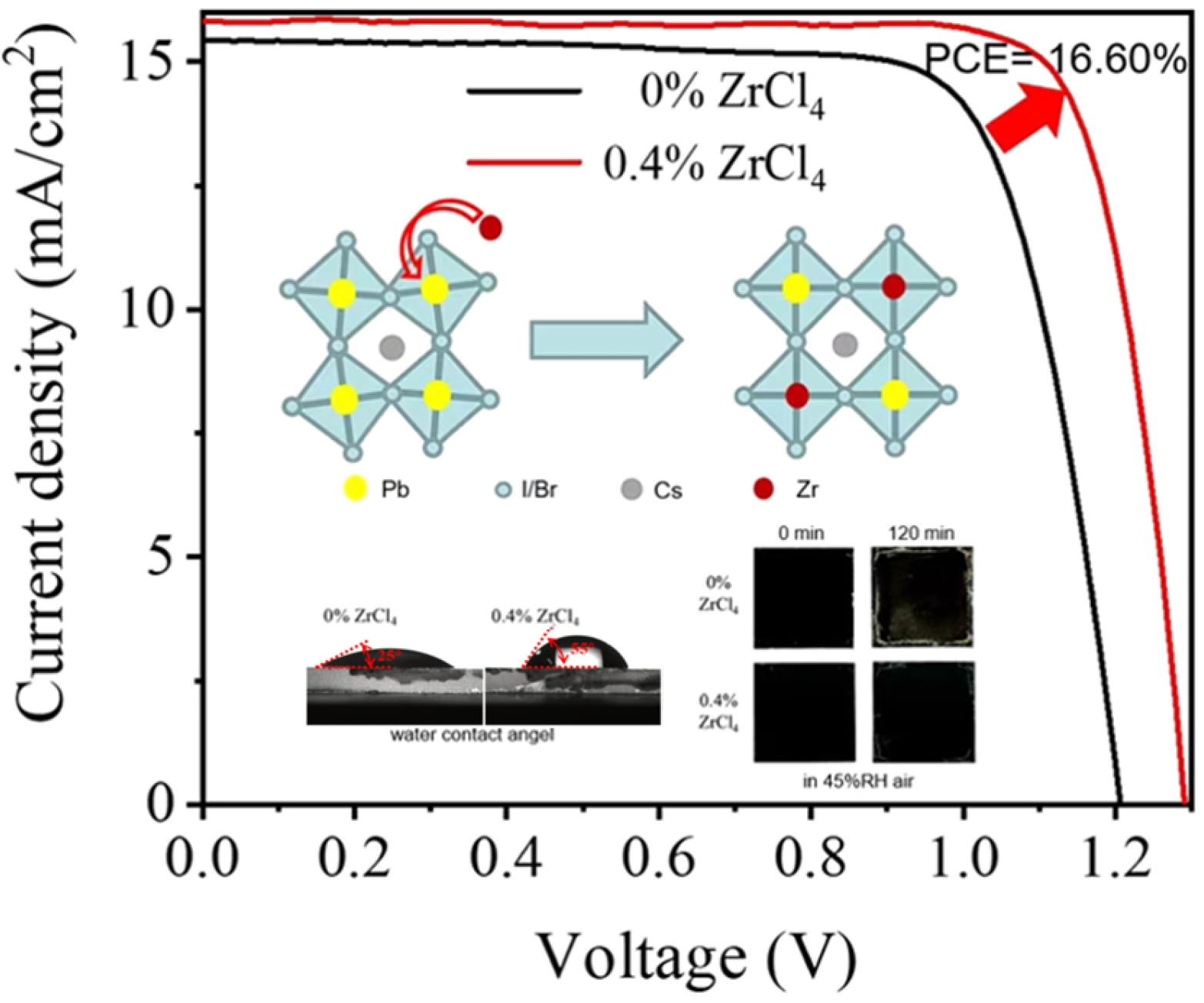
  46. Ma, P.; Bie, T.; Liu, Y.; Yang, L.; Bi, S.; Wang, Z.; Shao, M. Zirconium Doping to Enable High-Efficiency and Stable CsPbI2Br All-Inorganic Perovskite Solar Cells. ACS Appl. Mater. Interfaces 2024, 16, 1217–1224. [Google Scholar] [CrossRef]
  47. Abate, A. Perovskite Solar Cells Go Lead Free. Joule 2017, 1, 659–664. [Google Scholar] [CrossRef]
  48. Chen, G.; Li, P.; Xue, T.; Su, M.; Ma, J.; Zhang, Y.; Wu, T.; Han, L.; Aldamasy, M.; Li, M.; et al. Design of Low Bandgap CsPb1−XSnXI2Br Perovskite Solar Cells with Excellent Phase Stability. Small 2021, 17, 2101380. [Google Scholar] [CrossRef]
  49. Liu, T.; Wang, J.; Liu, Y.; Min, L.; Wang, L.; Yuan, Z.; Sun, H.; Huang, L.; Li, L.; Meng, X. Cyano-Coordinated Tin Halide Perovskites for Wearable Health Monitoring and Weak Light Imaging. Adv. Mater. 2024, e2400090. [Google Scholar] [CrossRef] [PubMed]
  50. Wang, Q.; Xiong, J.; Xing, Y.; Gan, X.; Zhu, W.; Xuan, R.; Liu, X.; Huang, L.; Zhu, Y.; Zhang, J. Reductive Sn2+ Compensator for Efficient and Stable Sn-Pb Mixed Perovskite Solar Cells. Adv. Sci. 2024, 2400962. [Google Scholar] [CrossRef]
  51. Hu, M.; Zhang, Y.; Gong, J.; Zhou, H.; Huang, X.; Liu, M.; Zhou, Y.; Yang, S. Surface Sn(IV) Hydrolysis Improves Inorganic Sn–Pb Perovskite Solar Cells. ACS Energy Lett. 2023, 8, 1035–1041. [Google Scholar] [CrossRef]
  52. Duan, J.; Zhao, Y.; Yang, X.; Wang, Y.; He, B.; Tang, Q. Lanthanide Ions Doped CsPbBr3 Halides for Htm-Free 10.14% Efficiency Inorganic Perovskite Solar Cell with an Ultrahigh Open-Circuit Voltage of 1.594 V. Adv. Energy Mater. 2018, 8, 1802346. [Google Scholar] [CrossRef]
  53. Yang, X.; Luo, D.; Xiang, Y.; Zhao, L.; Anaya, M.; Shen, Y.; Wu, J.; Yang, W.; Chiang, Y.; Tu, Y.; et al. Buried Interfaces in Halide Perovskite Photovoltaics. Adv. Mater. 2021, 33, 2006435. [Google Scholar] [CrossRef]
  54. Zhao, C.; Zhang, H.; Krishna, A.; Xu, J.; Yao, J. Interface Engineering for Highly Efficient and Stable Perovskite Solar Cells. Adv. Opt. Mater. 2023, 12, 2301949. [Google Scholar] [CrossRef]
  55. Yu, B.; Shi, J.; Tan, S.; Cui, Y.; Zhao, W.; Wu, H.; Luo, Y.; Li, D.; Meng, Q. Efficient (>20%) and Stable All-Inorganic Cesium Lead Triiodide Solar Cell Enabled by Thiocyanate Molten Salts. Angew. Chem. Int. Ed. 2021, 60, 13436–13443. [Google Scholar] [CrossRef]
  56. Ho, I.H.; Huang, Y.J.; Cai, C.E.; Liu, B.T.; Wu, T.M.; Lee, R.H. Enhanced Photovoltaic Performance of Inverted Perovskite Solar Cells through Surface Modification of a NiOX-Based Hole-Transporting Layer with Quaternary Ammonium Halide-Containing Cellulose Derivatives. Polymers 2023, 15, 437. [Google Scholar] [CrossRef]
  57. Chu, X.; Ye, Q.; Wang, Z.; Zhang, C.; Ma, F.; Qu, Z.; Zhao, Y.; Yin, Z.; Deng, H.-X.; Zhang, X.; et al. Surface in situ reconstruction of inorganic perovskite films enabling long carrier lifetimes and solar cells with 21% efficiency. Nat. Energy 2023, 8, 372–380. [Google Scholar] [CrossRef]
  58. Zhang, Z.; Ji, R.; Kroll, M.; Hofstetter, Y.J.; Jia, X.; Becker-Koch, D.; Paulus, F.; Löffler, M.; Nehm, F.; Leo, K.; et al. Efficient Thermally Evaporated γ-CsPbI3 Perovskite Solar Cells. Adv. Energy Mater. 2021, 11, 2100299. [Google Scholar] [CrossRef]
  59. Wu, Y.; Wei, M.; Sun, Y.; Yang, X.; Xun, W.; Li, M.; Chen, R.; Lin, Y.; Li, P.; Jiang, Q.-S. A buried interface modification strategy for enhancing the photovoltaic performance of NiOx-based inverted perovskite solar cells. Vacuum 2024, 222, 113057. [Google Scholar] [CrossRef]
  60. Liu, Y. Photoelecteic Properties of Inorganic Perovskite and Its Applications. Master’s Thesis, Qingdao University of Science and Technology, Tsingtao, China, 2023. [Google Scholar]
  61. Wang, Y.; Zhang, T.; Kan, M.; Li, Y.; Wang, T.; Zhao, Y. Efficient α-CsPbI3 Photovoltaics with Surface Terminated Organic Cations. Joule 2018, 2, 2065–2075. [Google Scholar] [CrossRef]
  62. Wu, S.; Yun, T.; Zheng, C.; Luo, X.; Qiu, P.; Yu, H.; Wang, Q.; Gao, J.; Lu, X.; Gao, X.; et al. Ionic Liquid Bridge Assisting Bifacial Defect Passivation for Efficient All-Inorganic Perovskite Cells with High Open-Circuit Voltage. ACS Appl. Mater. Interfaces 2024, 16, 7297–7309. [Google Scholar] [CrossRef]
  63. Wang, Z.; Tian, Q.; Zhang, H.; Xie, H.; Du, Y.; Liu, L.; Feng, X.; Najar, A.; Ren, X.; Liu, S. Managing Multiple Halide-Related Defects for Efficient and Stable Inorganic Perovskite Solar Cells. Angew. Chem. Int. Ed. 2023, 62, e202305815. [Google Scholar] [CrossRef]
Figure 1. Statistical chart of the conversion efficiency and development trend of various types of solar cells [5].
Energies 17 02671 g001
Figure 2. Different crystal phase structures of CsPbI3 perovskite [23].
Energies 17 02671 g002
Figure 3. Schematic diagram of the working principle of IPSCs.
Energies 17 02671 g003
Figure 4. Solubility difference of CsBr and PbBr2 at each solvent by temperature [31].
Energies 17 02671 g004
Figure 5. (a) J−V curves of different alkali metal cation-doped PSCs under air mass 1.5 global (AM 1.5 G, 100 mW cm−2) illumination. (b) Normalized photovoltaic parameters of Cs0.91Rb0.09PbBr3-based solar cell at RH = 80%, T = 25 °C [43].
Energies 17 02671 g005
Figure 6. J-V curve of CsPbI2Br perovskite solar cells doped with 0.4% Zr4+, contact angle measurement, and time evolution graph of CsPbI2Br perovskite thin films in air at 45% humidity (The red curved arrow in the diagram represents the substitution of atoms) [46].
Energies 17 02671 g006
Figure 7. (A) (a) Optical images of CsPbI2Br−IPSC with and without doped Sn2+ at different heating times (150 °C) and (b) stable strategy process through three steps [48]. (B) Front and top view charge density difference of Sn vacancies on the surface of perovskite with or without the addition of CNI (a,b) and 3d X-ray photoelectron spectra of Sn (c,d) [49]. (C) (a) J−V curve and (b) TRPL decay curve of perovskite film with or without doping of Ln3+ ions [52].
Energies 17 02671 g007
Figure 8. (A) Schematic diagram of the crystal growth of the MAPbI3 film on the NiOX—based HTL modified by PQCl [56]. (B) Schematic diagram of graded heterojunction connection using CsF for SISR [57]. (C) (a) Possible NH3+—urea cation structure of UAT under different component ratios, (b) schematic diagram of the growth of perovskite crystals and the volatilization of film additives [55].
Energies 17 02671 g008
Figure 9. (A) (a) DFT calculation of the bridging mode of DFCHY at the interface of NiOX and perovskite, (b) steady−state performance of photocurrent and power output, (c) stability of perovskite solar cells based on NiOX and NiOX/DFCHY [59]. (B) (a) UV–visible absorption spectrum of perovskite thin film, (b) thin film photoluminescence emission spectrum, (c) valence band structure of the thin film, (d) energy level diagram [60].
Energies 17 02671 g009
Table 1. Operational stability over extended periods of different structural configurations of PSCs.
OperationalDeviceOptimization StrategyPCE
(%)
StabilityRefs.
positive-type structureFTO/TiO2/CsPbIBr2-1.0% Cd2+/CarbonCd2+ doping CsPbIBr2 thin film10.6392% of the initial efficiency (25 °C, 30% RH, 40 day)[16]
positive-type structureFTO)/TiO2/CsPbI1.5Br1.5/PbS&R-CdS/CarbonAdding a lead sulfide/cadmium sulfide heterojunction thin layer between CsPbI1.5Br1.5 and the carbon electrode13.6590% of the initial efficiency (25 °C, 30% RH, 1200 h)
87% of the initial efficiency (N2, 85 °C, 400 h)
[17]
positive-type structureFTO/MX-TiO2/CsPbI2Br/PCBM/carbonIncorporating titanium dioxide NPs into CH3COO- functionalized MXene as the ETL15.4891% of the initial efficiency
(25 °C, 20–30% RH, 1250 h)
85% of the initial efficiency (N2, 85 °C, 400 h)
[18]
positive-type structureFTO/SnO2/CsPbI2Br/TFPTAI/carbonModify the surface of CsPbI2Br with TFPTAI14.0289% of the initial efficiency (25 °C, 15–25% RH, 700 h)[19]
inverted-type structureITO/PTAA/Perovskite/PCBM/BCP/SnO2/CuUsing ALD-prepared tin dioxide as an additional buffer layer on top of the BCP layer21.1390% of the initial efficiency (25 °C, 20–40% RH, 600 h)[20]
inverted-type structureFTO/NiOx/CsPbI3/OAI/C60/BCP/AgThe CsPbI3 thin film with a three-step annealing process and a maximum annealing temperature of 180 °C13.8980% of the initial efficiency (N2, 25 day)[21]
Disclaimer/Publisher’s Note: The statements, opinions and data contained in all publications are solely those of the individual author(s) and contributor(s) and not of MDPI and/or the editor(s). MDPI and/or the editor(s) disclaim responsibility for any injury to people or property resulting from any ideas, methods, instructions or products referred to in the content.

