Abstract
Flexible flat cables (FFCs) are a typical form of interconnect in modern electrical and electronic systems that facilitate signal transmission between components while minimizing harness volume. FFCs offer a practical connectivity solution in energy management applications, where sensors and displays are essential for monitoring power consumption and performing advanced digital control. In FFCs, signal lines run parallel to each other, and the proximity between lines can cause interference among adjacent signals. Therefore, the arrangement of signals along different lines can significantly influence the overall transmission performance. In this paper, the order of signals within the FFC is optimized to ensure optimal transmission performance, avoiding electromagnetic compatibility (EMC) and signal integrity (SI) issues. The problem is tackled by implementing a multi-objective optimization (MOO) approach, whose aim is to minimize near-end and far-end crosstalk, namely NEXT and FEXT. The effectiveness of the proposed approach is verified by considering a minimized interconnection system involving an FFC. The Pareto-optimal solutions are identified, and worst-case and best-case conditions are highlighted. The results show improvements in EMC and SI, underlining the relevance of the proposed optimization strategy. The proposed strategy provides a valuable tool for designing high-performance interconnections in electrical and electronic systems.
1. Introduction
The widespread application of modern electrical systems across industries necessitates an in-depth examination of their foundational components. Among these components, interconnects stand as crucial parts, facilitating the seamless flow of electrical energy and data. Furthermore, the development of modern smart and high-integration electrical systems requires the design of interconnects within a limited volume. This demands flexible interconnection systems including high-density wiring structures. A common solution for this requirement is the use of Flat Flexible Cables (FFCs). FFCs, as a typical form of interconnects, represent an essential component of electrical and electronic devices. Their flexibility, light weight, and small volume have made them a perfect solution for the integration of advanced technologies into a wide range of applications, from mobile phones to medical devices, from automobiles to home appliances. The FFC has a thin and flexible structure. The flat shape of the cable is due to the way the conductors are arranged to form parallel traces. In some applications, FFC are also realized by exploiting printed circuit boards (PCBs), and they are therefore referred to as Flat Printed Cables (FPCs).
Optimizing the order of signal lines within an FFC interconnect is a critical issue that can significantly affect the performance and robustness of the system. In a landscape where the miniaturization and integration of components are progressively stringent and constraining, and the density of signals to be transmitted is increasing, the design of an efficient FFC interconnect requires a deep understanding of the electromagnetic dynamics within the system. Indeed, the arrangement of signals within the cable is not simply a matter of physical convenience but involves complex considerations related to crosstalk control [1], interference management [2], and the minimization of signal delays [3], all of which are critical to ensuring reliable system operation.
The optimization of the signal order within an FFC interconnect generally falls into the category of Linear Optimization Problems (LOPs) [4]. LOP is a category of problems whose aim is to maximize or minimize a linear function subject to linear constraints. The goal is to find the optimal value of a set of decision variables while respecting the restrictions imposed by linear equations. There are several works in the literature dealing with signal order optimization considering different systems and objectives. However, such optimization is implemented for chip design. For example, in [5,6,7] Very-Large-Scale Integration (VLSI) optimization is studied, mainly aimed at reducing power consumption. However, to the best of the authors’ knowledge, there is an absence of literature regarding signal order optimization with respect to electromagnetic compatibility (EMC) performance, including signal integrity, radiation, etc.
The increasing density of signals and the frequent coexistence of high-speed and low-power signals make it necessary to adopt optimization to also maximize data transfer efficiency and minimize the impact of electromagnetic interference within interconnects, i.e., in this case within FFCs. In [8], the common mode noise generated from FFC and related connectors is investigated. In [9,10,11] the impact of electromagnetic interference in FFC is studied, particularly for automotive applications. Several studies propose connectors optimized to cope with electromagnetic interference. In [12], the SPICE equivalent circuit of an FFC connector is presented. In [13], by modal analysis, the phase delay between transmission modes is determined, and then an approach to eliminate ringing noise is proposed. Optimization techniques have been applied also to cable layout optimization, such as in the method proposed by Yang et al. [14], which uses ensemble learning and an improved differential evolution algorithm to improve the cable layout. However, the approach focuses on the physical routing of cables rather than the optimization of the signal order within the cables themselves. Looking at the structure of the cable, it is straightforward to note that one of the issues that can mostly impact proper signal transmission is crosstalk, particularly between signals traveling in close proximity. Among the various possible arrangements of signals within the cable, it is therefore possible to identify at least one configuration that will minimize interference.
The novelty of the paper resides in the definition of a simulation-based algorithm to optimize signal order in cables and interconnects, in order to address and reduce crosstalk. This approach leverages circuit simulation to systematically evaluate and improve the EMC performance of systems. The algorithm integrates seamlessly with existing circuit solvers, making it a versatile tool. Existing solutions for optimizing signal order in cables/interconnects are mainly based on acquired know-how from practice. These conventional methods often rely on empirical adjustments and experience-based design choices, which, while valuable, lack the systematic optimization approach proposed in this paper. By formally defining the optimization problem and employing a multi-objective optimization (MOO) procedure, this work introduces a structured method to enhance EMC performance, specifically targeting crosstalk minimization, which is crucial for the high-density, high-performance applications of modern electrical systems.
The objective of the paper is therefore to present a signal arrangement optimization procedure applicable to any type of FFC (or interconnects) consisting of a generic number of lines M and transmitting a generic number of signals N, with . This is achieved by properly defining the optimization problem and resorting to a MOO procedure. This optimization setup is generated at the circuit level and therefore can be easily integrated into any circuit solver. The objective of the optimization is to improve and thus reduce electromagnetic interference between the signals transmitted along the cable, with particular attention paid to the minimization of near-end and far-end crosstalk (NEXT and FEXT, respectively). The optimization procedure is then applied to an example case study, involving the signals destined for a Reduced Media Independent Interface (RMII). The framework is designed to be general and can be applied to various interconnect systems across different scenarios.
Compared to the existing methods to design interconnects within an electrical/electronic system, the advantages of the proposed method are twofold, i.e., performance and cost. Indeed, EMC performance is firstly taken into account when designing signal order, minimizing the possibility of EMC performance violations during the prototype and operation stages. Then, it considers the ordering of interconnects as a means to improve EMC performance, thus gaining benefits by possibly saving costs related to the structural (re-)design of the interconnects in order to reduce crosstalk (e.g., as in [13]), i.e., a performance improvement is gained at nearly no additional cost.
The paper is organized as follows. Section 2 introduces the structure to be optimized, FFCs, in which two main elements are identified: signals and tracks (Section 2.1). The importance of evaluating crosstalk in such systems is emphasized, and the number of tracks and signals present is defined (Section 2.2). Subsequently, Section 3 presents the proposed method, starting with a brief introduction of the problem that typically describes optimization in these applications. The proposed optimization is described in detail in Section 3.2, specifying the variables (Section 3.2.1), constraints (Section 3.2.2), and goals (Section 3.2.3) used. Section 4 provides considerations of the complexity of the chosen algorithm and outlines possible applications of the optimization, with particular reference to transmission over multiple lines (Section 4.2) and different interconnections (Section 4.3). The case study used to verify the algorithm, namely, the transfer of RMII signals of an Ethernet system, is introduced in Section 5. A detailed description of RMII and the signals involved follows in Section 5.1. The procedure for applying the optimization is given in Section 5.2, and the results of the optimization are presented in Section 5.3. Finally, Section 6 outlines the conclusions of the paper.
2. Problem Formulation
2.1. Structure under Analysis
An FFC is a type of cable that is distinguished by its thin and flexible structure. This type of cable is utilized in a wide range of applications and industries, including consumer electronics, automotive, aerospace, and industrial. The basic structure of an FFC consists of a thin layer of insulating material, often made of polymer, such as polyethylene terephthalate (PET) or polyamide (nylon), which serves as a substrate. Thin layers of metal conductors, often copper or aluminum, are coated on this substrate to form the cable signal lines. The cable distinctive flat shape is a result of the arrangement of these conductors into parallel tracks.
The flat shape allows the cable to bend and adapt to various configurations without compromising performance or connection reliability. Due to its flexibility, the FCC is particularly suitable for applications where space is limited or where flexible connections are needed between electronic components. FFCs are available in a wide range of lengths, widths and configurations to suit the specific needs of the application. They can be used to transfer low-power, analog, and digital communications signals.
2.2. Signal Transmission Assumptions
The studied system of interconnects, in the form of an FFC cable, involves two basic elements, i.e., signals and lines, which must be considered at the design stage. Specifically, we have the following:
- Signals denote the continuous dataflow to be conveyed from one side to another side of the system, usually on different PCBs (see Figure 1), implying a fixed transmission direction and including power signals.
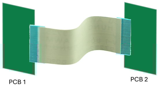 Figure 1. Picture of an FFC-based system.
 - Lines are the media inside the FFC used for signal transmission, which are made of good conductors.
It is important to emphasize the importance of crosstalk in the design of FFC cables. Crosstalk [1] occurs when the signal transmitted on a line interferes with signals on other adjacent lines, causing signal degradation and possible communication errors, such as attenuation or distortion of the signal to be transmitted, which can lead to encoding or decoding errors. This is particularly critical in high-frequency systems and especially in systems such as the FFC, where signals travel closely and parallel to each other, where even a small amount of noise can have a significant impact on the overall system performance.
Based on the aforementioned functional and performance goals, the objectives of this work can be summarized as follows. Given an FFC cable consisting of M lines transmitting N signals (with ), the goal is to optimize the arrangement of signals among the different lines to minimize interference related to the crosstalk phenomenon, meanwhile satisfying the need for the transmission of all N required signals.
3. Proposed Method
3.1. Linear Optimization Problems (LOPs)
Determining the optimal order of elements in a sequence of lines or paths is the goal of LOPs. There is no effective algorithm for solving these problems in polynomial time on a deterministic computer, so they are classified as NP-hard. This means that the complexity of these problems grows exponentially with the size of the input. Thus, the problem size is of order . Using advanced solving strategies such as heuristic algorithms, branch and bound algorithms, or linear or integer programming techniques is necessary because of the NP-hard complexity of LOP problems. However, even with these techniques, solving LOP problems can require a lot of computational power, particularly for large problems. To solve these types of problems, efficient exact algorithms could be developed for particular cases or limited input sizes. Once the evaluation method is developed, it is always possible to apply a brute force algorithm to find the optimal solution, that is, to vary all the parameters in order to obtain all possible combinations and a posteriori exclude the invalid ones. The process thus described, however, is always the least computationally efficient. The following constraints are therefore applied in the analysis: each signal can be transmitted only once, and only one signal can be transmitted per line. These constraints lead the problem back to a permutation. The number of valid combinations then reduces to
3.2. Optimization Problem
According to the theory [1], it is verified that the optimal condition is obtained when ground (GND) tracks can be interposed between the tracks crossed by critical signals. Such tracks define a path to ground for disturbances and thus provide effective shielding against crosstalk disturbances [12]. However, with the trend toward miniaturization and the decreasing footprint allocated for component placement, it becomes necessary to manage cases in which there is no availability of alternating ground tracks to the lines carrying critical signals, since all or nearly all lines are occupied by signals.
The proposed optimization makes it possible to determine the best arrangement of signals within the FFC, regardless of the number of GND traces available. The simulation-based optimization approach offers significant flexibility, allowing for the accommodation of a variety of constraints and design requirements. A computational model of a real system is then proposed to study its behavior and evaluate the effectiveness of different decision strategies. The structure under analysis is an FFC consisting of an M number of lines. The N signals to be transmitted will be modeled using appropriate generators as defined in the following sections. Figure 2 depicts the general structure of the proposed optimization technique that will be discussed in detail in the following subsections.
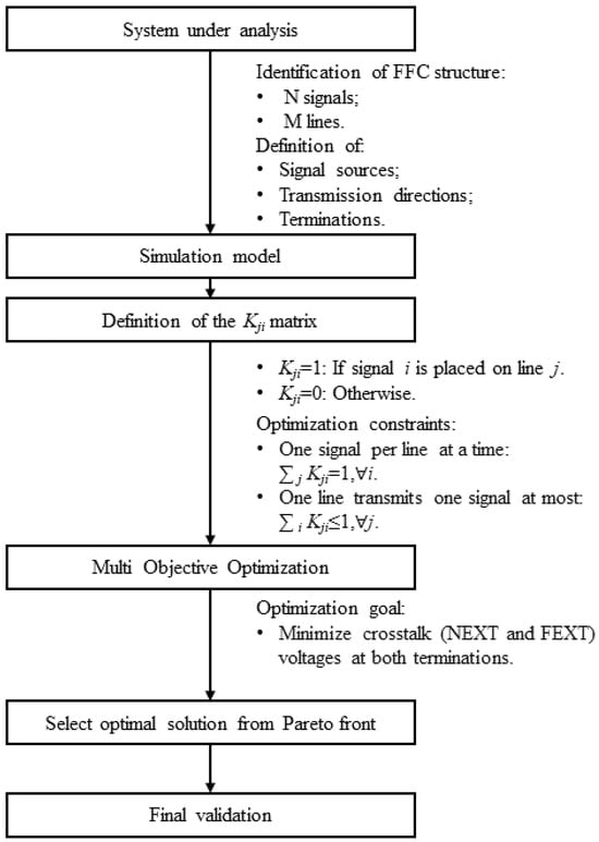
Figure 2.
Schematic diagram of the proposed optimization method.
3.2.1. Optimization Variables
To enable the passage in line j of the given signal i, dimensionless transfer coefficients are defined as (j = 1, …, M; i = 1, …, N). Schematically, we have the following:
- : if signal i is placed on line j;
- : otherwise.
An matrix is then defined that enables, according to combinatorial logic, the transmission of signals in the respective lines. Each line can transmit a signal in either direction, but this direction is settled as soon as the signal is determined. The enabled signals are then transmitted to the track terminations.
The transfer coefficients control the transmission properties dependent on the specific signal and the line, including the (a) placement of the signal source, (b) transmission direction, and (c) termination at both sides. Specifically, we have the following:
- (a)
- The placement of the signal source is mainly controlled in the model by ideal voltage-controlled voltage sources (VCVSs) as shown in Figure 3, where represents the signal i placed on line j. The gain of each VCVS varies discretely between 0 and 1. If the gain is 1, the signal i is transmitted through line j; conversely, if the gain is 0, the signal i does not pass through line j. Therefore, binary states are used to define the placement of signals without distortion or time delay. The use of ideal VCVSs ensures that the accuracy of the simulation remains unaffected, allowing for the precise analysis of delay and distortion solely introduced by the system under investigation.
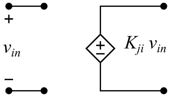 Figure 3. Voltage-controlled voltage source (VCVS). The gain varies discretely between 0 and 1.
 - (b)
- Transmission direction is controlled by using two separate sets of VCVSs, representing sources placed on the left or right sides and therefore controlling signal flow direction as will be illustrated in the following case study.
- (c)
- Termination: Lines that are not crossed by signals are terminated in open circuits (floating). Lines that are crossed by signals are terminated by the termination provided by the implemented standard. It is important to use proper terminations because it helps to ensure signal integrity during transmission through the communication medium. The value of terminations varies depending on the combination analyzed, so it varies with the state of the system. As a result, it is crucial to use a proper corresponding termination depending on the different signals and their transmission properties.
This assumption requires, in general, the termination circuit to be changed on time given a specific set of optimization variables. In the case study presented in the following section, an ad hoc method will be demonstrated to address this point, sorting the different terminations into two categories [15]:
- A high-impedance state that represents the input buffer behavior or no signal transmission behavior;
- A resistor of small value (nearly 33 ohm) that represents the output impedance related to a signal driver.
When a transfer coefficient is determined, the source and terminal impedance values are changed correspondingly to reflect the aforementioned point. This treatment simplifies the system implementation without compromising accuracy.
3.2.2. Optimization Constraints
Summarizing the requirements of signal transmission, the following constraints can be derived.
One signal is transmitted on one line at a time only:
One line transmits one signal at most:
3.2.3. Optimization Goal
Without loss of generality, in this work, the optimization goal is crosstalk minimization at both terminations, i.e., the simultaneous reduction in NEXT and FEXT phenomena, so MOO is opted for. Specifically, the electrical quantities that identify the NEXT and FEXT are the voltages at the beginning and end of the lines, respectively, as shown in Figure 4. More precisely, the voltages correspond to NEXT, while the voltages correspond to FEXT, for x ranging from 1 to M, and are expressed in V. Considering voltage crosstalk in the frequency domain, the functional waveform corresponds to the baseline of the voltage spectrum, and crosstalk contributes to the increased level of the spectrum. Therefore, in this work, the objective functions to be minimized are described by the total amount of voltage spectrum level as:
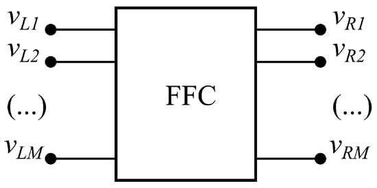
Figure 4.
Definition of voltages and that identify respectively NEXT and FEXT.
Here, the scalar quantities associated with the voltage amplitudes at the beginning and end of the line, i.e., at the left and right terminations of the line, respectively, are evaluated. The voltages are then first converted to the frequency domain. The maximum value for each waveform is selected and then the maximum peak between the latter values. For each of the states, (4) and (5) are computed. The results are presented in the form of a Pareto front. Using a Pareto front allows to clearly visualize the trade-offs between (4) and (5) and identify the solutions that offer the best performance. From the results, it will be possible to distinguish different classes and identify the best applicable designs.
Since the proposed method is general, in the practical case, objective functions can also be chosen to relate current expressions and/or time domain expressions, depending on the quantities of interest. It is also feasible to minimize the crosstalk only on a single (critical) side, thereby simplifying the problem, or to consider multiple (more than two) objective functions simultaneously by, for example, also taking into account the EMC performance indicators related to power integrity or radiated emissions, using a more generic MOO method as the optimization algorithm.
4. Discussion
4.1. Optimization Complexity and Heuristic Method
Following the aforementioned analysis, the studied issue becomes a binary optimization problem, where the state variable matrix with binary options needs to be decided. To automate the process of changing the termination value for each iteration, the termination value is defined through logical expressions. Several VCVSs are placed downstream of the terminations of each line to transmit signals, enabled when is equal to 1, to the terminations. These signals allow for crosstalk simulation.
Probes are then placed at the terminations to obtain the NEXT and FEXT trends evaluated at the left and right cable terminations, respectively. A minimal system is thus constructed to simulate the behavior in terms of SI. A heuristic algorithm is then developed to evaluate all valid combinations. Therefore, the following logic is followed for selecting the position of the signals with respect to the lines:
- Select line position of 1st signal (M choices);
- Select line position of 2nd signal ( choices);
- ...
- Select line position of Nth signal ( choices).
To be specific, for the implemented constraints, gains are selected with the following algorithm:
- One variable out of to (e.g., ) will be set to 1, the other variables with the same line number ( in this case) will be set to 0, and the other variables with the same signal number ( in this case) will be set to 0;
- In the submatrix formed by the remaining variables, one variable out of to (e.g., ) will be set to 1, the other variables with the same line number ( in this case) will be set to 0, and the other variables with the same signal number ( in this case) will be set to 0.
- And so on. A table of combinations is defined that includes all possible states of the system. This table is used to develop the parametric analysis. Once the parametric analysis part is defined, the optimization part is defined. An example of heuristic determination of transfer coefficients is shown in Figure 5, where variables in black are undetermined, variables in red are randomly chosen (i.e., independent variables), and variables in green are automatically determined (i.e., dependent variables) once the corresponding independent variables have been chosen.
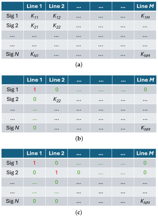 Figure 5. Heuristic determination of transfer coefficients considering the first two steps. (a) Initial state. (b) is randomly decided as 1, and elements in the same row and column are automatically determined as 0. (c) is randomly decided as 1, and elements in the same row and column are automatically determined as 0.
Following the above procedure, for a general M-line-N-signal system (with ), the total number of combinations is
4.2. Signal Transmission via Multiple Lines
Though the proposed method assumes that each signal is only transmitted once, it can be easily applied to the case where multiple lines are needed to transmit a specific signal, e.g., when the power signals are used (typically with DC voltage 3.3 V or 5 V) for powering up an auxiliary board connected to the main PCB. This can be performed by assigning different aliases to the same signal and duplicating the basic properties. For instance, if the power net named VDD is to be transmitted by two lines, two pseudo signals VDD1 and VDD2 can be set in the optimization problem, with each having the same direction and termination as VDD. Since the optimization is a separate procedure free from the PCB design, this does not affect the naming conventions or net information in PCB routing.
4.3. Various Interconnects Types
Finally, it is worth mentioning that the proposed method is generally applicable to the optimization of different systems of cables and interconnects as long as EMC performance is concerned, e.g., in designing the signal order of FPC, and combinations of FFC cables and connectors. This flexibility is due to the fact that the information of the system under analysis is simply the input for the proposed method as presented in Figure 2.
5. Case Study
To verify the validity of the proposed optimization method, standard Fast Ethernet communication working at 100 Mbit/s, which is widely used in modern smart electrical and electronic systems, is considered as a study case. Specifically, the analysis is targeted at optimizing the signal arrangement in an FFC used as an interconnection for communication with a Reduced Media Independent Interface (RMII) [16]. The schematic of the RMII signal is shown in Figure 6. This interface represents a typical form of communication signal transmission between different PCBs within a system and has several digital signals characterized by fast switching. The related EMC issues, such as SI and radiated emissions, can be crucial for such a system in a practical design.
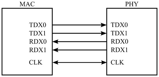
Figure 6.
Reduced Media Independent Interface (RMII) signal definition.
5.1. Reduced Media Independent Interface (RMII)
The RMII interface is an interface specification used primarily in network devices, particularly in Ethernet switches and local area network (LAN) switches, as well as in routers and other network devices. It represents an evolution of the Media Independent Interface (MII). This interface is designed to provide a connection between a network device processor and its Ethernet transceiver. The RMII interface is particularly beneficial for applications where space and power are limited, as it requires fewer pins than the standard MII interface and allows efficient connection between network devices. In terms of signals, the RMII interface comprises a number of high-speed digital signals, including data signals (TXD0 and TXD1 for transmission, RXD0 and RXD1 for reception), and a clock signal (CLK). In the RMII interface, the CLK signal is used to synchronize data transmission and reception between network devices and generally operates at a frequency of 50 MHz. As for the TXD0, TXD1, RXD0 and RXD1 signals, they are encoded using such techniques as MLT-3 or Manchester depending on the transmission rate of the implemented standard that allows the signal to be transmitted using a reduced bandwidth [17]. In this scenario, for the specifications of the signals to be simulated, the chosen standard is Ethernet 100BASE-TX.
The RMII interface is directly connected to the physical layer (PHY) of Ethernet, also known as the Ethernet physical layer, of the Open Systems Interconnection (OSI) model. This interface also communicates with layer 2 defined as Media Access Control (MAC), implemented via the Microcontroller Unit (MCU), which is responsible for functions such as MAC addressing, flow control, collision management, and the framing of data into packets or frames. The physical layer is responsible for the transmission of physical signals through the transmission medium, such as cables, fiber optics, or wireless. In newer, integrated implementations, both the MII interface and the Ethernet PHY can be integrated within the same Integrated Circuit (IC) chip or package. This approach offers advantages in terms of cost reduction, a more compact size, and reduced power consumption. Regarding the placement of OSI layer 1 and layer 2, there are applications where for reasons of footprint, mechanical design requirements, or system flexibility, it is preferred to separate the MCU and the Ethernet physical layer on two different boards. Taking this into consideration, an FFC may be the optimal solution to interconnect the two systems. It will then be necessary to define the optimal order of the signals described in order to reduce the possible electromagnetic interference between them. In order to reduce footprint space, it is also advisable to use connectors with a number of pins not exceeding the number of signals to be transmitted and, consequently, also cables with a reduced number of wires/traces.
5.2. Optimization Implementation
Let us consider an FFC consisting of six transmission lines as shown in Figure 7. The objective is to optimize the arrangement of the five signals CLK, TDX0, TXD1, RXD0 and RXD1 of the RMII interface. In the present case, therefore, N is equal to 5 and M is equal to 6. The voltages and , where x varies between 1 and 5, which define the crosstalk level for each line and are the objective of the subsequent optimization, are evaluated at the left and right ends of the line by means of appropriate scopes, positioned according to Figure 8.
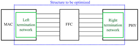
Figure 7.
Block diagram of the system under analysis. The structure undergoing optimization is highlighted. The number of lines that compose the FFC in this application is equal to six.
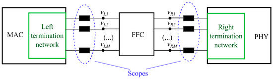
Figure 8.
Schematic of the studied system with optimization performance indicators monitored.
The FFC considered here is randomly selected from the market, considering the cable specifications given in [18]. Specifically, the geometric quantities are defined as follows (see Figure 9 and Figure 10): W = 3.5 mm; = 0.3 mm; = 0.5 mm; = = 0.045 mm; = 0.05 mm. The length L is varied for a more complete analysis. The cable electromagnetic simulation model is obtained by employing Ansys Q2D (version 2022R2) [19]. This choice is not exclusive; other software tools can be utilized as long as their integration with circuit simulation is feasible, given the general applicability of the proposed method.
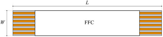
Figure 9.
FFC cable, top view. The width W and length L of the FFC are marked. Copper traces are shown in orange, while dielectric material is in gray.
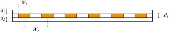
Figure 10.
FFC cross section. The six transmission lines are highlighted.
A specific direction of transmission is assumed for each signal (see Figure 6): the CLK and transmission signals are placed at the input to the left side of the cable, while the receiving signals are placed at the input to the right side of the cable. Specifically, we have the following:
- Modeling of signals: A clock generator with a frequency of 50 MHz is used to simulate the CLK signal. To simulate the transmission and reception signals, i.e., TDX0, TXD1, RXD0, and RXD1, independent signal generators that return a bit stream consistent with the communication standard specifications are used, requiring the use of a Pseudo Random Bit Sequence Generator (PRBS) in the circuit simulation. As represented in Figure 11, the transmission signals TDX0 and TXD1 are identified with the designation , the reception signals RXD0 and RXD1 are labeled as , and the clock signal CLK as .
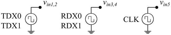 Figure 11. Definition of signal sources terminology applied to the case study.
 - Modeling of signal directions: The left and right termination networks are composed of six circuit branches, one for each signal line of the FFC. The individual left- and right-side circuit branches are shown in Figure 12 and Figure 13, respectively. The circuit branches thus described are used to simulate the crosstalk impacting the left and right terminations of the cable. The signals at the terminations are enabled through the VCVS depicted in Figure 3. The composition of the signals at the terminations is controlled by a second set of VCVSs as defined in Section 3.2.1. Dimensionless gains, with x varying between 1 and 5, are set equal to 1.
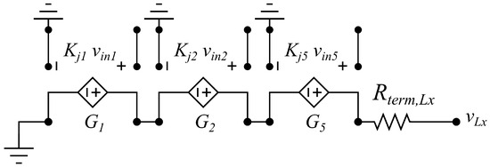 Figure 12. Scheme of a single branch of the left termination network in Figure 8. VCVS signals are enabled if the corresponding coefficient is equal to 1.
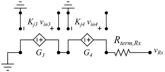 Figure 13. Scheme of a single branch of the right termination network in Figure 8. VCVS signals are enabled if the corresponding coefficient is equal to 1.
 - Modeling of terminations: As described in Section 3.2.1, the terminations of each line, namely and in Figure 12 and Figure 13 expressed in , can take one of two values, either open circuit or a specific resistance value depending on the requirements of the driver. For the RMII interface, the driver terminations commonly used and suggested by the design guidelines are 33 resistors. These resistors serve to maintain the integrity of signals during transmission through the communication medium, reducing the risk of reflections and ensuring that signals reach the receivers with optimal quality. The termination value is selected in an automated way through logic operations: if the transmission coefficient relative to line j is 1, the termination value of line j is set equal to 33 . Conversely, if is equal to 0, line j is terminated in high impedance. The selection of high impedance for idle lines is arbitrary. The results are not influenced by this choice.
The matrix allows exploring all possible combinations of the five signals transmitted by the six different lines. The total combinations and valid combinations [calculated using (6)] are shown in Table 1.

Table 1.
Computational complexity.
5.3. Results
The optimization results are then presented in the form of Pareto fronts. The optimization objective is to search for the order of signals that minimizes the functions (4) and (5), evaluated as described in Figure 8. When evaluating EMC performance, the effect of the signal order, the primary objective of the analysis, is explored, followed by the effect of the cable length.
5.3.1. Experiment 1: Effect of Signal Orders
The optimization described allows all valid combinations to be evaluated using the matrix. Different clusters are identified using the k-means clustering algorithm. In the first example, optimization is carried out by considering a cable length L = 1 cm. In this first case, the clusters are more defined, and it is possible to draw conclusions about the correct positioning of the signals easily. The results of this initial analysis are reported in Figure 14; each discrete value in the figure corresponds to a specific combination of . It is identified that the CLK signal is the most critical signal influencing the system EMC performance, and its proper arrangement can lead to the reduction in crosstalk. The best cases, identified by Cluster 2, in which, therefore, NEXT and FEXT are minimized, correspond to an arrangement of the CLK signal at either end of the group of lines in the cable (identified by lines 1 and 6). The worst cases in which NEXT and FEXT are maximized are identified by Cluster 1 and coincide with the CLK signal placed at the center of the tracks and interfaced to the transmission or reception signals. Specifically, in the best case, considering the minimized crosstalk, the CLK, which corresponds to the signal, is located on line 1, while in the worst case, it is located on line 3. This result indicates that the order of the signals has an impact on the EMC performance of the system. The analysis showed that choosing the order of the signals can reduce EMI without the need for substantial changes to the system architecture.
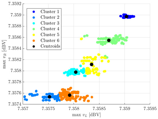
Figure 14.
Pareto front, obtained considering cm. The best solutions are identified by Cluster 2, the worst solutions are identified by Cluster 1.
5.3.2. Experiment 2: Effect of FFC Lengths
In the second experiment, optimization is carried out by considering three lengths L of the cable, i.e., 1 cm (see Figure 14), 5 cm (see Figure 15), and 10 cm (see Figure 16). In the previous example, though the clusters are clearly separated, the differences are very limited in scale. Comparing all three plots, when the cable length is longer, it is more clear that differences are predominant in the crosstalk voltages with different designs, though the clusters become vague. Indeed, since results are based on FFT of time-domain simulations and due to multiple reflections, the results with long FFC lengths are not easy to interpret. However, the obtained figures can still provide valuable information for the selection of the signal order. For instance, Figure 15 shows that Cluster 5 provides a trade-off solution with low-level crosstalk. In Figure 16, Clusters 3 and 2 offer extremely low NEXT and FEXT values but have relatively high FEXT and NEXT, respectively. In Figure 17, the impact of FEXT on the CLK signal is evaluated for the latter case, with cm. Here, the amplitude variations of the optimized quantities are larger and allow a better observation of the benefit gained from the optimization. The response of in the time domain is investigated. The red curve corresponds to when propagates along line 6, while the blue curve refers to when propagates along line 3. It is observed that placing the CLK in position 6 reduces signal oscillations compared to placing the same signal in position 3. Since the proposed method always searches for the optimal arrangement within the available range, with a longer length, the proposed method will be more beneficial in improving EMC performance.
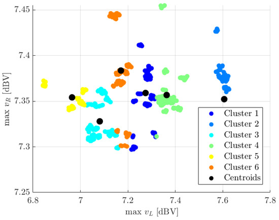
Figure 15.
Pareto front, obtained considering cm. The best solutions are identified by Cluster 5, and the worst solutions are identified by Cluster 2.
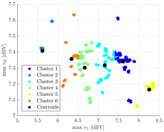
Figure 16.
Pareto front, obtained considering cm. In this case, defining the best and worst cases requires a thorough analysis of the results, which is not reported for brevity.
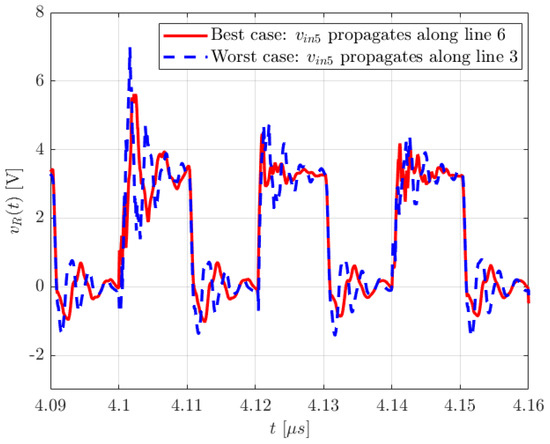
Figure 17.
Evaluation of FEXT impact on CLK signal ; the red curve represents considering propagating along line 6 (best case), the blue curve represents considering propagating along line 3 (worst case).
6. Conclusions
The paper describes an optimization procedure that provides a systematic approach to improving the EMC performance of FFCs. By optimizing the arrangement of signals within an FFC through a MOO approach, with the aim of minimizing NEXT and FEXT, this method improves the reliability and robustness of electrical and electronic systems. This optimization procedure is achieved by using some common circuit components, providing a easy-to-use optimization method for circuit designs. A case study focusing on optimizing signal organization for a RMII demonstrates the effectiveness of the proposed method. The results show that signal organization within an FFC significantly affects EMC performance, with proper signal ordering leading to reduced crosstalk and improved system reliability. A first analysis concerns the application of signal arrangement optimization within the FFC as defined in the first part of the paper. It is shown that there is an arrangement such that crosstalk is minimized. A second consideration is developed by considering different lengths of the FFC. Here, it is emphasized that as the length of the cable increases, it is even more important to optimize the arrangement. The difference in the magnitude of crosstalk between the best and worst solutions in fact increases, so deciding on a particular combination can lead to significant crosstalk optimization. In general, the proposed optimization method offers a cost-effective way to improve EMC performance in electrical and electronic systems without the need for major changes to the system architecture. By considering signal organization as a way to improve EMC performance, this method provides a valuable tool for system designers. Although the method in this instance is applied to the cable system alone, it is possible to extend the analysis by including connectors in the system, providing an optimization tailored to the particular configuration. Future works will involve incorporating complex multi-physics simulation models to assess the impact of environmental factors, such as temperature and humidity, on the EMC performance of the optimized FFC configuration, and the corresponding experimental validation.
Author Contributions
Conceptualization, L.I., X.L. and F.G.; methodology, L.I., X.L. and X.W.; software, L.I. and X.L.; validation, L.I. and X.L.; formal analysis, L.I., X.L. and X.W.; investigation, L.I.; resources, X.L., F.G. and S.A.P.; data curation, L.I.; writing—original draft preparation, L.I.; writing—review and editing, X.L., X.W., F.G. and S.A.P.; visualization, L.I.; supervision, X.L. and F.G.; project administration, F.G. and S.A.P.; funding acquisition, F.G. and S.A.P. All authors have read and agreed to the published version of the manuscript.
Funding
This research received no external funding.
Data Availability Statement
The original contributions presented in the study are included in the article, further inquiries can be directed to the corresponding authors.
Conflicts of Interest
The authors declare no conflicts of interest.
References
- Paul, C.R. Introduction to Electromagnetic Compatibility; John Wiley & Sons: Hoboken, NJ, USA, 2006. [Google Scholar]
- Illiano, L.; Wu, X.; Grassi, F.; Spadacini, G.; Pignari, S.A. Review of Mode Conversion and Modal Analysis in Electromagnetic Compatibility. IEEE Access 2024, 12, 65513–65529. [Google Scholar] [CrossRef]
- Wu, T.L.; Buesink, F.; Canavero, F. Overview of Signal Integrity and EMC Design Technologies on PCB: Fundamentals and Latest Progress. IEEE Trans. Electromagn. Compat. 2013, 55, 624–638. [Google Scholar] [CrossRef]
- Schiavinotto, T.; Stützle, T. The linear ordering problem: Instances, search space analysis and algorithms. J. Math. Model. Algorithms 2004, 3, 367–402. [Google Scholar] [CrossRef]
- Moiseev, K.; Kolodny, A.; Wimer, S. Interconnect Optimization by Net Ordering. In Multi-Net Optimization of VLSI Interconnect; Springer: New York, NY, USA, 2014; pp. 167–194. [Google Scholar]
- Wimer, S.; Moiseev, K.; Kolodny, A. On VLSI interconnect optimization and linear ordering problem. Optim. Eng. 2011, 12, 603–609. [Google Scholar] [CrossRef]
- Zhu, Z.M.; Hao, B.T.; En, Y.F.; Yang, Y.T.; Li, Y.J. An interconnecting bus power optimization method combining interconnect wire spacing with wire ordering. Chin. Phys. B 2011, 20, 068401. [Google Scholar] [CrossRef]
- Yan, X.; Wu, C.; Zhang, D.; Jin, S.; Wu, S.; Fan, J.; Hwang, C. EMI Investigation and Mitigation of Flexible Flat Cables and Connectors. In Proceedings of the 2021 IEEE International Joint EMC/SI/PI and EMC Europe Symposium, Raleigh, NC, USA, 26 July–13 August 2021; pp. 515–519. [Google Scholar] [CrossRef]
- Webb, D.P.; Jaggernauth, W.A.; Cottrill, M.W.C.; West, A.A.; Conway, P.P.; Palmer, P.J. Electromagnetic compatibility performance of large area flexible printed circuit automotive harness. Proc. Inst. Mech. Eng. Part J. Automob. Eng. 2004, 218, 667–673. [Google Scholar] [CrossRef]
- Silaghi, A.M.; Pescari, C.; Bleoju, C.; De Sabata, A. Solving Automotive Signal Integrity Issues by EMC Simulation. In Proceedings of the 2021 IEEE 27th International Symposium for Design and Technology in Electronic Packaging (SIITME), Timisoara, Romania, 27–30 October 2021; pp. 33–36. [Google Scholar] [CrossRef]
- Zwillich, V.; Menzel, W.; Roehrig, L.; Leier, H. Odd-mode impedance-controlled shielded flat flexible cables for in-vehicle data transmission. In Proceedings of the 2006 17th International Zurich Symposium on Electromagnetic Compatibility, Singapore, 27 February–3 March 2006; pp. 348–351. [Google Scholar] [CrossRef]
- Kim, J.; Yu, J.K.; Seol, B.S.; Lee, J.; Nah, W. High frequency signal transfer characteristic of a 40-pin FPC connector. In Proceedings of the 2008 8th International Symposium on Antennas, Propagation and EM Theory, Kunming, China, 2–5 November 2008; pp. 917–920. [Google Scholar]
- Huang, S.Y.; Huang, T.Y.; Liu, C.T.; Wu, R.B. Ringing noise suppression for differential signaling in unshielded flexible flat cable. IEEE Trans. Components Packag. Manuf. Technol. 2015, 5, 1152–1159. [Google Scholar] [CrossRef]
- Yang, X.; Zhou, D.; Song, W.; She, Y.; Chen, X. A Cable Layout Optimization Method for Electronic Systems Based on Ensemble Learning and Improved Differential Evolution Algorithm. IEEE Trans. Electromagn. Compat. 2021, 63, 1962–1971. [Google Scholar] [CrossRef]
- Simonovich, B. Driver’s Output Impedance from IBIS. Bert Simonovich’s Design Notes. 2022. Available online: https://blog.lamsimenterprises.com/2010/12/22/drivers-output-impedance-from-ibis/ (accessed on 24 April 2024).
- IEEE Std 802.3-2022; Revision of IEEE Std 802.3-2018. IEEE Standard for Ethernet. IEEE: Piscataway, NJ, USA, 2022. [CrossRef]
- Illiano, L.; Liu, X.; Wu, X.; Grassi, F.; Pignari, S.A. Circuit Modeling of Fast Ethernet Signal for EMC and SI Analysis. In Proceedings of the 2023 International Symposium on Electromagnetic Compatibility–EMC Europe, Krakow, Poland, 4–8 September 2023; pp. 1–6. [Google Scholar]
- Würth Elektronik. WR-FFC Flat Flexible Cable—687606050002. 2021. Available online: https://www.we-online.com/en/components/products/FFC_0_50_TYPE_1_6876XXXXX002 (accessed on 1 May 2024).
- ANSYS. Ansys Q3D Extractor: Multiphysics Parasitic Extraction & Analysis. 2024. Available online: https://www.ansys.com/products/electronics/ansys-q3d-extractor (accessed on 1 May 2024).
Disclaimer/Publisher’s Note: The statements, opinions and data contained in all publications are solely those of the individual author(s) and contributor(s) and not of MDPI and/or the editor(s). MDPI and/or the editor(s) disclaim responsibility for any injury to people or property resulting from any ideas, methods, instructions or products referred to in the content. |
© 2024 by the authors. Licensee MDPI, Basel, Switzerland. This article is an open access article distributed under the terms and conditions of the Creative Commons Attribution (CC BY) license (https://creativecommons.org/licenses/by/4.0/).