
Switched Capacitor Inverter with Reduced Inrush Current and High Boosting Gain

Abstract
:1. Introduction
- The suggested architecture has a lesser number of components: one DC source, three diodes, and thirteen switches;
- The proposed topology possesses voltage-boosting capability;
- A voltage sensor circuit is not needed because the capacitors’ voltage is self-balancing;
- LS-SPWM control logic (i.e., complementary switching pair for pulse creation) is developed;
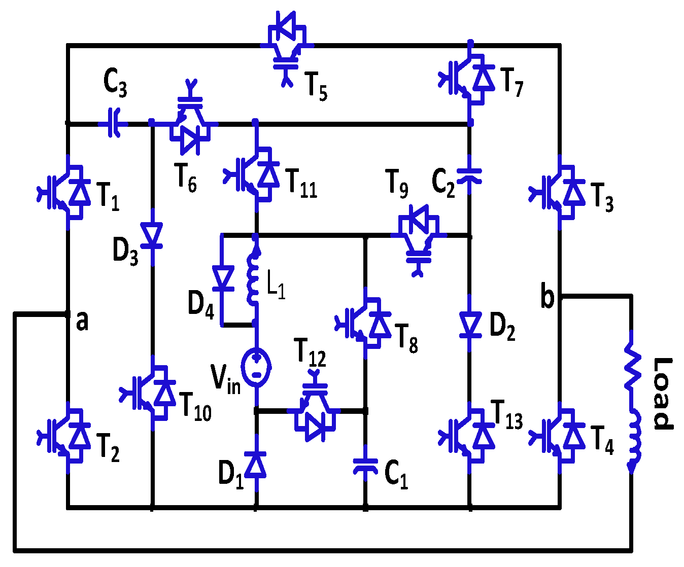
- The topology with a charging inductor and diode reduces capacitor inrush current to a great extent;
- The topology is cost effective and can be used for medium-to-high-power applications.
2. Proposed Switched Capacitor Topology
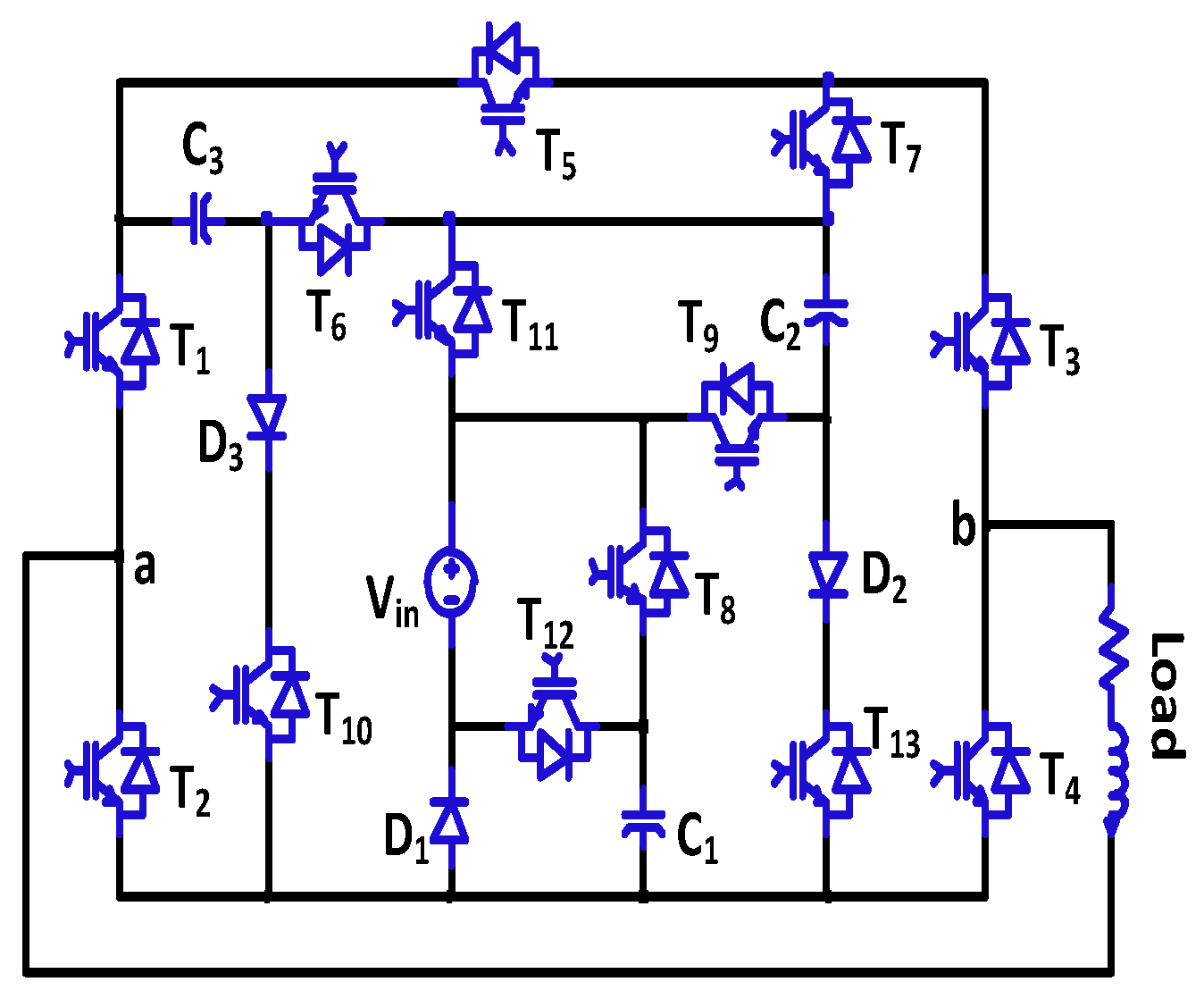
2.1. Operation
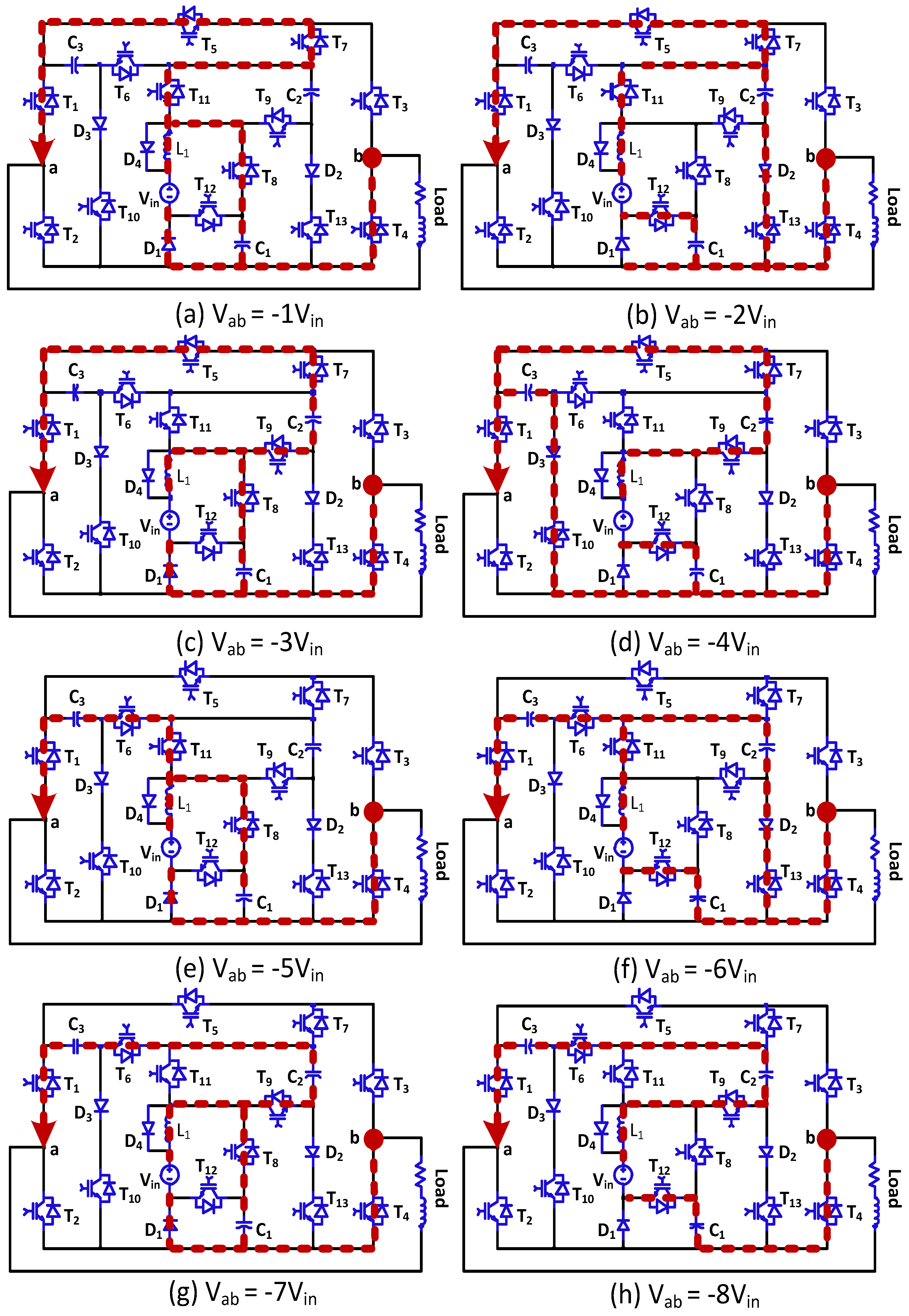
2.1.1. Step P1
2.1.2. Step P2
2.1.3. Step P3
2.1.4. Step P4
2.1.5. Step P5
2.1.6. Step P6
2.1.7. Step P7
2.1.8. Step P8
2.1.9. Step N1
2.1.10. Step N2
2.1.11. Step N3
2.1.12. Step N4
2.1.13. Step N5
2.1.14. Step N6
2.1.15. Step N7
2.1.16. Step N8
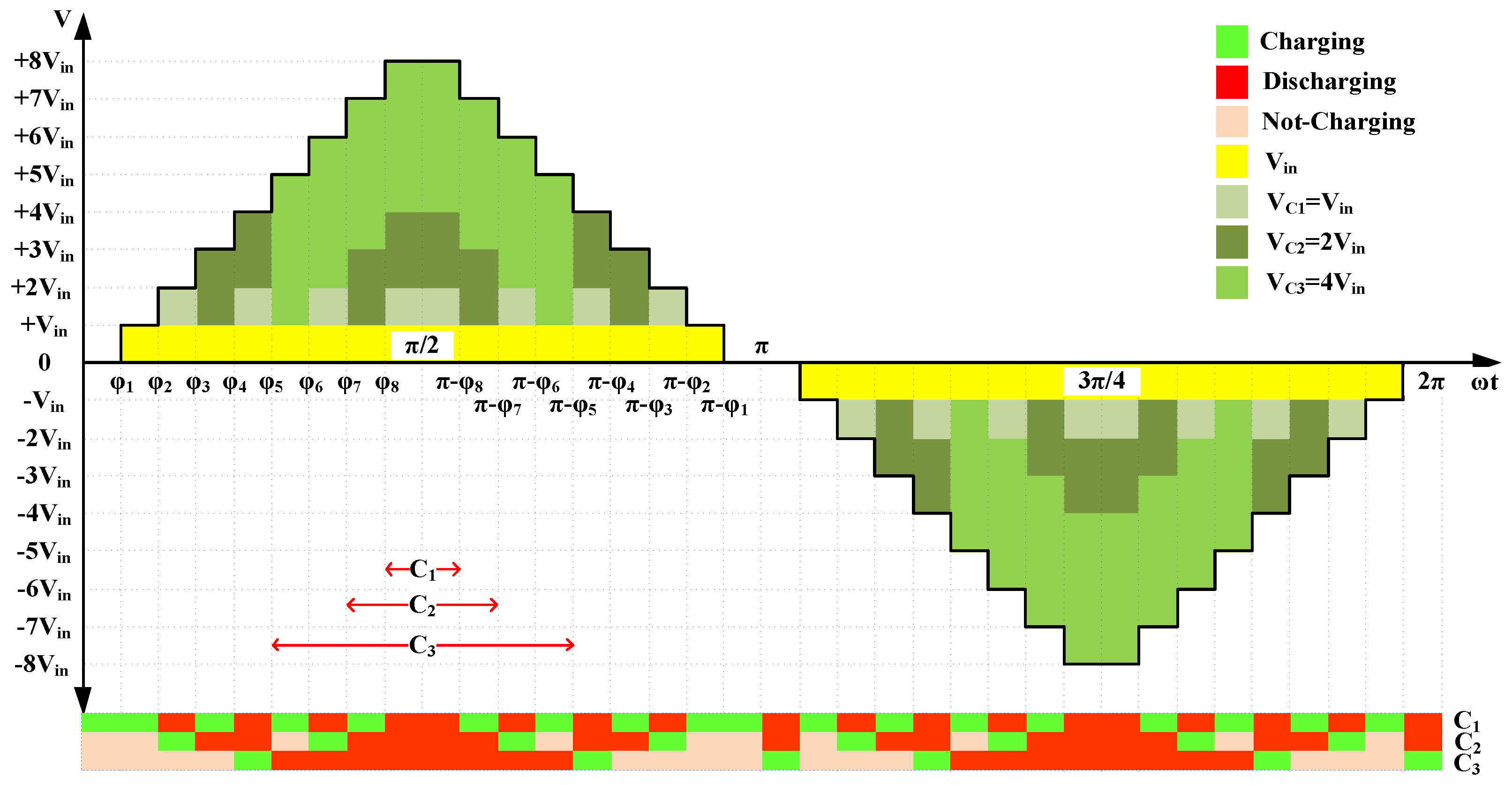
2.2. Maximum Blocking Voltage (MBV)
2.3. Modulation Scheme
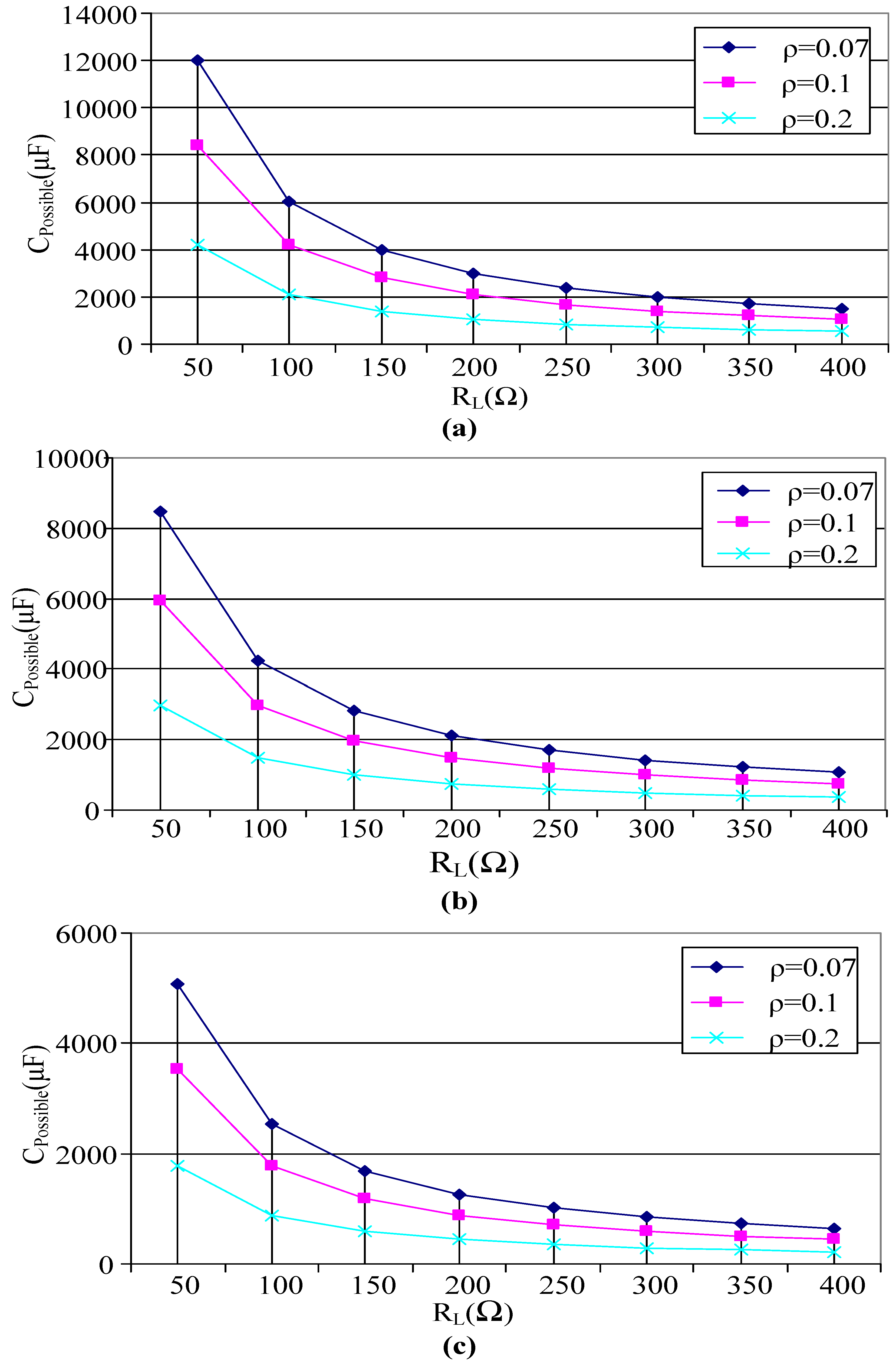
2.4. Selection of Capacitor
2.5. Selection of Optimal Value of Inductor
2.6. Power Loss
2.6.1. Conduction Loss
2.6.2. Switching Loss
2.6.3. Capacitor Equivalent Series Resistance Loss

| PSw. | PCon. | PTotal | |
|---|---|---|---|
| T1 | 0.5871 | 1.304 | 1.887 |
| T2 | 0.46 | 1.40 | 1.86 |
| T3 | 0.23792 | 1.2167 | 1.44 |
| T4 | 0.3472 | 1.237 | 1.57 |
| T5 | 0.3572 | 1.1171 | 1.41 |
| T6 | 0.4572 | 1.07 | 1.429 |
| T7 | 0.25 | 0.67 | 0.92 |
| T8 | 0.11 | 0.35 | 0.46 |
| T9 | 0.258 | 0.4788 | 0.43 |
| T10 | 0.27 | 0.35 | 0.62 |
| T11 | 0.112 | 0.226 | 0.33 |
| T12 | 0.107 | 0.223 | 0.32 |
| T13 | 0.1018 | 0.223 | 0.325 |
| D1 | 2.538 | ||
| D2 | 1.2 | ||
| D3 | 1.06 | ||
| D4 | 0.7120 | ||
| C1 | 0.812 | ||
| C2 | 1.34 | ||
| C3 | 2.164 | ||
| Total losses | 23.79 | ||
| Rated power = 610 W | 610 | ||
| (%) | 96.13 |

3. Comparison
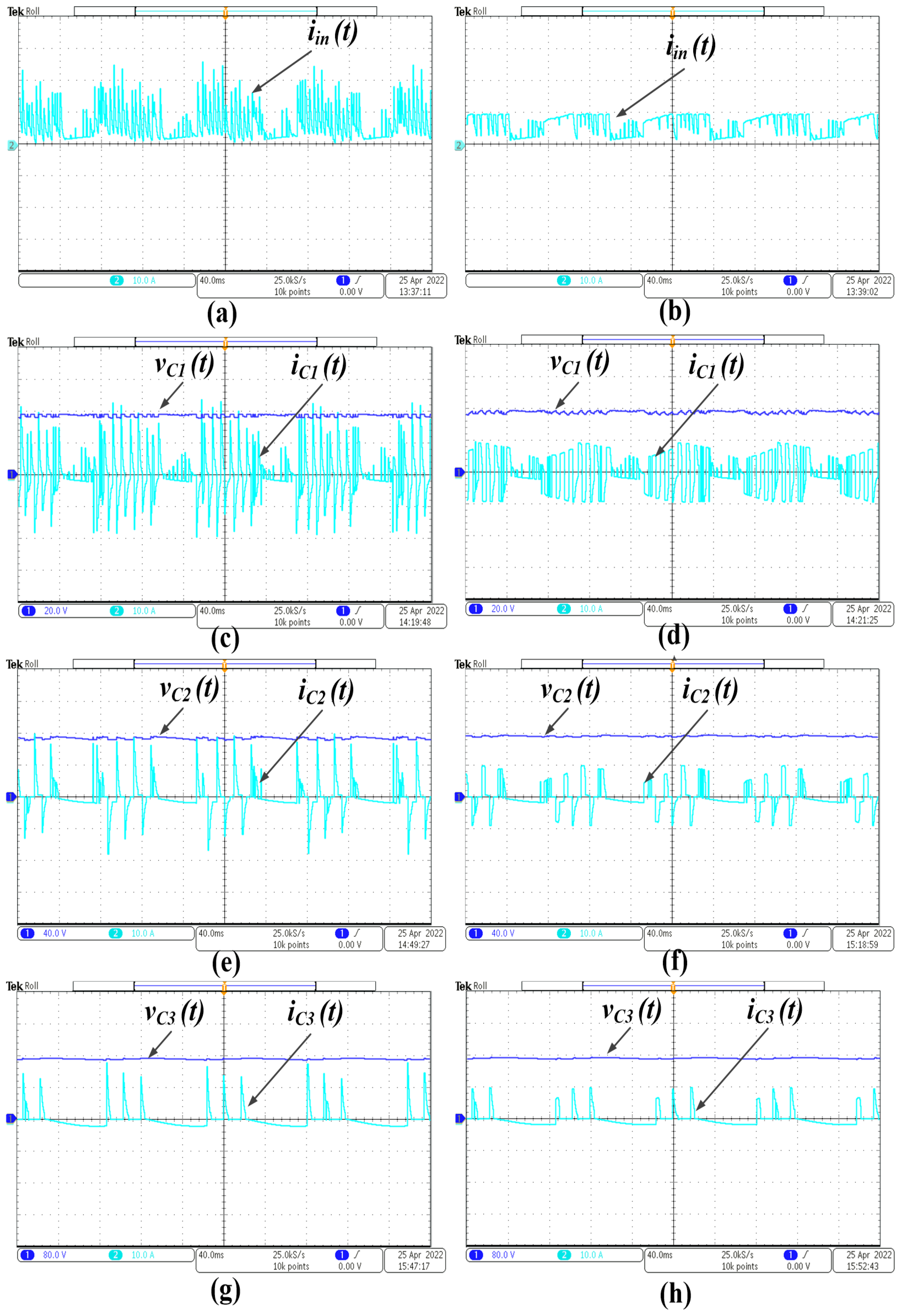
4. Experimental Setup and Results

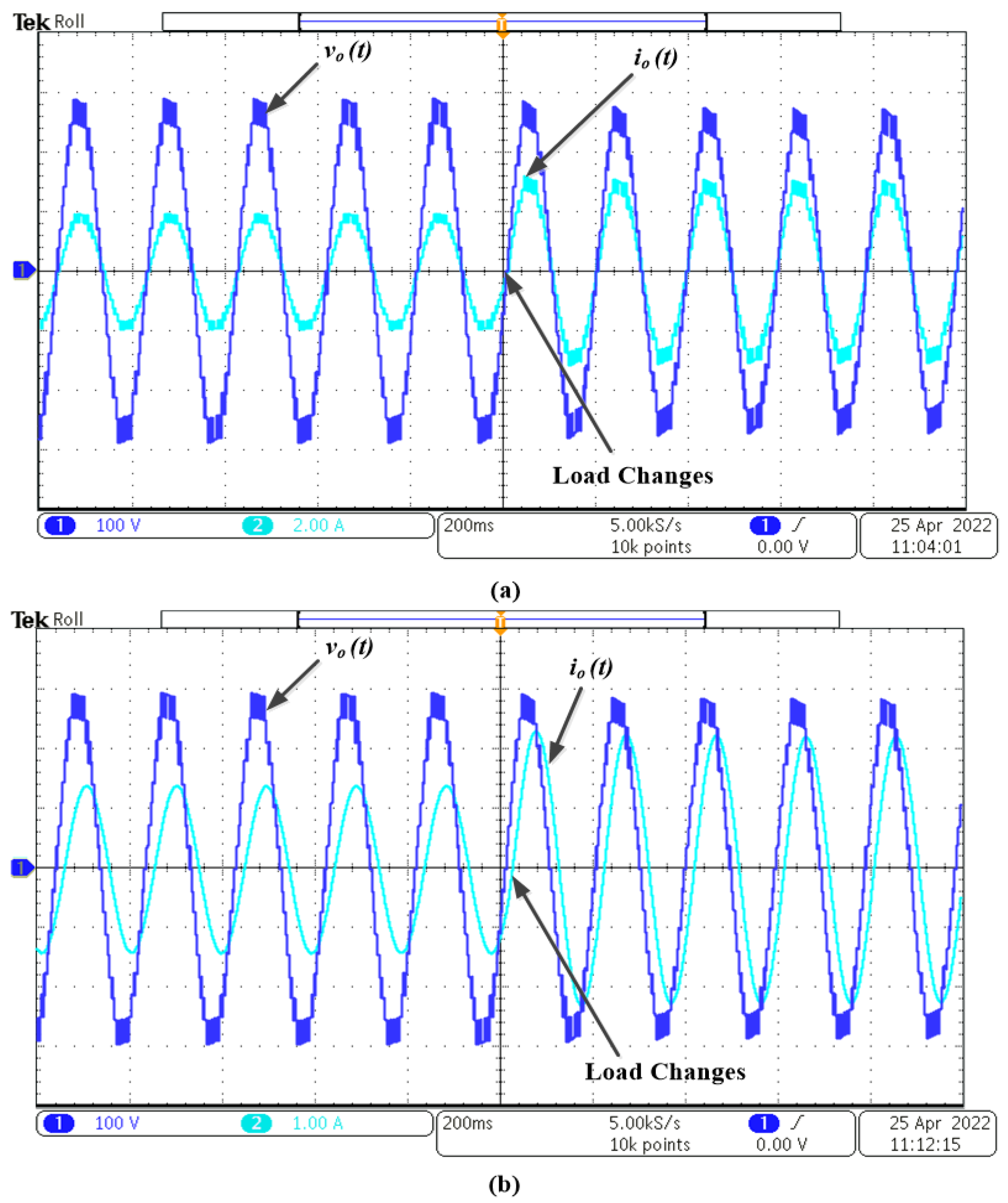

| Parameters | Rating |
|---|---|
| Vin | 40 V to 30 V |
| fc | 5 kHz |
| 140 Ω | |
| 80 Ω | |
| 140 Ω + 300 mH | |
| 80 Ω + 200 mH | |
| 1000 μF, 1500 μF, 2200 μF | |
| Charging inductor () | 58 μH |
| Delay time | 2 μs |
| Switches | CT60AM18F |
| Optocoupler | TLP250 |
| Modulation index | 0.55 to 0.99 |
5. Conclusions
Author Contributions
Funding
Data Availability Statement
Conflicts of Interest
References
- Jain, P.; Tanju, M. Improved DC/AC interface inverter for high-frequency space applications. IEEE Trans. Aerosp. Electron. Syst. 1993, 29, 1150–1163. [Google Scholar] [CrossRef]
- Behbahanifard, H.; Abazari, S.; Sadoughi, A. New scheme of SHE-PWM technique for cascaded multilevel inverters with regulation of DC voltage sources. ISA Trans. 2020, 97, 44–52. [Google Scholar] [CrossRef] [PubMed]
- Abu-Rub, H.; Lewicki, A.; Iqbal, A.; Guzinski, J. Medium voltage drives-challenges and requirements. In Proceedings of the 2010 IEEE International Symposium on Industrial Electronics, Bari, Italy, 4–7 July 2010; pp. 1372–1377. [Google Scholar]
- Le, Q.A.; Lee, D.C. A Novel Six-Level Inverter Topology for Medium-Voltage Applications. IEEE Trans. Ind. Electron. 2016, 63, 7195–7203. [Google Scholar] [CrossRef]
- Fathi, H.; Madadi, H. Enhanced-Boost Z-Source Inverters with Switched Z-Impedance. IEEE Trans. Ind. Electron. 2016, 63, 691–703. [Google Scholar] [CrossRef]
- Errabelli, R.R.; Mutschler, P. Fault-Tolerant Voltage Source Inverter for Permanent Magnet Drives. IEEE Trans. Power Electron. 2012, 27, 500–508. [Google Scholar] [CrossRef]
- Appelbaumior, J.; Gabbaymber, D. Stepped Sinewave Inverter. IEEE Trans. Aerosp. Electron. Syst. 1984, AES-20, 754–760. [Google Scholar] [CrossRef]
- Abu-Rub, H.; Holtz, J.; Rodriguez, J.; Baoming, G. Medium-Voltage Multilevel Converters—State of the Art, Challenges, and Requirements in Industrial Applications. IEEE Trans. Ind. Electron. 2010, 57, 2581–2596. [Google Scholar] [CrossRef]
- Kumari, M.; Siddique, M.D.; Sarwar, A.; Tariq, M.; Mekhilef, S.; Iqbal, A. Recent trends and review on switched-capacitor-based single-stage boost multilevel inverter. Int. Trans. Electr. Energy Syst. 2021, 31, e12730. [Google Scholar] [CrossRef]
- Priya, M.; Ponnambalam, P.; Muralikumar, K. Modular-multilevel converter topologies and applications—A review. IET Power Electron. 2019, 12, 170–183. [Google Scholar] [CrossRef]
- Memon, M.; Mekhilef, S.; Mubin, M.; Aamir, M. Selective harmonic elimination in inverters using bio-inspired intelligent algorithms for renewable energy conversion applications: A review. Renew. Sustain. Energy Rev. 2018, 82, 2235–2253. [Google Scholar] [CrossRef]
- Siahbalaee, J.; Sanaie, N. Comparison of conventional and new cascaded multilevel inverter topologies based on novel indices. ISA Trans. 2021, 119, 41–51. [Google Scholar] [CrossRef] [PubMed]
- Samsami, H.; Taheri, A.; Samanbakhsh, R. New bidirectional multilevel inverter topology with staircase cascading for symmetric and asymmetric structures. IET Power Electron. 2017, 10, 1315–1323. [Google Scholar] [CrossRef]
- Samadaei, E.; Gholamian, S.A.; Sheikholeslami, A.; Adabi, J. An Envelope Type (E-Type) Module: Asymmetric Multilevel Inverters With Reduced Components. IEEE Trans. Ind. Electron. 2016, 63, 7148–7156. [Google Scholar] [CrossRef]
- Samadaei, E.; Sheikholeslami, A.; Gholamian, S.A.; Adabi, J. A Square T-Type (ST-Type) Module for Asymmetrical Multilevel Inverters. IEEE Trans. Power Electron. 2018, 33, 987–996. [Google Scholar] [CrossRef]
- Alishah, R.S.; Hosseini, S.H.; Babaei, E.; Sabahi, M. Optimal Design of New Cascaded Switch-Ladder Multilevel Inverter Structure. IEEE Trans. Ind. Electron. 2017, 64, 2072–2080. [Google Scholar] [CrossRef]
- Karimi, M.; Kargar, P.; Varesi, K. An extendable asymmetric boost multi-level inverter with self-balanced capacitors. Int. J. Circuit Theory Appl. 2022, 50, 1297–1316. [Google Scholar] [CrossRef]
- Alishah, R.S.; Hosseini, S.H.; Babaei, E.; Sabahi, M. A New General Multilevel Converter Topology Based on Cascaded Connection of Submultilevel Units With Reduced Switching Components, DC Sources, and Blocked Voltage by Switches. IEEE Trans. Ind. Electron. 2016, 63, 7157–7164. [Google Scholar] [CrossRef]
- Babaei, E.; Sarbanzadeh, M.; Hosseinzadeh, M.A.; Cecati, C. A new basic unit for symmetric and asymmetric cascaded multilevel inverter with reduced number of components. In Proceedings of the IECON 2016—42nd Annual Conference of the IEEE Industrial Electronics Society, Florence, Italy, 24–27 October 2016; pp. 3147–3152. [Google Scholar] [CrossRef]
- Gharehkoushan, A.; Babaei, E.; Alishah, R.; Sabahi, M.; Hosseini, H. Optimal Design of New Cascade Multilevel Converter Topology Based on Series Connection of Extended Sub-multilevel Units. IET Power Electron. 2016, 9, 1341–1349. [Google Scholar] [CrossRef]
- Shalchi Alishah, R.; Nazarpour, D.; Hosseini, S.H.; Sabahi, M. Novel Topologies for Symmetric, Asymmetric, and Cascade Switched-Diode Multilevel Converter with Minimum Number of Power Electronic Components. IEEE Trans. Ind. Electron. 2014, 61, 5300–5310. [Google Scholar] [CrossRef]
- Babaei, E.; Laali, S. Optimum Structures of Proposed New Cascaded Multilevel Inverter with Reduced Number of Components. IEEE Trans. Ind. Electron. 2015, 62, 6887–6895. [Google Scholar] [CrossRef]
- Shalchi Alishah, R.; Nazarpour, D.; Hosseini, S.H.; Sabahi, M. Reduction of Power Electronic Elements in Multilevel Converters Using a New Cascade Structure. IEEE Trans. Ind. Electron. 2015, 62, 256–269. [Google Scholar] [CrossRef]
- Bana, P.R.; Panda, K.P.; Panda, G. Power Quality Performance Evaluation of Multilevel Inverter with Reduced Switching Devices and Minimum Standing Voltage. IEEE Trans. Ind. Inform. 2020, 16, 5009–5022. [Google Scholar] [CrossRef]
- Singh, D.; Sandeep, N. Switched-Capacitor-Based Multi-Source Multilevel Inverter with Reduced Part Count. IEEE J. Emerg. Sel. Top. Ind. Electron. 2023, 4, 718–724. [Google Scholar] [CrossRef]
- Islam, S.; Siddique, M.D.; Iqbal, A.; Mekhilef, S.; Al-Hitmi, M. A Switched Capacitor-Based 13-Level Inverter with Reduced Switch Count. IEEE Trans. Ind. Appl. 2022, 58, 7373–7383. [Google Scholar] [CrossRef]
- Siddique, M.D.; Karim, M.F.; Mekhilef, S.; Rawa, M.; Seyedmahmoudian, M.; Horan, B.; Stojcevski, A.; Ahmed, M. Single-Phase Boost Switched-Capacitor-Based Multilevel Inverter Topology with Reduced Switching Devices. IEEE J. Emerg. Sel. Top. Power Electron. 2022, 10, 4336–4346. [Google Scholar] [CrossRef]
- Bhatnagar, P.; Singh, A.K.; Gupta, K.K.; Siwakoti, Y.P. A Switched-Capacitors-Based 13-Level Inverter. IEEE Trans. Power Electron. 2022, 37, 644–658. [Google Scholar] [CrossRef]
- Singh, A.K.; Mandal, R.K. A Novel 17-Level Reduced Component Single DC Switched-Capacitor-Based Inverter with Reduced Input Spike Current. IEEE J. Emerg. Sel. Top. Power Electron. 2022, 10, 6045–6056. [Google Scholar] [CrossRef]
- Anand, V.; Singh, V.; Guo, X.; Sathik, M.A.J.; Siwakoti, Y.P.; Mekhilef, S.; Blaabjerg, F. Seventeen Level Switched Capacitor Inverters With the Capability of High Voltage Gain and Low Inrush Current. IEEE J. Emerg. Sel. Top. Ind. Electron. 2023, 4, 1138–1150. [Google Scholar] [CrossRef]
- Panda, K.P.; Naayagi, R.; Ray, P.K.; Panda, G. Single-source Switched-capacitor Boost Nine-level Inverter with Reduced Components. CSEE J. Power Energy Syst. 2023, 9, 1688–1697. [Google Scholar] [CrossRef]
- Wang, Y.; Wang, K.; Li, G.; Wu, F.; Wang, K.; Liang, J. Generalized Switched-Capacitor Step-up Multilevel Inverter Employing Single DC Source. CSEE J. Power Energy Syst. 2022, 8, 439–451. [Google Scholar] [CrossRef]
- Majumdar, S.; Jana, K.C.; Pal, P.K.; Sangwongwanich, A.; Blaabjerg, F. Design and Implementation of a Single-Source 17-Level Inverter for a Single-Phase Transformer-Less Grid-Connected Photovoltaic Systems. IEEE J. Emerg. Sel. Top. Power Electron. 2022, 10, 4469–4485. [Google Scholar] [CrossRef]
- Júnior, S.C.S.; Jacobina, C.B.; Fabricio, E.L.L.; Felinto, A.S. Asymmetric 49-Levels Cascaded MPUC Multilevel Inverter Fed by a Single DC Source. IEEE Trans. Ind. Appl. 2022, 58, 7539–7549. [Google Scholar] [CrossRef]
- Ali, J.S.A.; Almakhles, D.J.; Elmorshedy, M.F. High Boost Seventeen-Level Switched Capacitor Inverter Topology with Continuous Input Current. IEEE J. Emerg. Sel. Top. Power Electron. 2023, 11, 2742–2754. [Google Scholar] [CrossRef]
- Sandeep, N. A 13-Level Switched-Capacitor-Based Boosting Inverter. IEEE Trans. Circuits Syst. II Express Briefs 2021, 68, 998–1002. [Google Scholar] [CrossRef]
- Mohamed Ali, J.S.; Almakhles, D.; Sandeep, N.; Daula Siddique, M. Experimental validation of new self-voltage balanced 9L-ANPC inverter for photovoltaic applications. Sci. Rep. 2021, 11, 5067. [Google Scholar] [CrossRef] [PubMed]
- Khoun Jahan, H.; Abapour, M.; Zare, K. Switched-Capacitor-Based Single-Source Cascaded H-Bridge Multilevel Inverter Featuring Boosting Ability. IEEE Trans. Power Electron. 2019, 34, 1113–1124. [Google Scholar] [CrossRef]
- Siddique, M.D.; Mekhilef, S.; Shah, N.M.; Sarwar, A.; Iqbal, A.; Tayyab, M.; Ansari, M.K. Low Switching Frequency Based Asymmetrical Multilevel Inverter Topology With Reduced Switch Count. IEEE Access 2019, 7, 86374–86383. [Google Scholar] [CrossRef]
- Orfanoudakis, G.I.; Sharkh, S.M.; Yuratich, M.A. Analysis of DC-Link capacitor losses in three-level neutral point clamped and cascaded H-Bridge voltage source inverters. In Proceedings of the 2010 IEEE International Symposium on Industrial Electronics, Bari, Italy, 4–7 July 2010; pp. 664–669. [Google Scholar] [CrossRef]
- Barzegarkhoo, R.; Kojabadi, H.M.; Zamiry, E.; Vosoughi, N.; Chang, L. Generalized Structure for a Single Phase Switched-Capacitor Multilevel Inverter Using a New Multiple DC Link Producer with Reduced Number of Switches. IEEE Trans. Power Electron. 2016, 31, 5604–5617. [Google Scholar] [CrossRef]
- Zamiri, E.; Vosoughi, N.; Hosseini, S.H.; Barzegarkhoo, R.; Sabahi, M. A New Cascaded Switched-Capacitor Multilevel Inverter Based on Improved Series–Parallel Conversion with Less Number of Components. IEEE Trans. Ind. Electron. 2016, 63, 3582–3594. [Google Scholar] [CrossRef]
- Shalchi Alishah, R.; Hosseini, S.H.; Babaei, E.; Sabahi, M. Optimization Assessment of a New Extended Multilevel Converter Topology. IEEE Trans. Ind. Electron. 2017, 64, 4530–4538. [Google Scholar] [CrossRef]
- Barzegarkhoo, R.; Moradzadeh, M.; Zamiri, E.; Madadi Kojabadi, H.; Blaabjerg, F. A New Boost Switched-Capacitor Multilevel Converter With Reduced Circuit Devices. IEEE Trans. Power Electron. 2018, 33, 6738–6754. [Google Scholar] [CrossRef]
- Dhanamjayulu, C.; Meikandasivam, S. Implementation and Comparison of Symmetric and Asymmetric Multilevel Inverters for Dynamic Loads. IEEE Access 2018, 6, 738–746. [Google Scholar] [CrossRef]
- Lee, S.S. Single-Stage Switched-Capacitor Module (S3CM) Topology for Cascaded Multilevel Inverter. IEEE Trans. Power Electron. 2018, 33, 8204–8207. [Google Scholar] [CrossRef]
- Taghvaie, A.; Adabi, J.; Rezanejad, M. A Self-Balanced Step-Up Multilevel Inverter Based on Switched-Capacitor Structure. IEEE Trans. Power Electron. 2018, 33, 199–209. [Google Scholar] [CrossRef]
- Sathik Mohamed Ali, J.; Shalchi Alishah, R.; Sandeep, N.; Hosseini, S.H.; Babaei, E.; Vijayakumar, K.; Yaragatti, U.R. A New Generalized Multilevel Converter Topology Based on Cascaded Connection of Basic Units. IEEE J. Emerg. Sel. Top. Power Electron. 2019, 7, 2498–2512. [Google Scholar] [CrossRef]
- Hamidi, M.N.; Ishak, D.; Zainuri, M.A.A.M.; Ooi, C.A. Multilevel inverter with improved basic unit structure for symmetric and asymmetric source configuration. IET Power Electron. 2020, 13, 1445–1455. [Google Scholar] [CrossRef]
- Dhanamjayulu, C.; Prasad, D.; Padmanaban, S.; Maroti, P.K.; Holm-Nielsen, J.B.; Blaabjerg, F. Design and Implementation of Seventeen Level Inverter with Reduced Components. IEEE Access 2021, 9, 16746–16760. [Google Scholar] [CrossRef]
- Al-Hitmi, M.A.; Hussan, M.R.; Iqbal, A.; Islam, S. Symmetric and Asymmetric Multilevel Inverter Topologies with Reduced Device Count. IEEE Access 2023, 11, 5231–5245. [Google Scholar] [CrossRef]
- Marangalu, M.; Vosoughi kurdkandi, N.; Hosseini, S.H.; Tarzamni, H.; Dahidah, M.; Sarhangzadeh, M. A Modified Switched-Capacitor Based Seventeen-Level Inverter with Reduced Capacitor Charging Spike for RES Applications. IEEE Open J. Power Electron. 2023, 4, 579–602. [Google Scholar] [CrossRef]
- Hosseinpour, M.; Derakhshandeh, M.; Seifi, A.; Shahparasti, M. A 17-level quadruple boost switched-capacitor inverter with reduced devices and limited charge current. Sci. Rep. 2024, 14, 6233. [Google Scholar] [CrossRef] [PubMed]
- Ye, Y.; Chen, S.; Hua, T.; Lin, M.; Wang, X. Self-Balanced Multilevel Inverter With Hybrid Double- and Half-Mode Switched Capacitor. IEEE Trans. Ind. Electron. 2022, 69, 5735–5744. [Google Scholar] [CrossRef]
- Roy, T.; Sadhu, P.K. A Step-Up Multilevel Inverter Topology Using Novel Switched Capacitor Converters with Reduced Components. IEEE Trans. Ind. Electron. 2021, 68, 236–247. [Google Scholar] [CrossRef]

| Switches | Diodes | Capacitors | |||
|---|---|---|---|---|---|
| , , , , , and | − | ⇓ | ⇓ | ⇓ | |
| , , , , , and | ⇑ | ⇓ | ⇓ | ||
| , , , , , , and | ⇓ | ⇑ | ⇓ | ||
| , , , , , and | ⇑ | ¬ | ⇓ | ||
| , , , , , , and | ⇓ | ⇓ | ⇑ | ||
| , , , , and | ⇑ | ⇓ | ¬ | ||
| , , , , , and | ⇓ | ⇑ | ¬ | ||
| , , , , and | ⇑ | ¬ | ¬ | ||
| , , and | - | ¬ | ¬ | ¬ | 0 |
| and | - | ¬ | ¬ | ¬ | 0 |
| , , , , , and | ⇑ | ¬ | ¬ | ||
| , , , , , , and | ⇓ | ⇑ | ¬ | ||
| , , , , , and | ⇑ | ⇓ | ¬ | ||
| , , , , , , and | ⇓ | ⇓ | ⇑ | ||
| , , , , and | ⇑ | ¬ | ⇓ | ||
| , , , , , and | ⇓ | ⇑ | ⇓ | ||
| , , , , and | ⇑ | ⇓ | ⇓ | ||
| , , , , and | − | ⇓ | ⇓ | ⇓ | |
| Ci,min (F) | R = 140 Ω; L = 0 mH | R = 80 Ω; L = 300 mH | ||||
|---|---|---|---|---|---|---|
| C1,min | 1808.45 | 1265.9 | 632.96 | 1325.34 | 927.73 | 463.87 |
| C2,min | 3029.59 | 2120.70 | 1060.40 | 2220.26 | 1554.18 | 777.09 |
| C3,min | 4296.78 | 3007.75 | 1503.88 | 3148.93 | 2204.25 | 1102.13 |
| Topology | Nlevel | NDC | Nsw | Ndio | Ncap | G | TSV | TSVpu | CF/Nlevel | Voltage THD | |
|---|---|---|---|---|---|---|---|---|---|---|---|
| (%) | |||||||||||
| [18] | 17 | 4 | 12 | 0 | 0 | 1 | 44 | 44 | 10.82 | 21.18 | - |
| [41] | 17 | 1 | 24 | 8 | 7 | 8 | 72 | 9 | 3.97 | 4.5 | 4.5 |
| [20] | 17 | 4 | 10 | 0 | 0 | 1 | 40 | 40 | 9.41 | 18.82 | 4.38 |
| [42] | 17 | 4 | 20 | 4 | 4 | 4 | 60 | 20 | 13.64 | 18.35 | - |
| [16] | 17 | 4 | 10 | 0 | 0 | 1 | 38 | 38 | 9.18 | 18.12 | - |
| [43] | 17 | 4 | 10 | 0 | 0 | 1 | 38 | 38 | 9.18 | 18.12 | - |
| [15] | 17 | 4 | 12 | 0 | 0 | 1 | 48 | 48 | 11.3 | 22.56 | 2.77 |
| [44] | 17 | 2 | 18 | 2 | 4 | 4 | 24 | 6 | 5.29 | 6 | - |
| [45] | 17 | 8 | 20 | 16 | 0 | 1 | 40 | 40 | 35.76 | 54.59 | 5.41 |
| [46] | 17 | 2 | 24 | 0 | 4 | 2 | 24 | 12 | 6.8 | 8.2 | - |
| [47] | 17 | 1 | 39 | 0 | 7 | 8 | 39 | 4.875 | 5.14 | 5.43 | - |
| [48] | 17 | 4 | 10 | 0 | 0 | 1 | 36 | 36 | 8.94 | 17.41 | 6.17 |
| [49] | 17 | 4 | 20 | 0 | 0 | 1 | 40 | 40 | 14.12 | 23.53 | 8 |
| [50] | 17 | 4 | 16 | 16 | 4 | 4 | 44 | 11 | 13.53 | 16.12 | 4.12 |
| [51] | 17 | 2 | 12 | 3 | 3 | 1.6 | 21.5 | 13.43 | 4.31 | 5.9 | 3 |
| [44] | 17 | 2 | 18 | 2 | 4 | 2 | 40 | 20 | 6.11 | 8.47 | - |
| [32] | 17 | 1 | 18 | 7 | 6 | 8 | 52 | 6.5 | 3.07 | 3.455 | - |
| [52] | 17 | 1 | 14 | 4 | 4 | 2 | 48 | 24 | 2.82 | 4.23 | 7.86 |
| [53] | 17 | 1 | 11 | 1 | 3 | 4 | 28 | 7 | 1.73 | 2.14 | 7.98 |
| [54] | 17 | 1 | 10 | 4 | 6 | 2 | 34 | 17 | 2.26 | 3.26 | - |
| [33] | 17 | 1 | 13 | 6 | 4 | 2 | 11.2 | 5.6 | 2.28 | 2.61 | 7.09 |
| [55] | 17 | 2 | 18 | 2 | 6 | 4 | 28.8 | 7.2 | 1.40 | 1.61 | - |
| [35] | 17 | 1 | 14 | 4 | 4 | 4 | 37 | 7.2 | 2.32 | 2.75 | - |
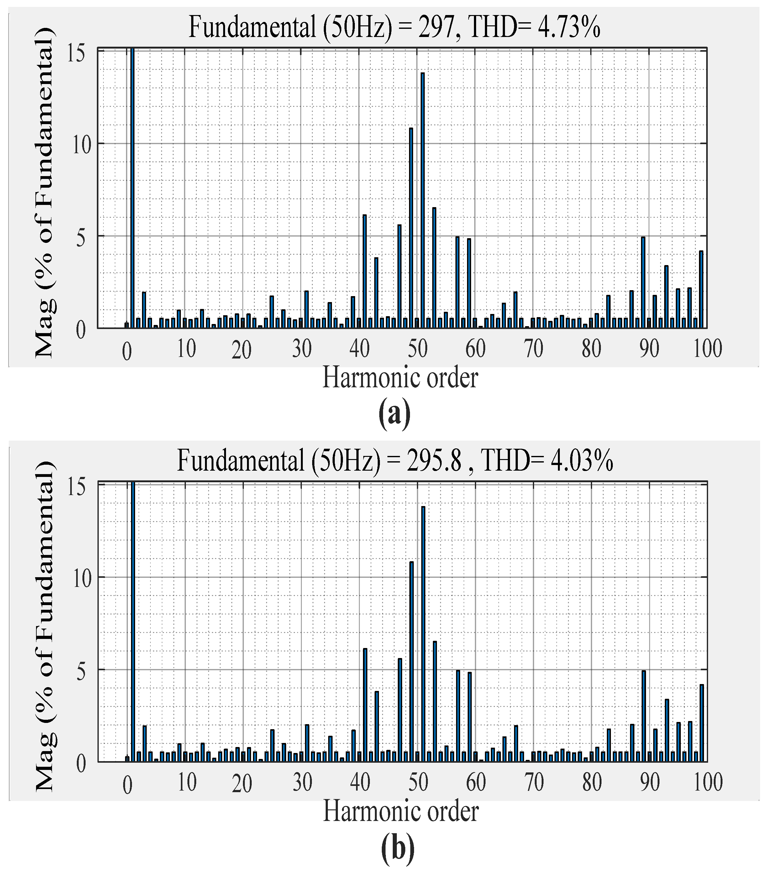
| Proposed | 17 | 1 | 13 | 3 | 3 | 8 | 53 | 6.623 | 2.06 | 2.42 | 4.03 |
Disclaimer/Publisher’s Note: The statements, opinions and data contained in all publications are solely those of the individual author(s) and contributor(s) and not of MDPI and/or the editor(s). MDPI and/or the editor(s) disclaim responsibility for any injury to people or property resulting from any ideas, methods, instructions or products referred to in the content. |
© 2024 by the authors. Licensee MDPI, Basel, Switzerland. This article is an open access article distributed under the terms and conditions of the Creative Commons Attribution (CC BY) license (https://creativecommons.org/licenses/by/4.0/).
Share and Cite
Choudhary, A.; Singh, A.K.; Mandal, R.K.; Saha, A.K. Switched Capacitor Inverter with Reduced Inrush Current and High Boosting Gain. Energies 2024, 17, 3064. https://doi.org/10.3390/en17133064
Choudhary A, Singh AK, Mandal RK, Saha AK. Switched Capacitor Inverter with Reduced Inrush Current and High Boosting Gain. Energies. 2024; 17(13):3064. https://doi.org/10.3390/en17133064
Chicago/Turabian StyleChoudhary, Ankita, Ashutosh Kumar Singh, Rajib Kumar Mandal, and Akshay Kumar Saha. 2024. "Switched Capacitor Inverter with Reduced Inrush Current and High Boosting Gain" Energies 17, no. 13: 3064. https://doi.org/10.3390/en17133064