Abstract
This paper proposes a single-phase, transformer-less, seven-level inverter that utilizes eight switches, three capacitors, and two diodes to produce seven voltage levels with triple boosting ability. The availability of the common-ground point eliminates the leakage current in PV applications. The proposed Transformer-Less Triple-Boosting Seven-Level Inverter (TLTB7LI) has the ability to feed different types of loads from non-unity to unity power factors. The voltage balancing of capacitors takes place naturally without the need for auxiliary circuits and complicated control strategies. This paper investigates the appropriateness of the proposed TLTB7LI for grid-connected application. The Peak Current Controller (PCC) is employed to generate the switching pulses and regulate the active/reactive power transfer between the converter and the output, which guarantees the high quality of injected current to the output. Moreover, the operational principles, its control technique, as well as the design procedure of the key components of the proposed inverter have been presented. The superiority of the proposed inverter over existing counterparts has been verified through comparative analysis. The simulation and experimental analysis validated the proper operation of the proposed TLTB7LI.
1. Introduction
In recent decades, the increasing demand for energy as well as the depletion of fossil fuels have urged human beings to switch toward renewable energies, like solar and wind, which are clean, renewable, vast, and free. The low DC output voltage of solar panels can be enhanced by step-up DC–DC converters and then converted to AC by inverters to feed the AC loads. The traditional two-level inverters usually require a large input DC voltage and bulky filters to reduce or cancel the low-order harmonics existing in the output voltage. The large voltage stress on switching devices, large switching losses, high common-mode voltage, and high total harmonic distortion of the output voltage are other demerits of the traditional two-level inverters. They also lack the voltage-boosting capability. On the other hand, the multilevel inverters (MLIs) as a new generation of power electronic converters are gaining remarkable popularity that originates from their inherent merits like having a simple structure, low harmonic content, high quality of output voltage, low voltage stress on the devices and load, and low electromagnetic interference (EMI) [1].
The classic MLIs are categorized into three families of Cascaded H-Bridge (CHB), Flying Capacitor (FC), and Neutral Point Clamped (NPC) inverters, which can suitably be applied in high power/voltage applications. Similar to traditional two-level inverters, they lack boosting capability. They also require a large number of devices to reach a higher number of levels. Furthermore, the latter two families require extra circuitry or control strategy to balance the charge of the capacitors [2].
The prior motivation in the development of new MLI structures is to reduce the number of required isolated DC sources as the most bulky, heavy, and costly parts [3]. This purpose can be satisfied by employing “DC–link” or “switched” capacitors. The former can provide the desired number of levels by reduced sources, but still misses the voltage-boosting ability. The switched-capacitor MLIs (SCMLIs) not only fulfill the “reduced-device” and “step-up capability” criteria but can also provide the natural voltage balancing of capacitors [4,5]. On the other hand, for high output power applications, large capacitances are required to suppress the voltage ripple of capacitors, which leads to bulky and costly structures. That is why the application of SCMLIs is usually limited to low/medium output powers, like residential applications.
In the literature, different SCMLI topologies have been presented for various on/off-grid applications. The availability of the Common Ground Point (CGP) as well as the voltage-boosting capability are essential features for PV–fed grid-tied inverters. The former feature tackles the leakage current of the PV panel, whereas the latter helps to further increase the low DC output voltage of the PV panel.
The authors of [6] present a triple-boosting seven-level SCMLI for renewable energy applications, which lacks the Common Ground Point (CGP) and requires a load-side H-bridge to form a bipolar output voltage waveform. Thus, four of the switches have to withstand the Maximum Output Voltage (MOV). Two modified versions have been presented in [7,8] that produce seven levels with a 1.5 boosting factor, where none of the switches withstand the MOV. The CGP feature has been missed. Two double-gain nine-level SCMLIs missing the CGP are presented in [9,10] that employ two half bridges to generate the negative levels. The two switches of [9] are exposed to the stress of the MOV, where none of the switches in [10] have to withstand the MOV. A common-grounded five-level SCMLI with a double boosting factor is presented in [11], where the switches suffer from large voltage stress. The two bidirectional switches (SB1, SB2) have to withstand the MOV. The voltage stress of the S2 and S3 switches is even greater than the MOV. A hybrid double-gain nine-level inverter including two switched-capacitor and flying-capacitor cells is presented in [12], which requires extra pre-charging circuitry for the charge balancing of the flying capacitor. Two quadruple-gain nine-level SCMLIs are presented in [13,14], which require an H-bridge to form the bipolar voltage waveform. Accordingly, the CGP feature is missed, and four switches have to tolerate the MOV.
As mentioned before, the SCMLIs are widely used in grid-connected PV applications [15]. A highly efficient common-grounded three-level SCMLI is presented in [16] for grid-tied PV applications that benefit from a low-size and eliminated leakage current but lack voltage-boosting ability. Another three-level inverter with more switches (compared to [16]) and similar features is presented in [17,18,19] that provides double voltage-boosting ability. The authors of [20] present a common-grounded double-gain five-level SCMLI, where the maximum voltage stress of the semiconductors is even greater than the MOV. Two common-grounded five-level SCMLIs are presented in [21,22] that their performance depends on the magnitude of the input source and can operate in dual modes of the buck or boost.. In the boost operational mode, the converters provide double voltage gain, while four switches have to withstand the MOV. Other similar common-grounded five-level SCMLI structures are presented in [23,24] that can operate only in step-up mode with a double voltage-boosting factor. In both converters, there are three switches withstanding the voltage of the MOV, but in [23] one of the switches (S6) has to tolerate twice the MOV, which is the main drawback of this converter. The converter presented in [24] can be extended to accomplish seven levels with a triple voltage-boosting factor. A reduced-component common-grounded five-level SCMLI is presented in [25] that lacks voltage-boosting ability. The authors of [26] present a seven-level SCMLI structure with an eliminated leakage current and a voltage-boosting factor of 1.5. The voltage stress of all semiconductors is within the input source voltage.
This paper proposes a common-grounded switched-capacitor seven-level inverter with eliminated leakage current that can be well-applied in grid-connected PV applications. The proposed topology provides a triple voltage-boosting factor, which is very beneficial in enhancing the low output voltage of PV to higher values. The proposed inverter benefits from the natural voltage balancing of the capacitors, which tackles the need for auxiliary circuitry or complicated control mechanisms. The proposed inverter can efficiently supply the pure–inductive or resistive–inductive load types with a variety of power factors, from zero to unity.
In the following sections, the configuration and operational principles of the proposed TLTB7LI are presented. Then, the employed PCC control scheme is elaborated upon. Section 4 provides a comparative analysis. In Section 5 and Section 6, the duty cycle calculation and design considerations of the proposed TLTB7LI are given. The experimental results are presented in Section 7. Finally, the conclusions are drawn in Section 8.
2. The Proposed Seven-Level Inverter
Figure 1a depicts the proposed single-phase transformer-less seven-level inverter that utilizes a single DC source, eight switches, three capacitors, and two diodes. Switches S2 and S3 are bidirectional blocking unidirectional conducting switches that can be realized by IGBTs without an anti-parallel diode or by reverse blocking IGBTs. The others are unidirectional blocking bidirectional conducting switches, which can be implemented by MOSFETs or IGBTs (with an anti-parallel diode). Table 1 presents the switching states of the proposed inverter and its capacitors’ charging/discharging status. In this table, the “green” arrow corresponds to the charge of the capacitors and the “red” arrow corresponds to the discharge state of the capacitors.
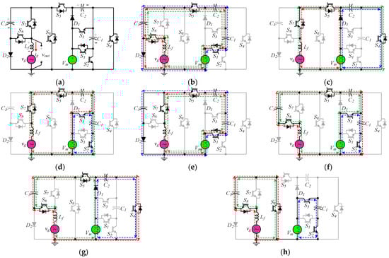
Figure 1.
(a) The proposed TLTB7LI configuration, the equivalent circuit of proposed seven-level inverter during the following states: (b) 1, (c) 2, (d) 3, (e) 4, (f) 5, (g) 6, (h) 7.

Table 1.
The switching scheme of the proposed inverter.
Figure 1b–h also show the equivalent circuit of the proposed inverter during different operational modes, where the “blue” line shows the capacitors’ charging path, the “red” line shows the active power flow path, and “green” line shows the reactive power flow path for grid/load current. Based on Figure 1b and Table 1, during the first state, the zero-voltage level is produced on the grid, where two different flow paths are available for the positive and/or negative grid current. In this state, the series connection of C1, C2, and the input source is paralleled with C3, which charges it to the sum of VC1, VC2, and Vin. Thus, C3 is charged to 3Vin. In the second state, Vout = Vin is generated, where C2 is paralleled with the input source and is charged to VC2 = Vin (Figure 1c). In the third state, C2 is cascaded with the source and Vout = 2Vin is produced on the load side. Meanwhile, C1 is paralleled with the source and is charged to VC1 = Vin (Figure 1d). In the fourth state, the input source, C1, and C2 are cascaded and produce Vout = 3Vin on the load, where C3 is paralleled with the series connection of Vin, C1, and C2 and is charged to VC3 = 3Vin (Figure 1e). Figure 1f presents the fifth state, where Vout = Vin + VC2 − VC3 = −Vin is generated. Simultaneously, C1 is connected in parallel with the source and is charged to VC1 = Vin. In the sixth state, Vout = Vin − VC3 = −2Vin is generated on the load port, where C2 is paralleled with the source and is charged to VC2 = Vin (Figure 1g). During the seventh state, C3 is paralleled with the load and produces Vout = −VC3 = −3Vin, where C1 is charged by the source to VC1 = Vin (Figure 1h). Thus, the voltage of the C1–C3 capacitors is naturally balanced, respectively, to Vin, Vin, and 3Vin. The peak output voltage of the proposed seven-level inverter is Vo,max = 3Vin, which leads to a triple boosting factor. Figure 1 confirms that the appropriate flow paths are available in the proposed seven-level inverter for positive and/or negative grid currents during all seven possible operational states, which confirms the reactive power transfer capability of the proposed inverter in grid connection applications. The voltage stresses (VS) of the semiconductors are as follows: S1: Vin, S2: Vin, S3: Vin, S4: 2Vin, S5: 2Vin, S6: 3Vin, S7: 3Vin, S8: 3Vin, D1: 2Vin, and D2: 3Vin. The Total Voltage Stress (TVS) is 21Vin. The per unit of TVS is equal to 7, as shown in (1).
3. PCC Control Scheme
In the literature, current controllers have become more widely used than other control methods in the transformer-less PV inverters. This is because current controllers have proven to be very quick and reliable, with almost no errors that persist over time in various situations within the grid. Meanwhile, the Peak Current Controller (PCC) method is a widely recognized type of traditional hysteresis current controller method. The general block diagram of the PCC control approach for the suggested inverter is shown in Figure 2. The suggested control system enables the injected current to accurately follow the desired reference current’s sinusoidal shape. Furthermore, as there are no conventional proportional–resonant or proportional–integrator controllers employed in this method, the injected current remains highly resilient under dynamic conditions. Figure 2 assumes that a PV panel with an MPPT block is present at the primary stage of the suggested inverter. The other main component of the system is the PCC unit, which serves as the controller block. It is possible to activate the power switch gates and control the active and reactive power injected into the grid. In general, the primary goal of this system is to inject a regulated current into the grid. To ensure the injected current has a rapid and reliable response, a phase-locked loop (PLL) system can be utilized as shown in Figure 2. This unit determines the suitable amplitude and phase for the grid.
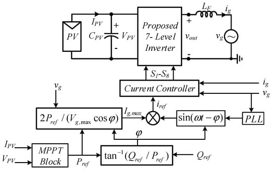
Figure 2.
The closed-loop control system of suggested inverter based on PCC method.
As depicted in Figure 2, the inverter’s filter (Lf) generates enough phase difference between vout and vg, whose difference enables power to be infused into the grid. Moreover, the maximum output power of a PV system is obtained by measuring the PV’s voltage and current and using a proper MPPT method. Afterward, the required phase and amplitude of the injected current (ig), which serves as the current reference (iref), is determined based on the desired active and reactive power values. In other words, the quantity of iref relies on Pref and Qref. Subsequently, iref is sent to the current controller block, and the PCC technique is implemented. Within the sampling time according to switching frequency (fsw), the measured current of the grid (ig) is compared with the reference current generated by the MPPT and PLL units. The switching patterns of the power switches involved are extracted by comparing iref with the measured value of ig as depicted in Figure 3 for the non-unity power factor (PF). From the PCC block, the slope and value of ig must be identified by examining the desired reference and measured currents during the sampling frequency so a comparison can be made. In order to produce seven different output voltage levels, it is necessary to define operating zones based on vg in relation to Vdc. This definition of operating zones serves as the second input data for the suggested PCC method. After analyzing ig and taking into account the specified operating zones, the switching pulses for the switches of the suggested inverter are derived. In the following, the functional principles of the suggested PCC technique in active power mode (PF = 1) and reactive power mode (PF ≠ 1) are explained. In Figure 3, the PCC technique produced seven levels of output voltage within six specified zones at PF ≠ 1. Figure 3 shows typical waveforms of ig, iref, vg, and vout, under the PF ≠ 1 mode. It is apparent that the system’s performance is determined by the instantaneous polarity of vg. In the PF ≠ 1 mode, the required angle and amplitude of iref should be identified first to create a proper reference waveform. The reference current has no influence on the six operating zones. It is necessary to identify in advance the particular zone that corresponds to the location of vg relative to the input voltage. However, in this mode, the direction of the injected current is from the grid to the inverter, so the polarity of Lf must be reversed. Once the measured value of ig at each operating zone exceeds iref, the upper output voltage level for each operating zone (vout,u) must be created to change the slope of the grid transition. Conversely, whenever ig is less than iref, a lower output voltage level for each operating zone (vout,l) must be generated. By making this switching transition, it is possible to fulfill the volt–second balanced principle of the inductor. At PF = 1, the injected current flows from the inverter to the grid; when the instant value of ig exceeds iref in each operating zone, the slope of ig will trend upwards. To maintain volt–second balance in Lf, the PCC generates a vout,l. Conversely, when the instant value of the injected current is less than the reference current, the slope will trend downwards, and vout,u is set. Figure 6 from reference [27] shows the implementation method of the PCC block.
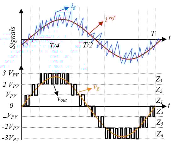
Figure 3.
Grid current and reference waveforms with division of zones.
4. Comparison
This section evaluates the superiority of the proposed seven-level inverter over its seven-level counterparts (presented in [28,29,30,31,32,33,34,35,36,37,38,39,40,41,42]) by performing a comprehensive analysis from the viewpoints of a number of devices, boosting factor (BF), natural voltage balancing of capacitors (NVB), per unit of the maximum voltage stress on the switching devices (MVSpu), per unit of the total voltage stress (TVSpu), inductive load feeding capability (ILF), availability of a Common Ground point (CG), H-Bridge requirement for negative level generation (HB), and Cost Function (CF). Table 2 presents the comparison results. In the implemented prototype of the proposed topology, the unidirectional conducting switches (S2–S3) have been realized by the series connection of a MOSFET and a diode, leading to two extra diodes, which have been considered in the comparisons. Moreover, to perform a fair comparison, only single-source (switched-capacitor, flying capacitor, or active neutral point clamped) seven-level topologies have been considered. The information presented in Table 2 has been shown as plots in Figure 4 to provide a better and clear view. According to Figure 4a, the topologies proposed in [28,31,34,35] lack the boosting ability, where the topologies in [28,31] operate as step-down inverters with the peak output voltage being less than the input voltage, and those in [34,35] provide a peak output voltage equal to the input voltage, leading to unity gain. The proposed topology and those in [29,30,32,33,36,37,38,39,40,41,42] are step-up inverters. The proposed topology and those in [30,33,37,40,42] provide triple boosting factor, which is the highest value among considered structures. Based on Figure 4b, the proposed inverter uses 8 IGBTs, as in [33,39], which is the minimum number among step-up converters. Also, according to Figure 4c, the proposed inverter requires only eight switches (and gate-drivers), which is the second least value among considered step-up inverters. From this point of view, [35] requires only six switches and gate-drivers among non-step-up topologies. As seen from Figure 4d, among boost inverters, [41] uses four capacitors to produce seven levels and a 1.5 boosting factor, while [30,33,37,42] require only two capacitors to provide the same levels and a triple boosting factor. On the contrary, the proposed seven-level triple-boosting topology requires three capacitors.
Table 2.
Comparison Results.
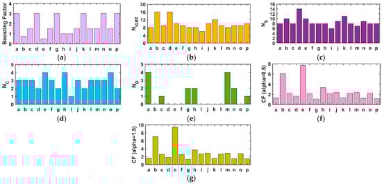
Figure 4.
Comparison results, a = Proposed, b = [28], c = [29], d = [30], e = [31], f = [32], g = [33], h = [34], i = [35], j = [36], k = [37], l = [38], m = [39], n = [40], o = [41], p = [42] (a) BF, (b) NIGBT, (c) NS, (d) NC, (e) ND, (f) CF (α = 0.5), (g) CF (α = 1.5).
Should the RB-IGBTs be applied toward realizing the unidirectional conducting switches (S2, S3), the proposed inverter will require only two diodes. However since the series connection of MOSFET and diode has been used for implementing the S2–S3 switches, the number of required diodes for the proposed inverter is four. Based on Figure 4e, among step-up topologies, [39] uses four diodes while [30,32,36,37,38,41] do not require any diode. The voltage balancing of the capacitors in the proposed and existing boost inverters [29,30,32,33,36,37,38,39,40,41,42] takes place naturally, but in non-boosting inverters [28,31,34,35], an extra control strategy or an auxiliary circuitry is required. The highest voltage stress (per unit) of semiconductors in [30] is only 0.33, which is mainly because of its numerous employed switching devices (Ns = 14, NIGBT = 16).
The peak per unit voltage stress on switching devices of [28,29,32,36,37,38,39,41] is about 0.67. The amount of this parameter for the proposed inverter is the same as that of [31,35,40,42] which is 1. The minimum TVS (per unit) among the considered boost inverters belongs to [29,32], which is 4.33. The TVS on semiconductors of the proposed inverter is 7, which is higher than others. As seen, the reduced-switch topologies (like the proposed topology) usually have large peak voltage stress and an accordingly large TVS on their semiconductors. All considered topologies, including the proposed inverter, are capable of feeding any load types (zero to unity power-factor loads). This property is essential, especially for grid-connected applications, where reactive power is required to be transferred. Among the considered topologies, the proposed inverter is the only one that benefits from a common-ground point, which accordingly eliminates the leakage current without any extra circuitry and/or complicated control strategy in PV applications. The topologies in [33,42] require an H-bridge at the load side to produce the negative voltage levels, where the H-bridge switches are exposed to peak output voltage stress. The proposed inverter and other structures do not require an H-bridge. To perform cost comparisons, the Cost Function (CF) used in [43] has been employed, as shown in (2). The CF analysis has been conducted for the TVS weighting coefficients of α = 0.5 and α = 1.5.
According to the comparative analysis, for α = 0.5 and α = 1.5, the proposed TLTB7LI has the fourth and fifth lowest CF among the considered 16 structures, respectively.
5. Duty Cycle Calculation for the Proposed Seven-Level Inverter
The output voltage of the inverter and the grid voltage are shown in Figure 5. It can be seen from Figure 6 that the output voltage of the inverter can be divided into six working zones. Working zones Z1 to Z3 correspond to the positive half cycle and working zones Z4 to Z6 correspond to the negative half cycle. The voltage and current of the grid in unity power factor can be expressed as follows:
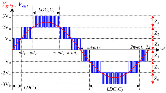
Figure 5.
Seven-level output voltage of the proposed inverter and grid voltage.
In working Zone 1, the grid voltage changes between 0 and +Vin. In order to calculate the duty cycle in this zone, the voltage balance equation for the output filter inductor Lf can be written as follows:
By simplifying (5), the duty cycle in Zone 1 is expressed as follows:
In relation to (5), Ts is the switching period of the inverter. In working Zone 2, the grid voltage changes between Vin and 2Vin, and in working Zone 3, the grid voltage changes between 2Vin and 3Vin. By writing the voltage balance law in the output filter inductor Lf and simplifying it, the duty cycle of the proposed inverter in Zones 2 and 3 is expressed as follows.
In relation to (8), T is the period time of the grid voltage. It is noted that the duty cycle in Zones 4, 5, and 6 is equal to Zones 1, 2, and 3, respectively, and their recalculation is omitted. Also, in order to calculate t1 and t2, the following equations can be used:
6. Design Procedure
In the proposed seven-level inverter, three capacitors and an output filter inductor are used. In this part, the value of the output filter inductor Lf, and the value of capacitors C1, C2, and C3 are calculated.
6.1. Calculation of the Output Filter Inductor
In order to calculate the value of the output filter inductor, the current equation can be written for the output filter inductor in each of the working zones. Since the maximum instantaneous output power of the inverter occurs at PF = 1 and for ωt = π/2, and ωt = π/2 is located in Zone 3, the current equation of the output filter inductor is written in this zone.
By simplifying (11) and inserting (8) into it, the inductor value of the output filter is obtained as follows:
At the unity power factor, the maximum current ripple of inductor Lf occurs at ωt = π/2. Therefore, the value of Lf for the maximum current ripple is calculated as follows:
6.2. Calculation of Capacitors C1, C2, and C3
In this part, the value of capacitors C1, C2, and C3 is calculated. In multi-level inverters, since the charging and discharging times of the capacitors are different, to calculate the capacitors, the maximum longest discharge (LDC) should be determined for each of the capacitors and the capacitance of the capacitors should be calculated from that. In Figure 5, the LDC is shown for each of the capacitors. By Relations (14)–(16), the value of the capacitors is calculated.
7. Experimental Verifications
In order to evaluate the performance of the proposed inverter and also confirm the theoretical analysis carried out in this paper, a number of experimental results are given in this section. These results are given in steady state and transient conditions so that the performance of the proposed inverter can be evaluated in different working conditions. Table 3 shows the active and passive elements as well as other specifications used in this section. The switches used in the experimental results section are G3R40MT12K and the diodes used are APT75DQ60BG. A TLP250 gate driver is also used to control switching on and off. A Texas Instrument microcontroller of the TMS320F28069 series has been used to control the proposed inverter and generate PWM pulses for the gate of the switches. A Chroma power supply of Model 62024P-600-8 is used to feed the input voltage of the proposed inverter, and its value is set at 133 V. Furthermore, the resistance value of the output load is 62 Ω. In Figure 6, the experimental setup of the proposed seven-level inverter is shown.
Table 3.
Parameter values of experimental analysis.
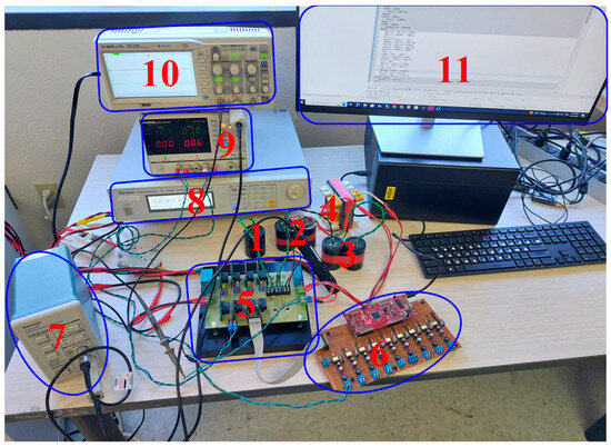
Figure 6.
Experimental setup of proposed seven-level inverter: (1) C1; (2) C2; (3) C3; (4) Lf; (5) power board, gate-driver cards, and heatsink; (6) TMS320F28069 microcontroller and interfacing board; (7) current prob; (8) chroma power supply; (9) power supply for gat-driver cards and interfacing board; (10) oscilloscope; (11) CCS12.3.0 software.
Due to the fact that the inverter is a switched-capacitor type, there is no need for an additional controller to balance the voltage of the capacitors and there is a natural voltage balance. Figure 7 shows the performance of the proposed inverter only in a steady state.
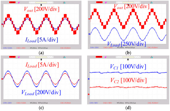
Figure 7.
Experimental results in 0.77kW output power: (a) seven-level inverter voltage and load current, (b) seven-level inverter voltage and load voltage, (c) load voltage and load current, and (d) voltage of capacitors C1 and C2.
In order to generate a sinusoidal voltage and current at both ends of the output load, an LC filter with an inductor value of 1.5 mH and a capacitor of 2.2 µF has been used. The switching frequency of the inverter is set to 20 kHz. Figure 7a shows the seven-level output voltage along with the load current. In fact, this figure shows the output voltage of the inverter before the filter, while the current shown is the current passing through the resistance of the output load. Figure 7b shows the inverter output voltage and the load voltage. According to this figure, the peak value of the seven-level output voltage is equal to 400 V, while the peak value of the load voltage is approximately 311 V, which corresponds to 220 Vrms. Figure 7c shows the load voltage and current for the proposed inverter. In this figure, the peak current of the load is 5 A and the peak voltage of the load is 311 V. Therefore, the output power is 0.77 kW. According to Figure 7a–c, the proposed inverter is able to produce a seven-level voltage at the output and a sinusoidal voltage at the load. Figure 7d shows that each of the capacitors of C1 and C2 are charged to the input voltage.
In order to show the performance of the inverter in transient mode and step change in the output power, Figure 8 is given. In Figure 8a,b, the inverter output voltage and load voltage along with load current are shown in step change mode in the load power. In these figures, the peak value of the load current has increased from 2.5 A to 5 A, which causes the power to increase from 0.38 kW to 0.77 kW. According to Figure 8a,b, in the condition of the step change in the value of output power, the load voltage and the output voltage of the inverter are stable. In order to show how the inverter turns on with the load, Figure 8c is given. Figure 8d also shows the output voltage and load current when the inverter is turned off. According to these figures, the proposed inverter does not have a transient mode when it is switched on and off. It is also important to note that in Figure 8c, the inverter capacitors are initially charged. In order to show the voltage of capacitors C1, C2, and C3 in step change conditions in the load, Figure 9a–c are shown. In this figure, the load power has been changed from 385 W to 770 W. In Figure 9a, the voltage of capacitor C1 is shown along with the load current. The peak current has increased from 2.5 A to 5 A, which increases the output power from 385 W to 770 W. According to this figure, the voltage of capacitor C1 at the moment before and after the step change of the load is still fixed at its nominal value and only the ripple of the capacitor voltage has increased after increasing the output power.
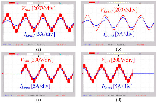
Figure 8.
Dynamic response: (a) inverter voltage with output load current in step change conditions in output power from 0.38 kw to 0.77 kW; (b) output load voltage with output load current in step change conditions in output power from 0.38 KW 0.77 KW; (c) seven-level inverter voltage with output load current in startup of the inverter; (d) seven-level inverter output voltage with output load current during inverter shutdown.
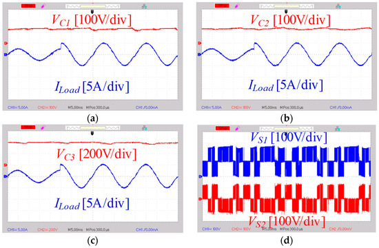
Figure 9.
Voltage of inverter capacitors with output load current in step change conditions in output power from 0.38 kW to 0.77 kW: (a) voltage of capacitor C1, (b) voltage of capacitor C2, (c) voltage of capacitor C3, and (d) voltage stress of S1 and S2 switches.
In Figure 9b,c, the voltage of capacitors C2 and C3 is shown along with the load current, respectively. It can be seen from these figures that the voltage of capacitors C2 and C3 at the moments before and after the step change still have a constant value and only their voltage ripple value has increased. Figure 9d shows the voltage stress of switches S1 and S2. According to this figure, the voltage stress of switch S1 is twice the input voltage. It can also be seen from Figure 9d that the voltage stress of switch S2 is equal to the input voltage and is also bidirectional. In other words, this switch blocks the voltage on both sides. In Figure 10a, the voltage of capacitor C3 is shown along with the voltage stress of diode D2. It can be seen that capacitor C3 is charged to three times the input voltage. Moreover, the voltage stress of diode D2 is triple that of the input voltage. Figure 10b shows the voltage stress of switches S3 and S4.
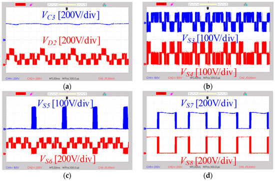
Figure 10.
(a) Voltage of capacitor C3 with voltage stress of diode D2, (b) voltage stress of switches S3 and S4, (c) voltage stress of switches S5 and S6, and (d) voltage stress of switches S7 and S8.
According to Figure 10b, the voltage stress of switch S3 is equal to the input voltage and the voltage stress of switch S4 is twice the input voltage. Furthermore, the voltage stress of switch S3 is bidirectional. Figure 10c is given to show the voltage stress of switches S5 and S6. According to this figure, the voltage stress of switch S5 is twice the input voltage and the voltage stress of switch S6 is three times the input voltage. Figure 10d is given to show the voltage stress of switches S7 and S8. The voltage stress of each of the switches, S7 and S8, is three times the input voltage. Finally, Figure 11a shows the performance of the proposed inverter at the moment of connecting the load to the output terminal. In this figure, the load enters the circuit at the instant ωt = 0. For this purpose, two MOSFET switches have been used back-to-back so that they can direct the current on both sides. According to this figure, the output voltage of the proposed inverter is stable at the moment of entering the load. Figure 11b shows the output load is disconnected from the circuit at the moment when ωt = 2π.
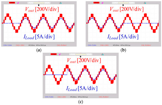
Figure 11.
Dynamic response and transient condition: (a) seven-level inverter voltage with output load current when connecting to inverter at ωt = 0, (b) seven-level inverter voltage with output load current when disconnecting from the inverter at ωt = π/2, (c) seven-level inverter voltage with output load current when connecting to inverter at ωt = π/2.
Finally, in Figure 11c, a very intense step change has occurred at the output terminal of the inverter. In this figure, the output load current has reached its maximum value of 5 A from zero. According to this figure, the output voltage of the inverter has a stable voltage in different conditions of step change and can feed the load connected to the output terminal. To evaluate the efficiency of the proposed inverter in different operating points, PSIM_2022.2 software has been used. In the simulation process, the parameters used in the simulation environment are the same as the ones used in the experimental setup. Figure 12 shows the efficiency diagram of the proposed converter for different output powers and different input voltages. In Figure 12a, the proposed converter works in the seven-level mode and the input voltage is 133 V. In this mode, the proposed inverter is in the boosting mode and the maximum efficiency occurred at the output power of 0.3 kW and is equal to 96.3%. In Figure 12b, the input voltage is equal to 200 V, and the proposed inverter works in the five-level mode. In this case, the converter is in the boosting mode. The maximum efficiency occurred at 0.2 kW and is equal to 98.5%. In Figure 12c, the efficiency of the converter is shown for the input voltage of 400 V. The converter works in the three-level mode and the maximum efficiency is equal to 99% and occurred at an output power of 0.8 kW. Finally, in Figure 12d, the loss breakdown related to the proposed converter is shown as a percentage. According to this figure, 46% of the total losses of the converter are related to the power switches, and the rest of the losses are related to other components.
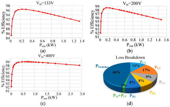
Figure 12.
Efficiencies of the proposed converter (a) with the input voltage of 133 V, (b) with the input voltage of 200 V, (c) with the input voltage of 400 V, (d) loss breakdown.
Figure 13 shows the injected current to the grid and its FFT analysis at an output power of 0.77 kW [44,45]. According to the IEEE-1547 standard [46], the injected current to the grid in grid-connected inverters should be less than 5%. As shown in Figure 13, the THD of the current is approximately 1.51%, which is lower than the IEEE-1547 standard limit. Additionally, Figure 14 shows the FFT analysis of the inverter’s output voltage before the output filter. According to this figure, the peak output voltage is 400 V and the main harmonic voltage is 311.2 V. The THD of the output voltage is 25.65%.
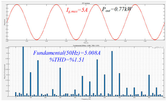
Figure 13.
FFT analysis of grid current at 0.77 kW output power.
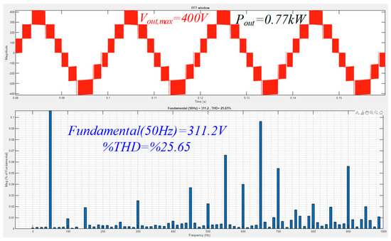
Figure 14.
FFT analysis of inverter output voltage before Lf filter.
8. Conclusions
A new power electronic converter is proposed in this paper based on SC technology. The proposed multi-level converter uses the advantage of common ground, which is very suitable for renewable energy systems, especially photovoltaics, and bypasses the scattering capacitors in PV systems. The proposed inverter has the capability of triple voltage boosting, which made it possible to inject power to the output load/grid at input voltages lower than the peak output voltage without the need of a boost converter. The operation modes of the proposed inverter were fully explained, and it was shown that the proposed inverter has the ability to handle reverse current, which is very important for non-unity power factor loads.
In short, the advantages of the proposed converter can be summarized as follows:
- -
- The common ground capability of the proposed inverter eliminates the leakage current in photovoltaic systems.
- -
- The ability to handle the return current by the proposed inverter makes it possible to feed non-unity power factor loads or perform voltage control at the point of common coupling of the power grid.
- -
- The ability to boost voltage with three times the gain means that there is no need for an additional boost converter, and at input voltages lower than the peak output voltage, power transfer is performed in a single-stage power processing.
- -
- The proposed inverter can inject power into the output power grid with a wide range of input voltage.
- -
- There is no need for an additional voltage sensor or a complex control system to control the voltage of the capacitors in the inverter.
- -
- It offers the high efficiency suitable for photovoltaic systems.
In order to show the advantages and disadvantages of the proposed inverter, a comprehensive comparison was made with other similar inverters, and the advantages and disadvantages of the proposed inverter were shown. The design of passive components in the proposed inverter was also provided in detail. Finally, several experimental results were given including steady state and transient conditions to show the superior performance of the proposed converter.
Author Contributions
Conceptualization, N.V.K.; methodology, K.V.; software, N.V.K.; validation, C.M., W.G. and Z.C.; formal analysis, N.V.K. and K.V.; investigation, J.F.A.; resources, W.G.; data curation, Z.C.; writing—original draft preparation, K.V., N.V.K. and J.F.A.; writing—review and editing, C.M.; visualization, N.V.K.; supervision, C.M.; project administration, C.M.; funding acquisition, C.M. All authors have read and agreed to the published version of the manuscript.
Funding
The authors would like to acknowledge the financial support of the California Energy Commission under grant number EPC-19-053.
Data Availability Statement
The data used in this study are publicly available and sources are referred.
Conflicts of Interest
The authors declare no conflicts of interest.
References
- Vijeh, M.; Rezanejad, M.; Samadaei, E.; Bertilsson, K. A general review of multilevel inverters based on main submodules: Structural point of view. IEEE Trans. Power Electron. 2019, 34, 9479–9502. [Google Scholar] [CrossRef]
- Trabelsi, M.; Vahedi, H.; Abu-Rub, H. Review on Single-DC-Source Multilevel Inverters: Topologies, Challenges, Industrial Applications, and Recommendations. IEEE Open J. Ind. Electron. Soc. 2021, 2, 112–127. [Google Scholar] [CrossRef]
- Salem, A.; Van Khang, H.; Robbersmyr, K.G.; Norambuena, M.; Rodriguez, J. Voltage source multilevel inverters with reduced device count: Topological review and novel comparative factors. IEEE Trans. Power Electron. 2020, 36, 2720–2747. [Google Scholar] [CrossRef]
- Barzegarkhoo, R.; Forouzesh, M.; Lee, S.S.; Blaabjerg, F.; Siwakoti, Y.P. Switched-capacitor multilevel inverters: A comprehensive review. IEEE Trans. Power Electron. 2022, 37, 11209–11243. [Google Scholar] [CrossRef]
- Kumari, M.; Siddique, M.D.; Sarwar, A.; Tariq, M.; Mekhilef, S.; Iqbal, A. Recent trends and review on switched-capacitor-based single-stage boost multilevel inverter. Int. Trans. Electr. Energy Syst. 2021, 31, e12730. [Google Scholar] [CrossRef]
- Khodaparast, A.; Hassani, M.J.; Azimi, E.; Adabi, M.E.; Adabi, J.; Pouresmaeil, E. Circuit configuration and modulation of a seven-level switched-capacitor inverter. IEEE Trans. Power Electron. 2020, 36, 7087–7096. [Google Scholar] [CrossRef]
- Zhao, J.; Chen, Y.; Zeng, J.; Liu, J. Low-voltage stress seven-level inverter based on symmetrical capacitors. IEEE J. Emerg. Sel. Top. Power Electron. 2021, 10, 3033–3044. [Google Scholar] [CrossRef]
- Wang, Y.; Yuan, Y.; Li, G.; Ye, Y.; Wang, K.; Liang, J. A T-type switched-capacitor multilevel inverter with low voltage stress and self-balancing. IEEE Trans. Circuits Syst. I Regul. Pap. 2021, 68, 2257–2270. [Google Scholar] [CrossRef]
- Naik, B.S.; Suresh, Y.; Venkataramanaiah, J.; Panda, A.K. A hybrid nine-level inverter topology with boosting capability and reduced component count. IEEE Trans. Circuits Syst. II Express Briefs 2020, 68, 316–320. [Google Scholar] [CrossRef]
- Siddique, M.D.; Karim, M.F.; Mekhilef, S.; Rawa, M.; Seyedmahmoudian, M.; Horan, B.; Stojcevski, A.; Ahmed, M. Single-phase boost switched-capacitor-based multilevel inverter topology with reduced switching devices. IEEE J. Emerg. Sel. Top. Power Electron. 2021, 10, 4336–4346. [Google Scholar] [CrossRef]
- Kumari, S.; Verma, A.; Sandeep, N.; Yaragatti, U.R.; Pota, H. A five-level transformer-less inverter with self-voltage balancing and boosting ability. IEEE Trans. Ind. Appl. 2021, 57, 6237–6245. [Google Scholar] [CrossRef]
- Zhao, J.; Chen, Y.; Zeng, J.; Liu, J. A hybrid nine-level inverter with reduced components and simplified control. IEEE J. Emerg. Sel. Top. Power Electron. 2022, 10, 4498–4508. [Google Scholar] [CrossRef]
- Sathik, M.A.; Siddique, M.D.; Sandeep, N.; Hota, A.; Almakhles, D.; Mekhilef, S.; Yaragatti, U.R. Compact Quadratic Boost Switched-Capacitor Inverter. IEEE Trans. Ind. Appl. 2022, 58, 4923–4931. [Google Scholar] [CrossRef]
- Varesi, K.; Esmaeili, F.; Deliri, S.; Tarzamni, H. Single-Input Quadruple-Boosting Switched-Capacitor Nine-Level Inverter with Self-Balanced Capacitors. IEEE Access 2022, 10, 70350–70361. [Google Scholar] [CrossRef]
- Khan, N.H.; Forouzesh, M.; Siwakoti, Y.P.; Li, L.; Kerekes, T.; Blaabjerg, F. Transformerless inverter topologies for single-phase photovoltaic systems: A comparative review. IEEE J. Emerg. Sel. Top. Power Electron. 2020, 8, 805–835. [Google Scholar] [CrossRef]
- Ardashir, J.F.; Sabahi, M.; Hosseini, S.H.; Blaabjerg, F.; Babaei, E.; Gharehpetian, G.B. A single-phase transformerless inverter with charge pump circuit concept for grid-tied pv applications. IEEE Trans. Ind. Electron. 2016, 64, 5403–5415. [Google Scholar] [CrossRef]
- Vosoughi, N.; Hosseini, S.H.; Sabahi, M. Single-phase common-grounded transformer-less grid-tied inverter for PV application. IET Power Electron. 2020, 13, 157–167. [Google Scholar] [CrossRef]
- Vosoughi, N.; Hosseini, S.H.; Sabahi, M. A new single-phase transformerless grid-connected inverter with boosting ability and common ground feature. IEEE Trans. Ind. Electron. 2019, 67, 9313–9325. [Google Scholar] [CrossRef]
- Kurdkandi, N.V.; Marangalu, M.G.; Vala, S.S.; Mohseni, P.; Gharehkoushan, A.R.Z.; Hosseini, S.H.; Sabahi, M. A new transformer-less common grounded three-level grid-tied inverter with voltage boosting capability. IEEE Trans. Energy Convers. 2020, 36, 1896–1909. [Google Scholar] [CrossRef]
- Vosoughi, N.; Hosseini, S.H.; Sabahi, M. A new transformer-less five-level grid-tied inverter for photovoltaic applications. IEEE Trans. Energy Convers. 2020, 35, 106–118. [Google Scholar] [CrossRef]
- Khan, M.N.; Siwakoti, Y.P.; Scott, M.J.; Li, L.; Khan, S.A.; Lu, D.D.; Barzegarkhoo, R.; Sidorski, F.; Blaabjerg, F.; Hasan, S.U. A common grounded type dual-mode five-level transformerless inverter for photovoltaic applications. IEEE Trans. Ind. Electron. 2020, 68, 9742–9754. [Google Scholar] [CrossRef]
- Barzegarkhoo, R.; Siwakoti, Y.P.; Aguilera, R.P.; Khan, N.H.; Lee, S.S.; Blaabjerg, F. A novel dual-mode switched-capacitor five-level inverter with common-ground transformerless concept. IEEE Trans. Power Electron. 2021, 36, 13740–13753. [Google Scholar] [CrossRef]
- Barzegarkhoo, R.; Siwakoti, Y.P.; Blaabjerg, F. A new switched-capacitor five-level inverter suitable for transformerless grid-connected applications. IEEE Trans. Power Electron. 2020, 35, 8140–8153. [Google Scholar] [CrossRef]
- Barzegarkhoo, R.; Lee, S.S.; Khan, S.A.; Siwakoti, Y.; Lu, D.D.-C. A novel generalized common-ground switched-capacitor multilevel inverter suitable for transformerless grid-connected applications. IEEE Trans. Power Electron. 2021, 36, 10293–10306. [Google Scholar] [CrossRef]
- Guo, B.; Zhang, X.; Su, M.; Ma, H.; Yang, Y.; Siwakoti, Y.P. A single-phase common-ground five-level transformerless inverter with low component count for PV applications. IEEE Trans. Ind. Electron. 2023, 70, 2662–2674. [Google Scholar] [CrossRef]
- Gao, Y.; Zhang, W.; Zarnaghi, Y.N.; Kurdkandi, N.V.; Zhang, C. A new boost switched capacitor seven-level grid-tied inverter. IET Power Electron. 2021, 14, 268–279. [Google Scholar] [CrossRef]
- Kurdkandi, N.V.; Marangalu, M.G.; Mohammadsalehian, S.; Tarzamni, H.; Siwakoti, Y.P.; Islam, R.; Muttaqi, K.M. A New Six-Level Transformer-Less Grid-Connected Solar Photovoltaic Inverter with Less Leakage Current. IEEE Access 2022, 10, 63736–63753. [Google Scholar] [CrossRef]
- Pulikanti, S.R.; Konstantinou, G.; Agelidis, V.G. Hybrid seven-level cascaded active neutral-point-clamped-based multilevel converter under SHE-PWM. IEEE Trans. Ind. Electron. 2012, 60, 4794–4804. [Google Scholar] [CrossRef]
- Liu, J.; Wu, J.; Zeng, J. Symmetric/Asymmetric hybrid multilevel inverters integrating switched-capacitor techniques. IEEE J. Emerg. Sel. Top. Power Electron. 2018, 6, 1616–1626. [Google Scholar] [CrossRef]
- Lee, S.S. A single-phase single-source 7-level inverter with triple voltage boosting gain. IEEE Access 2018, 6, 30005–30011. [Google Scholar] [CrossRef]
- Anderson, J.A.; Hanak, E.J.; Schrittwieser, L.; Guacci, M.; Kolar, J.W.; Deboy, G. All-Silicon 99.35% efficient three-phase seven-level hybrid neutral point clamped/flying capacitor inverter. CPSS Trans. Power Electron. Appl. 2019, 4, 50–61. [Google Scholar] [CrossRef]
- Zeng, J.; Lin, W.; Liu, J. Switched-capacitor-based active-neutral-point-clamped seven-level inverter with natural balance and boost ability. IEEE Access 2019, 7, 126889–126896. [Google Scholar] [CrossRef]
- Peng, W.; Ni, Q.; Qiu, X.; Ye, Y. Seven-level inverter with self-balanced switched-capacitor and its cascaded extension. IEEE Trans. Power Electron. 2019, 34, 11889–11896. [Google Scholar] [CrossRef]
- Siwakoti, Y.P.; Mahajan, A.; Rogers, D.J.; Blaabjerg, F. A novel seven-level active neutral-point-clamped converter with reduced active switching devices and DC-link voltage. IEEE Trans. Power Electron. 2019, 34, 10492–10508. [Google Scholar] [CrossRef]
- Vahedi, H.; Al-Haddad, K. Real-time implementation of a seven-level packed U-cell inverter with a low-switching-frequency voltage regulator. IEEE Trans. Power Electron. 2015, 31, 5967–5973. [Google Scholar] [CrossRef]
- Sathik, M.J.; Sandeep, N.; Blaabjerg, F. High gain active neutral point clamped seven-level self-voltage balancing inverter. IEEE Trans. Circuits Syst. II Express Briefs 2019, 67, 2567–2571. [Google Scholar] [CrossRef]
- Siddique, M.D.; Mekhilef, S.; Shah, N.M.; Ali, J.S.M.; Blaabjerg, F. A new switched capacitor 7L inverter with triple voltage gain and low voltage stress. IEEE Trans. Circuits Syst. II Express Briefs 2019, 67, 1294–1298. [Google Scholar] [CrossRef]
- Lee, S.S.; Lim, C.S.; Siwakoti, Y.P.; Lee, K.-B. Hybrid 7-level boost active-neutral-point- clamped (H-7L-BANPC) inverter. IEEE Trans. Circuits Syst. II Express Briefs 2019, 67, 2044–2048. [Google Scholar] [CrossRef]
- Sivasubramanian, M.; Boopathi, C.S. A switched capacitor based seven level active neutral point clamped (anpc) inverter topology with reduced switching devices. J. Electr. Eng. Technol. 2021, 16, 3103–3112. [Google Scholar] [CrossRef]
- Roy, T.; Tesfay, M.W.; Nayak, B.; Panigrahi, C.K. A 7-level switched capacitor multilevel inverter with reduced switches and voltage stresses. IEEE Trans. Circuits Syst. II Express Briefs 2021, 68, 3587–3591. [Google Scholar] [CrossRef]
- Agarwal, R.; Gupta, K.K.; Singh, S. Switched capacitors-based single-phase seven-level photovoltaic inverter with self-voltage balancing. Electr. Eng. 2022, 104, 3107–3117. [Google Scholar] [CrossRef]
- Kishore, P.S.V.; Jayaram, N.; Jakkula, S.; Sankar, Y.R.; Rajesh, J.; Halder, S. A new reduced switch seven-level triple boost switched capacitor based inverter. IEEE Access 2022, 10, 73931–73944. [Google Scholar] [CrossRef]
- Roy, T.; Sadhu, P.K. A Step-Up Multilevel Inverter Topology Using Novel Switched Capacitor Converters with Reduced Components. IEEE Trans. Ind. Electron. 2020, 68, 236–247. [Google Scholar] [CrossRef]
- Liao, K.; Pang, B.; Yang, J.; He, Z. Output Current Quality Improvement for VSC with Capability of Compensating Voltage Harmonics. IEEE Trans. Ind. Electron. 2023, 71, 9087–9097. [Google Scholar] [CrossRef]
- Pang, B.; Zhu, X.; Yang, J.; Liao, K.; Chen, B.; He, Z. Voltage Harmonics Optimization for Weak Grid-Tied Doubly-Fed Induction Generator with the Capability of Suppressing Current Harmonics. IEEE Trans. Energy Convers. 2023, 38, 1452–1460. [Google Scholar] [CrossRef]
- IEEE Std 1547-2018 (Revision of IEEE Std 1547-2003); IEEE Standard for Interconnection and Interoperability of Distributed Energy Resources with Associated Electric Power Systems Interfaces. IEEE: New York, NY, USA, 2018.
Disclaimer/Publisher’s Note: The statements, opinions and data contained in all publications are solely those of the individual author(s) and contributor(s) and not of MDPI and/or the editor(s). MDPI and/or the editor(s) disclaim responsibility for any injury to people or property resulting from any ideas, methods, instructions or products referred to in the content. |
© 2024 by the authors. Licensee MDPI, Basel, Switzerland. This article is an open access article distributed under the terms and conditions of the Creative Commons Attribution (CC BY) license (https://creativecommons.org/licenses/by/4.0/).