1. Introduction
Capacitors in power systems serve multiple functions including filtering, compensating for reactive power losses, reducing line losses, improving system power factor, and lowering investment and operational costs making them widely applicable [
1,
2,
3,
4]. However, due to the harmonics present in power systems and the varying external environmental temperatures, capacitors frequently encounter various types of faults, such as thermal breakdown, electrical breakdown, fuse failure and bushing faults [
5,
6,
7,
8], which are greatly influenced by the internal electric field distribution within the capacitor [
9,
10,
11]. In consequence, it is urgently necessary to verify the accuracy of the insulation structure design, specifically the validity of the electric field simulation results, to achieve precise design and verification of the insulation structure.
As research on capacitor electric field distribution by scholars has deepened, it has become evident that the internal insulation structure of capacitors—such as film thickness, compression coefficient, the distance between the capacitor and the casing, and the winding process—significantly affects their performance. T. Umemura and K. Abe [
12,
13] discovered that using a folded-edge structure in all-film power capacitors can improve the edge electric field. They calculated the field stress along the direction of maximum field stress and experimentally validated that the partial discharge inception voltage of capacitors with folded-edge structures is lower. Chenmeng Zhang [
14,
15] et al. simulated defects that might be distributed in the arc region of impact capacitors and conducted a simulation analysis of their electric field, concluding that the maximum field stress is lower when the defect area is impregnated compared to when it is filled with air. Bing Wang [
16] analyzed the end electric field of all-film capacitors under different impregnation conditions and compression coefficients, finding that increasing the compression coefficient can significantly improve the end electric field distribution in impregnated capacitors. In non-impregnated conditions, the electric field distortion coefficient increases with the compression coefficient; in impregnated conditions, the coefficient decreases with increasing compression. Zhongyuan Mei [
17] performed finite element simulations on the edge electric field of different high-voltage power capacitor designs, altering parameters such as plate thickness, polypropylene film thickness between plates, and edge characteristic thickness. They found that the maximum field stress in all-film capacitors can be obtained by multiplying the average field stress by the electric field distortion coefficient. Increasing the total dielectric thickness between plates increases the electric field distortion coefficient and edge field stress.
Given that actual capacitors are immersed in insulating liquid, measuring the electric field between the capacitor element and the casing poses significant challenges. Current simulations of capacitor electric fields rely heavily on models that lack empirical data, particularly regarding the influence of internal insulation structures on the electric field, which hinders the ability to objectively reflect the actual electric field distribution characteristics within capacitors.
To address the aforementioned issues, this study utilizes the Kerr electro-optic effect to focus on electric field-concentrated positions, such as the ends of capacitor elements. We have established a non-contact optical remote sensing system to measure the spatial electric field distribution between the capacitor element and the case. By selecting capacitor element models with different main insulation distances and other structural characteristics, this study conducts empirical research on the spatial electric field distribution in the oil between the capacitor element and the case in oil-immersed capacitors.
2. Experimental Platform
2.1. Electric Field Measuring Platform
2.1.1. Kerr Electro-Optic Effect
In 1990, the application of the Kerr electro-optic effect method using AC modulation gradually gained prominence [
18,
19,
20]. Currently, measuring the electric field in liquid using the birefringent Kerr effect has been proven to be an effective and reliable method. The Kerr effect method has several distinct advantages: it can reflect real-time changes in the electric field without affecting the measured field, and it offers higher accuracy. Various research institutions have further developed and refined this method. For example, the authors’ research team have established a non-contact, temperature-controlled platform for measuring electric fields in oil to study the electric fields in insulating media [
21,
22,
23,
24], which can provide a reference for setting up a platform to measure the electric field in oil-immersed capacitors in this study.
The principle of Kerr electro-optic effect measurement is that under an externally applied electric field, isotropic transparent dielectric materials exhibit optical anisotropy, causing refraction. Light perpendicular to the electric field direction and light parallel to the electric field direction will develop a phase difference due to the electric field and this difference is related to the electric field stress. This relationship can be expressed as shown in Equation (1):
where
B is the Kerr constant of the liquid in m/V
2,
L is the length of the uniform electric field region to be measured in m,
E is the AC electric field stress in V/m.
(1) Linearly polarized light generation element: A helium-neon laser. A 632.8 nm helium-neon laser beam with excellent spot characteristics and stability was selected based on measurement requirements.
(2) Polarizing element to convert random light into polarized light: Polarizer and analyzer. The most important parameter is the extinction ratio, for which a Glan–Taylor polarizer with an extinction ratio greater than 105 was chosen to meet experimental requirements.
(3) Element to convert linearly polarized light into circularly polarized light: Quarter-wave plate. The critical parameter here is phase retardation accuracy. A quartz zero-order wave plate with a retardation accuracy of λ/300 was selected to ensure precision.
(4) Light intensity processing element: Photodetector.
(5) Electrical signal processing element: Lock-in amplifier. To output the corresponding fundamental and harmonic components, a SynkTek MCL1-40 lock-in amplifier from SynkTek AB, Switzerland, was utilized.
The entire system is shown in
Figure 1, and it employs a single optical path structure. The helium-neon laser emitter generates linearly polarized light, which, after passing through a polarizer and a quarter-wave plate, transforms into circularly polarized light. This circularly polarized light is then directed into the capacitor element-casing electric field measurement cavity. Within the cavity, the circularly polarized light, carrying electric field and phase information, becomes elliptically polarized light. Finally, this elliptically polarized light passes through an analyzer, creating polarized light interference.
Since the direction of the AC electric field is known, it is necessary to set the transmission directions of the polarizer and analyzer to be orthogonal to each other. Let the analysis angle be 3π/4, and the angle between the optical axis direction of the quarter-wave plate and the transmission direction of the polarizer be π/4. The formula for calculating the capacitor element-casing electric field is then given as Equation (2).
where
Idc denotes the DC light intensity component in V,
I2ω denotes the frequency-doubled component in μV. By simultaneously measuring a set of DC light intensity components
Idc and harmonic components
I2ω using a photodetector and a lock-in amplifier, the externally applied AC electric field stress can be determined using Equation (2).
2.1.2. Power Supply Unit
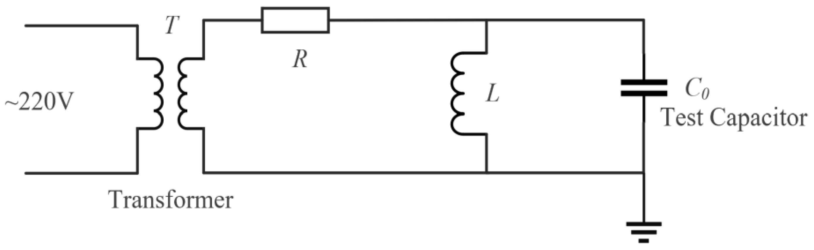
Since the impedance of the capacitor is less than 500 Ω, an applied test voltage of 3.3 kV results in a current exceeding 7 A; consequently, general power supplies are inadequate for such high current requirements. Therefore, a test plan has been designed wherein a high-power transformer, with a capacity of 40 kVA, is connected to the capacitor, as depicted in
Figure 2. This arrangement supports the application of a 7 A current on the high-voltage side, thereby ensuring that both the voltage and current on the capacitor meet the specified test requirements.
2.1.3. Experimental Cavity
Capacitors need to withstand complex temperature environments under actual working conditions, and the test can accommodate electric field measurements at temperatures ranging from 20 °C to 80 °C. The temperature measurement module is primarily composed of three materials: a stainless steel cavity, a silicone heating sheet, and a rubber insulation layer. It is equipped with a temperature controller, which allows for rapid heating within 30 min.
The capacitor casing and the inner cavity of the capacitor cavity are made of stainless steel. A polytetrafluoroethylene (PTFE) sheath is placed on the outside of the symmetrical brass guide rod. A dynamic seal is located at the connection with the guide rod to ensure air tightness. Additionally, a groove-filled sealing ring is positioned at the connection with the cavity for sealing purposes. Quartz glass is used for the laser entrance and exit window. The schematic diagram and actual picture of the test cavity are shown in
Figure 3.
The key components of the cavity include:
(1) Stainless Steel Cavity: The inner cavity and outer casing of the capacitor’s electric field measurement cavity are made of stainless steel.
(2) Stainless Steel Casing: Simulates the casing of the capacitor under actual operating conditions.
(3) Brass Guide Rods: Composed of two rods, with one connected to high voltage and the other grounded during the experiment.
(4) Polypropylene Sheath: PTFE sheaths are placed on the outside of the brass guide rods to ensure the rods do not directly contact the casing.
(5) Gaskets: Serve to insulate and elevate the capacitor.
(6) Quartz Glass: Since the experiment requires testing the electric field at different temperatures, quartz glass was chosen for its high transmittance (>99%) and minimal deformation across varying temperatures, using anti-reflective coated quartz windows.
The rated voltage of the applied high-voltage all-film capacitors is 3.3 kV. Therefore, an electric field simulation with an external voltage of 3.3 kV was conducted on the capacitor element-casing electric field distribution measurement cavity. The resulting electric field distribution within the cavity is illustrated in
Figure 4. The maximum field stress in the PTFE sheath is located at the bottom of the sheath near the screw, reaching 1.404 kV/mm. Meanwhile, the maximum field stress in the cavity is at the contact point between the sheath and the cavity casing, with a peak field stress of 4.90 kV/mm. In the electric field simulation of the cavity external voltage, it can be seen that the highest electric field stress is located at the bottom of the sheath near the screws. The maximum that field stress of the PTFE sheath used in the cavity can withstand is higher than 20 kV/mm. When the external voltage is 10 kV, the maximum field stress of the cavity sheath is 15.2 kV/mm, taking into account 20% of the insulation margin, which can satisfy the insulation stress of the PTFE sheath. Considering a 20% insulation margin, the insulation stress of the PTFE sheath can be satisfied, so the cavity can theoretically withstand the maximum voltage of 10 kV.
To ensure the accuracy of the experimental data, the sensitivity of the electric field measurement system needs to be calibrated before the experiment. The sensitivity calibration experiment uses a 10 mm flat element calibration method. By comparing the actual measured value with the theoretical value, the sensitivity of the measurement system is determined. The frequency of the external AC voltage is 50 Hz, and the external voltage is gradually varied to 500 V, 1000 V, 2000 V, and 3000 V, which corresponds to electric field stress of 0.05 kV/mm, 0.10 kV/mm, 0.20 kV/mm, 0.30 kV/mm, respectively. After fitting, the linearity reaches 0.9997, indicating that the system has high accuracy and is suitable for conducting measurements, and the fitting results are shown in
Figure 5.
2.2. Electric Field Measuring Area and Measuring Points
This test primarily investigates the electric field distribution between the capacitor element and the casing. Therefore, the measurement area is selected as the external liquid domain between the capacitor element and the casing, as shown in
Figure 6. Eleven measurement paths were taken within the liquid domain to measure the electric field stress. Since the capacitor model is completely symmetrical in the simulation, only eight points in the upper half need to be considered.
The dimensions of the capacitor casing are 388 × 179 × 480 mm. If the fixed capacitor is located at the center of the casing, the edge of the capacitor is 5.5 mm from the vertical edge of the casing and 25 mm from the upper edge. Therefore, eight symmetrical measurement points are set up and down, as illustrated in
Figure 7. In
Figure 7, five electric field measurement points are set in the X direction, with a spacing of 1 mm, labeled as 1, 2, 3, 4, and 5. Additionally, nine electric field measurement points are set on both Y1 and Y2 directions, with a spacing of 1 mm. The central point is labeled as point 1, and the points along the positive directions of Y1 and Y2 are labeled as points 2, 3, 4, and 5, respectively.
It is now generally accepted that the edge region of the capacitor element is a point of electric field concentration with weak insulation [
25]. Therefore, the maximum field stress of an oil-immersed capacitor occurs at the edge of the plate. For the spatial electric field in the element-casing liquid, there is a slightly uneven electric field near the end of the element, with an electric field unevenness coefficient not exceeding 1.1. The simulation results of the electric field unevenness at each measurement point are shown in
Table 1. When the electric field unevenness does not exceed 1.1, the Kerr effect phase difference can be controlled within 1.5% and the electric field measurement error can be controlled at around 1.3% [
26,
27].
2.3. Calibration of Kerr’s Constant
When conducting Kerr constant measurements, flat plate electrodes are used with a fixed spacing of 10 mm. The upper electrode is subjected to an alternating current voltage, ranging from 0.5 kV to 3 kV, while the lower electrode is grounded. Under these conditions, the electric field stress within the liquid medium is a known quantity. Therefore, based on the principle of the Kerr electro-optic effect, the Kerr constant of benzyltoluene can be deduced by utilizing the electrode length, known electric field stress, and the measured direct current component (
Idc) and double-frequency component (
I2ω), in conjunction with the following Equation (2). Additionally, by applying different temperatures to the test chamber, specifically at 20 °C, 40 °C, 60 °C, and 80 °C, the Kerr constant of the liquid medium at various temperatures can be determined, as detailed in
Table 2.
3. Spatial Electric Field Distribution Characteristics
3.1. Simulation Model
The capacitor core comprises multiple stacked capacitor elements, each wound from two layers of aluminum foil and three layers of film. This study investigates a single capacitor element, where the multilayer winding structure is converted into a single-layer configuration. The capacitor simulation model, depicted in
Figure 8, primarily includes benzyltoluene, polypropylene film, inner electrodes, outer electrodes, and a casing.
The materials and parameters for each part are shown in
Table 3. In the simulation model, the inner and outer electrodes are made of aluminum, the casing material is stainless steel, and the film and impregnating agent are polypropylene and benzyltoluene, respectively. Their conductivities and relative permittivity are provided by measured parameters.
3.2. The Variation of Electric Field Distribution with Different Sampling Directions
Taking the electric field stress measurements at 20 °C for measurement points 1, 3, and 5 in the X direction as an example, the variation of spatial electric field stress at different positions over time is shown in
Figure 9. During the tests, due to the brief pressurization process (10–15 s), changes in the electric field during this period are omitted from the data recording in this study. Once the externally applied voltage reaches the preset value and stabilizes, the recording of the electric field dynamics begins. As the applied voltage is alternating current, the electric field distribution strictly adheres to the RC (resistance–capacitance) model, rapidly achieving a steady state. Only interfacial polarization charges are present, with no generation of other forms of charges, such as ionization or injected charges, resulting in no significant changes in electric field stress as the voltage application time extends. Therefore, in the subsequent analysis, this paper uses the average spatial electric field stress over a 900 s measurement period as the analysis subject.
The internal structure of the 12 μm capacitor consists of 12 + 13 + 12 μm film wound together. As shown in
Figure 7, the measurement points are divided into two groups: five points in the X direction and four points each in the Y1 and Y2 directions. The comparisons result for the electric field in the X and Y directions are shown in
Figure 10.
In both the X and Y directions, the electric field distribution exhibits a negative decay trend as the distance from the sampling points to the capacitor element increases. In the Y direction, the measured values at the upper Y1 points are basically consistent to those at the lower Y2 points.
Comparing the simulated and measured data for the element-casing electric field of the capacitor, the measured electric field values are higher than the simulated values in both the X and Y directions. The measured value at point 5 in the X direction is 19% higher than the simulated value, while the measured value at point 3 in the Y direction is 23% higher than the simulated value. On average, the measured values are 15% higher than the simulated values. Additionally, as the distance between the measurement point and the capacitor element increases, the closer the measurement point is to the casing, and the smaller the difference between the simulated and measured values becomes.
3.3. The Variation of Electric Field Distribution with Different Distances of Main Insulation
During transportation and installation, capacitor elements may not remain centered within the casing, which can alter the main insulation distance between the edges of the capacitor elements and the casing. To simulate these variations, both experimental and simulation setups were designed to account for five different main insulation distances: 5.5 mm, 4.5 mm, 3.5 mm, 2.5 mm, and 1.5 mm. This approach allowed for a detailed analysis of how the element-casing electric field stress changes when the capacitor elements shift, and the characteristics of the capacitor field stresses at different main insulation distances are shown in
Figure 11.
As the main insulation distance varies, the electric field stress at each measurement point continues to exhibit a negative correlation with increasing insulation distance. The reduction in electric field stress is more pronounced at shorter insulation distances. At these shorter distances, the field stress decreases rapidly with increasing measurement distance. Conversely, as the measurement distance increases, the impact of the main insulation distance on the field stress at each point diminishes gradually. For instance, at measurement point 1, the field stress at a main insulation distance of 4.5 mm is 1.1 times that at 5.5 mm. When the distance is reduced to 3.5 mm, the field stress becomes 1.14 times that at 5.5 mm. Further reduction to 2.5 mm results in a field stress 1.31 times that at 5.5 mm, and at 1.5 mm, it reaches 1.81 times that at 5.5 mm.
Figure 12 compares the simulated and measured values of the element-casing electric field at main insulation distances of 5.5 mm and 3.5 mm. It is observed that the measured electric field values are consistently higher than the simulated ones. Moreover, the discrepancy between the simulated and measured values increases as the main insulation distance decreases. Specifically, at a main insulation distance of 5.5 mm, the measured electric field value is 15% higher than the simulated value. This discrepancy grows to 17% when the main insulation distance is reduced to 3.5 mm.
3.4. The Variation of Electric Field Distribution with Temperature
Four temperature gradients, ranging from 20 °C to 80 °C, were established, and the electric field stress at each measurement point was recorded at each temperature. The measured results for the capacitor in the X and Y directions are displayed in
Figure 13, while
Figure 14 illustrates the spatial distribution of the electric field in the whole measuring area at various temperatures.
In both the X and Y directions, the variation trend of each measurement point at different temperatures follows a consistent negative pattern. As the temperature increases, so does the field stress. For measurement point 1, the field stress at 40 °C is 1.05 times that at 20 °C, at 60 °C it is 1.27 times that at 20 °C, and at 80 °C it reaches 1.57 times that at 20 °C. The influence of temperature on each measurement point decreases as the measurement distance increases. Specifically, along the X direction, the field stress at measurement point 1 at 80 °C is 1.57 times that at 20 °C, while at measurement point 3 it is 1.36 times that at 20 °C, and at measurement point 5 it reaches 1.07 times that at 20 °C.
Figure 15 compares the simulated and measured values of the element-casing electric field at temperatures of 20 °C and 60 °C. The measured electric field values are consistently higher than the simulated values, and the difference between them increases with temperature. At 20 °C, the measured electric field value is 15% higher than the simulated value, while at 60 °C, the measured value is 19% higher.
4. Discussion and Analysis
Comparing the measured and simulated values of the element-casing electric field in capacitors reveals that the measured values are slightly higher than the simulated ones. This discrepancy arises from defects present in actual capacitor production that are not accounted for in simulations. These defects include edge burrs, internal micro-impurities, tiny bubbles, small impurities in the insulating liquid, and overlapping dielectric materials, all of which are difficult to discern with the naked eye. During production and transportation, the edges of the capacitor’s aluminum foil may form wrinkles, as shown in
Figure 16a. Additionally, the actual edges of the capacitor are not the smooth arcs constructed in the simulation model but rather rough curves resembling a series of connected straight lines, as depicted in
Figure 16b.
To better reflect the actual construction of capacitors and simulate the worst-case scenario, the capacitor’s irregular edges were modeled as composed of five segments of straight lines, as shown in
Figure 17a. For comparison,
Figure 17b illustrates the simulation model of the capacitor with smooth edges.
Using a 12 μm capacitor as an example, we simulated the element-casing electric field stress for capacitors with regular and irregular edges. The comparison of the simulation and measurement results is shown in
Figure 18.
As illustrated, when the edges are composed of irregular line segments, the electric field distribution still follows a negative exponential trend with increasing distance. The field stress for a capacitor element with irregular edges is 11.1% higher than the simulated value for those with regular edges and 9.1% lower than the measured value, indicating that the field stress distribution for a capacitor element with irregular edges aligns more closely with the measured values. Consequently, it is essential to avoid irregular edge lines and ensure smooth, regular edges during capacitor production and installation.
Section 3.3 of this paper demonstrates the influence of the main insulation distance on the electric field distribution characteristics. As the main insulation distance changes, the capacitor’s electric field distribution consistently exhibits a negative exponential trend. For the same measurement point, the element-casing electric field stress increases as the main insulation distance decreases. Additionally, the closer the capacitor element is to the casing, the more uneven the electric field distribution becomes. Using the electric field stress at measurement point 1 with a main insulation distance of 5.5 mm as a reference,
Figure 19 illustrates the multiples by which the field stress at this point exceeds the reference value as the main insulation distance changes. As the main insulation distance decreases, the unevenness of the field distribution increases, and the impact of tiny defects in the capacitor elements and insulating liquid on the field distribution becomes more significant, widening the gap between the simulated and measured values.
Table 4 presents the percentage by which the simulated values are lower than the measured values for different main insulation distances, both with and without defects.
Even small variations in the distance between the capacitor elements and the casing can cause significant changes in field stress, posing challenges to the capacitor’s insulation. Therefore, during production, it is crucial to secure the distance between the capacitor elements and the casing firmly to prevent the main insulation distance from becoming too small during transportation and installation, which could lead to element breakdown.
Section 3.4 of this paper demonstrates the influence of temperature on the electric field distribution characteristics. Higher temperatures result in more pronounced changes in field stress, with the field stress rapidly decaying with increasing measurement distance at elevated temperatures. The variation of field stress with temperature at the same measurement point in the X direction is illustrated in
Figure 20. The unevenness of the element-casing electric field increases with temperature, and the impact of tiny defects in the capacitor elements and insulating liquid on the field distribution also grows, widening the gap between the simulated and measured values.
Table 5 shows the percentage by which the simulated values are lower than the measured values at different temperatures, both with and without defects. Therefore, during the actual operation of capacitors, it is important to monitor the internal temperature, ensure adequate cooling and heat dissipation, and avoid excessively high temperatures or local hotspots.
5. Conclusions
This study measured the spatial electric field distribution between the capacitor element and the casing in oil-immersed capacitors using a built non-contact optical remote sensing system based on the Kerr electro-optic effect. The experimental results consistently showed higher measured electric field stress compared to simulation values, with significant variations depending on insulation distance, temperature, and measurement direction. Specific conclusions are as follows:
(1) Electric Field Stress Differences: The measured spatial electric field stress in the liquid is 15% higher than the simulated data. The electric field stress in the Y1 direction is close to that along in the Y2 direction.
(2) Impact of Main Insulation Distance: The electric field stress negatively correlates with increasing insulation distance. At a main insulation distance of 1.5 mm, the electric field stress is 1.81 times that at 5.5 mm.
(3) Impact of Temperature: As temperature rises, the spatial electric field stress gradually increases, and the electric field distribution becomes more uneven at higher temperatures. At 80 °C, the field stress is approximately 1.57 times that at 20 °C, and the measured field at 80 °C is 19% higher than the simulated value.
(4) The measured electric field values are higher than the simulated values, primarily due to defects present in actual capacitor production, such as edge burrs, internal micro-impurities, tiny bubbles, and small impurities in the insulating liquid. During production and transportation, the edges of the capacitor’s aluminum foil may form wrinkles, increasing electric field stress unevenness. To optimize the insulation structure of capacitors, it is crucial to avoid irregular edge lines and ensure smooth, regular edges during production and installation. Additionally, the distance between capacitor elements and the casing should be firmly fixed to prevent small insulation distances that could lead to element breakdown during transportation and installation.
The results of this study provide technical and theoretical support for the design verification and optimization of insulation in oil-immersed capacitors, offering significant engineering application value. By analyzing and experimentally validating the discrepancies between simulated and measured electric field distributions, the study proposes strategies for optimizing capacitor insulation structures, enhancing the reliability and performance of capacitors.
Author Contributions
Conceptualization, H.G. and Z.X.; methodology, Z.X. and H.G.; formal analysis, F.Z. and Z.X.; investigation, H.G. and Z.X.; resources, Z.X. and S.G.; data curation, H.G.; writing—original draft preparation, Z.X., F.Z. and C.G.; writing—review and editing, S.G., Z.X. and H.G.; supervision, C.G.; project administration, C.G.; funding acquisition, Z.X. and C.G. All authors have read and agreed to the published version of the manuscript.
Funding
This study is supported by the State Key Laboratory of Advanced Power Transmission Technology (Grant No. GEIRI-SKL-2022-001/Contract No. SGGR0000ZHJS2201613).
Data Availability Statement
The original contributions presented in the study are included in the article, further inquiries can be directed to the corresponding author.
Conflicts of Interest
Author Zhaoliang Xing was employed by the company State Grid Smart Grid Research Institute Co., Ltd. The remaining authors declare that the research was conducted in the absence of any commercial or financial relationships that could be construed as potential conflicts of interest. The funding sponsors had no role in the design of the study; in the collection, analyses, or interpretation of data; in the writing of the manuscript; or in the decision to publish the results.
References
- Tan, D.; Wu, X. A case study of high-temperature polyetherimide film capacitor fabrication. Mater. Today Energy 2022, 30, 101167. [Google Scholar] [CrossRef]
- Jow, T.R.; MacDougall, F.W.; Ennis, J.B.; Yang, X.H.; Schneider, M.A.; Scozzie, C.J.; White, J.D.; MacDonald, J.R.; Schalnat, M.C.; Cooper, R.A.; et al. Pulsed Power Capacitor Development and Outlook. In Proceedings of the IEEE Pulsed Power Conference (PPC), Austin, TX, USA, 31 May–4 June 2015; pp. 1–7. [Google Scholar] [CrossRef]
- Nho, E.-C.; Han, B.-M.; Chung, Y.H.; Baek, S.T.; Jung, J.-H. Synthetic Test Circuit for Thyristor Valve in HVDC Converter with New High-Current Source. IEEE Trans. Power Electron. 2014, 29, 3290–3296. [Google Scholar] [CrossRef]
- Zhou, J.; Ding, H.; Liu, Y.; Zhao, Z.; Huang, Y.; Fang, X.; Wang, Q. A high-power charging power supply for capacitor in pulsed power system. In Proceedings of the 21st International Conference on Pulsed Power (PPC), Brighton, UK, 18–22 June 2017; pp. 1–4. [Google Scholar] [CrossRef]
- Ren, W.; Yang, M.; Guo, M.; Zhou, L.; Pan, J.; Xiao, Y.; Xu, E.; Nan, C.-W.; Shen, Y. Metallized Stacked Polymer Film Capacitors for High-Temperature Capacitive Energy Storage. Energy Storage Mater. 2023, 65, 103095. [Google Scholar] [CrossRef]
- Wang, H.; Mo, H.; Lu, S.; Zhao, X. Electrolytic Capacitor Surface Defect Detection Based on Deep Convolution Neural Network. J. King Saud Univ. Comput. Inf. Sci. 2024, 36, 101935. [Google Scholar] [CrossRef]
- Fu, X. Statistical machine learning model for capacitor planning considering uncertainties in photovoltaic power. Prot. Control Mod. Power Syst. 2022, 7, 5. [Google Scholar] [CrossRef]
- Pfeiffenberger, N.; Milandou, F.; Niemeyer, M.; Sugawara, T.; Sanner, M.; Mahood, J. High temperature dielectric polyetherimide film development. IEEE Trans. Dielectr. Electr. Insul. 2018, 25, 120–126. [Google Scholar] [CrossRef]
- Teixeira, M.; Del Hoyo, I.; Wandrowelsti, F.; Swinka-Filho, V.; Munaro, M. Evaluation of thermal degradation in isotactic polypropylene films used in power capacitors. J. Therm. Anal. Calorim. 2017, 130, 997–1002. [Google Scholar] [CrossRef]
- Ivanov, I.O.; Glivenko, D.Y.; Hojamov, A.A. Characteristics of Self-Healing Processes in Metallized Film Capacitors with All-over and Segmented Electrodes. In Proceedings of the Conference of Russian Young Researchers in Electrical and Electronic Engineering (ElConRus), Saint Petersburg, Russia, 25–28 January 2022; pp. 1013–1016. [Google Scholar] [CrossRef]
- Abdelaziz, Y.N.; Ahmed, K.H.; Williams, B.W. New Hybrid Thyristor-Based Multilevel Converter with DC Fault Blocking Capability for HVDC Applications. IEEE Trans. Power Electron. 2024, 39, 911–923. [Google Scholar] [CrossRef]
- Yue, J.; Li, B.; Ju, T.; Ying, Z.; Lu, J.; Zhang, Y. Polyhedron carbon-scale stacking foldable fibrous film electrode with high capacitance performance from chitin fiber cloth for super flexible supercapacitors. Mater. Res. Express 2019, 6, 015602. [Google Scholar] [CrossRef]
- Alba, C.; Pelaez, D.; Cabo, L. High-Temperature Metallized Polymer Film Capacitors Based on Blends of Polypropylene and Cyclic Olefin Copolymers. In Proceedings of the 3rd International Conference on Dielectrics (ICD), Valencia, Spain, 5–31 July 2020; pp. 669–672. [Google Scholar] [CrossRef]
- Wang, L.-F.; Zhou, X.-P. A field-enriched finite element method for simulating the failure process of rocks with different defects. Comput. Struct. 2021, 250, 106539. [Google Scholar] [CrossRef]
- Yang, X.; Dong, F.; Liang, F.; Zhang, G. Chip defect detection based on deep learning method. In Proceedings of the IEEE International Conference on Power Electronics, Computer Applications (ICPECA), Shenyang, China, 22–24 January 2021; pp. 215–219. [Google Scholar] [CrossRef]
- Xing, Z.; Zhang, J.; Zeng, F.; Wang, J.; Guo, S.; Zhang, X.; Zhang, C.; Yu, Y.; Qi, B.; Gao, C. Influence of Impregnation State on the Electrical Characteristics of Polypropylene Film for High-voltage capacitors. In Proceedings of the 10th International Forum on Electrical Engineering and Automation (IFEEA), Nanjing, China, 3–5 November 2023; pp. 240–243. [Google Scholar] [CrossRef]
- Wen, T.; Cui, X.; Liu, S.; Li, X.; Zhao, Z. Characterization of Electric Field Distribution Within High Voltage Press-packed IGBT Submodules Under Conditions of Repetitive Turn-on and Turn-off. CSEE J. Power Energy Syst. 2022, 8, 609–620. [Google Scholar] [CrossRef]
- Kondo, R.; Yoshimura, K.; Hachisu, Y.; Hyeon-Gu, J.; Fujii, M.; Ihori, H.; Otake, Y.; Umemoto, T.; Tsurimoto, T. Measurement of AC electric field in transformer oil using Kerr effect. In Proceedings of the International Symposium on Electrical Insulating Materials (ISEIM), Toyohashi, Japan, 11–15 September 2017; pp. 255–258. [Google Scholar] [CrossRef]
- Huang, M.; You, W.; Wu, Y.; Zhang, L.; Li, Y.; Gao, C.; Qi, B. PEA–Kerr Combined Measurement Method for Space Charge and Electric Field Distribution of Oil–Paper Composite Insulation. IEEE Trans. Instrum. Meas. 2023, 72, 6001612. [Google Scholar] [CrossRef]
- Dong, X.; Mao, Z.; Sun, Y.; Xu, X. Short-Term Wind Power Scenario Generation Based on Conditional Latent Diffusion Models. IEEE Trans. Sustain. Energy 2024, 15, 1074–1085. [Google Scholar] [CrossRef]
- Qi, B.; Zhao, X.; Li, C.; Wu, H. Transient electric field characteristics in oil-pressboard composite insulation under voltage polarity reversal. IEEE Trans. Dielectr. Electr. Insul. 2015, 22, 2148–2155. [Google Scholar] [CrossRef]
- Horak, M.; Mach, P. Study of thermal ageing of polypropylene film capacitors. In Proceedings of the 21st International Symposium for Design and Technology in Electronic Packaging (SIITME), Brasov, Romania, 22–25 October 2015; pp. 57–60. [Google Scholar] [CrossRef]
- Feng, T.; Rustige, P.; Raabe, N.; Steinmeyer, G. Electro-optic Kerr effect measurement based on carrier-envelope phase demodulation. In Proceedings of the 2017 Conference on Lasers and Electro-Optics Europe & European Quantum Electronics Conference (CLEO/Europe-EQEC), Munich, Germany, 25–29 June 2017; p. 1. [Google Scholar] [CrossRef]
- Gao, C.; Zhao, X.; Zhang, S.; Wang, K.; Qi, B.; Li, C. Influencing factors and uncertainty analysis for Kerr electro-optic effect based electric field measurements in transformer oil under impulse voltage. Meas. Sci. Technol. 2024, 35, 045202. [Google Scholar] [CrossRef]
- Kovacevic-Badstubner, I.; Burkart, R.; Dittli, C.; Kolar, J.W.; Musing, A. A fast method for the calculation of foil winding losses. In Proceedings of the 17th European Conference on Power Electronics and Applications (EPE’15 ECCE-Europe), Geneva, Switzerland, 8–10 September 2015; pp. 1–10. [Google Scholar] [CrossRef]
- Gao, Z.; Yu, Z.; Zeng, R.; Tian, F.; Yu, J.; Dai, M.; Niu, B.; Li, M.; Liu, L.; Li, R.; et al. Research on measuring methods and sensors of high voltage DC electric field. In Proceedings of the International Conference on Information Science, Electronics and Electrical Engineering, Sapporo, Japan, 26–28 April 2014; pp. 850–854. [Google Scholar] [CrossRef]
- Wang, L.; Zhou, X. Field-enriched finite element method for simulating of three-dimensional crack propagation. Comput. Mech. 2023, 71, 1119–1138. [Google Scholar] [CrossRef]
Figure 1.
Electric field measurement system based on the Kerr effect method.
Figure 1.
Electric field measurement system based on the Kerr effect method.
Figure 2.
Schematic diagram of test circuit.
Figure 2.
Schematic diagram of test circuit.
Figure 3.
Test cavity model: (a) Schematic diagram of the cavity; (b) Actual picture of test cavity.
Figure 3.
Test cavity model: (a) Schematic diagram of the cavity; (b) Actual picture of test cavity.
Figure 4.
Electric field simulation results for the experimental cavity.
Figure 4.
Electric field simulation results for the experimental cavity.
Figure 5.
Electric field sensitivity calibration.
Figure 5.
Electric field sensitivity calibration.
Figure 6.
Electric field measurement platform and measurement point selection.
Figure 6.
Electric field measurement platform and measurement point selection.
Figure 7.
Schematic diagram of measurement area and points.
Figure 7.
Schematic diagram of measurement area and points.
Figure 8.
Capacitor element simulation model.
Figure 8.
Capacitor element simulation model.
Figure 9.
The variation of electric field stress with voltage application time.
Figure 9.
The variation of electric field stress with voltage application time.
Figure 10.
Characteristics of field stress distribution of capacitor: (a) X direction; (b) Y1 and Y2 directions; (c) Along the whole Y direction.
Figure 10.
Characteristics of field stress distribution of capacitor: (a) X direction; (b) Y1 and Y2 directions; (c) Along the whole Y direction.
Figure 11.
Characteristics of capacitor field stress at different main insulation distances: (a) X direction; (b) Y1 direction; (c) Y2 direction.
Figure 11.
Characteristics of capacitor field stress at different main insulation distances: (a) X direction; (b) Y1 direction; (c) Y2 direction.
Figure 12.
Comparison of simulation and experimental results of electric field distribution at different main insulation distances.
Figure 12.
Comparison of simulation and experimental results of electric field distribution at different main insulation distances.
Figure 13.
Variation of field stress distribution with temperature: (a) X direction; (b) Y1 direction; (c) Y2 direction.
Figure 13.
Variation of field stress distribution with temperature: (a) X direction; (b) Y1 direction; (c) Y2 direction.
Figure 14.
Spatial electric field distribution at different temperatures: (a) 20 °C; (b) 40 °C; (c) 60 °C; (d) 80 °C.
Figure 14.
Spatial electric field distribution at different temperatures: (a) 20 °C; (b) 40 °C; (c) 60 °C; (d) 80 °C.
Figure 15.
Comparison of simulation and experimental results of electric field distribution at different temperatures.
Figure 15.
Comparison of simulation and experimental results of electric field distribution at different temperatures.
Figure 16.
Irregularity of capacitor element edge irregularity: (a) Film fold; (b) Element with folded edges.
Figure 16.
Irregularity of capacitor element edge irregularity: (a) Film fold; (b) Element with folded edges.
Figure 17.
Capacitor edge simulation model: (a) Capacitor with irregular edges; (b) Capacitor with regular edges.
Figure 17.
Capacitor edge simulation model: (a) Capacitor with irregular edges; (b) Capacitor with regular edges.
Figure 18.
Comparison of edge irregularity simulation and measured results.
Figure 18.
Comparison of edge irregularity simulation and measured results.
Figure 19.
Effect of primary insulation distance on electric field distribution characteristics.
Figure 19.
Effect of primary insulation distance on electric field distribution characteristics.
Figure 20.
Field stress at the same measuring point at different temperatures.
Figure 20.
Field stress at the same measuring point at different temperatures.
Table 1.
Inhomogeneity of the capacitor element-casing electric field at each measurement point.
Table 1.
Inhomogeneity of the capacitor element-casing electric field at each measurement point.
| | 1 | 2 | 3 | 4 | 5 |
|---|
| X direction inhomogeneity | 1.093 | 1.084 | 1.052 | 1.021 | 1.011 |
| Y direction inhomogeneity | 1.093 | 1.079 | 1.045 | 1.016 | none |
Table 2.
Kerr constant calibration measurement results.
Table 2.
Kerr constant calibration measurement results.
| Temperature (°C) | B (m/V2) |
|---|
| 20 | 4.23 × 10⁻¹⁵ |
| 40 | 2.71 × 10⁻¹⁵ |
| 60 | 2.00 × 10⁻¹⁵ |
| 80 | 1.84 × 10⁻¹⁵ |
Table 3.
Simulation parameters of each unit material at room temperature.
Table 3.
Simulation parameters of each unit material at room temperature.
| Component | Material | Conductivity (S/m) | Relative Dielectric Constant |
|---|
| Film | Polypropylene | 5.85 × 10⁻¹⁷ | 2.27 |
| Impregnant liquid | Benzyltoluene | 6.17 × 10⁻¹³ | 2.78 |
Table 4.
Percentage of simulated values lower than measured results.
Table 4.
Percentage of simulated values lower than measured results.
| Models | Insulation Distance 5.5 mm | Insulation Distance 3.5 mm |
|---|
| Regular edge simulation model | 15% | 17% |
| Irregular edge simulation model | 9% | 12% |
Table 5.
Percentage of simulated values lower than measured values.
Table 5.
Percentage of simulated values lower than measured values.
| Models | 20 °C | 80 °C |
|---|
| Regular edge simulation model | 15% | 19% |
| Irregular edge simulation model | 9% | 14% |
| Disclaimer/Publisher’s Note: The statements, opinions and data contained in all publications are solely those of the individual author(s) and contributor(s) and not of MDPI and/or the editor(s). MDPI and/or the editor(s) disclaim responsibility for any injury to people or property resulting from any ideas, methods, instructions or products referred to in the content. |
© 2024 by the authors. Licensee MDPI, Basel, Switzerland. This article is an open access article distributed under the terms and conditions of the Creative Commons Attribution (CC BY) license (https://creativecommons.org/licenses/by/4.0/).


