Abstract
Presently, there exists a multitude of applications reliant on superconducting magnetic energy storage (SMES), categorized into two groups. The first pertains to power quality enhancement, while the second focuses on improving power system stability. Nonetheless, the integration of these dual functionalities into a singular apparatus poses a persistent challenge. Considering this, this paper proposes a multi-functional device based on SMES, encompassing both power quality enhancement and power system stability improvement capabilities. It incorporates power quality enhancement features such as current harmonic filtering, active power smoothing, reactive power compensation, and critical load protection, while also furnishing virtual inertia to bolster grid frequency. Simulation results validate the effectiveness of the proposed methodologies.
1. Introduction
Superconducting magnetic energy storage (SMES) is an electrical apparatus designed to directly accumulate electromagnetic energy utilizing superconducting coils (SCs), subsequently releasing stored energy to the power grid or other loads as required. Comprising devices capable of swift energy storage and discharge, SMES leverages the minimal losses and rapid response attributes of superconducting magnets. By capitalizing on the zero-resistance property of superconductors, SMES facilitates lossless energy storage within SCs, thereby achieving objectives such as enhancing power quality and grid stability [1]. Furthermore, it facilitates rapid exchange of active and reactive power with external power systems via power electronic converters, thereby augmenting power system stability and enhancing the quality of power supply [2,3].
The SMES system comprises four primary components: SCs, power conditioning system (PCS), cryogenic system, and monitoring system, with SC and PCS being pivotal. The PCS facilitates energy conversion between the SC and the grid, serving as the conduit for power exchange between energy storage devices and the grid [4,5]. Based on circuit topology, PCS can be categorized into two fundamental structures: current source converter (CSC) based PCS [6] and voltage source converter (VSC) based PCS [7,8,9]. The DC side of the CSC is directly linked to the SC, while the DC side of the VSC necessitates connection to the SC via a chopper. SC serves as the nucleus of SMES, with its rated energy and structure dictating magnet size. The advancement in high-temperature superconducting (HTS) materials technology has made SMES applications a prominent subject, owing to HTS magnets’ attributes such as zero resistance and high current density [10,11,12,13].
In the realm of SMES applications, they broadly fall into two categories:
- (1)
- Enhancing power system stability: This application domain seeks to fortify the stability and reliability of power systems utilizing SMES. By storing and dispensing electrical energy, SMES systems aid in balancing energy flow in power systems, thereby mitigating voltage and frequency fluctuations, consequently bolstering power system stability [14,15,16,17].
- (2)
- Improving power quality: This category predominantly utilizes SMES systems to ameliorate power quality. As a fast-response energy storage device, SMES injects active and reactive power into the grid swiftly, within a single cycle [18]. Through energy storage and release, SMES mitigates current and voltage fluctuations, diminishes harmonics, and ameliorates sags, thereby enhancing power quality [19,20,21,22,23,24].
These two application types underscore the substantial role of SMES systems in power systems. They enhance system performance and efficiency, elevate power supply quality, and fortify power system stability. Multiple applications of SMES are listed in [25,26,27]. However, these applications can only achieve certain kinds of functions. Currently, no SMES devices can simultaneously improve the stability and power quality of the power system. Nonetheless, integrating the aforementioned functions into a unified device remains a challenge. Hence, this paper proposes a multifunctional device based on SMES, concurrently enhancing power quality and power system stability, capable of active power smoothing, current harmonic and reactive power compensation, inertia support, and dynamic voltage restoration.
The paper’s structure unfolds as follows: operational principles and topology design methodology are elucidated in Section 2, the system control scheme is delineated from Section 3, Section 4 and Section 5, simulation results and comparison are presented and assessed in Section 6 and Section 7, and conclusions are drawn in Section 8.
2. Operational Principle and Topology Design Methodology
The SMES stores electrical energy in the magnetic field of the SC and releases the energy to the grid when needed. Due to the zero resistance and high current density characteristics of the SC, the SMES has outstanding performance such as high efficiency and high power density. The operation of SMES can be divided into three main stages: 1. Charging stage: In this stage, the DC power supply charges the SC to increase its magnetic field so as to store the electrical energy. 2. Energy storage stage: In this stage, the SC stores the magnetic energy and the SC current remains stable. Due to the zero resistance of the superconductor, the magnetic field does not decay. 3. Discharge stage: When the stored energy needs to be released, the SC is discharged and magnetic energy is released with declining SC current.
The modular SMES is depicted in Figure 1. In this study, the PCS adopts a modular design strategy aimed at augmenting power capacity. The PCS is delineated into two primary segments: the inverter modules and the chopper modules. These segments are further subdivided into eight groups, each comprising one chopper module and three inverter modules, interconnected via the DC bus. The outputs of the inverter modules are interconnected in parallel to enhance the current rating, subsequently interfacing with the grid through an isolation transformer. The outputs of the chopper modules are connected in series to amplify voltage rating, and then linked in series with the SC. The inverter module assumes multiple functions including inertia support, active current harmonics filtering, active power smoothing, reactive power compensation, and dynamic voltage restoration, whereas the chopper module is responsible for charging and discharging the SC. Additionally, the SMES interfaces with the grid through three sets of capacitors, inductors, and thyristors, while the load operates in parallel with the SMES.
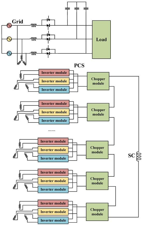
Figure 1.
Topology structure of SMES.
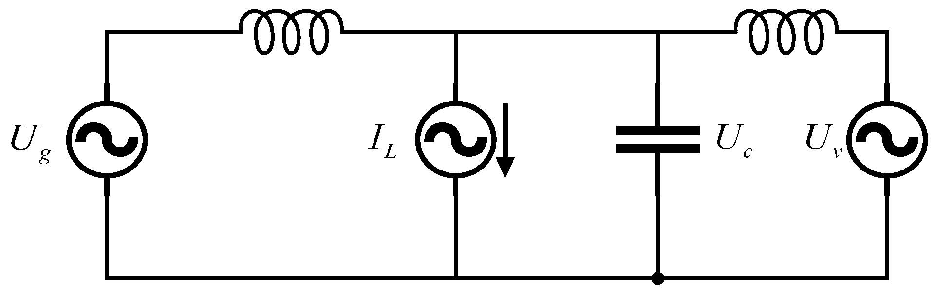
The equivalent circuit is illustrated in Figure 2, where Ug represents the gird and Uc represents grid-side capacitor. The PCS of SMES is represented as the voltage source (Uv), while the load is depicted as the current source (IL). During regular operation, the thyristors are activated. The magnitude and phase of the capacitor voltage are regulated by SMES to manage active and reactive power interchange with the grid. In the event of a grid fault, the thyristors are deactivated. The capacitor voltage is then controlled to maintain its pre-grid fault value, thereby safeguarding the critical load.

Figure 2.
Equivalent circuit diagram of the proposed SMES.
The toroidal SC has the good merit of a low leakage magnetic field, which is more suitable for energy storage. An SC made of YBCO superconductor tape was designed in [28], whose major parameters are listed in Table 1.

Table 1.
Preliminary parameters of the toroidal HTS magnets.
Based on the SC parameters, the SMES PCS design procedure is:
2.1. Select the PCS Rated Voltage
Since the maximum operating current is 1600 A and the total energy stored in the SC is:
where L is the inductance of the SC. The PCS is designed to be able to output the rated power even when the energy storage in the SC drops to 10% of its rated value.
When energy is 10% of the rated value, the current of the SC is:
The SC total rated voltage should satisfy the flowing inequation:
Since the rated PCS is designed to be 5 MW, the should be larger than 10 kV.
2.2. Design of the L Filter Inductance
The inverter module is connected to the secondary side of the transformer through an L filter. The L filter is used to filter out switching harmonics, whose inductance is determined by the maximum allowable current ripple:
where Tsw is the switching period, is the DC link voltage, and is inductance of the L filter. Since phase shift modulation method is used for 8 inverter modules, the total current ripple is 1/8 of a single module. Therefore can be relatively high to save the inductor cost.
2.3. Design of the Capacitance of the DC Link Capacitor
The DC link capacitor is used to filter out the DC link voltage ripples. Since the rated SC current is 1600 A, which is relatively high, the chopper switching frequency is designed to be 1/10 (1000 Hz) of the inverter module to reduce the switching losses. Due to the low switching frequency, the voltage ripple on the DC link is mainly due to the charging and discharging of the DC link capacitor by the SC current through the chopper. The highest DC link voltage ripple occurs when the chopper outputs maximum power. The DC link ripple magnitude can be expressed as:
where Isc represents the rated SC current, Tsc represents the chopper switching period, and D represents the duty cycle.
The chopper output power can be expressed as:
The chopper outputs maximum power when the inverter reaches its rated power. The maximum chopper power is:
where is the PCS rated power, and n is the number of the sets of power modules, which is eight here.
From (5) to (7), we have:
When is taken as 1.5% Udc, C is calculated as about 50 mF.
2.4. Design of the Inductance of the Grid-Side Inductor
When the angle between the grid and capacitor voltage is small enough, the output active power of SMES is linear with :
where represents the grid voltage magnitude, represents the capacitor voltage magnitude, X represents line impedance (, is the grid inductance).
Lg is selected to be 3.2 mH to make maximum less than 0.1.
2.5. Design of the Capacitance of the Grid-Side Capacitor
Since most of the inverter side ripple current flows through the capacitor, voltage fluctuations occur on the capacitor. The capacitance of the capacitor can be selected according to:
where is the maximum voltage ripple, fsw represents the equivalent switching frequency, which is 8 times that of single module with the phase shift modulation.
The capacitance is calculated on the secondary side of the transformer. Since the capacitor is installed on the primary side of the transformer, the capacitance can be calculated as:
According to the above-mentioned parameter calculation method, the parameters of SMES are calculated and listed in Table 2.
Table 2.
Main parameters of SMES.
3. Inverter Outer Power Control Loop
The system control strategy of SMES can be primarily categorized into an outer power loop and an inner voltage and current control loop. The power control loop is primarily utilized for active power smoothing, grid frequency inertial support, and reactive power compensation. Meanwhile, the inner voltage and current loops are predominantly employed for current harmonics and dynamic voltage sag compensation.
3.1. Active Power Loop
The power and frequency control strategy on the grid side employs the virtual synchronous generation (VSG) control method [29,30,31,32]. The outer loop encompasses active power and reactive power control. The model of the synchronous generator can be expressed as:
where J is rotational inertia, is rotor angular velocity, is mechanical power, is electromagnetic power, DP is damping coefficient, is rotor rated angular velocity and θ is power angle.
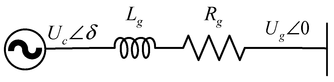
Figure 3 is the equivalent circuit diagram of VSG in grid-connected operation, where represents the grid resistance and represents the grid inductance.

Figure 3.
Equivalent circuit diagram of VSG in grid-connected operation.
The instantaneous power model is used in this paper. The dynamic of the grid inductor current (ig) can be expressed under the d-q reference frame as:
where and are the instantaneous capacitor and grid voltage.
The grid complex power () can be expressed as:
where is the grid inductor current magnitude.
Combining Equations (13) and (14), the dynamic model of is:
The capacitor voltage is controlled to be a steady value, so can be approximately as 0, Equation (15) turns to:
When in the steady case, is expressed as:
Given that the phase angle difference between the grid and capacitor is approximately 0 and the grid resistance can be disregarded, Equation (17) can be simplified as:
where X represents line impedance.
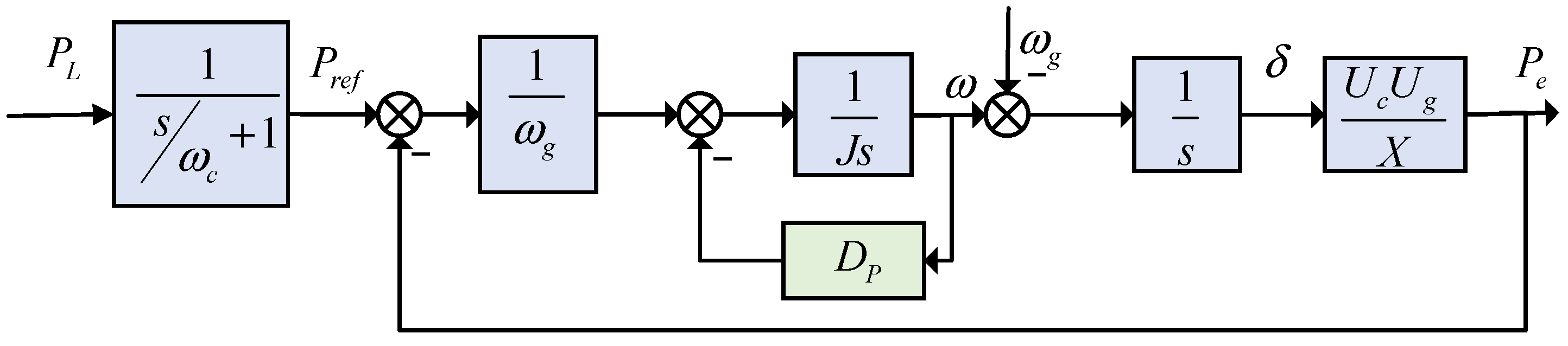
So, the expression of the output active power is as follows:
To smooth the active power of the load, a first-order low-pass filter is applied and utilized as the reference power of VSG. Based on Equations (12) and (19), the block diagram of active power is depicted in Figure 4, where and are the grid frequency and the cutoff frequency of the first-order low-pass filter, respectively.

Figure 4.
Active power control block diagram.
From Equation (20), the VSG-based power loop is a two-order system. The following relation can be obtained:
where refers to natural angular frequency, and refers to the damping ratio.
The damping ratio is designed to be 0.707, so the parameters DP and J have the following relationship:
The formula for the kinetic energy of a rotating object is as follows:
where represents the SMES rated power, t represents energy storage time, and represents the VSG angular velocity. In this paper, is designed to be 5 MW, t is 5 s, and is grid frequency. Therefore, parameter J can be calculated.
As can be seen in Figure 4, there are two inputs in the system, which are the load power and grid frequency . From Figure 4, the grid power can be described as:
In Equation (25), the value of is set to 1 Hz (6.28 rad/s), since ( is 70.7 rad/s from Equation (21)), is the dominant pole of the system. Therefore, the dynamic response of is mainly influenced by the first-order low-pass filter, and the low-pass filter cutoff frequency mainly determines the load active power smoothing performance.
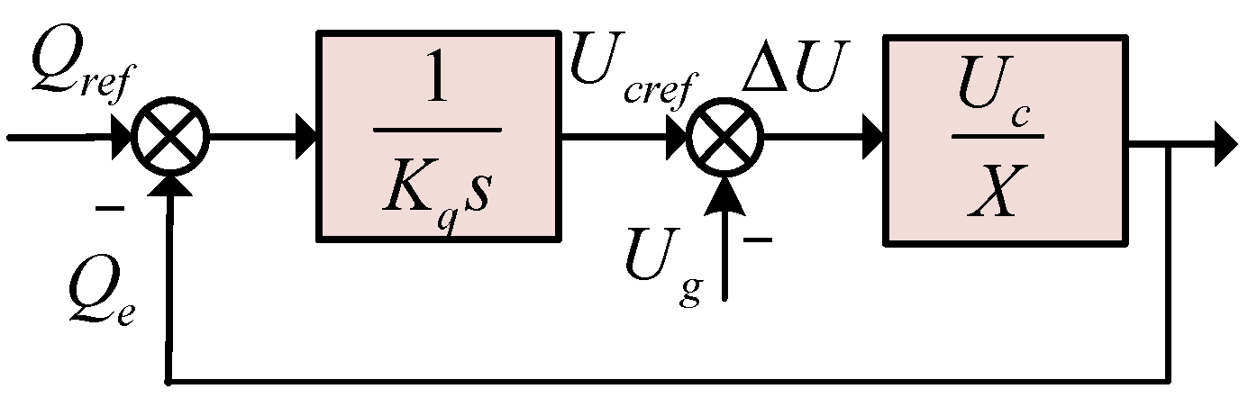
3.2. Reactive Power Loop
To simulate the reactive voltage regulation function of the system, the excitation controller of the VSG achieves control of the output voltage by detecting and managing the system’s output reactive power. To streamline the control process, a first-order inertial link is utilized for modeling. Consequently, the excitation formula of VSG is obtained as:
where Kq is the reactive power–voltage inertia coefficient, Ur is the virtual electromotive force, Qref is the reference reactive power, Qe is the reactive power output. The reference reactive power Qref is set to zero, so the total reactive power of the SMES and load is zero. The reactive power of the load is inherently compensated by the SMES.
From Equation (18), the expression of the output reactive power is as follows:
where is the voltage difference between the capacitor and grid, which can be used to regulate the reactive power.
Based on Equations (27) and (28), the block diagram of reactive power is shown in Figure 5. A simple integral regulator is used, and the final output is the reference value of the capacitor voltage (Ucref).

Figure 5.
Reactive power control block diagram.
The closed-loop transfer function for reactive power control is:
It is clear that is a first-order system, whose bandwidth is:
As evident from Equation (30), the smaller the parameter , the wider the bandwidth of the system, leading to faster response speed.
4. Inverter Inner Voltage and Current Control Loop
4.1. Realization of Voltage Sag Compensation
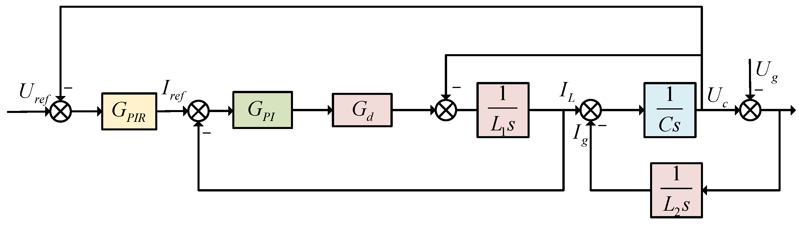
Upon occurrence of a grid fault, the gate signal of the thyristors is deactivated, and the capacitor voltage is regulated to remain unchanged to safeguard the load. A dual-loop control strategy is employed in the capacitor voltage control, comprising inner loop current control and outer loop voltage control, as illustrated in Figure 6. In the diagram, represents the proportional and integral (PI) controller for inner loop current control, represents the proportional, integral, and resonant (PIR) controller for outer loop voltage control. L1 denotes the inverter-side inductance, L2 represents the grid-side inductance, C stands for the grid-side capacitor, Gd indicates the inverter delay, and s represents the Laplace operator. Gd can be expressed as , where Td represents the computational and pulse width modulation delay time of the inverter.
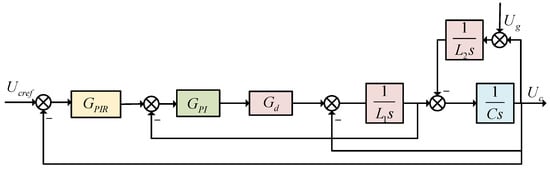
Figure 6.
Inverter module voltage control block diagram.
To design the PI regulator parameters, the PI regulator is written in the zero-pole form as:
where and are the proportional and integral control gains of the inner loop current control, is the time constant corresponding to the zero point in the PI regulator.
The conventional type II system design method is employed to design the inner current loop. From Figure 6, the open-loop transfer function of the inner current loop is:
As observed from Equation (32), there are two parameters to be determined: and , which adds complexity to parameter selection. For ease of analysis, a new variable is introduced. To enhance the control dynamics of the inner current loop while considering overshoot, oscillation amplitude, etc., h is chosen to be 5 as suggested [33]. Given a specific h, the following relationship holds to minimize the peak value of the closed-loop amplitude.
From Equation (33), we have:
When designing the PIR parameters of the outer loop, the PI parameters are first designed. The open-loop transfer function of the outer voltage loop is:
In order not to influence the control of the inner loop, the bandwidth of the outer loop is set to one-third of the inner loop bandwidth and the phase margin is set to 60 degrees. The frequency response of the outer PI controller at the control bandwidth can be expressed as , where refers to the bandwidth of the outer loop, and are the proportional and integral control gains of the outer loop voltage control. The amplitude () and phase angle () of the PI controller transfer function are calculated as and , respectively. To make 60° phase margin, the parameters of the outer loop PI controller can be solved by the following two equations:
where refers to the amplitude of the outer open loop transfer function, and refers to the phase angle of the outer open loop transfer function.
The resonant controller is primarily designed to enhance 5th and 7th order harmonic tracking performance, with its resonant frequency being 6th order in the d-q reference frame. The expression of the resonant controller is as follows:
where represents resonant gain, represents resonant bandwidth, and represents resonant frequency. In this paper, the resonant frequency is chosen to be six times the fundamental frequency to simultaneously suppress the 5th and 7th order harmonics. The gain of the resonance controller is set to be as large as possible to enhance harmonic tracking performance, provided the phase angle margin exceeds 30 degrees. By setting the resonance gain to 2 and the resonance bandwidth to 0.5 times the fundamental frequency, the phase angle margin is calculated as 39.4 degrees, fulfilling the design criteria.
The expression of PIR is shown below:
4.2. Realization of Current Harmonic Compensation
To validate the harmonic current compensation performance, impedance analysis method is used [34].
The dual loop control diagram is shown in Figure 7.
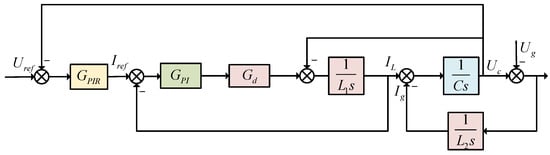
Figure 7.
Control diagram of the capacity voltage.
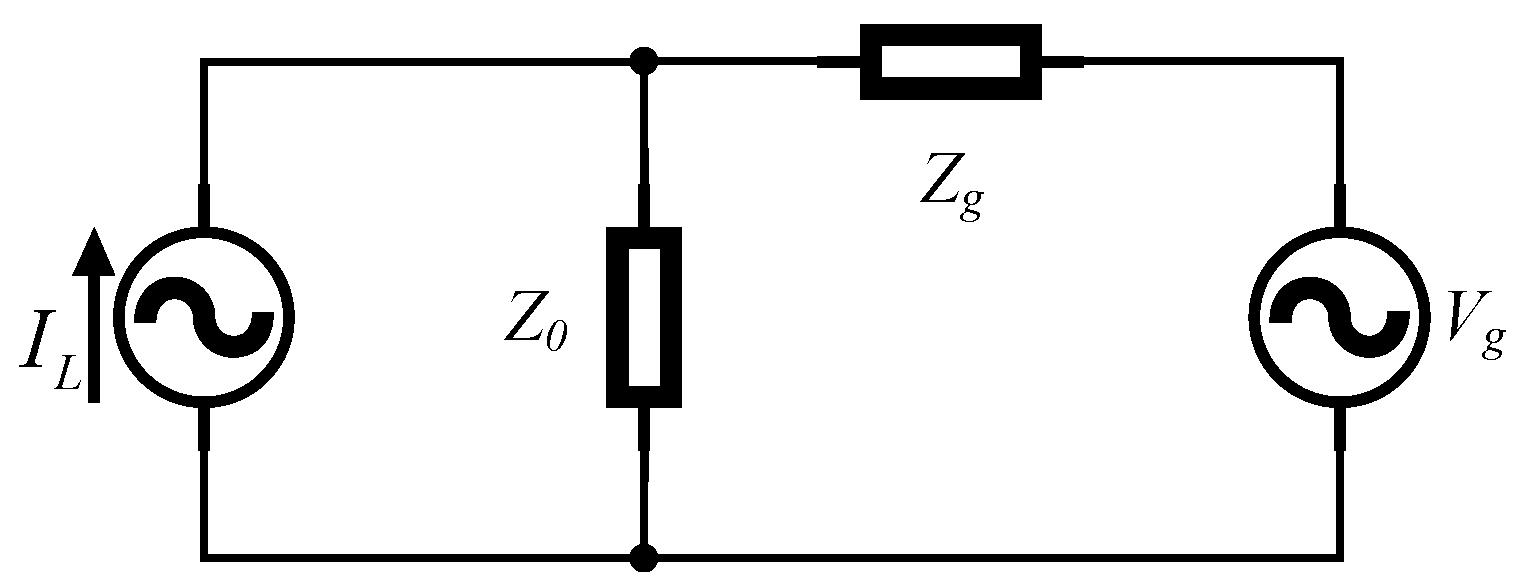
With the impedance modeling method, the inverter is represented by the inverter parallel output impedance , the utility grid is modeled by the voltage source and the grid impedance , the grid is modeled as voltage source Vg, and the load is modeled as a current source IL. The equivalent circuit is shown in Figure 8.

Figure 8.
Equivalent model.
To simplify the impedance analysis, a series of equivalent transformations are performed, which transfers the control diagram in Figure 7 into the ones shown in Figure 9.
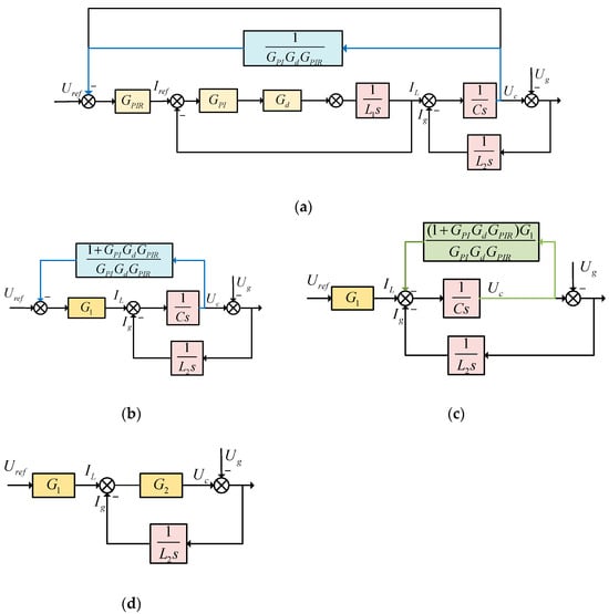
Figure 9.
Simplified block diagram: (a) the first step, (b) the second step, (c) the third step, and (d) the fourth step.
Step 2: Merge the two feedback loops in Figure 9a into , and merge the current inner loop into , yielding Figure 9b.
The resulting transfer function of G1(s) and G2(s) can be expressed by:
The output impedance of the inverter and grid can be defined as:
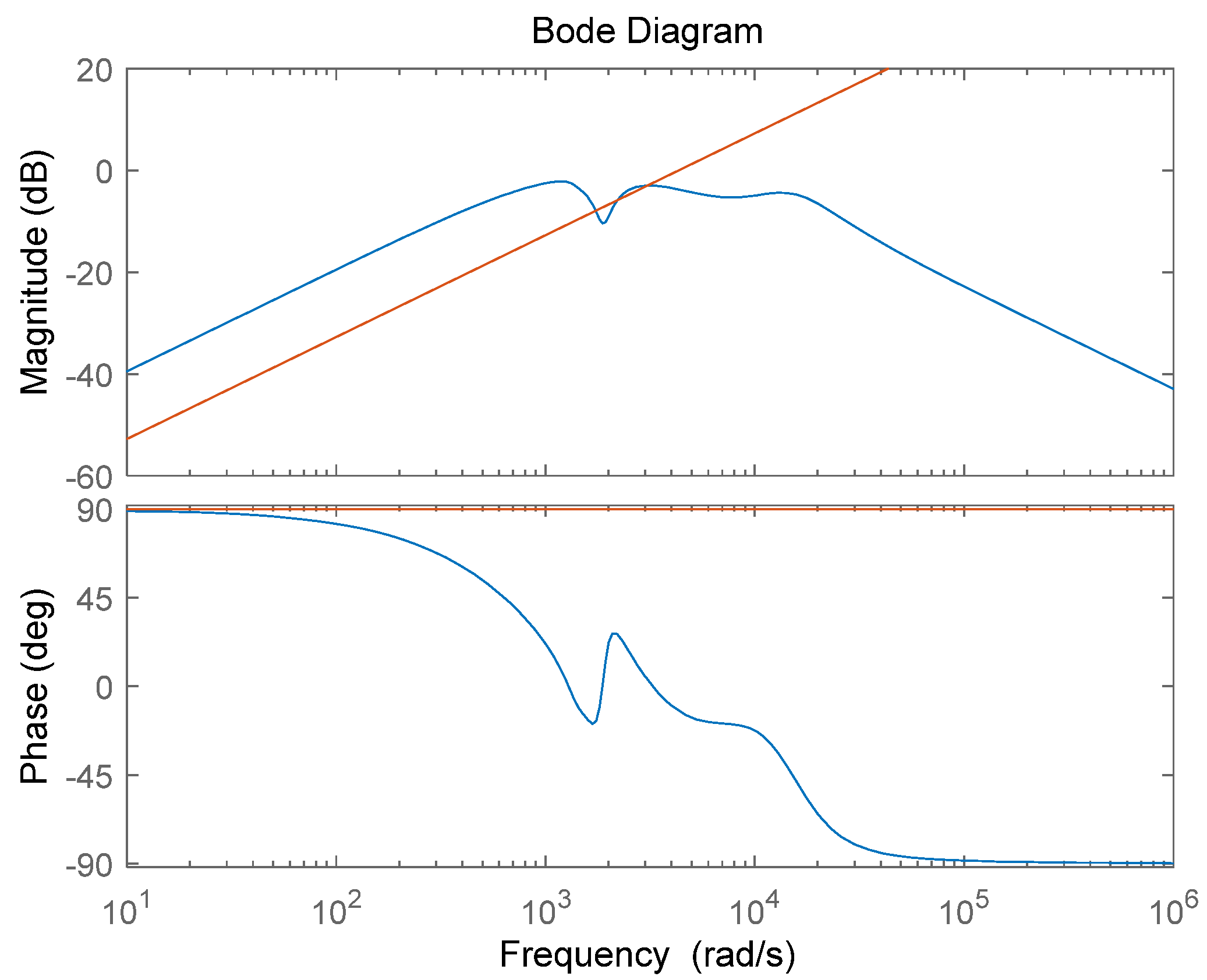
Based on Equations (42) and (43), the following bode diagram is plotted (Figure 10), where the blue and red lines are the impedance of Z0 and Zg, respectively.
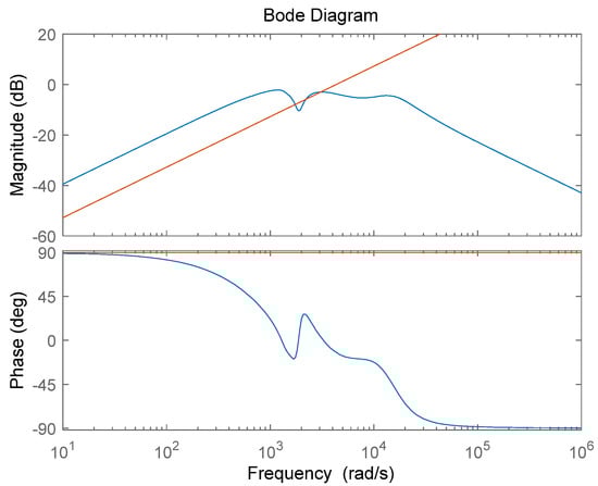
Figure 10.
Bode diagram of Z0 and Zg.
As depicted in the figure, in the high-frequency domain, the harmonic impedance of the grid notably exceeds that of the inverter. Consequently, the majority of harmonic current will flow into the inverter rather than the grid, enabling the realization of the harmonic current compensation function.
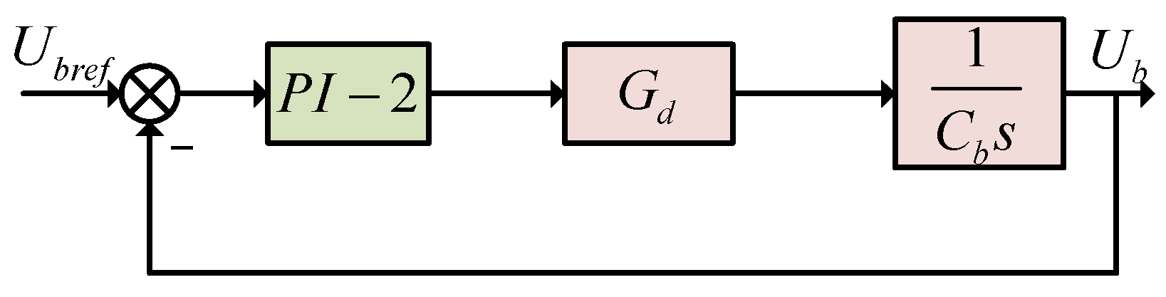
5. Chopper Module Control
The chopper module is mainly designed to control the DC bus voltage, and its control block diagram is as follows Figure 11.
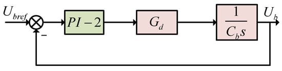
Figure 11.
Chopper module control block diagram.
Where PI-2 represents the PI controller for voltage control, Cb represents the DC capacitor, Ubref represents the reference DC link voltage and Ub represents the DC link voltage.
According to the typical type II system design method, which is mentioned in the preceding paragraph, the parameters of the PI-2 controller are designed as follows:
where and are the proportional and integral control gains of chopper.
6. Simulation Results
Simulations are conducted to showcase the system’s performance in inertia support, active current harmonics filtering, reactive power compensation, active power smoothing, and dynamic voltage sag compensation.
Figure 12 illustrates the waveform of the active power absorbed from the grid following a 0.1 Hz grid frequency step increment. As the grid frequency undergoes a sudden change, the phase angle difference between the grid and the inverter experiences a significant increase. Consequently, the SMES absorbs step active power to mitigate the grid frequency change, thereby providing inertia support.

Figure 12.
Effect of inertial support.
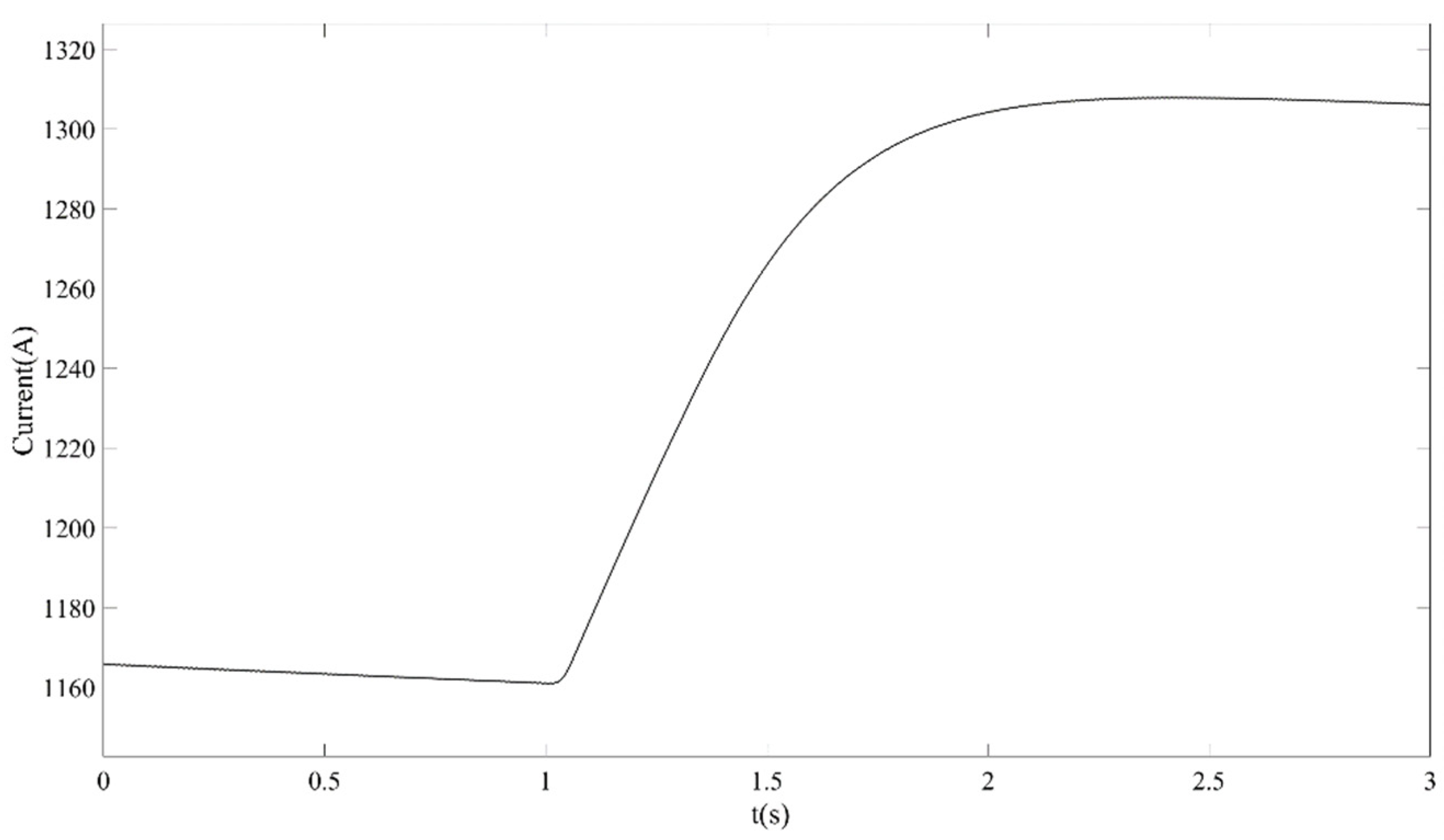
Figure 13 displays the waveform of SC current in inertia support. At 0–1 s, active power smoothing has a transient process when it has just started and has not yet entered the steady state. At this time, the load power is slightly greater than the power absorbed from the grid, so SMES provide energy for the load and the SC current slowly decreases. At one second, the active power emitted by the grid notably escalates, while the active power of the load remains approximately constant at 2 MW. Consequently, the SMES absorbs power from the grid, causing the current of the SC to rise. Between approximately 1.1 and 2.5 s, the active power emitted by the grid gradually diminishes but remains higher than that of the load. Consequently, the power absorbed by the SMES from the grid decreases, while the SC current continues to increase at a decreasing rate. After 2.5 s, the active power of the grid and the load almost equalize, resulting in a stable SC current.

Figure 13.
SC’s current in inertial support.
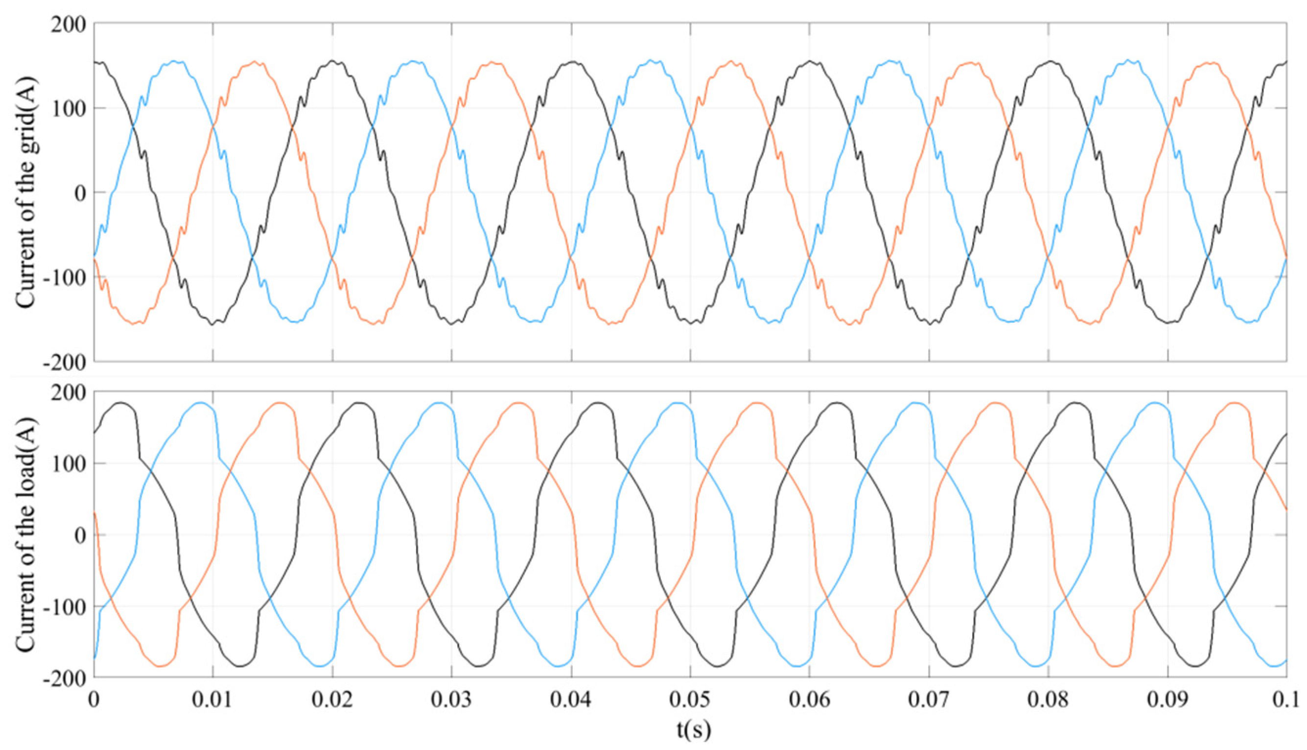
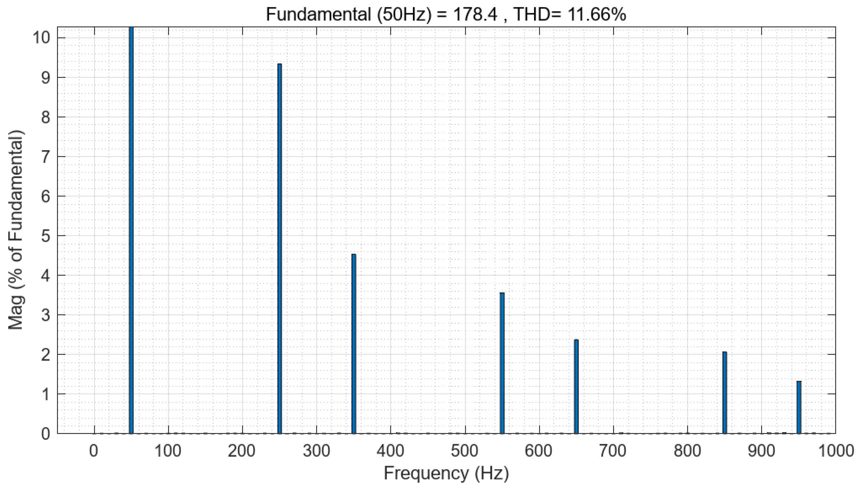
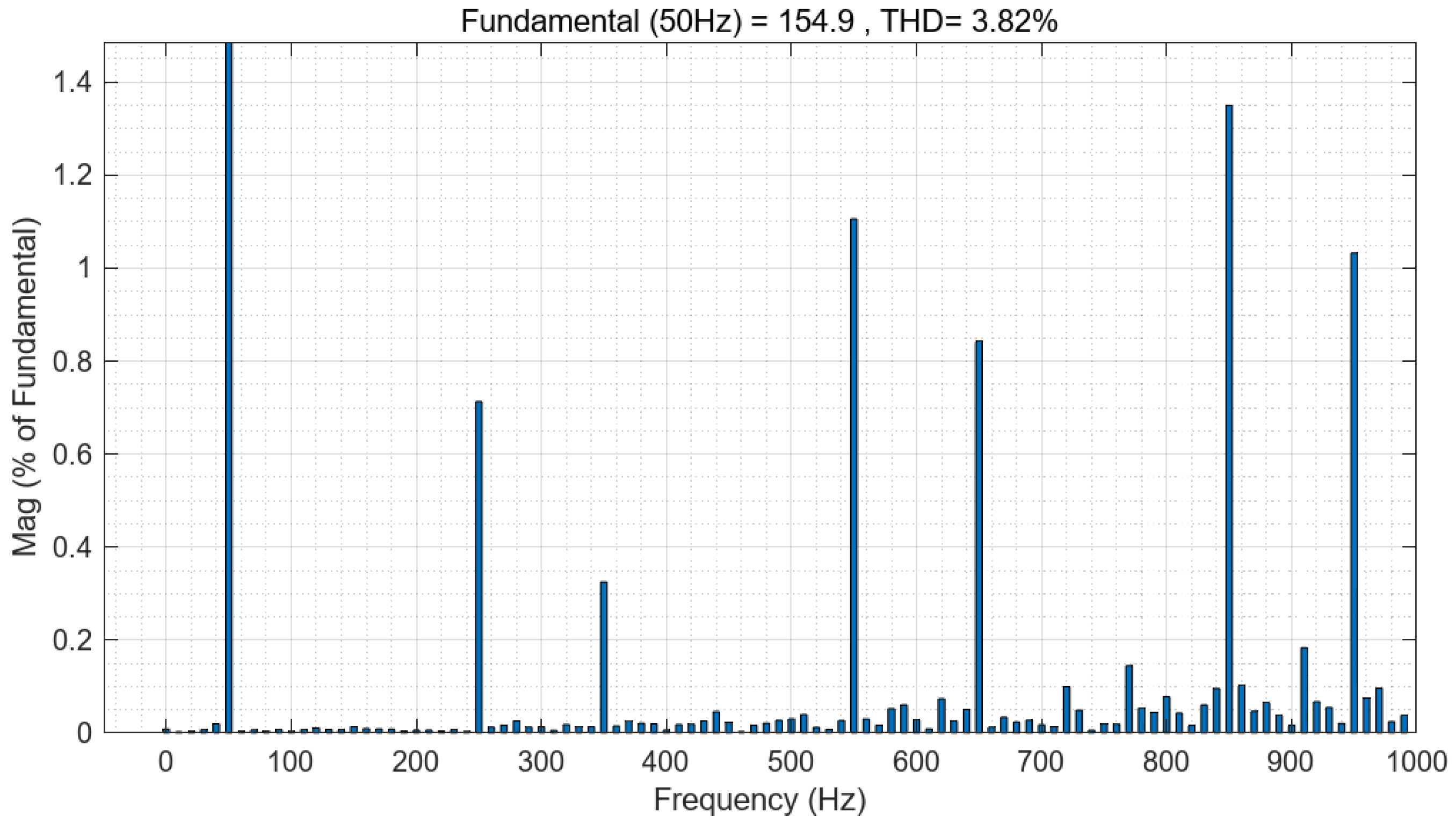
Figure 14 illustrates the impact of current harmonic compensation. The upper half of the figure presents the waveform of the grid current after filtering, while the lower half displays the current waveform of the load. Nonlinear loads within the load result in noticeable harmonic distortions. Figure 15 shows the harmonic distortion rate of load current and Figure 16 shows the harmonic distortion rate of grid current. The total harmonic distortion (THD) of the load current is as high as 11.66%, failing to meet the fundamental requirements of the grid. However, following active filtering of the load current, the grid harmonic distortion is reduced to 3.82%, meeting the stipulated grid code requirements.
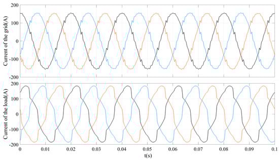
Figure 14.
Effect of active filtering.
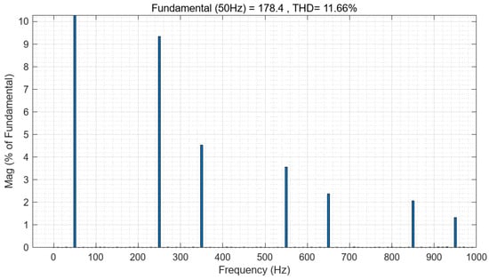
Figure 15.
Harmonic distortion rate of load current.
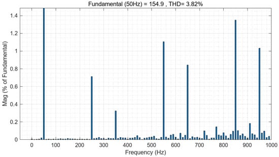
Figure 16.
Harmonic distortion rate of grid current.
Figure 17 depicts the simulation waveform for reactive power compensation. The magenta line represents the reactive power of the load, while the blue line illustrates the reactive power of the grid. A step change in load power occurs between 1 and 2 s. Owing to the presence of harmonics, the reactive power of the grid exhibits significant fluctuations. Following compensation, the average reactive power injected into the grid is reduced to 0. The fluctuation in reactive power is significantly dampened due to current harmonic compensation. By greatly reducing the harmonic content, the fluctuation amplitude of the reactive power is diminished. Upon a step power change in the load, there is a slight transient oscillation in the reactive current injected into the grid. However, it quickly diminishes to 0, indicating rapid reactive power regulation speed within the system.
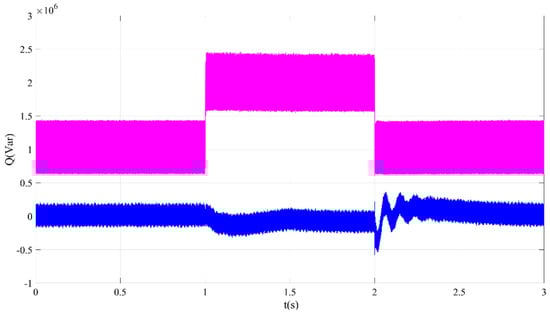
Figure 17.
Effect of reactive power compensation.
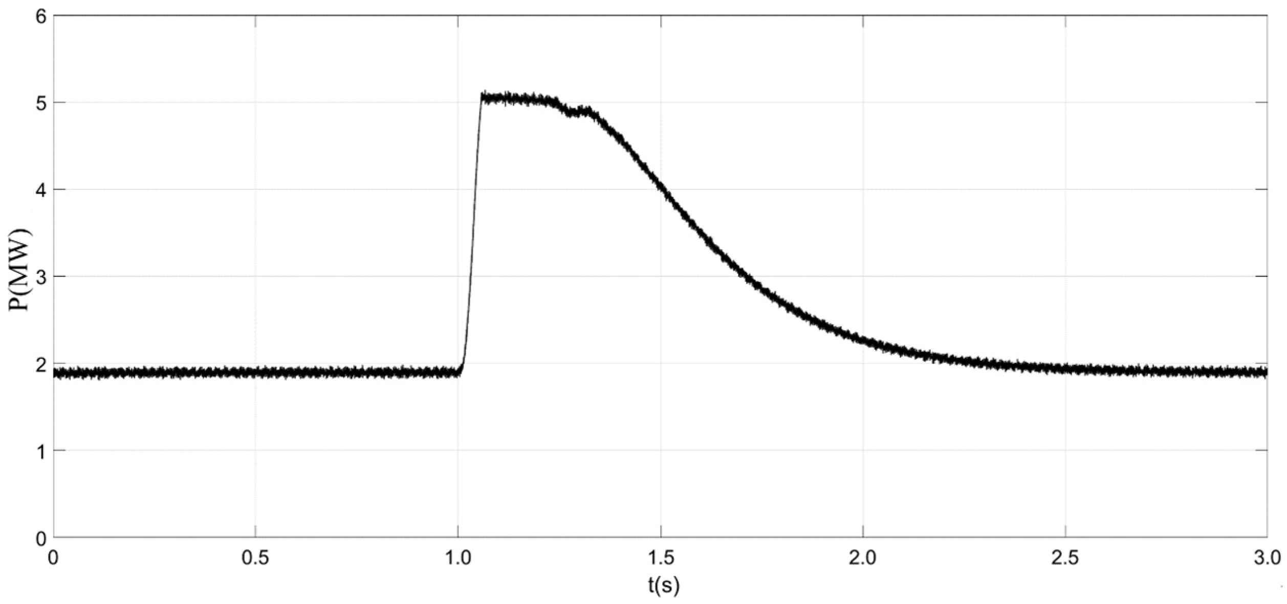
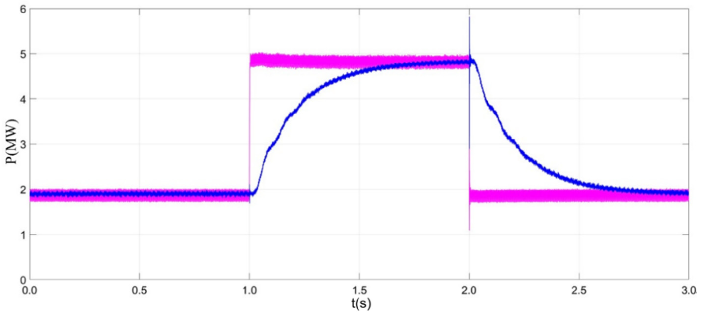
Figure 18 and Figure 19 display the simulation waveforms of active power smoothing. In Figure 18, the magenta curve represents the active power of the load, which jumps from 2 MW to 5 MW in 1 s and returns to 2 MW in 2 s. The blue curve depicts the active power provided by the grid. Despite the step change in the load’s active power, the active power supplied by the grid remains much smoother, effectively mitigating the impact of dynamic load fluctuations on the grid. Figure 19 illustrates the current waveforms of the load and the grid during the step process. It is evident that the rate of change in the grid current waveform is much lower than that of the load, thereby reducing the impact on the grid.

Figure 18.
Effect of active power smoothing.
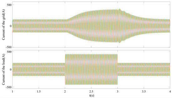
Figure 19.
Waveform of grid and load currents in active power smoothing.
Figure 20 illustrates the SC’s current waveform during active power smoothing. Between 1 and 2 s, the load’s power remains at 5 MW, while the grid’s power gradually increases from 2 MW to 5 MW. Consequently, the SMES provides power for the load, resulting in a decrease in SC current. Between 2 and 3 s, the load’s power is 2 MW, while the grid’s power decreases from 5 MW to 2 MW. In this scenario, the SMES absorbs the differential power, causing the SC current to rise.
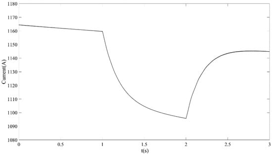
Figure 20.
SC’s current in active power smoothing.
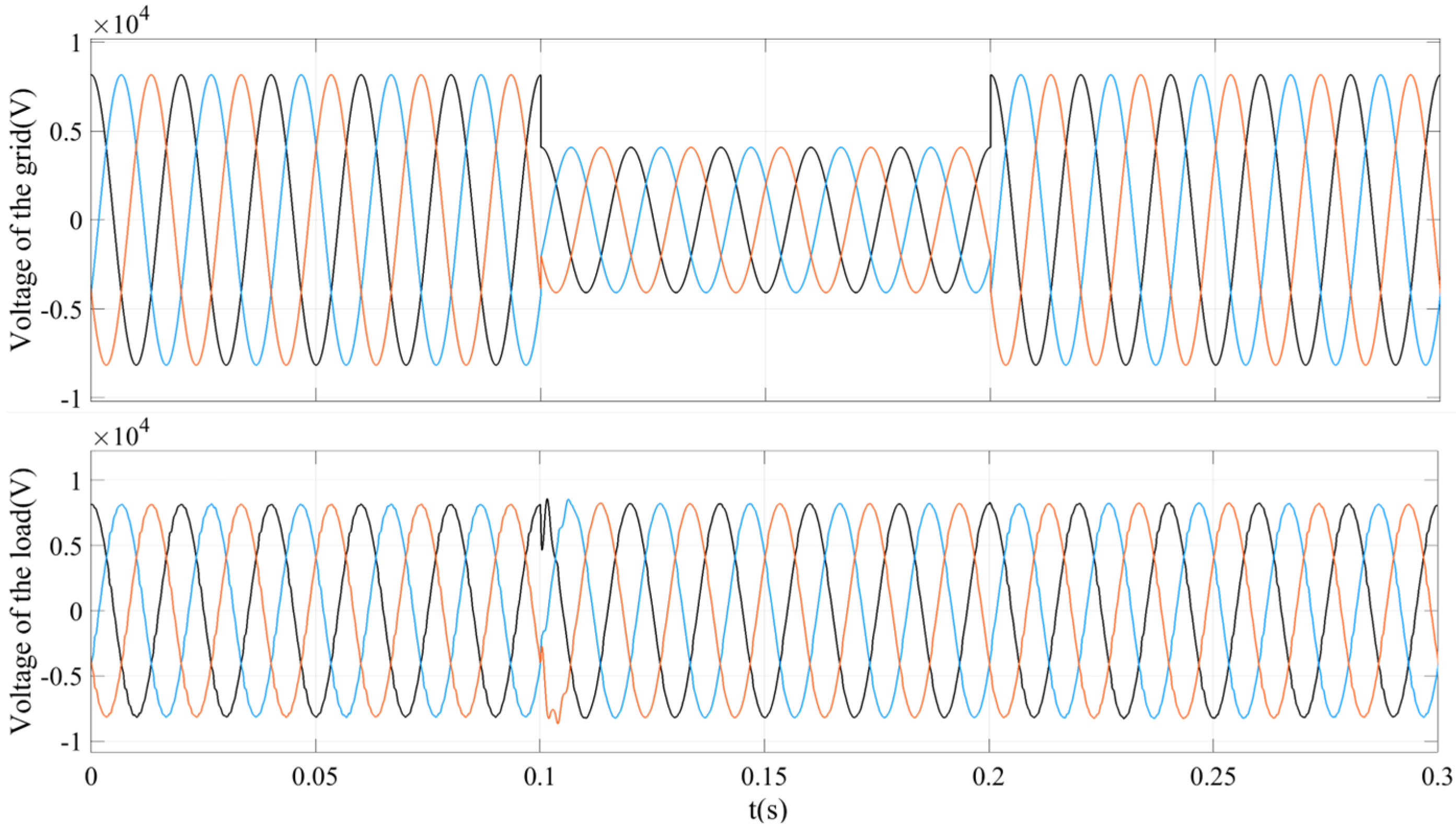
Figure 21 illustrates the simulation waveform during a voltage sag event. Between 0.1 and 0.2 s, the amplitude of the grid voltage decreases to 50% of the normal value. Upon detection of the grid fault, the thyristors are turned off. SMES supports the load voltage by controlling the capacitor voltage to match the value before the grid fault. Consequently, the amplitude of the load voltage remains unchanged, with only a minor disturbance observed during the sudden grid voltage sag, effectively realizing the critical load protection function.
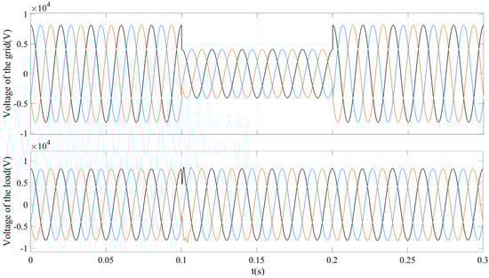
Figure 21.
Effect of dynamic voltage transient management.
Figure 22 and Figure 23 display the active power and the SC’s current waveform during this process. In Figure 22, the magenta line represents the active power of the load, while the blue line indicates the active power of the grid. At 0.1 s, the thyristors are deactivated, causing the grid power to sharply decrease to 0. Consequently, SMES supplies power to the load, resulting in a decrease in SC current (as shown in Figure 23). At 0.2 s, the grid fault is cleared, and the thyristors are reactivated to reconnect SMES and the load with the grid. Following this, the active power of the load remains unchanged, while the active power provided by the grid gradually increases but remains lower than the power of the load. Therefore, SMES needs to provide compensational power for the load. Since the VSG-controlled SMES requires a transient process to follow the reference value (which is the first-order filtered load power), the load power gradually transitions from being provided by SMES to being provided by the grid. Consequently, the SC current continues to decrease at a decreasing rate.
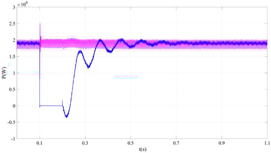
Figure 22.
Active power of the grid and load in dynamic voltage transient management.
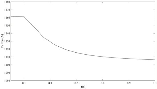
Figure 23.
SC’s current in dynamic voltage transient management.
7. Performance Comparison with the Existing Methods
Table 3 lists the applications and functions of SEMS devices in recent years. It can be seen that most SMES devices can only achieve 1–2 functions, and none of them have all the functions listed in the table, resulting in low cost-effectiveness and low utilization rate of SMES devices. The SMES equipment proposed in this paper has all the functions, which greatly improve the equipment’s utilization rate.
Table 3.
Functional comparison of SMES devices.
8. Conclusions
In this paper, a multi-functional device based on SMES is explored, which not only bolsters the stability of the power system but also notably enhances power quality. The proposed approach enables the realization of grid frequency support, active power smoothing, and reactive power compensation functions through the outer power control loop. Additionally, the inner voltage and current control loops facilitate the realization of grid voltage sag and harmonic current compensation functions. By integrating multiple functions into a single equipment, the cost-effectiveness of SMES can be substantially enhanced. Simulation results validate the effectiveness of the proposed approaches.
Author Contributions
Conceptualization, W.G.; methodology, W.G.; software, W.G. and Y.H.; validation, W.G. and Y.H.; formal analysis, Y.H.; investigation, Y.H.; resources, W.G.; data curation, Y.H.; writing—original draft, Y.H.; writing—review and editing, W.G. and Y.H.; visualization, Y.H., J.L. and Y.Y.; supervision, J.L. and Y.Y.; project administration, J.L. and Y.Y.; funding acquisition, J.L. and Y.Y. All authors have read and agreed to the published version of the manuscript.
Funding
This research was funded by the Fundamental Research Funds for the Central Universities under grant 2022XKRC018.
Data Availability Statement
The original contributions presented in the study are included in the article, further inquiries can be directed to the corresponding author.
Acknowledgments
We would like to thank J. Lan, Y. Yang. and W. Liu for their valuable contributions to this research. We gratefully acknowledge the Center for Superconductivity of BJTU for providing the necessary equipment for this study. We would also like to thank our families for their constant support and encouragement throughout this research.
Conflicts of Interest
The authors declare no conflicts of interest.
References
- AL Shaqsi, A.Z.; Sopian, K.; Al-Hinai, A. Review of energy storage services, applications, limitations, and benefits. Energy Rep. 2020, 6, 288–306. [Google Scholar] [CrossRef]
- Sonia; Dahiya, A.K. Superconducting magnetic energy storage coupled static compensator for stability enhancement of the doubly fed induction generator integrated system. J. Energy Storage 2021, 44, 103232. [Google Scholar] [CrossRef]
- Chen, X.; Zhang, M.; Jiang, S.; Gou, H.; Zhou, P.; Yang, R.; Shen, B. Energy reliability enhancement of a data center/wind hybrid DC network using superconducting magnetic energy storage. Energy 2023, 263, 125622. [Google Scholar] [CrossRef]
- Nam, G.D.; Sung, H.J.; Go, B.S.; Park, M.; Yu, I.K. Design and Comparative Analysis of MgB2 and YBCO Wire-Based-Superconducting Wind Power Generators. IEEE Trans. Appl. Supercond. 2018, 28, 1–5. [Google Scholar] [CrossRef]
- Zhang, H.; Lin, D.; Wang, D.; Shi, J.; Zhu, B.; Ma, S.; Zhang, M.; Pan, Y. Design and control of a new power conditioning system based on superconducting magnetic energy storage. J. Energy Storage 2022, 51, 104359. [Google Scholar] [CrossRef]
- Ren, J.; Xiao, X.; Zheng, Z. In Application of CSC-based SMES to Improve the LVRT Capability of DFIG-based WECS. In Proceedings of the 2020 IEEE International Conference on Applied Superconductivity and Electromagnetic Devices (ASEMD), Tianjin, China, 16–18 October 2020; pp. 1–2. [Google Scholar]
- Adetokun, B.B.; Oghorada, O.; Abubakar, S.J. Superconducting magnetic energy storage systems: Prospects and challenges for renewable energy applications. J. Energy Storage 2022, 55, 105663. [Google Scholar] [CrossRef]
- Zhou, A.; Shi, J.; Dai, Q.; Zhang, Z.; Xia, Z.; Zhou, X.; Zhang, C.; Tang, Y. The Supplementary Design Method of HTS SMES System Considering Voltage Distribution Characteristic. IEEE Trans. Appl. Supercond. 2017, 27, 1–5. [Google Scholar] [CrossRef]
- Shi, J.; Lin, D.; Liao, M.; Yang, W.; Zhang, Z.; Zou, X.; Xu, Y.; Ren, L. The Influence of SMES Magnet Operation Parameters on Voltage Distribution Characteristic. IEEE Trans. Appl. Supercond. 2022, 32, 1–5. [Google Scholar] [CrossRef]
- Xiao, L.; Dai, S.; Lin, L.; Zhang, J.; Guo, W.; Zhang, D.; Gao, Z.; Song, N.; Teng, Y.; Zhu, Z.; et al. Development of the World’s First HTS Power Substation. IEEE Trans. Appl. Supercond. 2012, 22, 5000104. [Google Scholar] [CrossRef]
- Dai, S.; Xiao, L.; Wang, Z.; Guo, W.; Zhang, J.; Zhang, D.; Gao, Z.; Song, N.; Zhang, Z.; Zhu, Z.; et al. Development and Demonstration of a 1 MJ High-Tc SMES. IEEE Trans. Appl. Supercond. 2012, 22, 5700304. [Google Scholar]
- Ren, L.; Xu, Y.; Zuo, W.; Shi, X.; Jiao, F.; Liu, Y.; Deng, J.; Li, J.; Shi, J.; Wang, S.; et al. Development of a Movable HTS SMES System. IEEE Trans. Appl. Supercond. 2015, 25, 1–9. [Google Scholar] [CrossRef]
- Liu, W.; Dai, S.; Ma, T.; Shi, Y. Voltage Distribution Characteristic of the D-Shaped Coil of HTS-SMES under High-Frequency Impulse. IEEE Trans. Appl. Supercond. 2022, 32, 1–10. [Google Scholar] [CrossRef]
- Jose, P.A.; Deepak, M. In Fast Frequency Support from Doubly Fed Induction Generators in Coordination with Super-conducting Magnetic Energy Storage Systems. In Proceedings of the 2022 IEEE International Conference on Power Electronics, Smart Grid, and Renewable Energy (PESGRE), Trivandrum, India, 2–5 January 2022; pp. 1–6. [Google Scholar]
- Shi, J.; Tang, Y.; Xia, Y.; Ren, L.; Li, J.; Jiao, F. Energy Function Based SMES Controller for Transient Stability Enhancement. IEEE Trans. Appl. Supercond. 2012, 22, 5701304. [Google Scholar]
- Shi, J.; Zhou, A.; Liu, Y.; Ren, L.; Tang, Y.; Li, J. Voltage Distribution Characteristic of HTS SMES Magnet. IEEE Trans. Appl. Supercond. 2016, 26, 1–5. [Google Scholar] [CrossRef]
- Alsharif, A.; Khalid, M. In PV/Fuel Cell/ Superconducting Magnetic Energy Storage Coupled with VSG to Improve Frequency and Voltage Regulation of Power Grid. In Proceedings of the 2023 IEEE PES GTD International Conference and Exposition (GTD), Istanbul, Turkiye, 22–25 May 2023; pp. 350–355. [Google Scholar]
- Salama, H.S.; Said, S.M.; Vokony, I.; Hartmann, B. Adaptive Coordination Strategy Based on Fuzzy Control for Electric Vehicles and Superconducting Magnetic Energy Storage—Towards Reliably Operating Utility Grids. IEEE Access 2021, 9, 61662–61670. [Google Scholar] [CrossRef]
- Malla, S.G.; Al Jaafari, K.; Al Hosani, K.; Muduli, U.R. In Improvement of Power Quality through SMES Control in a Standalone Hybrid Microgrid System. In Proceedings of the 2023 IEEE IAS Global Conference on Emerging Technologies (GlobConET), London, UK, 19–21 May 2023; pp. 1–6. [Google Scholar]
- Song, M.; Shi, J.; Liu, Y.; Xu, Y.; Hu, N.; Tang, Y.; Ren, L.; Li, J. 100 kJ/50 kW HTS SMES for Micro-Grid. IEEE Trans. Appl. Supercond. 2015, 25, 1–6. [Google Scholar] [CrossRef]
- Nguyen, T.T.; Yoo, H.J.; Kim, H.M. Applying Model Predictive Control to SMES System in Microgrids for Eddy Current Losses Reduction. IEEE Trans. Appl. Supercond. 2016, 26, 1–5. [Google Scholar] [CrossRef]
- Guo, W.; Xiao, L.; Dai, S. Enhancing Low-Voltage Ride-Through Capability and Smoothing Output Power of DFIG with a Superconducting Fault-Current Limiter–Magnetic Energy Storage System. IEEE Trans. Energy Convers. 2012, 27, 277–295. [Google Scholar] [CrossRef]
- Guo, W.; Zhang, J.; Song, N.; Gao, Z.; Ma, T.; Zhu, Z.; Xu, X.; Li, L.; Wang, Y.; Dai, S.; et al. Overview and Development Progress of a 1-MVA/1-MJ Superconducting Fault Current Limiter-Magnetic Energy Storage System. IEEE Trans. Appl. Supercond. 2016, 26, 1–5. [Google Scholar]
- Xie, Q.; Zheng, Z.; Xiao, X.; Huang, C.; Zheng, J.; Ren, J. Enhancing HVRT capability of DFIG-based wind farms using cooperative rotor-side SMES considering the blocking fault of LCC-HVDC system. CSEE J. Power Energy 2021, 7, 698–707. [Google Scholar]
- Jin, J.X.; Xu, W.; Chen, X.Y.; Zhou, X.; Zhang, J.Y.; Gong, W.Z.; Ren, A.L.; Xin, Y. In Developments of SMES devices and potential applications in smart grids. In Proceedings of the IEEE PES Innovative Smart Grid Technologies, Tianjin, China, 21–24 May 2012. [Google Scholar]
- Amaro, N.; Pina, J.M.; Martins, J.; Ceballos, J.M. In Integration of SMES devices in power systems—Opportunities and challenges. In Proceedings of the 2015 9th International Conference on Compatibility and Power Electronics (CPE), Costa da Caparica, Portugal, 24–26 June 2015. [Google Scholar]
- Chen, X.Y.; Jin, J.X.; Xin, Y.; Shu, B.; Tang, C.L.; Zhu, Y.P.; Sun, R.M. Integrated SMES Technology for Modern Power System and Future Smart Grid. IEEE Trans. Appl. Supercond. 2014, 24, 1–5. [Google Scholar] [CrossRef]
- Liu, W.; Dai, S.; Ma, T.; Shi, Y.; Song, M.; Xia, Y. Longitudinal Insulation Design of Hybrid Toroidal Magnet for 10 MJ High-Temperature Superconducting Magnetic Energy Storage. IEEE Trans. Dielectr. Electr. Insul. 2024, 31, 366–375. [Google Scholar] [CrossRef]
- Li, J.; Wen, B.; Wang, H. Adaptive Virtual Inertia Control Strategy of VSG for Micro-Grid Based on Improved Bang-Bang Control Strategy. IEEE Access 2019, 7, 39509–39514. [Google Scholar] [CrossRef]
- Wang, Q.; Zhou, D.; Yin, S.; Lei, Y.; He, T. In Improved Adaptive Inertia and Damping Coefficient Control Strategy of VSG Based on Optimal Damping Ratio. In Proceedings of the 2022 International Power Electronics Conference (IPEC-Himeji 2022-ECCE Asia), Himeji, Japan, 15–19 May 2022; pp. 102–107. [Google Scholar]
- Xu, J.; Wang, J.; Li, K.; Gui, X.; Liu, Q.; Jiang, G.; Xue, J. In A New Adaptive Frequency Control Strategy for VSG Based on Grid Forming Converter of Renewable Energy. In Proceedings of the 2023 Power Electronics and Power System Conference (PEPSC), Hangzhou, China, 24–26 November 2023; pp. 53–60. [Google Scholar]
- Quan, X.; Yu, R.; Zhao, X.; Lei, Y.; Chen, T.; Li, C.; Huang, A.Q. Photovoltaic Synchronous Generator: Architecture and Control Strategy for a Grid-Forming PV Energy System. IEEE J. Emerg. Sel. Top. Power Electron. 2020, 8, 936–948. [Google Scholar] [CrossRef]
- Zhang, X.; Zhang, C. PWM Rectifier and Its Control; China Machine Press: Beijing, China, 2012. [Google Scholar]
- Jiao, J.; Nelms, R.M. In Regulating output impedance using a PI controller to improve the stability of a single phase inverter under weak grid. In Proceedings of the 2016 IEEE 16th International Conference on Environment and Electrical Engineering (EEEIC), Florence, Italy, 7–10 June 2016; p. 1. [Google Scholar]
- Guo, W.; Xiao, L.; Dai, S.; Lin, L. Control Strategy of a 0.5 MVA/1 MJ SMES Based Dynamic Voltage Restorer. IEEE Trans. Appl. Supercond. 2010, 20, 1329–1333. [Google Scholar]
- Guo, W.; Zhang, G.; Zhang, J.; Song, N.; Gao, Z.; Xu, X.; Jing, L.; Teng, Y.; Zhu, Z.; Xiao, L. Development of a 1-MVA/1-MJ Superconducting Fault Current Limiter–Magnetic Energy Storage System for LVRT Capability Enhancement and Wind Power Smoothing. IEEE Trans. Appl. Supercond. 2018, 28, 1–5. [Google Scholar] [CrossRef]


Disclaimer/Publisher’s Note: The statements, opinions and data contained in all publications are solely those of the individual author(s) and contributor(s) and not of MDPI and/or the editor(s). MDPI and/or the editor(s) disclaim responsibility for any injury to people or property resulting from any ideas, methods, instructions or products referred to in the content. |
© 2024 by the authors. Licensee MDPI, Basel, Switzerland. This article is an open access article distributed under the terms and conditions of the Creative Commons Attribution (CC BY) license (https://creativecommons.org/licenses/by/4.0/).