
Simulation and Comparison of the Photovoltaic Performance of Conventional and Inverted Organic Solar Cells with SnO2 as Electron Transport Layers


Abstract
:1. Introduction
2. Methods
2.1. Governing Equations
2.2. Evaluation of the Performance Indicators

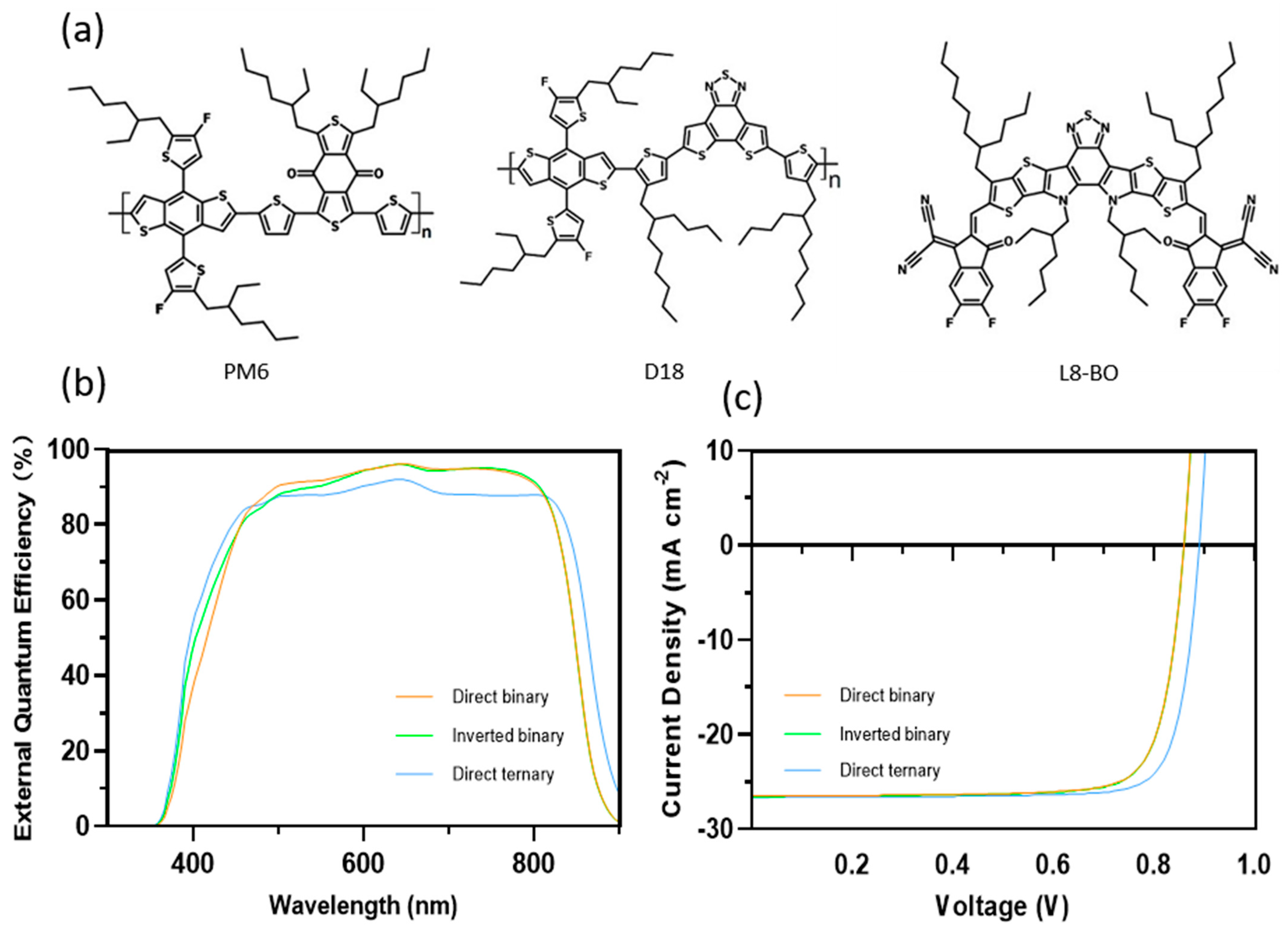
| Reference | Structure | Voc (v) | Jsc (mA/cm2) | FF (%) | PCE (%) |
|---|---|---|---|---|---|
| Rafiq et al. [47] | ITO/MoO3/PDTS-DTTFBT:PC71BM/C60/PC60BM/ZnO/Ag | 0.999 | 20.01 | 88.52 | 17.69% |
| Ram et al. [48] | ITO/WS2/PBDB-T-2F:Y6:PC71BM/PFN-Br/Al | 0.85 | 25.1 | 80 | 17.10% |
| Zhu et al. [14] | ITO/PEDOT:PSS/PM6:D18:L8-BO/PNDIT-F3N/Ag | 0.87 | 24.49 | 80.38 | 17.21% |
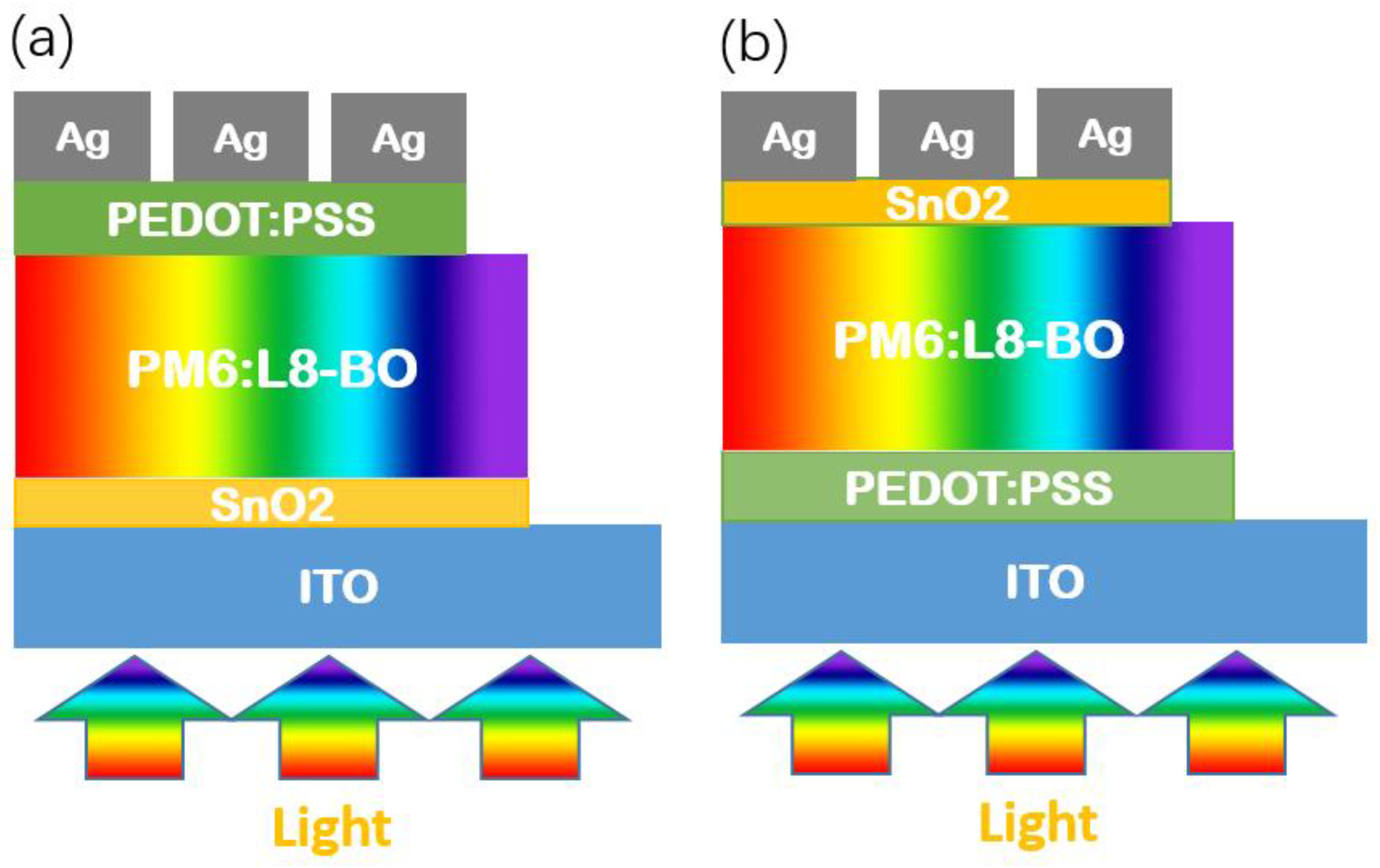
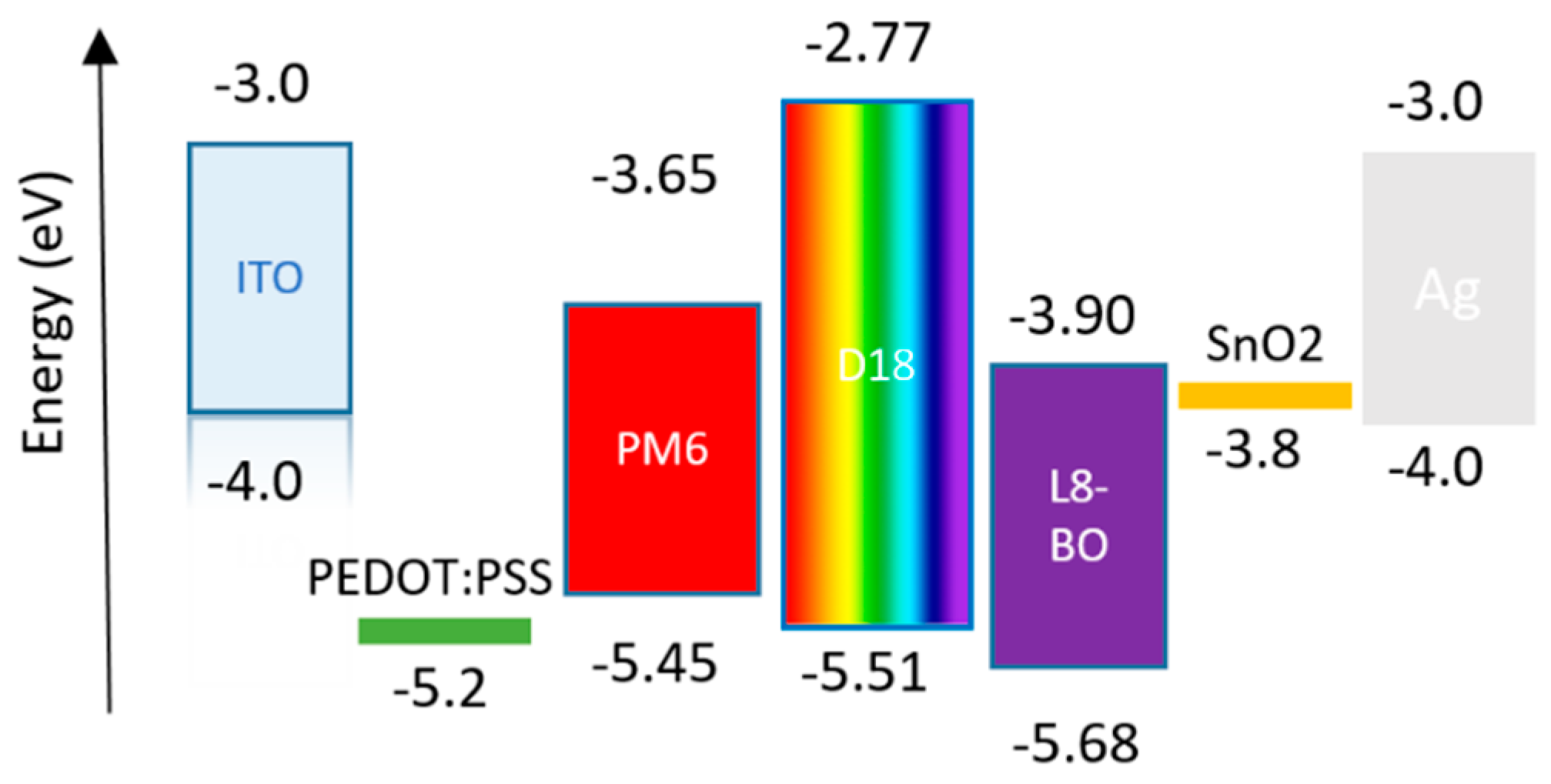
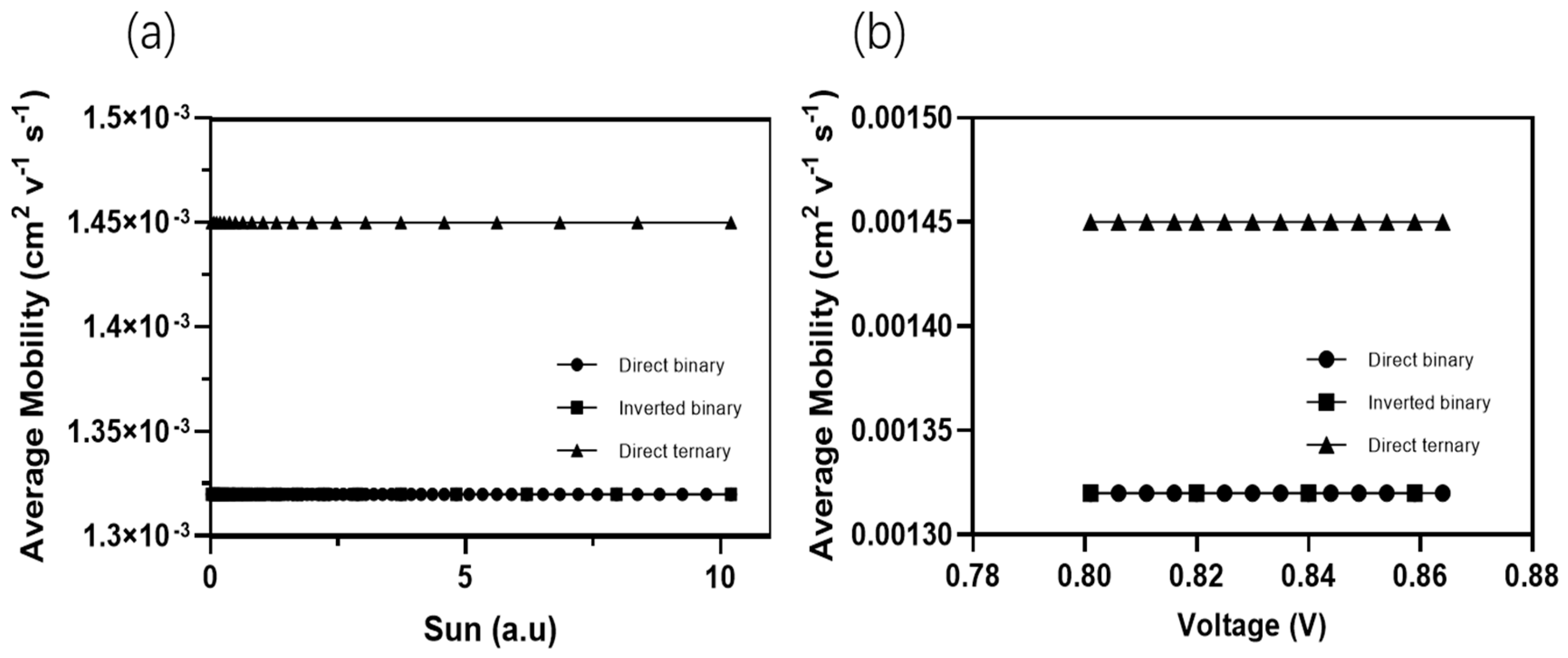
| Our work | ITO/PEDOT:PSS/PM6:L8-BO/SnO2/Ag | 0.859 | 26.5 | 80.4 | 18.34% |
| Our work | ITO/SnO2/PM6:L8-BO/PEDOT:PSS/Ag | 0.859 | 26.6 | 80.48 | 18.37% |
| Our work | FTO/PEDOT: PSS/PM6:D18:L8-BO/SnO2/Ag | 0.89 | 26.65 | 82.3 | 19.52% |
3. Results and Discussion
3.1. Device Performance
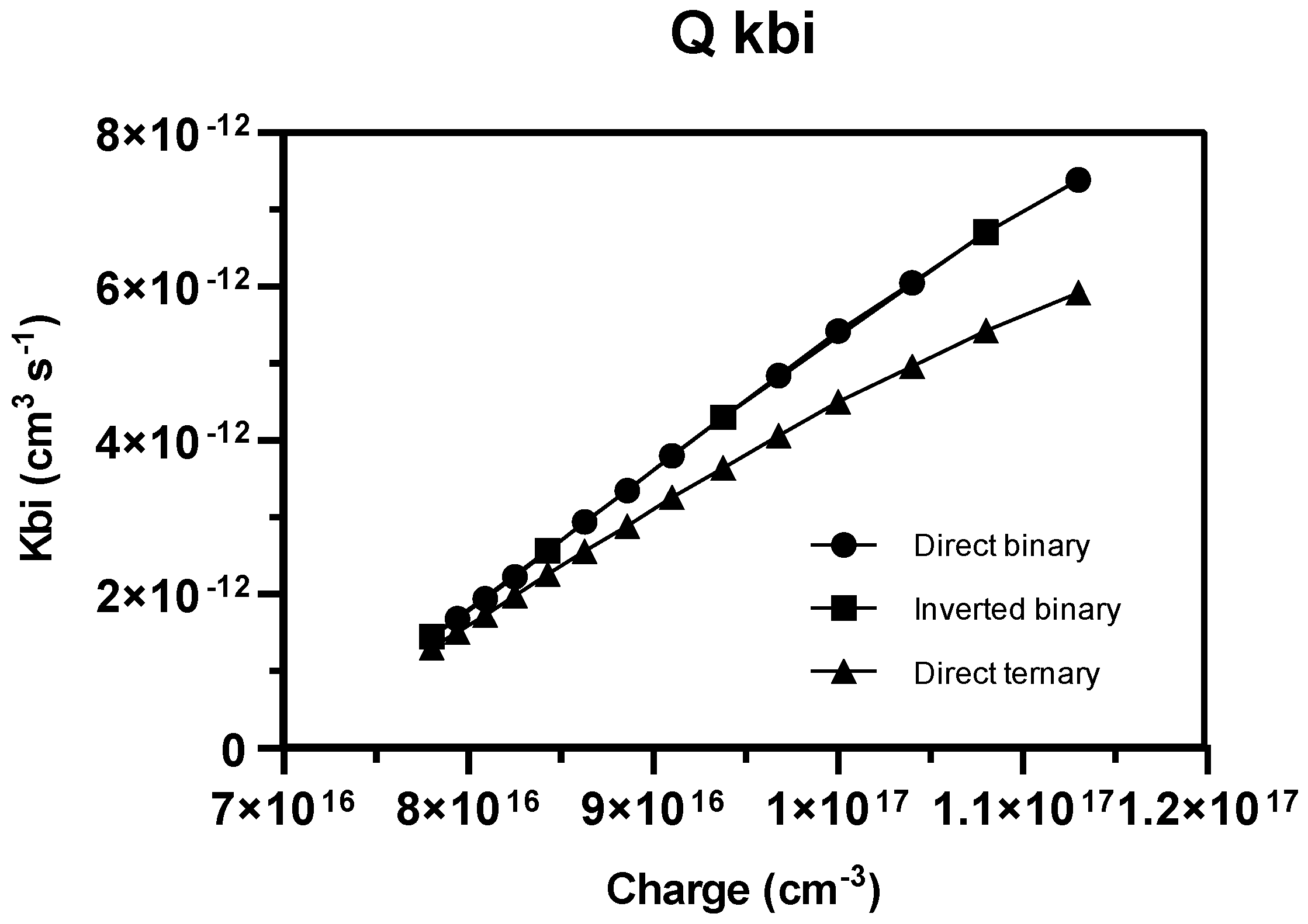
3.2. Charges Generation, Transport, and Recombination
4. Conclusions
Supplementary Materials
Author Contributions
Funding
Data Availability Statement
Conflicts of Interest
Nomenclature
| OSCs | Organic solar cells |
| PCE | Power conversion efficiency |
| NFAs | Non-fullerene acceptors |
| q | Elementary charge |
| SnO2 | Tin dioxide |
| ETL | Electron transport layer |
| HTL | Hole transport layer |
| BHJ | bulk heterojunction |
| HOMO | Highest occupied molecular orbital |
| LUMO | The lowest unoccupied molecular orbital |
| n | Density of free electrons |
| Nc,v | The effective density of states |
| Nt | The trap density of a single carrier trap |
| P | Density of free holes |
| Jn,p | The current flux density of the electron and holes |
| vth | The thermal emission velocity of the carriers |
| Ec,v | Conduction and valence bands |
| EF,h,e | The energy corresponding to fermi levels |
| Fn,p | The energy level of the Fermi level in the conduction and valence band |
| Dn,p | Diffusion coefficient |
| Rn | Recombination rate of electrons and holes |
| G | Carrier generation rate |
| KB | Boltzmann constant |
| T | Temperature |
| H | Magnetic field |
| Greek Symbols | |
| ε0 | Free permittivity |
| εr | Relative permittivity |
| φ | The voltage profile |
| µe,h | Electron and hole mobility |
| ΔE | Energy offset |
| бn,p | The trap cross-sections |
| ω | The angular frequency of the wave |
| λ | The speed of light |
| Superscript | |
| D | Electron donor |
| A | Electron Acceptor |
References
- Chen, L.X. Organic Solar Cells: Recent Progress and Challenges. ACS Energy Lett. 2019, 4, 2537–2539. [Google Scholar] [CrossRef]
- Burke, D.J.; Lipomi, D.J. Green chemistry for organic solar cells. Energy Environ. Sci. 2013, 6, 2053–2066. [Google Scholar] [CrossRef]
- Imamura, S.; Mizutani, T.; Kojima, K.; Ochiai, S. Characteristics and performance of organic photovoltaic cells having the active layer fabricated by ternary organic semiconducting materials. J. Photonics Energy 2011, 1, 011119. [Google Scholar] [CrossRef]
- Hong, L.; Yao, H.; Cui, Y.; Ge, Z.; Hou, J. Recent advances in high-efficiency organic solar cells fabricated by eco-compatible solvents at relatively large-area scale. APL Mater. 2020, 8, 120901. [Google Scholar] [CrossRef]
- Wang, X.; Sun, Q.; Gao, J.; Wang, J.; Xu, C.; Ma, X.; Zhang, F. Recent Progress of Organic Photovoltaics with Efficiency over 17%. Energies 2021, 14, 4200. [Google Scholar] [CrossRef]
- Farooq, W.; Khan, M.; Khan, A.D. High Performance Bulk-Heterojunction Organic Solar Cells. In Proceedings of the 2019 International Conference on Electrical, Communication, and Computer Engineering (ICECCE), Swat, Pakistan, 24–25 July 2019; pp. 1–6. [Google Scholar] [CrossRef]
- Putnin, T.; Lertvachirapaiboon, C.; Ishikawa, R.; Shinbo, K.; Kato, K.; Ekgasit, S.; Ounnunkad, K.; Baba, A. Enhanced organic solar cell performance: Multiple surface plasmon resonance and incorporation of silver nanodisks into a grating-structure electrode. Opto-Electron. Adv. 2019, 2, 1. [Google Scholar] [CrossRef]
- Würfel, P. Photovoltaic Principles and Organic Solar Cells. Chimia 2007, 61, 770. [Google Scholar] [CrossRef]
- Ghosekar, I.C.; Patil, G.C. Review on performance analysis of P3HT:PCBM-based bulk heterojunction organic solar cells. Semicond. Sci. Technol. 2021, 36, 045005. [Google Scholar] [CrossRef]
- Tadeson, G.; Sabat, R.G. Enhancement of the Power Conversion Efficiency of Organic Solar Cells by Surface Patterning of Azobenzene Thin Films. ACS Omega 2019, 4, 21862–21872. [Google Scholar] [CrossRef]
- Liang, S.; Xiao, C.; Xie, C.; Liu, B.; Fang, H.; Li, W. 13% Single-Component Organic Solar Cells based on Double-Cable Conjugated Polymers with Pendent Y-Series Acceptors. Adv. Mater. 2023, 35, e2300629. [Google Scholar] [CrossRef]
- Rhaman, M.M.; Matin, M.A. Organic Solar Cells: Historical developments and challenges. In Proceedings of the 2015 International Conference on Advances in Electrical Engineering (ICAEE), Dhaka, Bangladesh, 17–19 December 2015; pp. 26–29. [Google Scholar] [CrossRef]
- Fu, J.; Fong, P.W.; Liu, H.; Huang, C.S.; Lu, X.; Lu, S.; Abdelsamie, M.; Kodalle, T.; Sutter-Fella, C.M.; Yang, Y.; et al. 19.31% binary organic solar cell and low non-radiative recombination enabled by non-monotonic intermediate state transition. Nat. Commun. 2023, 14, 1760. [Google Scholar] [CrossRef] [PubMed]
- Zhu, L.; Zhang, M.; Xu, J.; Li, C.; Yan, J.; Zhou, G.; Zhong, W.; Hao, T.; Song, J.; Xue, X.; et al. Single-junction organic solar cells with over 19% efficiency enabled by a refined double-fibril network morphology. Nat. Mater. 2022, 21, 656–663. [Google Scholar] [CrossRef] [PubMed]
- Zhu, L.; Zhang, M.; Zhong, W.; Leng, S.; Zhou, G.; Zou, Y.; Su, X.; Ding, H.; Gu, P.; Liu, F.; et al. Progress and prospects of the morphology of non-fullerene acceptor based high-efficiency organic solar cells. Energy Environ. Sci. 2021, 14, 4341–4357. [Google Scholar] [CrossRef]
- Qi, F.; Jiang, K.; Lin, F.; Wu, Z.; Zhang, H.; Gao, W.; Li, Y.; Cai, Z.; Woo, H.Y.; Zhu, Z.; et al. Over 17% Efficiency Binary Organic Solar Cells with Photoresponses Reaching 1000 nm Enabled by Selenophene-Fused Nonfullerene Acceptors. ACS Energy Lett. 2021, 6, 9–15. [Google Scholar] [CrossRef]
- Lin, Y.; Firdaus, Y.; Nugraha, M.I.; Liu, F.; Karuthedath, S.; Emwas, A.H.; Zhang, W.; Seitkhan, A.; Neophytou, M.; Faber, H.; et al. 17.1% Efficient Single-Junction Organic Solar Cells Enabled by n-Type Doping of the Bulk-Heterojunction. Adv. Sci. 2020, 7, 1903419. [Google Scholar] [CrossRef] [PubMed]
- Li, C.; Zhou, J.; Song, J.; Xu, J.; Zhang, H.; Zhang, X.; Guo, J.; Zhu, L.; Wei, D.; Han, G.; et al. Non-fullerene acceptors with branched side chains and improved molecular packing to exceed 18% efficiency in organic solar cells. Nat. Energy 2021, 6, 605–613. [Google Scholar] [CrossRef]
- Greenstein, B.L.; Hutchison, G.R. Organic Photovoltaic Efficiency Predictor: Data-Driven Models for Non-Fullerene Acceptor Organic Solar Cells. J. Phys. Chem. Lett. 2022, 13, 4235–4243. [Google Scholar] [CrossRef]
- He, Q.; Kafourou, P.; Hu, X.; Heeney, M. Development of non-fullerene electron acceptors for efficient organic photovoltaics. SN Appl. Sci. 2022, 4, 247. [Google Scholar] [CrossRef]
- Wang, L.; An, Q.; Yan, L.; Bai, H.R.; Jiang, M.; Mahmood, A.; Yang, C.; Zhi, H.; Wang, J.L. Non-fullerene acceptors with hetero-dihalogenated terminals induce significant difference in single crystallography and enable binary organic solar cells with 17.5% efficiency. Energy Environ. Sci. 2022, 15, 320–333. [Google Scholar] [CrossRef]
- Gillett, A.J.; Privitera, A.; Dilmurat, R.; Karki, A.; Qian, D.; Pershin, A.; Londi, G.; Myers, W.K.; Lee, J.; Yuan, J.; et al. The role of charge recombination to triplet excitons in organic solar cells. Nature 2021, 597, 666–671. [Google Scholar] [CrossRef]
- Ioakeimidis, A.; Hauser, A.; Rossier, M.; Linardi, F.; Choulis, S.A. High-performance non-fullerene acceptor inverted organic photovoltaics incorporating solution processed doped metal oxide hole selective contact. Appl. Phys. Lett. 2022, 120, 233301. [Google Scholar] [CrossRef]
- Zhu, C.; Yuan, J.; Cai, F.; Meng, L.; Zhang, H.; Chen, H.; Li, J.; Qiu, B.; Peng, H.; Chen, S.; et al. Tuning the electron-deficient core of a non-fullerene acceptor to achieve over 17% efficiency in a single-junction organic solar cell. Energy Environ. Sci. 2020, 13, 2459–2466. [Google Scholar] [CrossRef]
- Li, J.; Zhang, Y.; Yuan, J.; Zhu, C.; Peng, H.; Zou, Y. Fine-tuning of non-fullerene acceptor gives over 14% efficiency for organic solar cells. Dye. Pigment. 2020, 181, 108559. [Google Scholar] [CrossRef]
- Zhang, Y.; Li, X.; Dai, T.; Xu, D.; Xi, J.; Chen, X. Charge transport and extraction of PTB7:PC71BM organic solar cells: Effect of film thickness and thermal-annealing. RSC Adv. 2019, 9, 24895–24903. [Google Scholar] [CrossRef] [PubMed]
- Xu, H.; Yuan, F.; Zhou, D.; Liao, X.; Chen, L.; Chen, Y. Hole transport layers for organic solar cells: Recent progress and prospects. J. Mater. Chem. A 2020, 8, 11478–11492. [Google Scholar] [CrossRef]
- Kong, T.; Yang, G.; Fan, P.; Yu, J. Solution-Processable NiOx:PMMA Hole Transport Layer for Efficient and Stable Inverted Organic Solar Cells. Polymers 2023, 15, 1875. [Google Scholar] [CrossRef] [PubMed]
- Yao, J.; Qiu, B.; Zhang, Z.G.; Xue, L.; Wang, R.; Zhang, C.; Chen, S.; Zhou, Q.; Sun, C.; Yang, C.; et al. Cathode engineering with perylene-diimide interlayer enabling over 17% efficiency single-junction organic solar cells. Nat. Commun. 2020, 11, 2726. [Google Scholar] [CrossRef]
- Jin, F.; Peng, R.; Qiu, Y.; Zhang, J.; Ge, Z. Highly Efficient and Stable Organic Solar Cells Enabled by a PEDOT:PSS/HxMoO3 Hybrid Hole Transport Layer. ACS Appl. Energy Mater. 2023, 6, 9532–9542. [Google Scholar] [CrossRef]
- Agnihotri, P.; Sahu, S.; Tiwari, S. Recent advances & perspectives in electron transport layer of organic solar cells for efficient solar energy harvesting. In Proceedings of the 2017 International Conference on Energy, Communication, Data Analytics and Soft Computing (ICECDS), Chennai, India, 1–2 August 2017; pp. 1568–1573. [Google Scholar] [CrossRef]
- Zhou, N.; Facchetti, A. Charge Transport and Recombination in Organic Solar Cells (OSCs). In Organic and Hybrid Solar Cells; Huang, H., Huang, J., Eds.; Springer International Publishing: Cham, Switzerland, 2014; pp. 19–52. [Google Scholar] [CrossRef]
- Yin, P.; Yin, Z.; Ma, Y.; Zheng, Q. Improving the charge transport of the ternary blend active layer for efficient semitransparent organic solar cells. Energy Environ. Sci. 2020, 13, 5177–5185. [Google Scholar] [CrossRef]
- Xu, Y.; Zhou, H.; Duan, P.; Shan, B.; Xu, W.; Wang, J.; Liu, M.; Zhang, F.; Sun, Q. Improving the Efficiency of Organic Solar Cells with Methionine as Electron Transport Layer. Molecules 2022, 27, 6363. [Google Scholar] [CrossRef] [PubMed]
- Bin, H.; Wang, J.; Li, J.; Wienk, M.M.; Janssen, R.A. Efficient Electron Transport Layer Free Small-Molecule Organic Solar Cells with Superior Device Stability. Adv. Mater. 2021, 33, 2008429. [Google Scholar] [CrossRef] [PubMed]
- Tara, A.; Bharti, V.; Sharma, S.; Gupta, R. Harnessing the Role of Charge Transport Layers for Efficient Design of PBDBT/ITIC-OE Based Organic Solar Cell. Trans. Electr. Electron. Mater. 2023, 24, 356–364. [Google Scholar] [CrossRef]
- Kong, T.; Wang, R.; Zheng, D.; Yu, J. Modification of the SnO2 Electron Transporting Layer by Using Perylene Diimide Derivative for Efficient Organic Solar Cells. Front. Chem. 2021, 9, 703561. [Google Scholar] [CrossRef] [PubMed]
- Niederhausen, J.; Mazzio, K.A.; MacQueen, R.W. Inorganic–organic interfaces in hybrid solar cells. Electron. Struct. 2021, 3, 033002. [Google Scholar] [CrossRef]
- Tang, H.; Bai, Y.; Zhao, H.; Qin, X.; Hu, Z.; Zhou, C.; Huang, F.; Cao, Y. Interface Engineering for Highly Efficient Organic Solar Cells. Adv. Mater. 2024, 36, 2212236. [Google Scholar] [CrossRef] [PubMed]
- Eliwi, A.A.; Byranvand, M.M.; Fassl, P.; Khan, M.R.; Hossain, I.M.; Frericks, M.; Ternes, S.; Abzieher, T.; Schwenzer, J.A.; Mayer, T.; et al. Optimization of SnO2 electron transport layer for efficient planar perovskite solar cells with very low hysteresis. Mater. Adv. 2022, 3, 456–466. [Google Scholar] [CrossRef]
- Di Mario, L.; Garcia Romero, D.; Wang, H.; Tekelenburg, E.K.; Meems, S.; Zaharia, T.; Portale, G.; Loi, M.A. Outstanding Fill Factor in Inverted Organic Solar Cells with SnO2 by Atomic Layer Deposition. Adv. Mater. 2024, 36, 2301404. [Google Scholar] [CrossRef] [PubMed]
- Schlachter, A.; Marineau-Plante, G.; Harvey, P.D.; Agrawal, A.; Sharma, G.D. Efficient ternary bulk heterojunction organic solar cells using a low-cost nonfullerene acceptor. J. Mater. Chem. C 2022, 10, 4372–4382. [Google Scholar] [CrossRef]
- Optoelectronic Simulation of an Organic Bulk Heterojunction Solar Cell with Comsol—Google Search. Available online: https://www.google.com.hk/imgres?q=optoelectronic%20simulation%20of%20an%20organic%20bulk%20heterojunction%20solar%20cell%20with%20comsol&imgurl=x-raw-image%3A%2F%2F%2F4262b3b8e6189a38d3a24a59663d11ff259ac5269379f3e6e15ab17ce487e3a9&imgrefurl=https%3A%2F%2Fwww.comsol.jp%2Fpaper%2Fdownload%2F187969%2FOptoelectronic-Simulation-of-An-Organic-Bulk-Heterojunction-Solar-Cell_Dr-Koh-Wee-Shing.pdf&docid=0xxlGyWoXRPPvM&tbnid=OJoY5rizYkL7jM&vet=1&w=1600&h=1131&hcb=2&itg=1&ved=2ahUKEwjwi4CsjemGAxU9cvUHHe7_D5gQM3oECBQQAA (accessed on 20 June 2024).
- MacKenzie, R.C.; Shuttle, C.G.; Dibb, G.F.; Treat, N.; von Hauff, E.; Robb, M.J.; Hawker, C.J.; Chabinyc, M.L.; Nelson, J. Interpreting the Density of States Extracted from Organic Solar Cells Using Transient Photocurrent Measurements. J. Phys. Chem. C 2013, 117, 12407–12414. [Google Scholar] [CrossRef]
- MacKenzie, R.C.I.; Shuttle, C.G.; Chabinyc, M.L.; Nelson, J. Extracting Microscopic Device Parameters from Transient Photocurrent Measurements of P3HT:PCBM Solar Cells. Adv. Energy Mater. 2012, 2, 662–669. [Google Scholar] [CrossRef]
- El Amine, B.M.; Zhou, Y.; Li, H.; Wang, Q.; Xi, J.; Zhao, C. Latest Updates of Single-Junction Organic Solar Cells up to 20% Efficiency. Energies 2023, 16, 3895. [Google Scholar] [CrossRef]
- Rafiq, M.; Haider, M.; Li, H.; Yang, J. Precise control of hole transport layer integration on PDTS-DTTFBT: PC71BM organic solar cells. Phys. Scr. 2024, 99, 055903. [Google Scholar] [CrossRef]
- Ram, K.S.; Singh, J. Over 20% Efficient and Stable Non-Fullerene-Based Ternary Bulk-Heterojunction Organic Solar Cell with WS2 Hole-Transport Layer and Graded Refractive Index Antireflection Coating. Adv. Theory Simul. 2020, 3, 2000047. [Google Scholar] [CrossRef]


| Devices | Voc (v) | Jsc (mA/cm2) | FF (%) | PCE (%) |
|---|---|---|---|---|
| S1: ITO/PEDOT:PSS/PM6:L8-BO/SnO2/Ag | 0.859 | 26.5 | 80.4 | 18.34% |
| S2: ITO/SnO2/PM6:L8-BO/PEDOT:PSS/Ag | 0.859 | 26.6 | 80.48 | 18.37% |
| S3: FTO/PEDOT:PSS/PM6:D18:L8-BO/SnO2/Ag | 0.89 | 26.65 | 82.3 | 19.52% |
Disclaimer/Publisher’s Note: The statements, opinions and data contained in all publications are solely those of the individual author(s) and contributor(s) and not of MDPI and/or the editor(s). MDPI and/or the editor(s) disclaim responsibility for any injury to people or property resulting from any ideas, methods, instructions or products referred to in the content. |
© 2024 by the authors. Licensee MDPI, Basel, Switzerland. This article is an open access article distributed under the terms and conditions of the Creative Commons Attribution (CC BY) license (https://creativecommons.org/licenses/by/4.0/).
Share and Cite
Boudia, M.E.A.; Wang, Q.; Zhao, C. Simulation and Comparison of the Photovoltaic Performance of Conventional and Inverted Organic Solar Cells with SnO2 as Electron Transport Layers. Energies 2024, 17, 3302. https://doi.org/10.3390/en17133302
Boudia MEA, Wang Q, Zhao C. Simulation and Comparison of the Photovoltaic Performance of Conventional and Inverted Organic Solar Cells with SnO2 as Electron Transport Layers. Energies. 2024; 17(13):3302. https://doi.org/10.3390/en17133302
Chicago/Turabian StyleBoudia, Mohamed El Amine, Qiuwang Wang, and Cunlu Zhao. 2024. "Simulation and Comparison of the Photovoltaic Performance of Conventional and Inverted Organic Solar Cells with SnO2 as Electron Transport Layers" Energies 17, no. 13: 3302. https://doi.org/10.3390/en17133302