Article

Simulation and Comparison of the Photovoltaic Performance of Conventional and Inverted Organic Solar Cells with SnO2 as Electron Transport Layers

MOE Key Laboratory of Thermo-Fluid Science and Engineering, School of Energy and Power Engineering, Xi’an Jiaotong University, Xi’an 710049, China
*
Author to whom correspondence should be addressed.
Energies 2024, 17(13), 3302; https://doi.org/10.3390/en17133302
Submission received: 4 June 2024 / Revised: 27 June 2024 / Accepted: 2 July 2024 / Published: 5 July 2024
(This article belongs to the Special Issue Organic and Hybrid Solar Cells for Efficient Solar Power Conversion)

Abstract

:
Extensive research on organic solar cells (OSCs) over the past decade has led to efficiency improvements exceeding 18%. Enhancing the efficacy of binary organic solar cells involves multiple factors, including the strategic selection of materials. The choice of donor and acceptor materials, which must exhibit complementary absorption spectra, is crucial. Additionally, optimizing the solar cell structure, such as adjusting the thickness of layers and incorporating hole-transporting layers, can further increase efficiency. In this study, we simulated three different novels within the use of the inorganic SnO2 on the OSCs within this specific arrangement of structures using a drift-diffusion model: direct and inverted binary; direct ternary configurations of OSCs, specifically ITO/PEDOT: PSS/PM6:L8-BO/SnO2/Ag, ITO/SnO2/PM6:L8-BO/PEDOT: PSS/Ag; and FTO/PEDOT: PSS/PM6:D18:L8-BO/SnO2/Ag. These structures achieved power conversion efficiencies (PCE) of 18.34%, 18.37%, and 19.52%, respectively. The direct ternary device achieved an important Voc of 0.89 V and an FF of 82.3%, which is high in comparison with other simulated results in the literature. Our research focused on the role of SnO2 as an inorganic electron transport layer in enhancing efficiency in all three configurations. We also evaluated the properties of these structures by simulating external quantum efficiency (EQE), which results in a broadened absorption spectrum from 380 nm to 900 nm for both binary and ternary devices. Furthermore, we measured the spectral distribution of absorbed photons, and photo-charge extraction by linearly increasing voltage (photo-CELIV) to assess charge extraction and generation rates as well as charge mobility. These measurements help establish a robust model for practical application.

1. Introduction

OSCs are known as a viable approach to efficiently capture sustainable and eco-friendly solar energy [1,2]. These materials possess a low weight exhibit flexibility, transparency, and high photon transmission, and are well-suited for industrial processes involving large-scale solution processing [3,4,5,6,7,8]. Nevertheless, some obstacles must be overcome before their widespread commercial use. Several problems exist in the field, including reduced PCE and a short lifetime [9,10,11,12]. The highest attainable PCE for binary and ternary OSCs is 19.3% and 19.2%, respectively [13,14]. The utilization of non-fullerene acceptors (NFAs) has been important in improving the PCE of OSCs [15,16,17]. The shape of the photoactive layer is considered a factor in achieving devices with outstanding efficiency [18,19,20,21]. To reduce loss channels and ensure that domain sizes are in line with excitons, carriers, and other photoelectron physical dynamics, it is crucial to manage the complex morphology of the photoactive layer [22,23,24,25]. The charge transport layers are of greatest significance in facilitating the transport of charges towards the electrodes [26,27]. The transport of charges within the active blend and the extraction of charges at the electrodes determines the overall efficiency of OSCs [28,29,30,31]. The incorporation of charge transport layers serves to boost the connection between the active surface and electrodes through the interfaces, hence developing the efficiencies of electron and hole extraction [32,33,34,35,36]. Tin dioxide (SnO2) exhibits favorable optoelectronic properties that make it an efficient material as an electron transport layer (ETL) in perovskite solar cells (PSCs) and OSCs [37,38]. These properties include suitable energy level alignment with the perovskite or organic active layers, high electron mobility, and processing under low temperatures [39]. Using an optimized SnO2 ETL can enhance surface passivation and increase energy loss between the ETL and either the perovskite or the organic active layer [40]. This, in turn, can reduce voltage losses and facilitate electron transfer [41]. The ternary bulk heterojunction (BHJ) architecture of OSCs is important in increasing the efficiency of OSCs [42]. The ternary BHJ architecture, by incorporating an additional component into the active layer, not only improves charge extraction but also enhances near-infrared absorption and reduces carrier recombination, contributing significantly to efficiency gains in OSCs [42].
Building on these insights and taking advantage of the previous literature that achieved a high PCE by Zhu et al. and Fu et al. [13,14], our study aims to simulate three different OSC configurations, direct binary, inverted binary, and direct ternary BHJ architectures, utilizing SnO2 as the ETL to enhance the efficiency of OSCs by using 1-dimensional optoelectronic software “Oghma-Nano 8.0.034” with a comprehensive simulation optical and electrical data input in the software referenced below in Section 2 and Section 3. We made a selection of different materials, and every material included its characteristics. We also made sure to construct original structures composed from those materials that had not been reported before as theoretical work to simulate new structures and discover their efficiency, which gave us an outline to make samples in the laboratory in the future. The simulated structures include ITO/PEDOT: PSS/PM6:L8-BO/SnO2/Ag, ITO/SnO2/PM6:L8-BO/PEDOT: PSS/Ag, and FTO/PEDOT: PSS/PM6:D18:L8-BO/SnO2/Ag. These configurations achieved PCEs of 18.34%, 18.37%, and 19.52%, respectively, demonstrating the effectiveness of SnO2 in improving solar cell performance.

2. Methods

2.1. Governing Equations

For general purposes, Oghma-Nano software was used to model the optical and electrical response of OSCs, which uses a finite difference approach to solve Maxwell domain’s frequency, the spectral absorbed energy density in the active layer, drift-diffusion equations, charge carrier continuity equations, and Poisson’s equation.
Maxwell’s domain’s frequency equation was used in the 1-dimensional optical model to calculate the distribution of photons. The electric and magnetic field is provided by Equations (1) and (2) [43].
H o p t x = j 2 π ν ɛ r ɛ 0 E o p t
and
E o p t x = j 2 π ν µ 0 H o p t
where H o p t represents the magnetic field vector, E o p t is the electric field vector, and ν is the frequency; ε0 and εr are the constants of free permittivity and the relative permittivity, respectively.
The spectral absorbed energy density in the active blend in 1-dimension at x position is as follows in Equation (3) [43]:
Q ν , x = 1 2 c ɛ 0 α η E o p t 2
and
α = 2 π k λ
where c is the speed of light, η is the refractive index, α is the absorption coefficient, k is the imaginary part of the refractive index, and λ is the incident light wavelength. The formation of excitons was dependent on the absorption of light photons, resulting in the production of a specific quantity as depicted in Equation (5) at each frequency and position [43]. All the optical inputs including η and α of the active layer, ETL, and HTL materials in Figures S15–S20 were used to calculate the distribution of the specter and the absorbed photon distribution, EQE, and IQE.
G ν , x = Q h ν = π ɛ r ɛ 0 h E o p t 2
where h is Planck’s constant. By resolving the continuity of charge carrier equations as specified in Equations (6) and (7), the conservation of the charge carriers is ensured [44].
J n x = q ( R n G + n t )
and
J p x = q ( R p G + p t )
where Rn and Rp are the recombination rate of electrons and holes, respectively, Jn and Jp are the electron and hole current density, respectively, q is the charge, n is the density of electrons, and p is the density of holes.
Maxwell–Boltzmann statistics are responsible for solving free carrier statistics as mentioned in Equations (8) and (9), which represent the solution of the equations of carrier densities of electrons and holes [45].
n = N c exp F n E c K B T
and
p = N v exp E v F p K B T
where Nc, Nv are the constants of the effective density of states in the conduction and valence band of a semiconductor, Fn,p are constants of the energy level of the Fermi level in the valence and conduction band, Ec is the conduction band, Ev is the valence band, KB is Boltzmann constant, and T is the temperature.
The solution of Poisson’s equation is used to obtain the distribution of potential within the device, and it is represented as follows in Equation (10) [44]:
  2 φ x 2 ɛ 0 ɛ r = q ( n p )
where φ is the electric potential. The transfer of charges is determined by solving the drift-diffusion equations that account for the movement of both electrons and holes as mentioned in Equations (11) and (12) below [45].
J n = q μ e n φ x + q D n n x
and
J p = q μ h p φ x + q D p p x
where Jn,p is the electron and hole current density, respectively, μe,h is the mobility of electrons and holes, respectively, and Dn,p is the electron and hole diffusion coefficient, respectively. The boundary conditions are represented as tunneling of electrons and holes through heterojunction interfaces provided by Equations (13) and (14).
J n = q T e ( n 1 n 1 e q n 0 n 0 e q )
and
J p = q T h ( p 1 p 1 e q p 0 p 0 e q )
where Te and Th are the rate constants of tunneling of electrons and holes, respectively, n0,1 is the number of electrons in the layers before and after the interface, p0,1 is the number of holes in the layers before and after the interface, n 0,1 e q is the equilibrium number of electrons in the layers before and after the interface, and p 0,1 e q is the equilibrium number of holes in the layers before and after the interface.
A full description of the electrical and optical model [45] of our simulation is shown in Table 1 and Table 2.

2.2. Evaluation of the Performance Indicators

The objective of our study was to improve the PCE of OSCs, which is represented by Equation (15) [46].
P C E = P m a x I i n = J s c V o c F F I i n
where Pmax is the maximum power output by the OSC, and Iin is the illumination intensity. The Voc value represents the highest voltage when the current is null through the device, and it is represented as follows:
V o c = E g Δ E q
and
Δ E = 2 E F , h E H O M O D K B T   l n µ e   µ h
where Δ E is the energy offset, the, FF presents the maximum power output of the OSCs, which is defined below the Equation (18) [46].
F F = P m a x V o c J s c = V m V o c 1 e q A k T ( V m V o c )
where A is the ideality factor of the semi-conductor.
Table 2. Comparison between our direct and inverted binary OSCs and TOSCs with other simulation studies.
ReferenceStructureVoc (v)Jsc (mA/cm2)FF (%)PCE (%)
Rafiq et al. [47]ITO/MoO3/PDTS-DTTFBT:PC71BM/C60/PC60BM/ZnO/Ag0.99920.0188.5217.69%
Ram et al. [48]ITO/WS2/PBDB-T-2F:Y6:PC71BM/PFN-Br/Al0.8525.18017.10%
Zhu et al. [14]ITO/PEDOT:PSS/PM6:D18:L8-BO/PNDIT-F3N/Ag0.8724.4980.3817.21%
Our workITO/PEDOT:PSS/PM6:L8-BO/SnO2/Ag0.85926.580.418.34%
Our workITO/SnO2/PM6:L8-BO/PEDOT:PSS/Ag0.85926.680.4818.37%
Our workFTO/PEDOT: PSS/PM6:D18:L8-BO/SnO2/Ag0.8926.6582.319.52%

3. Results and Discussion

3.1. Device Performance

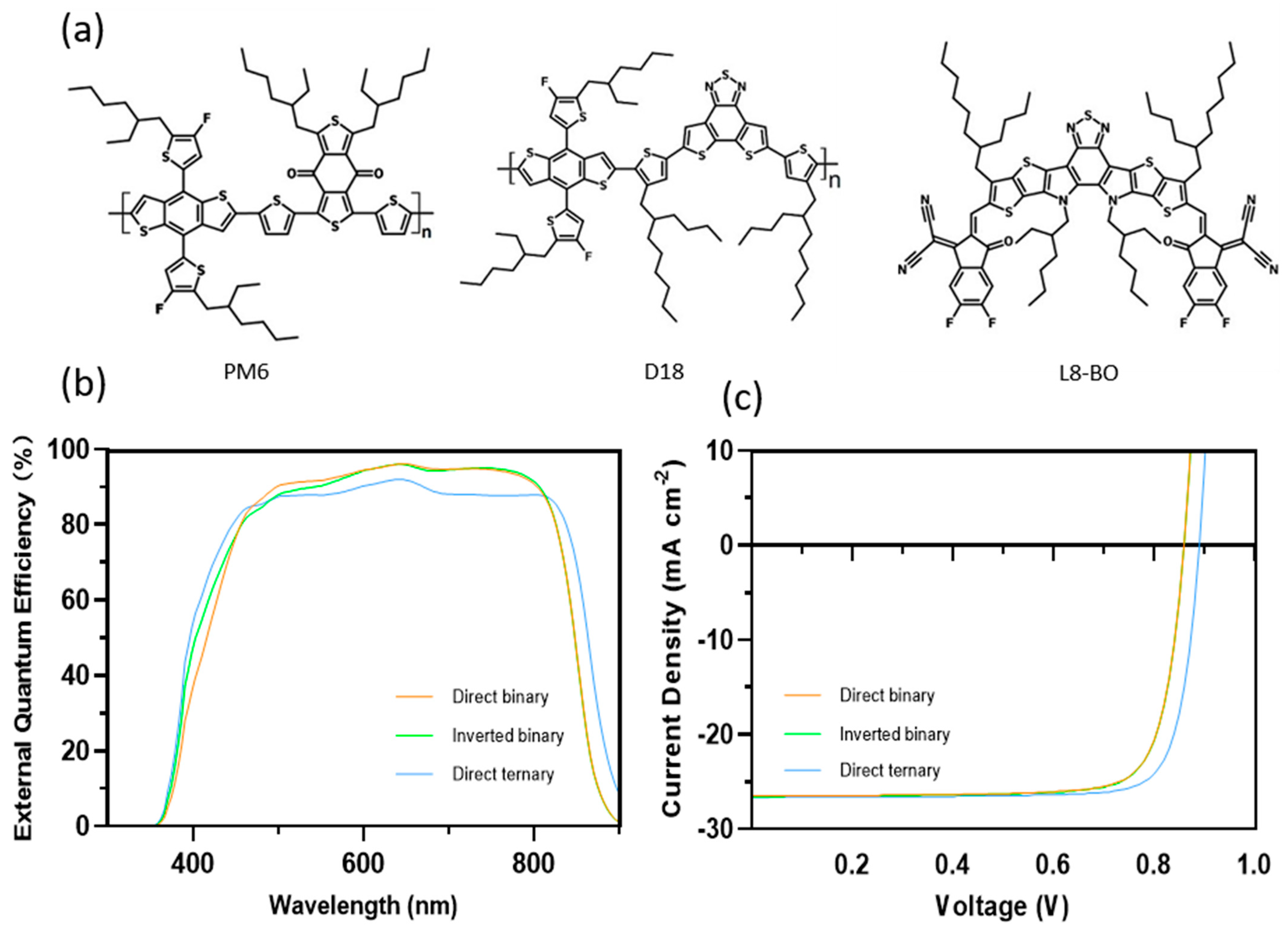
Figure 1a,b and Figure 2 represent the 1-dimensional device structures of the inverted binary, direct binary, and direct ternary, respectively. Figure 3a depicts the chemical material architecture and the absorption wavelength of the materials used in this work. They are protons that are predominantly absorbed between 550 and 900 nm [14].
PM6 and D18 serve as means to capture photons with short wavelengths from 400 to 700 nm [14]. Furthermore, the utilization of this particular combination enables the manipulation of material crystallization processes, leading to the creation of a donor phase that exhibits exceptional crystalline characteristics [14].
The J-V characteristics were simulated under AM 1.5 G illumination with an intensity of 100 mW cm−2. The findings are presented in Figure 3c and Table 2. The three devices direct binary, inverted binary, and direct ternary structures (see Figure 1a,b and Figure 2) achieved 18.34%, 18.37%, and 19.52%, respectively. Additionally, the devices result in Jsc of 26.5 mA cm−2, 26.6 mA cm−2, and 26.65 mA cm−2, respectively. For the Voc, they exhibit 0.859 V, 0.859 V, and 0.89 V, respectively. The FF exhibits 80.4%, 80.48%, and 82.3%, respectively. Both conventional and inverted binary structures showed the same improved PCE of approximately 18.3% since we used SnO2 as an ETL. The ternary device resulted in the best efficiency performance of 19.52%, while the FF and Voc increased from 80.4% to 82.3% and from 0.859 V to 0.89 V, respectively. The high value of the FF for TOSCs is related to the optimization of the active layer of the solar cell that requires it to have a bi-continuous shape with suitable and solidified nanoscale domains. Efficient charge transport and reduced recombination are dependent on this.
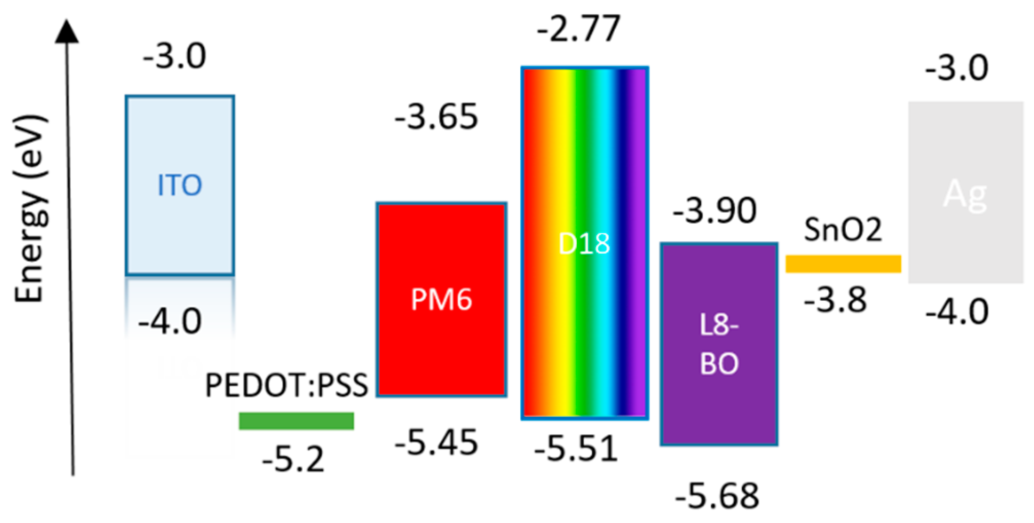
In addition, the widened absorption spectra by the insertion of a third component can broaden the absorption spectra, which enhances light harvesting and raises the short-circuit current. Furthermore, the third component can assist in suppressing the morphological evolution of the host mix, resulting in better stability, and serves as a bridging unit to systematically optimize charge migration, exciton lifespan, recombination, and nanomorphology. The development of the ternary devices was marked by the addition of D18 as a third element and a 2nd donor to the structure, which created more cascaded energy levels for the devices, according to Figure 4, Figures S3 and S4, and facilitates the electron transport toward the electrodes. The Jsc has slightly improved the binary devices to 26.65 mA cm−2 due to the slight enhancement in the absorption specter by adding the third element, which results in more exciton creation.

3.2. Charges Generation, Transport, and Recombination

The EQE and IQE of the three OSCs are shown in Figure 3b and Figure S1. EQE quantifies the efficiency of a solar cell in converting light energy into electrical energy. The term “quantum efficiency” refers to the ratio of the number of carriers gathered by the solar cell to the number of photons with a specific energy that hit the solar cell. The quantum efficiency at a specific wavelength is unified when all photons of that wavelength are absorbed and the ensuing minority carriers are collected. Photons with energy below the band gap have a quantum efficiency of zero. The integrated current in a solar cell is directly linked to the EQE. By integrating the quantum efficiency of the cell across the entire solar electromagnetic spectrum, it is possible to determine the current that the cell will generate when exposed to sunlight. The results of the integrated current are depicted in Figures S21–S23 for direct, inverted binary, and direct ternary, respectively. EQE(λ) is directly proportional to the current divided by the photon flux. The results indicate an absorption spectrum from 380 nm to 870 nm for both binary devices and a wide absorption from 380 nm to 900 nm for ternary devices. A notable disparity in absorption wavelengths is observed between ternary and binary devices. Specifically, within the range of 510 nm to 820 nm, binary devices exhibit a higher absorption rate. This is evidenced by peak values of 95% at 650 nm and 94% at 770 nm for both direct and inverted binary devices. In contrast, the ternary device demonstrates a slightly lower absorption rate, with a peak value of 90% at 650 nm. Furthermore, the average absorption within the same range for ternary devices is 85%, which is less than that of binary devices. The ternary device presents a wide range of EQE due to the incorporation of a third material. This additional material contributes to the broadening of the absorption wavelength and the generation of more excitons. In contrast, binary devices show slightly higher absorption from 510 nm to 820 nm. This is attributed to the redistribution of absorbed photons across two band gaps in the organic materials, which allows for the absorption of a larger quantity of photons within this specific range. The inclusion of a third material in the ternary active blend resulted in enhanced photon absorption within the visible wavelength range, as well as widened absorption wavelengths to encompass the near-infrared range (NIR) spectrum. This modification led to an improvement in the Jsc. In Figure 4, Figures S3 and S4, we observed that PM6 exhibits a home energy of −5.20 eV and a LUMO energy of −3.06 eV. The energy levels for D18 are −5.24 eV and −2.95 eV, while for L8-BO, they are −5.67 eV and −3.92 eV, respectively. Equation (19), which represents the energy offset (ΔE), is a crucial parameter that influences the performance of charge transportation. If the magnitude of ΔE is equal to or higher than the exciton binding energy (EB), there is a possibility that the vibrational energy of the released molecule could drive the dissociation of excitons [48].
Δ E = E D H O M O E A H O M O
The ternary strategy makes more straightforward pathways for charges to reach the electrodes because it minimizes the ΔE between the active blend and the charge transport layers. This is strong evidence of the Voc and the FF improvement for the ternary OSC compared to binary devices, as we witnessed in the previous performance in Figure 3 and Table 2.
An optical simulation was performed to the device’s efficiency of light absorption and exciton generation. Figure 5, Figure 6, and Figures S8–S11 display the wavelength distributions of incident photons and absorbed photons for direct binary, inverted, and direct ternary devices, respectively. The active blends in the three devices showed great absorption within the wavelength between 510 nm and 810 nm, while the ternary device had slightly broader absorption than the other devices from 370 nm to 880 nm, as evidenced by the EQE previously.
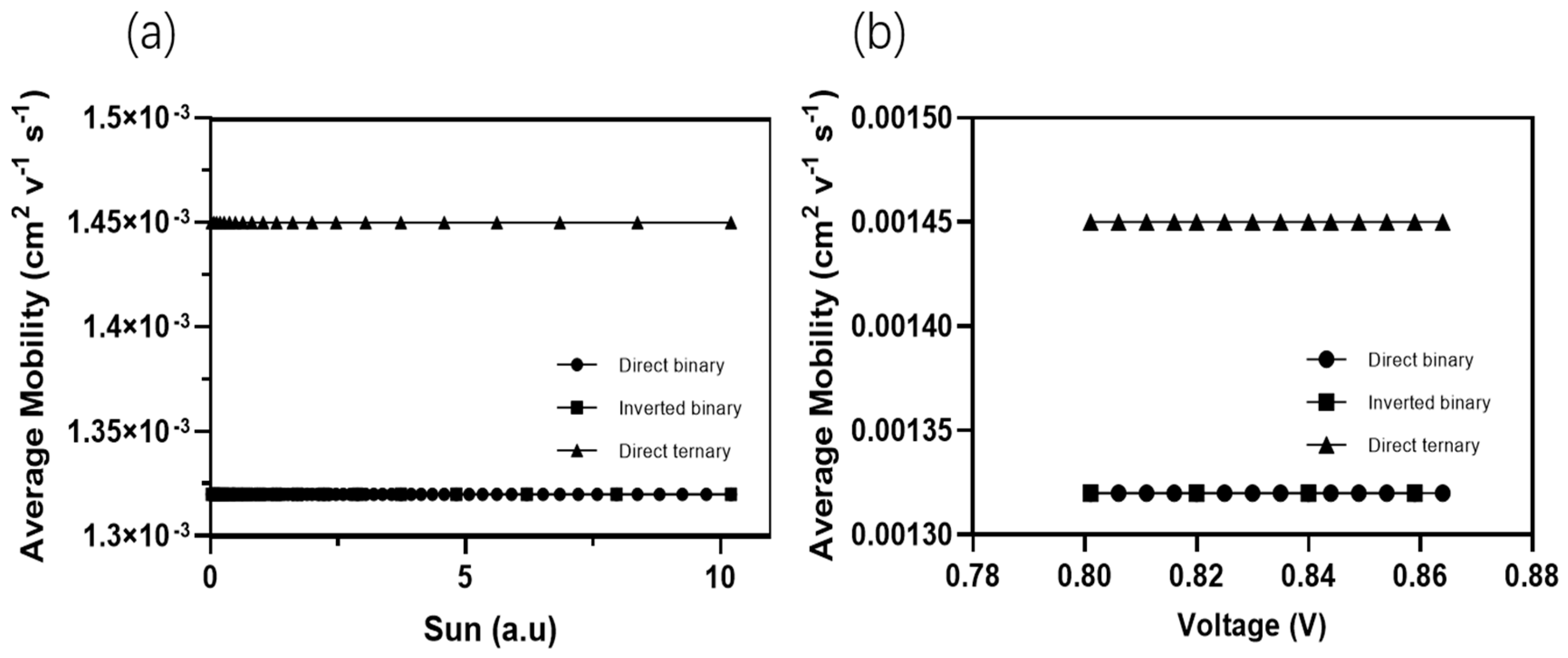
The mobility of charge greatly influences the efficiency of OSCs. Figure 7a,b depicts the average charge mobilities in the function of illumination and voltage. The ternary device showed the best average mobility of 1.45 × 10⁻³ cm2 V−1 s−1 than both binary direct and inverted devices within an approximately equal value of 1.32 × 10⁻³ cm2 V−1 s−1. As a result of the high mobility of ternary structure, the Voc improved to 0.89 V due to the reduction of energy losses on the interfaces between the charge transport layers and active layer based on Equations (16) and (17), which demonstrates the importance of increasing the mobility of the charge to minimize the energy loss to increase the charge transport and obtain a high Voc. On the other hand, the charge recombination was primarily responsible for determining the incidence of Voc loss. The phenomenon of charge recombination is dependent on the carrier’s mobility.
The measurement of charge extraction is conducted using the photo-CELIV and is shown in the supporting information (Figures S11–S13). For both binary (direct and inverted structures) and ternary devices with the following mobilities of 1.45 × 10⁻³ cm2 V−1 s−1 and 1.32 × 10⁻³ cm2 V−1 s−1, respectively. The devices show a close transient charge extraction and generation rate of charge carriers (see Figures S5–S7). This can be described by the close Jsc result for the three structures of direct binary, inverted binary, and direct ternary of 26.5 mA cm−2, 26.6 mA cm−2, and 26.65 mA cm−2, respectively.
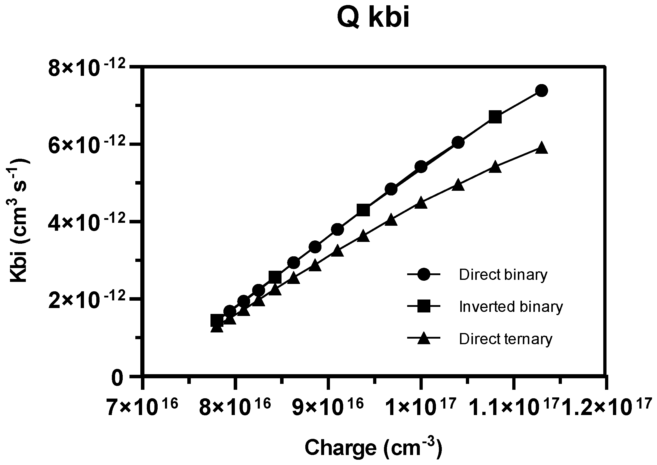
The recombination prefactor (Kbi) was subjected to the effect of multiple factors, such as the mobility of carriers, the electric field, and the density of states [32]. The utilization of the Kbi has been employed as a modeling parameter to characterize the Voc and FF of OSCs [32]. Figure 8 shows the Kbi measurement of the different devices, such as conventional binary, inverted binary, and ternary.
The binary devices showed slightly the same recombination rate value of the average 5 × 10⁻¹² cm3 s−1, while the ternary device showed a decreased value of 3 × 10⁻¹² cm3 s−1. The low recombination rate observed in ternary devices facilitates efficient charge extraction and transport within the anode and cathode paths, as mediated by the distinct charge transport layers. Moreover, the Voc and FF outcomes of this particular device exhibit significant improvements when compared to binary devices.
We compared other theoretical studies represented in Table 2 conducted by Rafiq et al. [47], Ram et al. [48], and Zhu et al. [14] with our findings by simulation of inverted and direct binary and direct ternary OSCs. Our simulated structures demonstrated significant advancements in the PCE of single-junction OSCs, surpassing the results of previous studies reported in Table 2. Furthermore, we noticed a great achievement in Jsc of 26.5 mA cm−2, 26.6 mA cm−2, and 26.65 mA cm−2 for direct, inverted binary, and ternary OSCs, respectively, compared with other simulated results in the table because of the broadened absorption wavelength of EQE depicted by this structure. Also, the optimization thickness of the active layer at 80 nm played a key role in facilitating the exciton separation and the creation of free charge carriers, which contributed to enhancing the Jsc. In addition, our ternary device achieved a higher Voc result of 82.3 V than Ram et al. and Zhu et al. However, the study of Rafiq et al. achieved a slightly higher Voc and FF than our TOSC devices within the values 0.999 V and 88.52%, respectively. By analyzing their structure, we found that the key point in their achievement of Voc and FF was in the use of triple ETL of C60, PC60BM, and ZnO, which created a close energy alignment between the LUMO of these materials and a cascaded energy level that facilitated electron transfer toward the Ag electrode. On the other hand, despite their important achievement of Voc and FF, our TOSCs achieved a higher PCE of 19.52%, which is higher than their study, and the PCE is supposed to be the important parameter to consider and was the ultimate goal of this research.

4. Conclusions

We investigated the effectiveness of the inorganic ETL SnO2 by performing three distinct structures: direct, inverted binary, and direct ternary structures within the structures ITO/PEDOT: PSS/PM6:L8-BO/SnO2/Ag, ITO/SnO2/PM6:L8-BO/PEDOT: PSS/Ag, and FTO/PEDOT: PSS/PM6:D18:L8-BO/SnO2/Ag, respectively. These structures achieved power conversion efficiencies of 18.34%, 18.37%, and 19.52%, respectively. Further, the integration of SnO2 not only established a series of interconnected energy levels between the active layer and both electrodes but also improved the transit of electrons. This contribution played a vital role in enhancing the Voc of the devices. The Voc values were measured at 0.859 V, 0.86 V, and 0.89 V for the conventional binary, inverted binary, and direct ternary devices, respectively. In addition, we optimized the thickness of the active layer for the three devices at 80 nm to enhance the efficiency of the exciton diffusion length, which achieved an average Jsc value of 26.6 mA cm−2, which is higher than the compared literature’s results. At the same time, we obtained a broadened absorption spectrum from 380 nm to 900 nm for both binary and ternary devices by EQE measurements. The main objective of future research efforts should be to employ a global strategy to optimize the overall configuration of OSCs. This involves examining different factors, such as employing optical engineering methods to improve light absorption and reduce reflection, studying the physical properties of the cells through electronic and mathematical analyses to determine important variables, and researching new materials and microscopic structures to create more efficient materials. The primary objective is to optimize the efficiency of OSCs. These developments have a substantial influence on the overall enhancement of the device’s efficiency.

Supplementary Materials

The following supporting information can be downloaded at: https://www.mdpi.com/article/10.3390/en17133302/s1, Figure S1: Internal quantum efficiency (IQE) of the conventional and inverted binary, and ternary devices; Figure S2: The reflected light as a function of the wavelength for conventional and inverted binary, and ternary devices; Figure S3: Energy levels diagram for Conventional binary organic solar cells; Figure S4: Energy levels diagram for Inverted binary organic solar cells; Figure S5: Charge carrier generation rate with energy level alignment of different materials of the conventional binary device in function of position; Figure S6: Charge carrier generation rate with energy level alignment of different materials of the Imverted binary device in function of position; Figure S7: Charge carrier generation rate with energy level alignment of different materials of the Ternary device in function of position; Figure S8: The distribution of the specterspecter of incident photons of the D-A active layer PM6:D18:L8-BO for conventional binary devices; Figure S9: The distribution of the specter of the absorbed photons of the D-A active layer PM6:L8-BO for inverted binary device; Figure S10: The distribution of the specter of the absorbed photons of the D-A active layer PM6:L8-BO for inverted binary device; Figure S11: The distribution of the specterspecter of the absorbed photons of the D-A blend PM6:L8-BO for the Ternary device; Figure S12: (a) transient current density for conventional binary devices; (b) transient current for for conventional binary devices; (c) transient generation rate for conventional binary devices; and (d) transient voltage for conventional binary devices; Figure S13: (a) transient current density for inverted binary devices; (b) transient current for the different mobilities for inverted binary devices; (c) transient generation rate for inverted binary devices; and (d) transient voltage for inverted binary devices; Figure S14: (a) transient current density for ternary; (b) transient current ternary devices; (c) transient generation rate for all devices; and (d) transient voltage for ternary devices; Figure S15: The absorption of light of the active layers PM6:L8-BO and PM6:D18:L8-BO; Figure S16: The refractive index of the active layers PM6:L8-BO and PM6:D18:L8-BO; Figure S17: The absorption of light of PEDOT: PSS.; Figure S18: The refractive index of PEDOT: PSS.; Figure S19: The absorption of light of SnO2; Figure S20: The refractive index of SnO2; Figure S21: EQE and the integrated Jsc curve of the direct binary device; Figure S22: EQE and the integrated Jsc curve of the inverted binary device; Figure S23: EQE and the integrated Jsc curve of the direct ternary device; Table S1: The thicknesses of the different layers of the conventional, inverted structure of binary, and ternary organic solar cells for optimum efficiency; Table S2: Simulation parameters of Oghma-Nano software for the binary conventional, and inverted PM6:L8-BO structures, and ternary devices.

Author Contributions

Conceptualization, M.E.A.B.; Methodology, M.E.A.B.; Software, M.E.A.B.; Formal analysis, M.E.A.B.; Writing—original draft, M.E.A.B.; Writing—review & editing, Q.W. and C.Z.; Visualization, M.E.A.B.; Supervision, C.Z.; Project administration, M.E.A.B.; Funding acquisition, C.Z. All authors have read and agreed to the published version of the manuscript.

Funding

This work was supported by the National Natural Science Foundation of China (No. 51976157) and the Fundamental Research Funds for the Central Universities.

Data Availability Statement

The data are available upon reasonable request from the corresponding author.

Conflicts of Interest

The authors declare no conflicts of interest.

Nomenclature

OSCsOrganic solar cells
PCEPower conversion efficiency
NFAsNon-fullerene acceptors
qElementary charge
SnO2Tin dioxide
ETLElectron transport layer
HTLHole transport layer
BHJbulk heterojunction
HOMOHighest occupied molecular orbital
LUMOThe lowest unoccupied molecular orbital
nDensity of free electrons
Nc,vThe effective density of states
NtThe trap density of a single carrier trap
PDensity of free holes
Jn,pThe current flux density of the electron and holes
vthThe thermal emission velocity of the carriers
Ec,vConduction and valence bands
EF,h,eThe energy corresponding to fermi levels
Fn,pThe energy level of the Fermi level in the conduction and valence band
Dn,pDiffusion coefficient
RnRecombination rate of electrons and holes
GCarrier generation rate
KBBoltzmann constant
TTemperature
HMagnetic field
Greek Symbols
ε0Free permittivity
εrRelative permittivity
φThe voltage profile
µe,hElectron and hole mobility
ΔEEnergy offset
бn,pThe trap cross-sections
ωThe angular frequency of the wave
λThe speed of light
Superscript
DElectron donor
AElectron Acceptor

References

  1. Chen, L.X. Organic Solar Cells: Recent Progress and Challenges. ACS Energy Lett. 2019, 4, 2537–2539. [Google Scholar] [CrossRef]
  2. Burke, D.J.; Lipomi, D.J. Green chemistry for organic solar cells. Energy Environ. Sci. 2013, 6, 2053–2066. [Google Scholar] [CrossRef]
  3. Imamura, S.; Mizutani, T.; Kojima, K.; Ochiai, S. Characteristics and performance of organic photovoltaic cells having the active layer fabricated by ternary organic semiconducting materials. J. Photonics Energy 2011, 1, 011119. [Google Scholar] [CrossRef]
  4. Hong, L.; Yao, H.; Cui, Y.; Ge, Z.; Hou, J. Recent advances in high-efficiency organic solar cells fabricated by eco-compatible solvents at relatively large-area scale. APL Mater. 2020, 8, 120901. [Google Scholar] [CrossRef]
  5. Wang, X.; Sun, Q.; Gao, J.; Wang, J.; Xu, C.; Ma, X.; Zhang, F. Recent Progress of Organic Photovoltaics with Efficiency over 17%. Energies 2021, 14, 4200. [Google Scholar] [CrossRef]
  6. Farooq, W.; Khan, M.; Khan, A.D. High Performance Bulk-Heterojunction Organic Solar Cells. In Proceedings of the 2019 International Conference on Electrical, Communication, and Computer Engineering (ICECCE), Swat, Pakistan, 24–25 July 2019; pp. 1–6. [Google Scholar] [CrossRef]
  7. Putnin, T.; Lertvachirapaiboon, C.; Ishikawa, R.; Shinbo, K.; Kato, K.; Ekgasit, S.; Ounnunkad, K.; Baba, A. Enhanced organic solar cell performance: Multiple surface plasmon resonance and incorporation of silver nanodisks into a grating-structure electrode. Opto-Electron. Adv. 2019, 2, 1. [Google Scholar] [CrossRef]
  8. Würfel, P. Photovoltaic Principles and Organic Solar Cells. Chimia 2007, 61, 770. [Google Scholar] [CrossRef]
  9. Ghosekar, I.C.; Patil, G.C. Review on performance analysis of P3HT:PCBM-based bulk heterojunction organic solar cells. Semicond. Sci. Technol. 2021, 36, 045005. [Google Scholar] [CrossRef]
  10. Tadeson, G.; Sabat, R.G. Enhancement of the Power Conversion Efficiency of Organic Solar Cells by Surface Patterning of Azobenzene Thin Films. ACS Omega 2019, 4, 21862–21872. [Google Scholar] [CrossRef]
  11. Liang, S.; Xiao, C.; Xie, C.; Liu, B.; Fang, H.; Li, W. 13% Single-Component Organic Solar Cells based on Double-Cable Conjugated Polymers with Pendent Y-Series Acceptors. Adv. Mater. 2023, 35, e2300629. [Google Scholar] [CrossRef]
  12. Rhaman, M.M.; Matin, M.A. Organic Solar Cells: Historical developments and challenges. In Proceedings of the 2015 International Conference on Advances in Electrical Engineering (ICAEE), Dhaka, Bangladesh, 17–19 December 2015; pp. 26–29. [Google Scholar] [CrossRef]
  13. Fu, J.; Fong, P.W.; Liu, H.; Huang, C.S.; Lu, X.; Lu, S.; Abdelsamie, M.; Kodalle, T.; Sutter-Fella, C.M.; Yang, Y.; et al. 19.31% binary organic solar cell and low non-radiative recombination enabled by non-monotonic intermediate state transition. Nat. Commun. 2023, 14, 1760. [Google Scholar] [CrossRef] [PubMed]
  14. Zhu, L.; Zhang, M.; Xu, J.; Li, C.; Yan, J.; Zhou, G.; Zhong, W.; Hao, T.; Song, J.; Xue, X.; et al. Single-junction organic solar cells with over 19% efficiency enabled by a refined double-fibril network morphology. Nat. Mater. 2022, 21, 656–663. [Google Scholar] [CrossRef] [PubMed]
  15. Zhu, L.; Zhang, M.; Zhong, W.; Leng, S.; Zhou, G.; Zou, Y.; Su, X.; Ding, H.; Gu, P.; Liu, F.; et al. Progress and prospects of the morphology of non-fullerene acceptor based high-efficiency organic solar cells. Energy Environ. Sci. 2021, 14, 4341–4357. [Google Scholar] [CrossRef]
  16. Qi, F.; Jiang, K.; Lin, F.; Wu, Z.; Zhang, H.; Gao, W.; Li, Y.; Cai, Z.; Woo, H.Y.; Zhu, Z.; et al. Over 17% Efficiency Binary Organic Solar Cells with Photoresponses Reaching 1000 nm Enabled by Selenophene-Fused Nonfullerene Acceptors. ACS Energy Lett. 2021, 6, 9–15. [Google Scholar] [CrossRef]
  17. Lin, Y.; Firdaus, Y.; Nugraha, M.I.; Liu, F.; Karuthedath, S.; Emwas, A.H.; Zhang, W.; Seitkhan, A.; Neophytou, M.; Faber, H.; et al. 17.1% Efficient Single-Junction Organic Solar Cells Enabled by n-Type Doping of the Bulk-Heterojunction. Adv. Sci. 2020, 7, 1903419. [Google Scholar] [CrossRef] [PubMed]
  18. Li, C.; Zhou, J.; Song, J.; Xu, J.; Zhang, H.; Zhang, X.; Guo, J.; Zhu, L.; Wei, D.; Han, G.; et al. Non-fullerene acceptors with branched side chains and improved molecular packing to exceed 18% efficiency in organic solar cells. Nat. Energy 2021, 6, 605–613. [Google Scholar] [CrossRef]
  19. Greenstein, B.L.; Hutchison, G.R. Organic Photovoltaic Efficiency Predictor: Data-Driven Models for Non-Fullerene Acceptor Organic Solar Cells. J. Phys. Chem. Lett. 2022, 13, 4235–4243. [Google Scholar] [CrossRef]
  20. He, Q.; Kafourou, P.; Hu, X.; Heeney, M. Development of non-fullerene electron acceptors for efficient organic photovoltaics. SN Appl. Sci. 2022, 4, 247. [Google Scholar] [CrossRef]
  21. Wang, L.; An, Q.; Yan, L.; Bai, H.R.; Jiang, M.; Mahmood, A.; Yang, C.; Zhi, H.; Wang, J.L. Non-fullerene acceptors with hetero-dihalogenated terminals induce significant difference in single crystallography and enable binary organic solar cells with 17.5% efficiency. Energy Environ. Sci. 2022, 15, 320–333. [Google Scholar] [CrossRef]
  22. Gillett, A.J.; Privitera, A.; Dilmurat, R.; Karki, A.; Qian, D.; Pershin, A.; Londi, G.; Myers, W.K.; Lee, J.; Yuan, J.; et al. The role of charge recombination to triplet excitons in organic solar cells. Nature 2021, 597, 666–671. [Google Scholar] [CrossRef]
  23. Ioakeimidis, A.; Hauser, A.; Rossier, M.; Linardi, F.; Choulis, S.A. High-performance non-fullerene acceptor inverted organic photovoltaics incorporating solution processed doped metal oxide hole selective contact. Appl. Phys. Lett. 2022, 120, 233301. [Google Scholar] [CrossRef]
  24. Zhu, C.; Yuan, J.; Cai, F.; Meng, L.; Zhang, H.; Chen, H.; Li, J.; Qiu, B.; Peng, H.; Chen, S.; et al. Tuning the electron-deficient core of a non-fullerene acceptor to achieve over 17% efficiency in a single-junction organic solar cell. Energy Environ. Sci. 2020, 13, 2459–2466. [Google Scholar] [CrossRef]
  25. Li, J.; Zhang, Y.; Yuan, J.; Zhu, C.; Peng, H.; Zou, Y. Fine-tuning of non-fullerene acceptor gives over 14% efficiency for organic solar cells. Dye. Pigment. 2020, 181, 108559. [Google Scholar] [CrossRef]
  26. Zhang, Y.; Li, X.; Dai, T.; Xu, D.; Xi, J.; Chen, X. Charge transport and extraction of PTB7:PC71BM organic solar cells: Effect of film thickness and thermal-annealing. RSC Adv. 2019, 9, 24895–24903. [Google Scholar] [CrossRef] [PubMed]
  27. Xu, H.; Yuan, F.; Zhou, D.; Liao, X.; Chen, L.; Chen, Y. Hole transport layers for organic solar cells: Recent progress and prospects. J. Mater. Chem. A 2020, 8, 11478–11492. [Google Scholar] [CrossRef]
  28. Kong, T.; Yang, G.; Fan, P.; Yu, J. Solution-Processable NiOx:PMMA Hole Transport Layer for Efficient and Stable Inverted Organic Solar Cells. Polymers 2023, 15, 1875. [Google Scholar] [CrossRef] [PubMed]
  29. Yao, J.; Qiu, B.; Zhang, Z.G.; Xue, L.; Wang, R.; Zhang, C.; Chen, S.; Zhou, Q.; Sun, C.; Yang, C.; et al. Cathode engineering with perylene-diimide interlayer enabling over 17% efficiency single-junction organic solar cells. Nat. Commun. 2020, 11, 2726. [Google Scholar] [CrossRef]
  30. Jin, F.; Peng, R.; Qiu, Y.; Zhang, J.; Ge, Z. Highly Efficient and Stable Organic Solar Cells Enabled by a PEDOT:PSS/HxMoO3 Hybrid Hole Transport Layer. ACS Appl. Energy Mater. 2023, 6, 9532–9542. [Google Scholar] [CrossRef]
  31. Agnihotri, P.; Sahu, S.; Tiwari, S. Recent advances & perspectives in electron transport layer of organic solar cells for efficient solar energy harvesting. In Proceedings of the 2017 International Conference on Energy, Communication, Data Analytics and Soft Computing (ICECDS), Chennai, India, 1–2 August 2017; pp. 1568–1573. [Google Scholar] [CrossRef]
  32. Zhou, N.; Facchetti, A. Charge Transport and Recombination in Organic Solar Cells (OSCs). In Organic and Hybrid Solar Cells; Huang, H., Huang, J., Eds.; Springer International Publishing: Cham, Switzerland, 2014; pp. 19–52. [Google Scholar] [CrossRef]
  33. Yin, P.; Yin, Z.; Ma, Y.; Zheng, Q. Improving the charge transport of the ternary blend active layer for efficient semitransparent organic solar cells. Energy Environ. Sci. 2020, 13, 5177–5185. [Google Scholar] [CrossRef]
  34. Xu, Y.; Zhou, H.; Duan, P.; Shan, B.; Xu, W.; Wang, J.; Liu, M.; Zhang, F.; Sun, Q. Improving the Efficiency of Organic Solar Cells with Methionine as Electron Transport Layer. Molecules 2022, 27, 6363. [Google Scholar] [CrossRef] [PubMed]
  35. Bin, H.; Wang, J.; Li, J.; Wienk, M.M.; Janssen, R.A. Efficient Electron Transport Layer Free Small-Molecule Organic Solar Cells with Superior Device Stability. Adv. Mater. 2021, 33, 2008429. [Google Scholar] [CrossRef] [PubMed]
  36. Tara, A.; Bharti, V.; Sharma, S.; Gupta, R. Harnessing the Role of Charge Transport Layers for Efficient Design of PBDBT/ITIC-OE Based Organic Solar Cell. Trans. Electr. Electron. Mater. 2023, 24, 356–364. [Google Scholar] [CrossRef]
  37. Kong, T.; Wang, R.; Zheng, D.; Yu, J. Modification of the SnO2 Electron Transporting Layer by Using Perylene Diimide Derivative for Efficient Organic Solar Cells. Front. Chem. 2021, 9, 703561. [Google Scholar] [CrossRef] [PubMed]
  38. Niederhausen, J.; Mazzio, K.A.; MacQueen, R.W. Inorganic–organic interfaces in hybrid solar cells. Electron. Struct. 2021, 3, 033002. [Google Scholar] [CrossRef]
  39. Tang, H.; Bai, Y.; Zhao, H.; Qin, X.; Hu, Z.; Zhou, C.; Huang, F.; Cao, Y. Interface Engineering for Highly Efficient Organic Solar Cells. Adv. Mater. 2024, 36, 2212236. [Google Scholar] [CrossRef] [PubMed]
  40. Eliwi, A.A.; Byranvand, M.M.; Fassl, P.; Khan, M.R.; Hossain, I.M.; Frericks, M.; Ternes, S.; Abzieher, T.; Schwenzer, J.A.; Mayer, T.; et al. Optimization of SnO2 electron transport layer for efficient planar perovskite solar cells with very low hysteresis. Mater. Adv. 2022, 3, 456–466. [Google Scholar] [CrossRef]
  41. Di Mario, L.; Garcia Romero, D.; Wang, H.; Tekelenburg, E.K.; Meems, S.; Zaharia, T.; Portale, G.; Loi, M.A. Outstanding Fill Factor in Inverted Organic Solar Cells with SnO2 by Atomic Layer Deposition. Adv. Mater. 2024, 36, 2301404. [Google Scholar] [CrossRef] [PubMed]
  42. Schlachter, A.; Marineau-Plante, G.; Harvey, P.D.; Agrawal, A.; Sharma, G.D. Efficient ternary bulk heterojunction organic solar cells using a low-cost nonfullerene acceptor. J. Mater. Chem. C 2022, 10, 4372–4382. [Google Scholar] [CrossRef]
  43. Optoelectronic Simulation of an Organic Bulk Heterojunction Solar Cell with Comsol—Google Search. Available online: https://www.google.com.hk/imgres?q=optoelectronic%20simulation%20of%20an%20organic%20bulk%20heterojunction%20solar%20cell%20with%20comsol&imgurl=x-raw-image%3A%2F%2F%2F4262b3b8e6189a38d3a24a59663d11ff259ac5269379f3e6e15ab17ce487e3a9&imgrefurl=https%3A%2F%2Fwww.comsol.jp%2Fpaper%2Fdownload%2F187969%2FOptoelectronic-Simulation-of-An-Organic-Bulk-Heterojunction-Solar-Cell_Dr-Koh-Wee-Shing.pdf&docid=0xxlGyWoXRPPvM&tbnid=OJoY5rizYkL7jM&vet=1&w=1600&h=1131&hcb=2&itg=1&ved=2ahUKEwjwi4CsjemGAxU9cvUHHe7_D5gQM3oECBQQAA (accessed on 20 June 2024).
  44. MacKenzie, R.C.; Shuttle, C.G.; Dibb, G.F.; Treat, N.; von Hauff, E.; Robb, M.J.; Hawker, C.J.; Chabinyc, M.L.; Nelson, J. Interpreting the Density of States Extracted from Organic Solar Cells Using Transient Photocurrent Measurements. J. Phys. Chem. C 2013, 117, 12407–12414. [Google Scholar] [CrossRef]
  45. MacKenzie, R.C.I.; Shuttle, C.G.; Chabinyc, M.L.; Nelson, J. Extracting Microscopic Device Parameters from Transient Photocurrent Measurements of P3HT:PCBM Solar Cells. Adv. Energy Mater. 2012, 2, 662–669. [Google Scholar] [CrossRef]
  46. El Amine, B.M.; Zhou, Y.; Li, H.; Wang, Q.; Xi, J.; Zhao, C. Latest Updates of Single-Junction Organic Solar Cells up to 20% Efficiency. Energies 2023, 16, 3895. [Google Scholar] [CrossRef]
  47. Rafiq, M.; Haider, M.; Li, H.; Yang, J. Precise control of hole transport layer integration on PDTS-DTTFBT: PC71BM organic solar cells. Phys. Scr. 2024, 99, 055903. [Google Scholar] [CrossRef]
  48. Ram, K.S.; Singh, J. Over 20% Efficient and Stable Non-Fullerene-Based Ternary Bulk-Heterojunction Organic Solar Cell with WS2 Hole-Transport Layer and Graded Refractive Index Antireflection Coating. Adv. Theory Simul. 2020, 3, 2000047. [Google Scholar] [CrossRef]
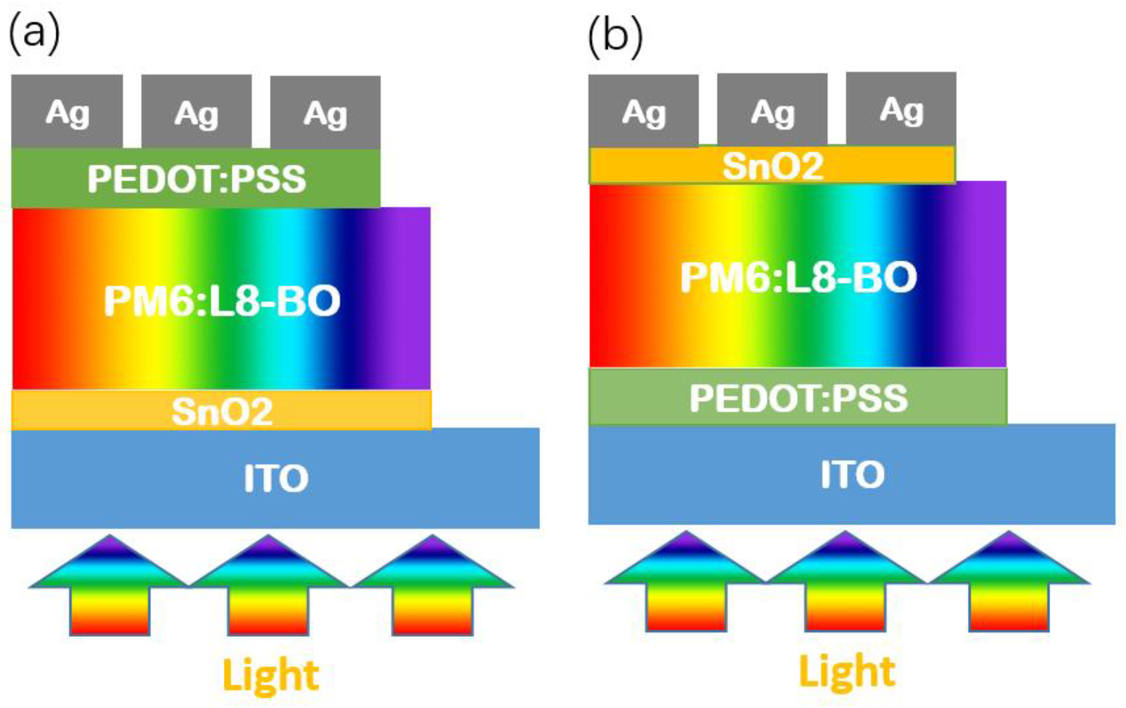
Figure 1. 1D structure of (a) inverted binary organic solar cell; (b) conventional binary organic solar cell structure models under light exposure.
Energies 17 03302 g001
Figure 2. 1D structure of ternary organic solar cell model under light exposure.
Energies 17 03302 g002
Figure 3. (a) Chemical structures of PM6, D18, and L8-BO; (b) external quantum efficiency (EQE) of the devices with different active blend thicknesses; (c) J-V curves of the OSCs based on direct binary, inverted binary, and direct ternary structures with a device area of 4.84 mm2 for each.
Energies 17 03302 g003
Figure 4. Energy levels diagram for ternary organic solar cells.
Energies 17 03302 g004
Figure 5. The distribution of the specter of the absorbed photons of the donor-acceptor (D-A) blends PM6:L8-BO for the direct binary device.
Energies 17 03302 g005
Figure 6. The distribution of the specter of the absorbed photons of the D-A blends PM6:D18:L8-BO for the ternary device.
Energies 17 03302 g006
Figure 7. Charges carrier mobilities. (a) Charge carrier mobility of direct binary, inverted binary, and direct ternary device (direct binary is under-inverted because they have approximately the same measured average mobility) in the function of illumination (a.u.); (b) charge carrier mobility in the function of voltage.
Energies 17 03302 g007
Figure 8. The recombination prefactor of the charges (Kbi) is the function of charge density for the direct, inverted binary, and direct ternary devices.
Energies 17 03302 g008
Table 1. The PCE parameter output of our different devices.
DevicesVoc (v)Jsc (mA/cm2)FF (%)PCE (%)
S1: ITO/PEDOT:PSS/PM6:L8-BO/SnO2/Ag0.85926.580.418.34%
S2: ITO/SnO2/PM6:L8-BO/PEDOT:PSS/Ag0.85926.680.4818.37%
S3: FTO/PEDOT:PSS/PM6:D18:L8-BO/SnO2/Ag0.8926.6582.319.52%
Disclaimer/Publisher’s Note: The statements, opinions and data contained in all publications are solely those of the individual author(s) and contributor(s) and not of MDPI and/or the editor(s). MDPI and/or the editor(s) disclaim responsibility for any injury to people or property resulting from any ideas, methods, instructions or products referred to in the content.