Article

Design Considerations and Experimental Testing of a Wide-Area Inductive Power Transfer (IPT) System for Body-Worn Electronics

1
School of Civil, Aerospace and Design Engineering, University of Bristol, Bristol BS8 1TR, UK
2
School of Electronic, Electrical and Mechanical Engineering, University of Bristol, Bristol BS8 1UB, UK
3
Electronics and Computer Science, University of Southampton, Southampton SO17 1BJ, UK
*
Author to whom correspondence should be addressed.
Energies 2024, 17(14), 3367; https://doi.org/10.3390/en17143367
Submission received: 31 May 2024 / Revised: 1 July 2024 / Accepted: 4 July 2024 / Published: 9 July 2024
(This article belongs to the Section F3: Power Electronics)

Abstract

:
The provision of wireless and battery-free power is key to extending the applications of body-worn sensing electronics. This paper investigates the design of an IPT system for a body-worn scenario where the challenges include highly variable coupling, the requirement for the coil/s to be flexible, and close proximity to the body. Variable coupling results in a system that must operate with received powers ranging over orders of magnitude, whilst the use of flexible coils reduces the Q-factor and results in the potential for inductance variation. The human exposure considerations limit both the maximum field strengths that the wearer of a receiver coil might experience and the field strengths that a third party might be exposed to. In this paper, analytical models are used to identify key design variables and to guide the design synthesis of an IPT system for a wrist-worn medical sensor. Practical circuits to drive the transmit coil and to interface the receive coil with the load electronics are described. A prototype system is tested to validate the theoretical analysis, providing power greater than 2 mW to the sensor over a hemispherical region up to 250 mm in radius from the transmit coil.

1. Introduction

The proliferation of wireless and mobile electronic devices has been paralleled by research efforts to provide them with wireless power. Inductive power transfer (IPT) is a suitable technology for many applications, offering reduced maintenance overheads compared to battery-powered solutions and better availability when compared with energy-harvesting approaches. IPT systems have been realised at power levels from mW to MW, but typically over modest distances due to the sharp decline in near-field magnetic coupling with increasing coil separation.
There is a significant body of published research into IPT, and many commercial de-vices are available. Common applications of IPT include powering technology that can be localised to a charging area, such as the vehicle-charging systems described in [1,2,3], or that can carry a relatively large, rigid receiver system, like the inductive coupler described in [4], or charging systems where the primary coil forms a flat area, e.g., on the surface of a table [5,6]. These systems will typically try to maximise the magnetic coupling between the coils to achieve the best system performance. A system for powering body-worn electronics whilst the wearer sleeps was investigated by Roshan and Park in [7], highlighting some of the challenges of IPT systems with variable lateral and axial misalignments between the coils, which create the conditions of highly variable coupling.
This paper considers an IPT system for powering body-worn electronics where the transmit coil is integrated within an indoor environment, for instance, a seat back or chair arm, and the receive coil is worn on the body, for example, as part of a wrist-worn health sensor, and thus the relative position of the coils is poorly constrained. The highly variable and unpredictable relative position of the transmit and receive coils leads to large changes in the magnetic coupling between the coils. Consequently, this produces large variations in the voltage induced in the receive coil, making the design of the receive-side electronics particularly challenging: if the system is designed for the peak coupling, it may ‘brown-out’ for long periods when the coupling is low; if it is designed for the lowest coupling, then there will be periods when significant excess power must be dissipated on the receive side.
To contextualise the design challenge described in this paper, a dimensional comparison has been performed with previously reported IPT systems. With reference to Figure 1a, showing a cross-section through a two-coil system, the coil separation ‘D’ is divided by the average coil diameter (dTX + dRX)/2 to describe an aspect ratio and then plotted against average coil diameter in Figure 1b. It is useful to consider the aspect ratio rather than the absolute coil sizes, and separation as the aspect ratio, as defined here, is more directly related to the mutual inductance of the coils and can capture the variations in mutual inductance in variable geometry systems. Many systems operate with separation distances equal or less than the coil dimensions (higher-power systems were excluded from the analysis since the aspect ratio is typically very low), and most of these systems have a fixed separation. The system presented in this paper has a varying aspect ratio, which reaches values higher than commonly reported in the literature.
This paper focuses on the design of small load power (mW level), relatively low-cost IPT systems under conditions of highly variable coupling, where efficiency is not an overriding consideration. It is structured as follows. Section 2 reviews IPT theory, setting out equations for the later design; and differences between series-series (SS) and series-parallel (SP) resonant combinations are explored, together with the effects of variable coupling. Section 3 describes the coils, including the relationship between coupling and separation for different size combinations, and considers regulations on human exposure to magnetic fields. Section 4 describes the design of the complete IPT system. Section 5 provides the experimental results, and Section 6 concludes the paper.

2. IPT Theory

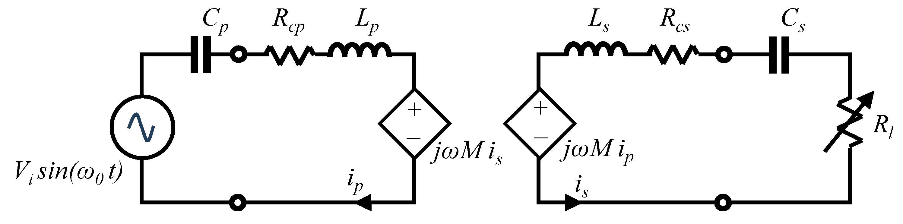
2.1. Tuned-Coupled Circuits—Key Design Parameters

IPT systems typically have primary and secondary coils (denoted as TX and RX, respectively) tuned to resonance. The RX side is made resonant to mitigate the effects of low magnetic coupling due to coil separation/misalignment and the absence of a high-permeability flux path between them [16]. Resonant TX operation reduces the drive VA rating for a given coil excitation as only the real part of the power must be supplied. This arrangement is sometimes referred to as a ‘doubly tuned transformer’, as shown in Figure 2, where the primary and secondary coils (each comprising inductance and parasitic resistance) are coupled by their mutual inductance ( M ), and tuned to resonance by capacitors Cp and Cs, respectively. The resonant circuit on each side can be arranged with either a parallel or series tuning capacitor, with the various possible combinations often described in the literature as ‘series-series’ (SS), ‘series-parallel’ (SP) and so on.
A detailed explanation of the theory of tuned coupled circuits can be found in many reference texts; for example, [17,18,19]. Hence, an overview will be provided, focusing on useful parameters for the later design.
A common approach to analysing the circuit in Figure 2 is to use a postulated impedance, reflected from the secondary and appearing in series with the primary circuit given by:
Z R = ω M 2 Z S e c .    
where ZSec is the impedance of the network formed from Ls, Rcs, Cs and Rl.
With both the primary and secondary circuits in resonance, i.e., 1 L s C s = 1 L p C p = ω o , the reflected impedance becomes resistive (RR) and the primary current can now be derived using:
I P r m s = V i r m s R C P + R R = V i r m s R C P + ω 0 M 2 R c s + R l
The RMS voltage induced in the secondary is given by:
V s r m s = ω 0 M I p r m s = ω 0 M V i r m s R C P + ω 0 M 2 R c s + R l
from which the RMS secondary current is found:
I s r m s = V s R c s + R l = ω 0 M V i r m s R c s + R l R C P + ω 0 M 2 R c s + R l = ω 0 M V i r m s R l R c p + R c p R c s + ω 0 M 2
The secondary voltage in the open circuit can be found by setting R l = , in (3), and the secondary short circuit current by setting R l = 0 in (4). The average power in the load resistance can be derived from I s 2 R l , i.e.,
P R l = ω 0 M V i r m s R l R c p + R c p R c s + ω 0 M 2 2 R l
Equation (5) describes a power response that is non-monotonic with both Rl and ω 0 M , that is to say, for any given ω 0 M there will be a value of Rl that produces the maximum load power and vice versa. The maximum load power occurs when the reflected load resistance is equal to the resistance of the primary coil plus the reflected secondary coil resistance. The condition when maximum power is transferred between the coils is known as ‘critical coupling’ and occurs when the reflected resistance, RR, is equal to the primary coil resistance, Rcp. In common with the design of other transducers, for the best efficiency, the transduction coefficient, ω 0 M , should be maximised, whilst losses Rcp and Rcs should be minimised.
When the coupling between RX and TX coils is low, the primary current, I p , is largely independent of R l and it is often convenient to describe the average load power by:
P R l = ω o M I p r m s R c s + R l 2 R l
The maximum average load power occurs when the load resistance equals the secondary coils resistance and is thus given by:
P R l m a x = ω 0 M I P r m s 2 4 R c s
Commonly, coupling is described by a dimensionless coupling factor k, (where k = 1 implies all of the primary flux couples to the secondary, and k = 0 implies none of the primary flux couples to the secondary), which is defined as:
k = M L p L S
Substituting Equation (8) into (7) yields an expression that can be useful in understanding the design trade-offs:
P R l m a x = ω I p r m s L p 2 k 2 L s 4 R c s
The rate of change of the magnetic flux generated by the TX coil is proportional to ω I p r m s L p , which, importantly, is limited by regulations governing human exposure; k is a geometric measure of coupling into the field; and the quotient L s 4 R c s can be thought of as a ‘figure of merit’ for the RX coil.

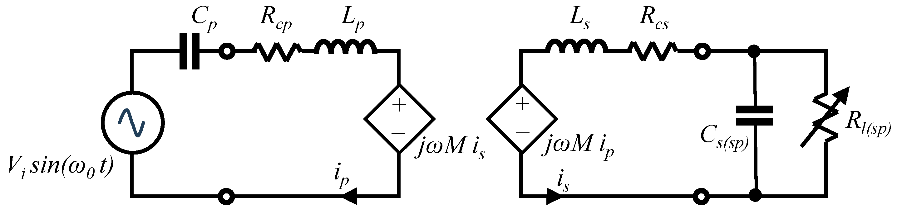
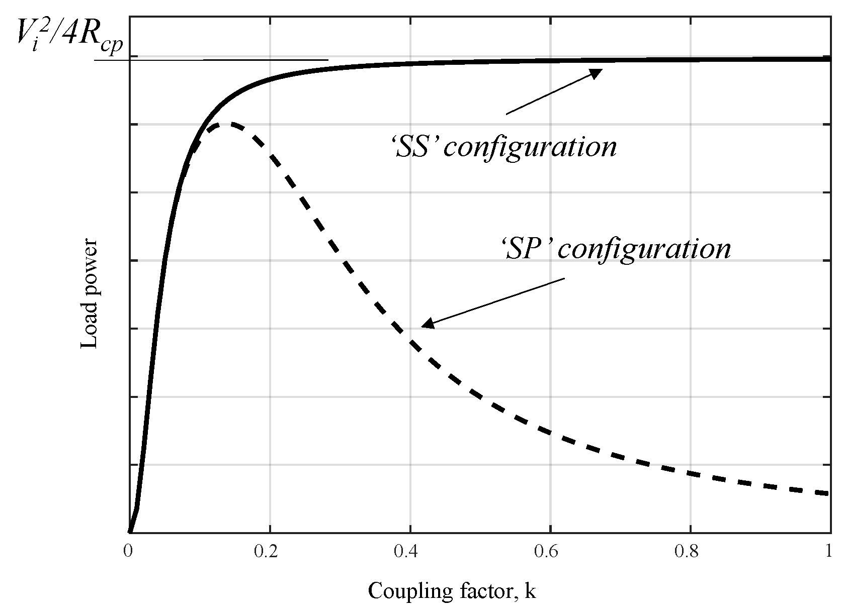
2.2. Series—Parallel (‘SP’) Tuned Circuits

In the case of an ‘SP’ arrangement, as illustrated in Figure 3, analysis may be performed by transforming the parallel load/tuning capacitor into its equivalent series combination using the standard formulae:
R l = R l s p Q l 2 + 1
and
  C s = C s s p ( Q l 2 + 1 ) Q l 2
where Ql is the quality factor of the tuning capacitor and load resistance, given by Q l = R l s p ω 0 C s s p , and the suffix ‘(sp)’ indicates components of the ‘SP’ arrangement. Equation (11) implies that for the secondary tuned circuit to remain in resonance, the value of C s s p must vary with the load resistance. Since this is impracticable, capacitive reactance can be reflected into the primary circuit, resulting in de-tuning; however, this effect, described in several IPT papers (e.g., [20,21]), is negligible at the low coupling levels and correspondingly high Q of interest in this paper.
By the substitution of (10) into (6), the load power in the ‘SP’ case can be expressed as
P R l s p = ω 0 M I P r m s Q s l 2 R l s p
where Q s l is the secondary loaded quality factor given by:
Q s l = ω 0 L s R c s + R l .
Equation (13) illustrates that the voltage across the ‘SP’ load resistance is given by the voltage induced in the secondary magnified by the circuit loaded quality factor (from comparison with P = V 2 R ) and this is congruent with what would be expected from resonant circuit theory. This also illustrates an important conclusion for the comparison of parallel and series RX circuits: the load voltage with the series connection can never be higher than the induced voltage ( ω 0 I P M ), but for the parallel load connection, it is magnified by the loaded secondary quality factor Q s l , and this is advantageous where coupling is low and the induced voltage is insufficient to overcome rectifier voltage drop. Some care is needed when considering Equation (12) since R l s p and Q s l are not independent.

2.3. Optimum Load for Maximum Power Transfer with Variable Coupling

Achieving maximum power to the load is normally the goal of IPT systems. Figure 4 shows how the optimum load resistance varies with coupling factor, and Figure 5 shows how the power in the optimum load resistance varies with the coupling. The load is assumed to be purely resistive and the tuning capacitors are fixed and tuned to resonate with the coils at the excitation frequency, i.e., 1 L p C p = 1 L s C s = ω 0 . Both figures are derived from numerical simulation of the equations already presented, with parameter values taken from later in this paper. The curves are shown here to illustrate the qualitative trend, so the values from the numerical simulation are omitted; however, algebraic expressions for the optimum load resistance at k = 0 and k = 1 (noting that these are not exact in the ‘SP’ case as the full expressions are longwinded) are provided in Figure 4 and an expression for the maximum load power in the ‘SS’ case when k = 1 is indicated on Figure 5. The analysis assumes Vi is kept constant.
Figure 4 illustrates how the optimum load in the ‘SS’ becomes very small at low coupling levels (tending to the secondary coil resistance at k = 0) but that in the ‘SP’ case it follows the opposite trend, becoming smaller as coupling increases and tending to the secondary coil reactance. From Figure 5, it is seen that the rise in the load power for the series and parallel cases tracks as the coupling increases up to approximately k = 0.1, but above k = 0.1, the load power for the parallel connection starts to fall. This is explained by the aforementioned capacitive reactance reflected back to the primary from a parallel resonant secondary at higher levels of damping (i.e., lower Qsl).

2.4. Operation with a Peak Rectifier
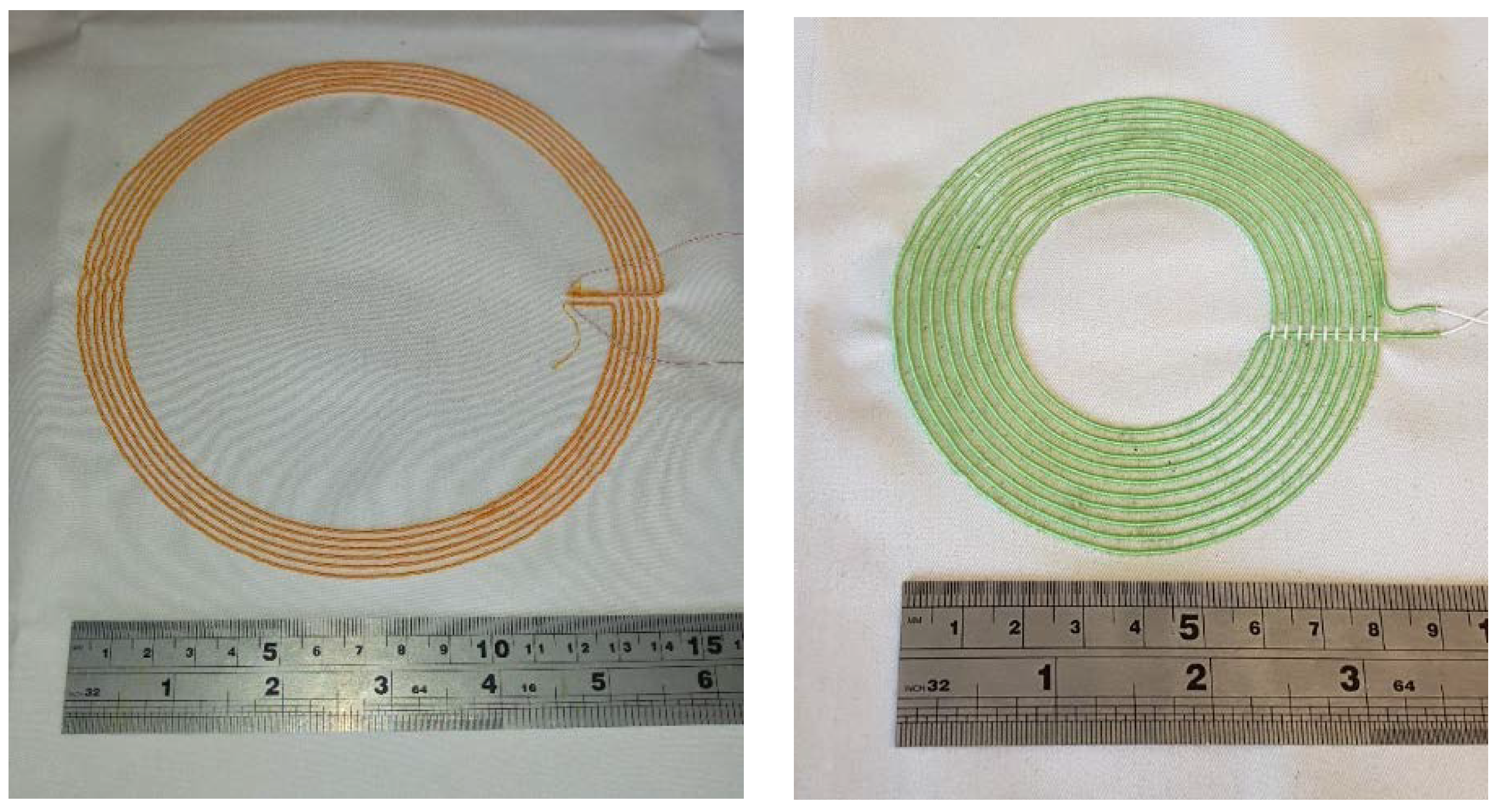
A common load for an IPT system will be a peak rectifier (i.e., rectifier followed by reservoir capacitor), which introduces harmonics. A non-resonant transformer would have its utility factor derated to the rectifier power factor, approximately 0.7 for a full-wave rectifier and 0.35 for half-wave [22], to cope with the losses incurred by these harmonics. However, in the case of the ‘SP’ IPT arrangement, the tuning capacitor provides a low impedance shunt path for the current harmonics. In addition, the secondary coil current is dominated by the recirculating component of the tuned circuit, and the losses are predominately due to this over any load component. Hence, the ‘SP’ IPT system is insensitive to the non-linearity of a rectifier load. The action of a peak rectifier results in a DC load voltage √2 higher than the rms level of the AC input voltage (assuming no diode forward drop); therefore, the optimum load with a rectifier will be approximately doubled compared to that where a resistive load is supplied directly.
In the ‘SS’ case, a peak rectifier behaves differently: the rectifier becomes part of the series resonant circuit, forcing the rectifier input current to be sinusoidal and the input voltage to be a square wave with an amplitude equal to the load voltage. An analysis of this can be found in [23].

3. TX and RX Coils

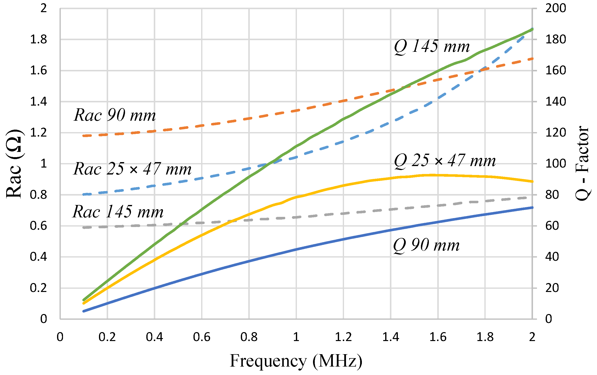
3.1. Coil Design and Properties

The aim in coil design is to maximise the coupling, i.e., ω 0 k L p L s , whilst minimising the parasitic losses (which can be broadened to include the capacitor ESR as well as coil resistance). For air-cored coils, a higher inductance coil implies a larger diameter, with more turns; however, physical size restrictions may limit the diameter, and increasing the inductance requires the size of the tuning capacitor to be reduced for a given frequency, which at some point becomes impractical due to the stray capacitance of the coil and connecting leads and/or the ESR of the capacitor becoming significant.
The IPT system described in this paper employs a flexible construction for the TX coil, allowing it to be incorporated into soft furnishings or clothing. The coil is constructed using flexible wire that is machine-embroidered in a spiral onto a light canvas sheet, as shown in Figure 6. This manufacturing technique, which trades a copper cross-section for flexibility, results in lower native quality factors (ωL/ R a c ) than could be achieved with rigid coils of a similar geometry.
Some variation in the TX coil diameter can be accommodated, so two different-sized prototypes were constructed with outside diameters of 90 mm and 145 mm to explore the differing coupling characteristics with separation (described in Section 3). The number of turns in each coil is chosen to produce an inductance in the region of 10 µH. The 90 mm coil, Figure 6a, had 10 turns of 7 × 0.08 mm PTFE-insulated wire, an inductance of 9.8 µH and a DC resistance of 1.2 Ω. The 145 mm coil, Figure 6b, had 6 turns of 81/0.04 Litz wire (81 strands of 0.04 mm enamelled copper wire), an inductance of 12.2 µH, and a DC resistance of 0.57 Ω. The use of Litz wire allowed an increase in the copper cross-section without reducing the flexibility. A key advantage of lower TX coil resistance lies in the reduction of the heat generated for a given current. It was found empirically that a current level of the 2 Arms would result in an acceptable temperature rise (i.e., warm to the touch) when the 90 mm coil was mounted with one side well-insulated and one exposed to the air at ambient temperature.
The RX coil is designed to be incorporated into a rigid wrist-worn sensor package that has inside dimensions of 25 × 47 mm, and hence, it is tightly constrained in size. It is of more conventional construction, using 10 turns of 36/0.04 mm Litz wire formed into a rectangular shape inside the periphery of the case for the maximum induced voltage per turn, resulting in an inductance of 12.5 µH with an DC resistance of 0.8 Ω, and it is shown later in the paper in Section 4.4. A ferrite backing is incorporated to shield it from the ground plane of an adjacent circuit board.
The properties of the coils, as measured using a Wayne Kerr 6500B analyser (https://www.waynekerrtest.com/products_detail.php?indexs=4, accessed on 3 July 2024), are shown in Figure 7. The rise in the coil resistance with the frequency due to skin and proximity effects [24,25] limits the rise in the native quality factor with the frequency. In addition, adding the ferrite backing to the RX coil introduces an additional frequency-dependent loss.

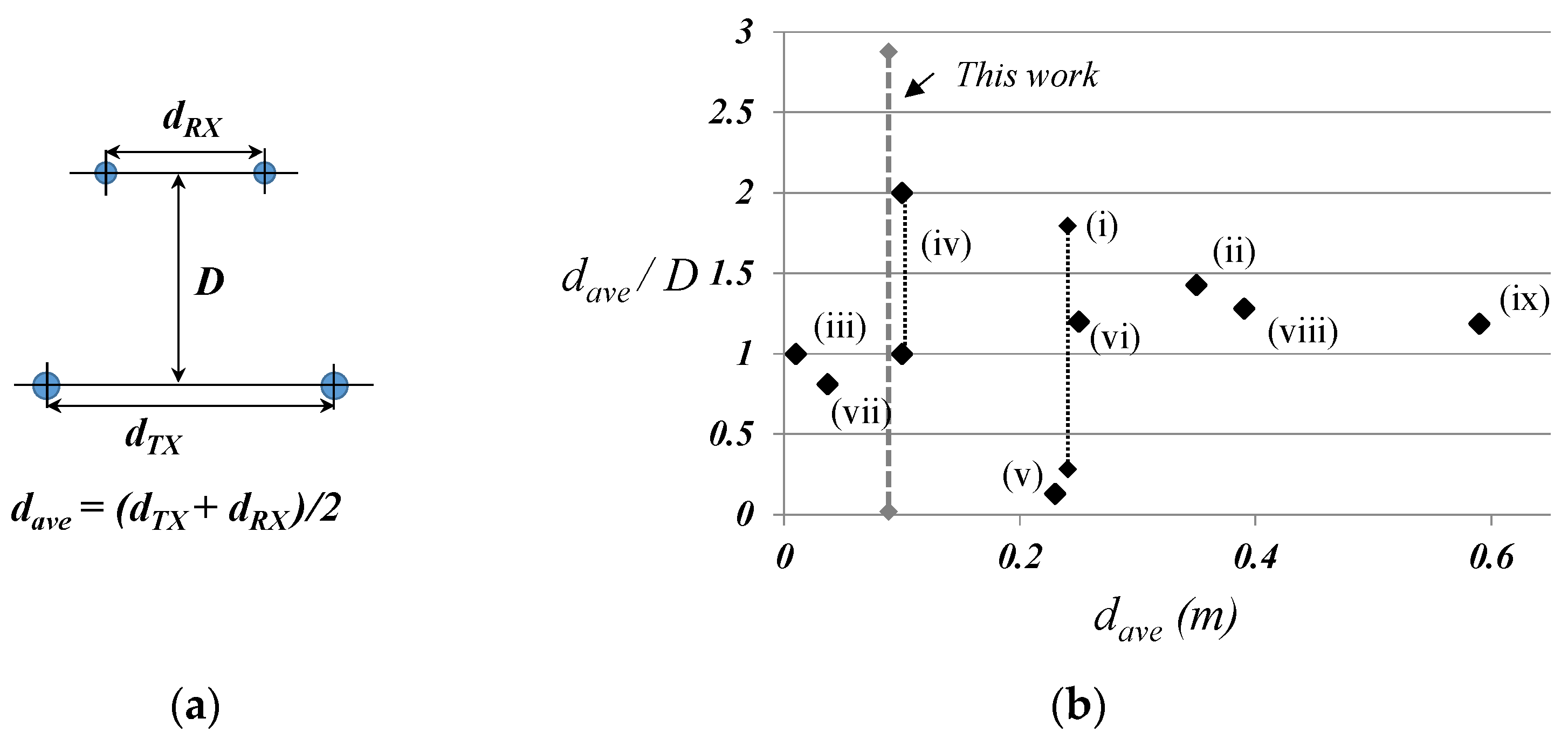
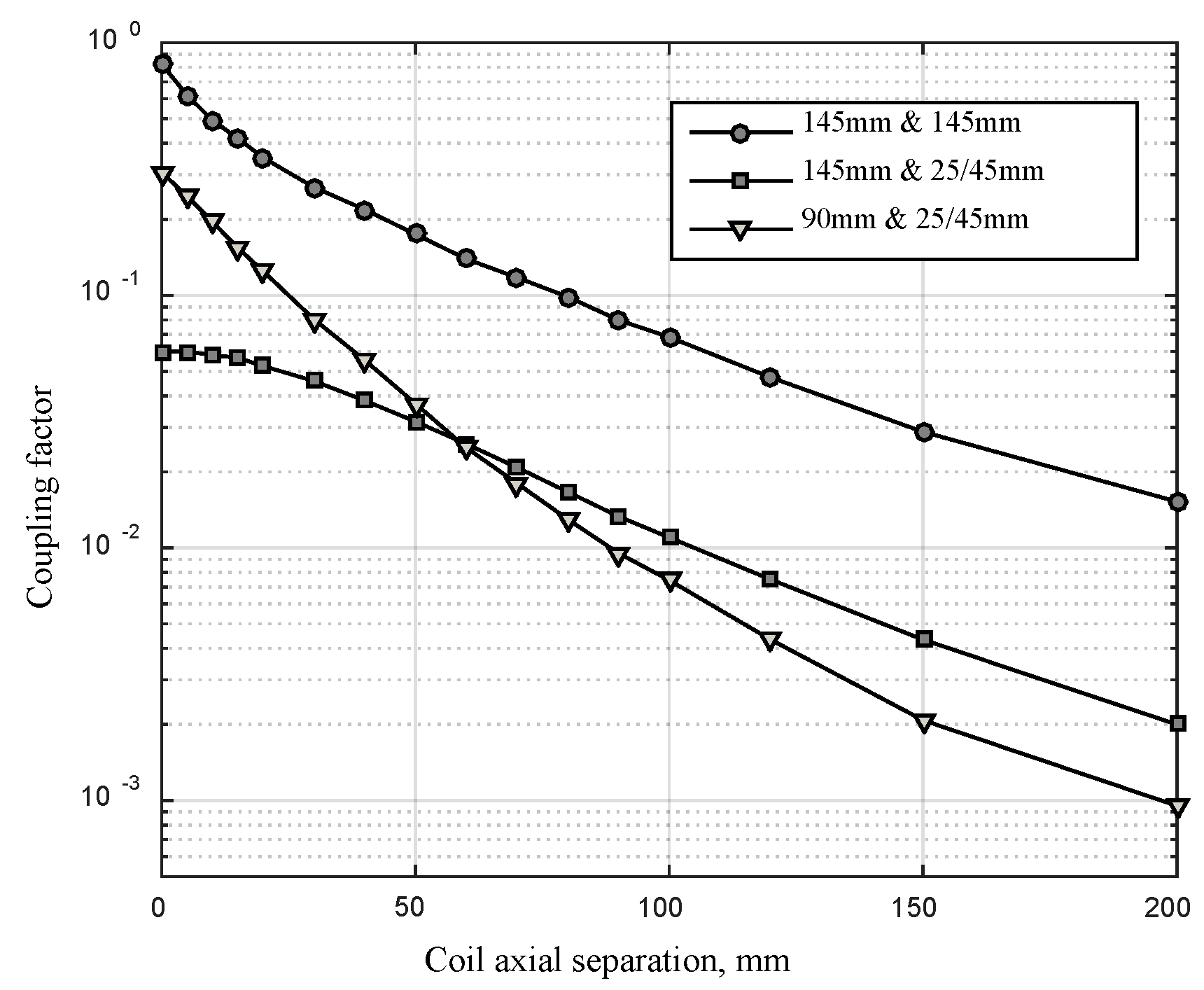
3.2. Influence of Coil Separation on Coupling and Choice of Load

Mathematical derivations of the coupling between coils have been published, for example, the analytical expressions in [26], considering geometric and material parameters, as have numerical tables to determine the mutual inductance in [27]. However, analytical approaches are not trivial, and a significant body of literature uses empirical or numerical results, for example, in [8], where numerical simulation is used, and a comparison is performed of the transmission efficiency with various combinations of shapes and sizes of transmit and receive coils.
Figure 8 shows the coupling factor between three combinations of coil pairs, measured experimentally, over various axial separations. The three coil pairs were: (i) 145 mm TX and 145 mm RX; (ii) 145 mm TX and 25 × 47 mm RX; and (iii) 90 mm TX and 25 × 47 mm RX. High coupling factors are only achieved between the similarly sized coil pairs when closely spaced. The coupling factor between the differently sized pairs (ii and iii) crosses over at ~60 mm separation. This occurs because at zero axial separation the coupling factor is highest when the ratio of coil areas is unity (i.e., same diameter coils give best coupling), whereas at larger separations the combined total of the areas dominates. To minimise variations in the received power, there is an advantage in constructing an IPT system that must operate over a range of coil separations to have a large TX coil and a smaller RX coil.
Using the analysis presented in Section 2 and the results from Figure 8, the plots in Figure 9 show the optimum load resistance (for the maximum load power) against the coil separation for the 145 mm TX/25 × 47 mm RX coil pair in the ‘SS’ and ‘SP’ arrangements. The coupling is low for all the separations above a few tens of millimetres; hence, the optimal load resistance for the ‘SP’ case is high for all the separations, tending to a fixed value as separation increases. In contrast, the optimal load in the ‘SS’ is very low, tending to a value below 1 Ohm as the separation increases, and the low load voltages implied would make rectification inefficient.
Figure 10 shows a comparison of the load power in the ‘SP’ case for a fixed value of 1800 Ω compared to the maximum that could be achieved with a variable optimum load. A fixed load resistance matching the optimal value at large separations produces close-to-optimal performance over most of the range and additionally reduces the min–max power over all the separations.

3.3. Compliance with Human Exposure Guidelines

An IPT system designed to power body-worn equipment implies the possibility of the close proximity of people and the coils. Human exposure to time-varying magnetic fields must be limited to prevent electrostimulation and/or heating of tissue, and these are set out in the ICNIRP guidelines [28] and IEEE standard C95.1 [29]. A 2D axisymmetric finite element model was used to approximate the effect of the 145 mm TX coil on adjacent tissue. The coil was assumed to have free space on one side and a homogeneous region of tissue on the other, and a conductivity of 0.45 Sm−1 was modelled to represent muscle at 500 kHz. The coil current was set at 2 Arms.
Due to the relatively small extent of the magnetic field, the SAR limits were easily met with a coil current of 2 Arms; the highest SAR level (averaged over 10 g of contiguous tissue) was found to be 0.1 Wkg−1, compared with ICNICP limits of 2 Wkg−1 for the head and trunk and 4 Wkg−1 for the limbs (general public exposure).
The electrostimulation limits are potentially more significant, with the ICNIRP guidelines specifying a maximum induced current density of 1 Am−2 for general public exposure and 5 Am−2 for occupational exposure. With a coil current of 2 Arms at 500 kHz, the occupation limit was exceeded for distances less than 14 mm from the conductors, and the general public limit was exceeded when less than 73 mm from the conductors. The IEEE guidelines state a maximum magnetic field strength of 163 Am−1 for general public exposure, which is exceeded at 7 mm from the coil conductors, and an occupational limit of 490 Am−1, which is never exceeded. The apparent anomaly between these standards is likely because in this paper the tissue is modelled as muscle, which has a relatively high conductivity compared to other tissues and thus represents a worst case for induced current; if the conductivity is 0.045 Sm−1 (i.e., the value for fat), then the maximum induced current density in tissue adjacent to the coil is 0.7 Am−2.
These initial results suggest that SAR is unlikely to be a limiting factor but that magnetic field strengths and the associated induced currents need to be carefully considered. Further discussion on human exposure issues can be found in a review paper by Hui [30].

4. Implementation

4.1. System Design Discussion

The design process for an IPT system starts with the high-level requirements of the power to be transmitted over a given range, and it is constrained by physical geometry, field intensity limitations, and electrical system constraints.
The choice between series and parallel resonant topologies is largely influenced by the drive electronics and load considerations. For example, consider driving the TX coil: a parallel resonant arrangement requires the drive electronics to support the full coil voltage (which may be 10’s or 100’s of volts) but at a low current; with a series circuit, this is reversed. In addition, the series circuit presents a high impedance to the harmonics of the resonant frequency, allowing simple voltage switching circuits such as Class D to be used, whereas a parallel circuit necessitates pure sinusoidal voltage excitation. Series tuning of the RX allows for a load voltage no higher than the induced voltage ( ω 0 I P M ) , noting that in the application described here the induced voltage is less than 0.2 V at the extremes of coil separation, which is impractical to rectify. With parallel tuning, the load voltage is magnified by the secondary loaded quality factor.
The choice of operating frequency is inextricably bound to the TX driver circuit design, properties of the coils, and human exposure limits. IPT design should seek to maximise the coupling, ω 0 k L p L s ; however, the frequency cannot be always be increased since if it is assumed that a particular TX coil is operating at the limit of the human exposure, then the product ω I p r m s cannot be further increased, compounding any frequency restrictions imposed by practical tuning capacitor values described in Section 2 The rise in the coil AC resistance with the frequency further limits the utility of ever-higher frequencies.
Class-E power circuits can operate well above 1 MHz [12]; however, a careful match to the load is required for high efficiency. Flexible coils provide the potential for variation in the inductance and thus in the resonant frequency of the tuned circuits. This potential variability steers the choice of driver circuit towards Class D, which is more tolerant in this respect but does limit the practical upper operating frequency due to switching losses. Allied to this, a further advantage of Class D is the ability to easily vary the frequency, for example, to modulate the power as in the commercial QI IPT standard.

4.2. Transmit Coil Drive Circuit

The TX drive circuit is shown in Figure 11. The MOSFET driver U1 provides differential drive to the gate-drive transformer. MOSFETS Q1 and Q2 form a half-bridge, switching one end of the TX coil between V+ and ground. The tuning capacitor C2 performs the additional function of DC blocking. The series-tuned circuit presents a low resistive load to the fundamental of the square wave voltage but a high inductive reactance to the harmonics, resulting in a near-sinusoidal current waveform. The effective driving voltage (i.e., V i r m s ) in Section 2 is 0.45 Vs.
The topology of Figure 11 is typically found in converters switching at ~100 kHz [31]. Operation at 500 kHz–1 MHz requires careful MOSFET selection, trading between on-state resistance and gate charge. In this prototype, IRFR120N devices are used with an RDS(on) of 0.2 Ω, and 25 nC gate-charge. The gate-drive transformer is wound on a 13 mm diameter ferrite toroid (TN13/7.5/5-3C90), each winding 25 turns of 0.2 mm wire. The compact layout of the gate-drive circuit and trifilar windings along with the 10 Ω gate resistors are used to reduce the ringing. No dead time is intentionally introduced, but no evidence of shoot through is observed. The tuning capacitor comprises 1600 Vdc-rated polypropylene-film capacitors of 3.3 nF and 4.7 nF in parallel. These are high-stress components carrying the primary current and sustaining a peak voltage of over 100 V at 500 kHz, requiring careful study of the manufacturer’s frequency-derating curves for reliable operation [32].

4.3. Receive Circuit and Power-Conditioning

The load in the target application of this IPT system is a wearable sensor incorporating a microprocessor and radio transmitter, described in more detail in [33]. The power demand is highly duty-cycled and may be adjusted by altering the sampling and transmission rates; however, a ‘worse case’ of 1 mW average is assumed for the IPT design. It is desirable that the device can operate for a period without direct powering by the IPT system; hence, some energy storage is required. The design target for the IPT system is to provide 2 mW of power at a coupling factor equivalent to an axial coil separation of 200 mm, allowing for the operation of the wearable sensor and the charging of a local energy store.
Figure 12 shows the complete receive-side power circuit, comprising a tapped RX coil, with tuning capacitor, Cs; a half-wave peak rectifier using a 1N5818 Schottky diode Drect and capacitor Cres; a 12 V Zener diode clamp, Dclamp; a flyback converter operating at fixed frequency in discontinuous inductor current mode; a 5.5 V shunt regulator; and a supercapacitor Cstore.
For an ‘SP’ connection at 500 KHz, the optimum load is ~1800 Ω, and it is doubled to 3600 Ω by the peak rectifier. This presents some difficulties for the design of the converter, requiring a high value of inductance that cannot be accommodated within the wearable sensor enclosure. To overcome this, the rectifier is fed from a centre tap on the coil, which reduces the optimum load resistance by the square of the ratio N2/(N1 + N2), in this case by a factor of four, to 900 Ω.
The tuning capacitor is formed from combinations of surface-mounted 1206--size ceramic COG types, and an ESR less than one-tenth of the coil resistance is achieved. It is difficult to achieve identical resonant frequencies in the TX and RX tuned circuits, and it is found advantageous to adjust the drive frequency to match the receive circuit.
The half-wave rectifier saves a diode forward drop compared to a full-wave arrangement, which is beneficial at low coupling; the rectified output of the receive circuit is clamped at 12 V by the Zener shunt to protect the tuning capacitor, rectifier diode and following circuits at high coupling (voltages up to 60 V are otherwise developed). The clamp limits the maximum power to 160 mW, which will nevertheless charge the 0.47 F supercapacitor in a little under 1 min. The damping effect of the clamp also reduces the current circulating in the tuned circuit at higher coupling. It can be imagined that the choices of the voltage clamp level and coil tap position are a compromise between performances at differing coupling levels. Dealing with the power dissipated in the shunt during periods of high coupling is found to be a key practical challenge for this system and requires the voltage clamp components to be thoughtfully positioned on the circuit board to prevent localised heating.
The flyback converter operates at a fixed frequency in discontinuous mode and presents a ‘resistive’ load to the rectifier, adjusted to 900 Ω; the authors have reported similar designs in [34], hence it is not shown here. The output is fed into a supercapacitor, Cstore, which is clamped by a shunt regulator to 5.5 V.

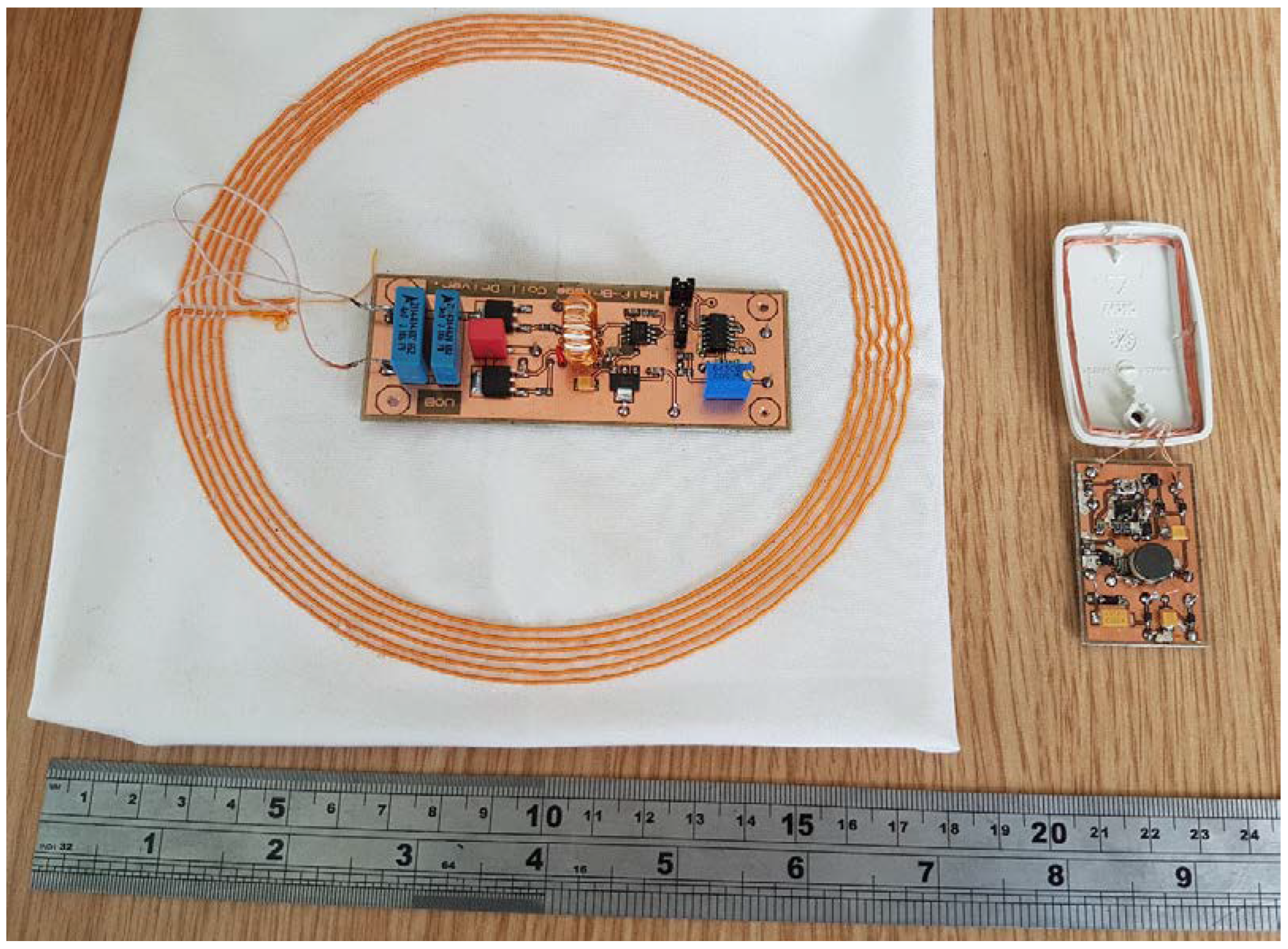
4.4. Complete System

The complete IPT system is pictured in Figure 13, including the drive circuit with the 145 mm TX coil; the receive coil in its housing (with ferrite backing and wearable sensor removed for clarity) and the receive side power-conditioning board.

5. Experimental Results

5.1. Load Power Plots

A series of experimental tests was performed to validate the theoretical model presented in Section 2and to illustrate the maximum range of the system when powering the electronic load. An ‘SP’ tuning arrangement is used throughout, and the TX coil is driven with the circuit of Figure 11, with the supply voltage set to produce a current of 2 Arms in the coil at 500 kHz, with the RX coil removed by a long distance, i.e., zero coupling. Being a voltage source drive, the voltage remains constant during the experiment, but the resulting reflected resistance causes the TX coil current to be modulated.

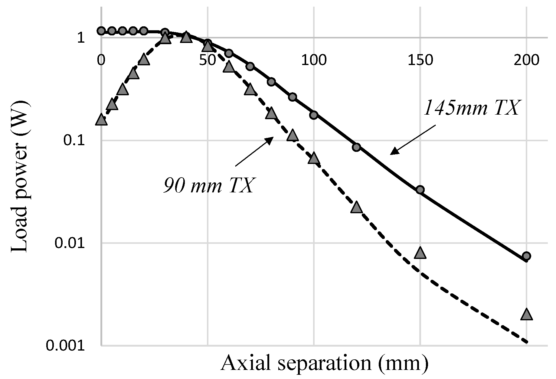
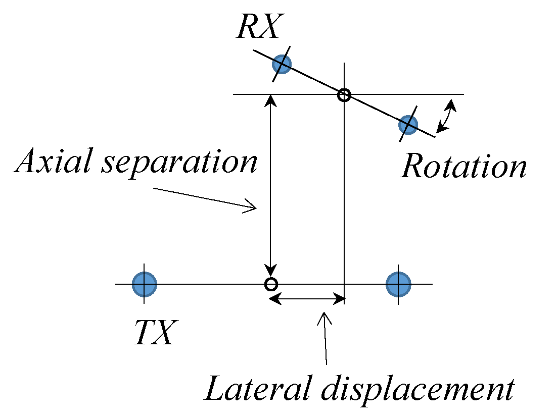
5.2. AC Load (No Rectifier) Power versus Axial Separation and Lateral Misalignment

The power developed in a fixed load resistance on the output of the RX resonant circuit (AC side) for various relative coil positions was compared for the two TX/RX coil combinations: 90 mm TX/25 × 47 mm RX and 145 mm TX/25 × 47 mm RX. The load resistance is a fixed value of 1800 Ω and the RX coil has a ferrite backing in place.
Figure 14 shows the result for axial separations. The markers indicate experimentally measured points and the lines derived from numerical simulation. The experiments show good agreement with the analytical results and confirm the behaviour predicted earlier, i.e., that the smaller TX coil achieves critical coupling at around 40 mm separation, but that the larger TX coil always remains below critical coupling. As illustrated in Section 2 the consequence of this is that the 145 mm TX/25 × 47 mm RX combination would see negligible benefit from introducing a variable load. Also apparent is the advantage of using the larger 145 mm TX coil when maximum range is the goal, with the load power at 200 mm separation being 3.75 times that available with the 90 mm TX coil.
Figure 15 shows the experimental results of the load power against the lateral misalignment of the coil pairs at an axial separation of 200 mm. The two TX/RX combinations show a similar trend, with the larger 145 mm coil combination maintaining substantially higher load power over the range tested.

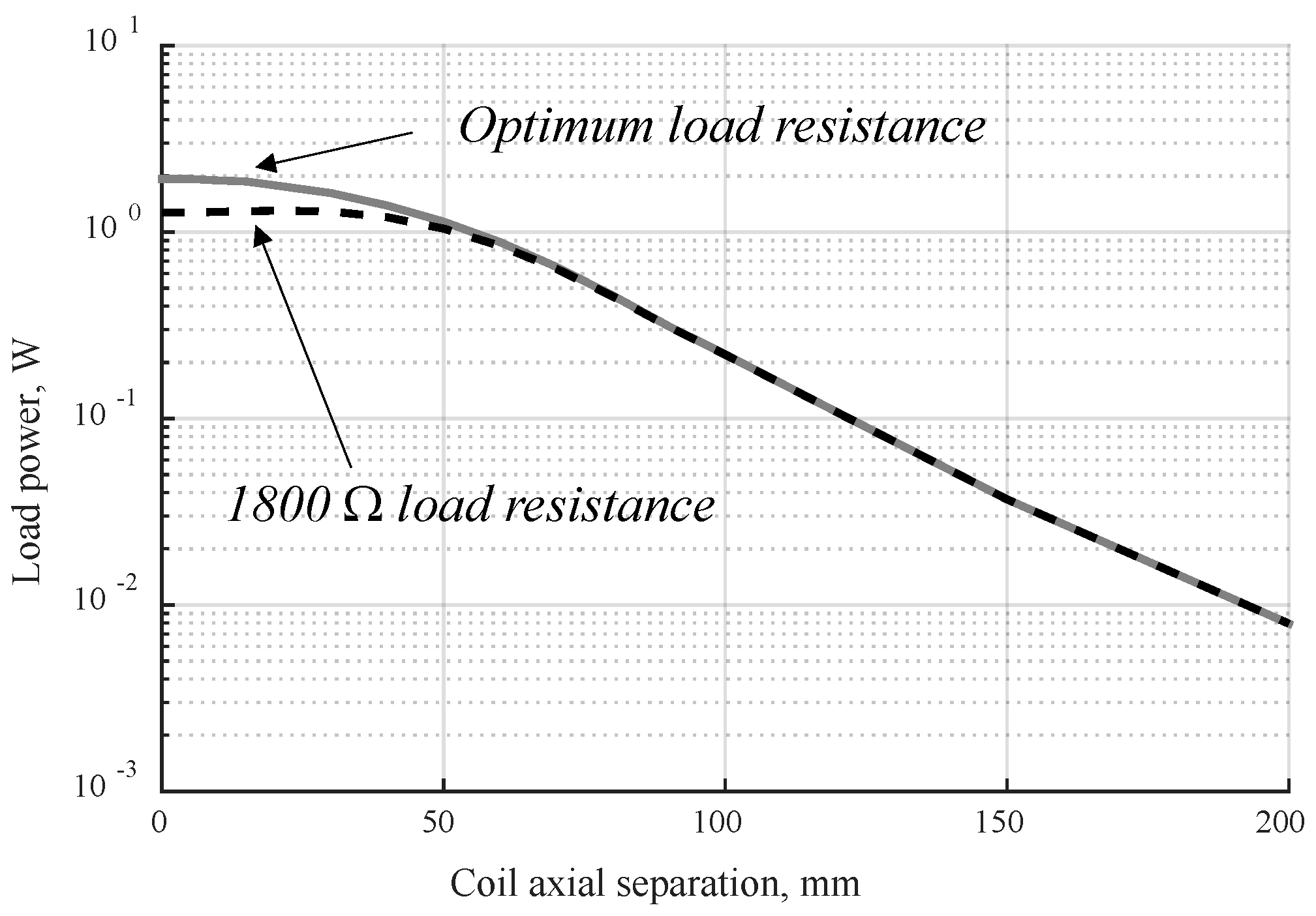
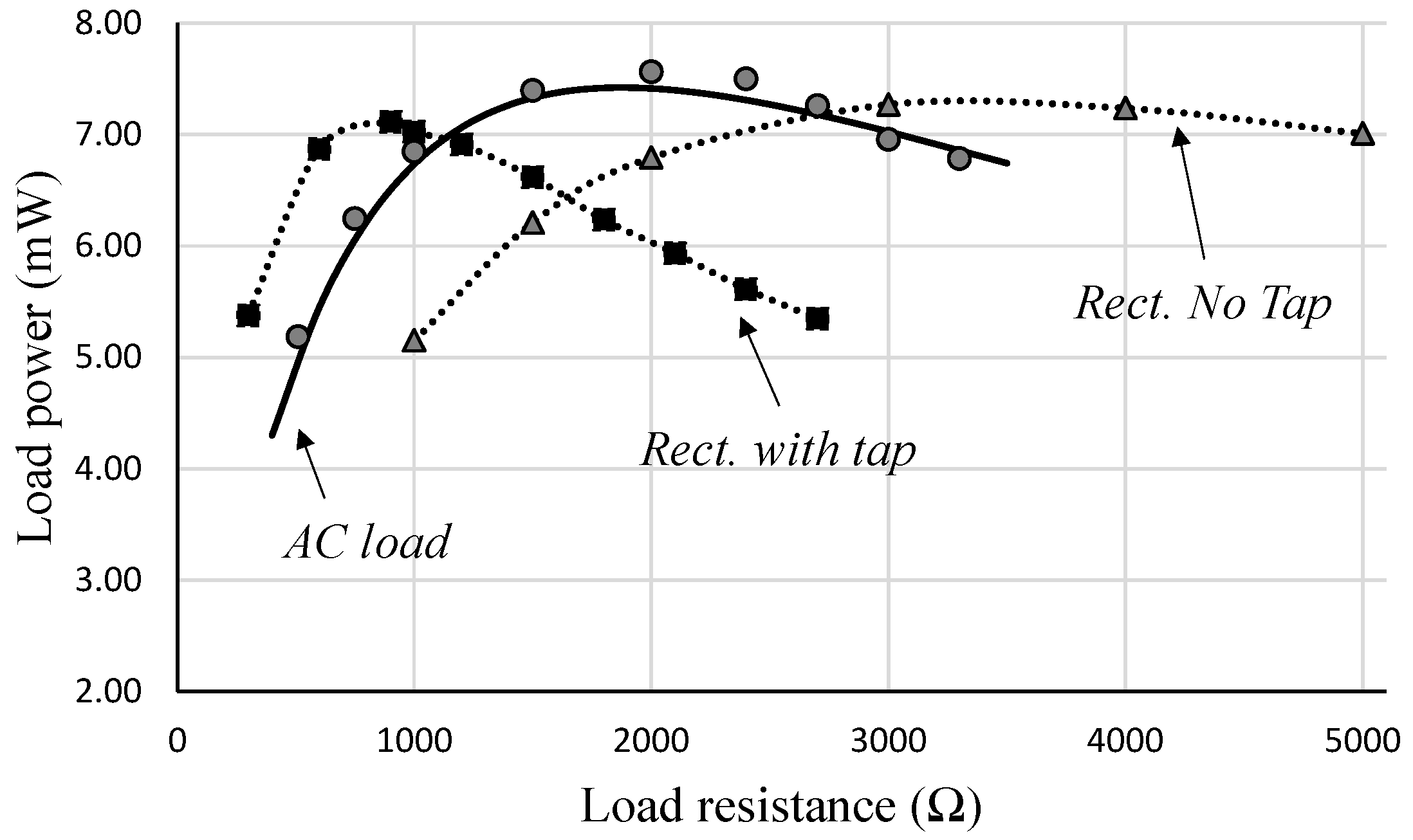
5.3. DC Load Power (with Rectifier) and Optimum Load at 200 mm Axial Separation

The 145 mm TX/25 × 47 mm RX combination with the coils spaced at 200 mm and zero lateral displacement was used to explore the effects of the rectifier and RX coil tap on the load power. The results are shown in Figure 16. First, the power into a load resistance on the AC side, directly across the full RX coil, was measured. Then, the power developed in a DC side load (a physical resistor across the reservoir capacitor, Cstore, of Figure 12) was measured both with and without the coil tap. As expected, the rectifier causes the optimum load resistance to approximately double compared to the AC case, and the centre tap causes the optimum load to be reduced to a quarter of that when supplied across the whole coil, i.e., approximately 900 Ω as opposed to 3600 Ω. The peak load power is reduced in both cases using the rectifier, and this is almost entirely due to the forward voltage drop of rectifier diode rather than harmonic current losses.

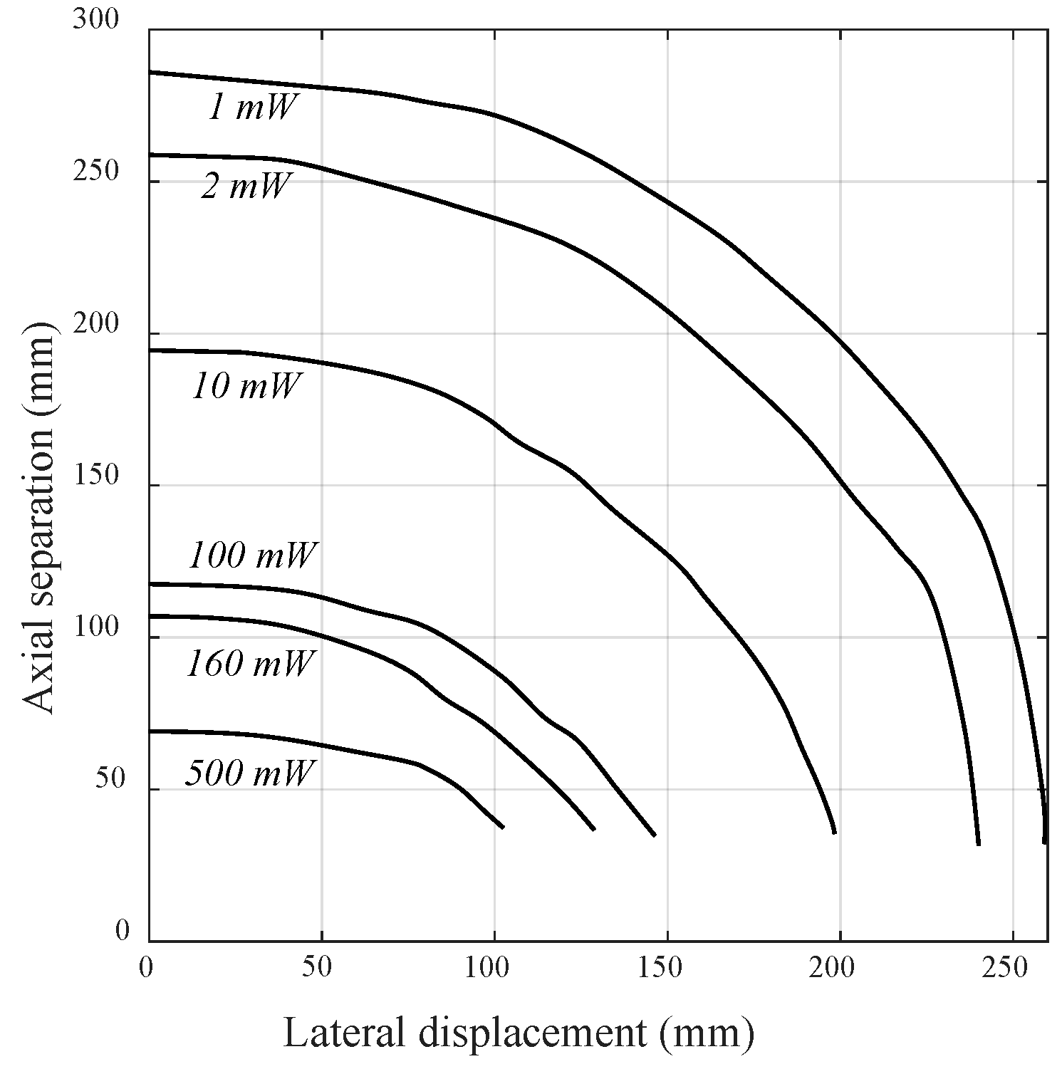
5.4. Power Spatial Envelope Tests

The TX coil was fixed horizontally and the RX coil mounted on a dual axis-positioning frame, allowing the centroids of the coils to be relatively displaced in the vertical and lateral directions over a 0–300 mm range in 20 mm increments; additionally, the RX coil could be rotated about the axis perpendicular to the axes of displacement, as illustrated in Figure 17. The RX coil is loaded with the rectifier circuit of Figure 14, with a DC load resistance of 3600 Ω. To fully explore the power envelope, the voltage clamp and converter were omitted and a silicon rectifier diode substituted when the load voltage exceeded ~20 Vdc. In the first test, the RX coil was kept horizontal (no rotation) and the DC load power measured as the coil was moved to fixed positions (Figure 18); in the second test, the RX coil was rotated at each position to achieve the maximum power (Figure 19).
Both Figure 18 and Figure 19 plot contours that would be expected from the magnetic flux line produced by the TX coil. The null that appears in Figure 18 indicates the regions in which the flux lines are horizontal (with the TX coil in this orientation); in these regions in Figure 19, the coil has been rotated through 90 degrees to achieve maximum coupling. It is, of course, possible to rotate the RX coil to produce zero power at any particular location.

5.5. System Power Consumption and Losses

The worst-case power consumption of the driver is when the RX coil is out of coupling, and in this condition, with the TX coil current at 2 Arms, the DC supply was 0.9 A and 4.35 V, giving a value of 3.9 W for the maximum system input power. When the received coil was brought to close coupling, the measured supply current reduced by 50% to 0.45 A, giving the lowest system input power of 1.96 W. With a maximum output power limited to 160 mW by the shunt, the maximum end-to-end system efficiency is then 8.2%. Since 3.9 W is dissipated by the TX side circuitry when the RX side is out of coupling, consideration must be given to packaging the TX side components, especially if they are to be housed within, or have the potential to be covered by, insulating materials.
The efficiency of the fly-back converter alone was measured at four output power levels: 1 mW, 2 mW, 10 mW and 125.4 mW, which provided efficiencies of 81.8%; 86.2%; 87.7% and 84.2%, respectively.
With the coils in maximum coupling, the worst-case dissipation of 0.79 W was measured in the shunt regulator and 0.24 W in the RX coil, reinforcing the need for careful thermal design on both the TX and RX sides.

6. Conclusions

This paper has demonstrated the design and implementation of a practical IPT system delivering mW-level power for body-worn applications. The use of flexible TX coils did not significantly compromise the system operation, as might have first been thought. The wide range of coil coupling over which the system was designed to operate, which translated into a hemispherical separation of over 250 mm radius (when favourably aligned), meant that the efficiency of the power transfer could become very low. However, the authors suggest it is unhelpful to judge low-power, wide-range IPT systems solely in terms of the efficiency and better to think in terms of the functionality for a particular input power to the system—for example, this system can provide 2 mW over a 250 mm hemisphere for a input power of 3.9 W.
In applications with a very wide range of coupling, there is a clear advantage in using the ‘SP’ resonant arrangement, primarily in order to provide sufficient voltage for rectification at low couplings. However, the ‘SP’ arrangement results in high conduction losses in the secondary coil during periods of high coupling even when no load power is drawn. The ‘SP’ arrangement places more stress on the tuning capacitor and a voltage clamp is required to protect the tuning capacitor itself, rectifier diode and downstream electronics; it also dissipates significant power under highly coupled conditions. In common with current commercial IPT systems, this issue could be addressed by implementing some form of ‘intelligence’: communications back from the receiver to the transmitter to modulate the power, as described in [32], or by using the packaging of the TX coil to physically prevent very-high-coupling scenarios.
The regulatory limits concerning human exposure to magnetic fields are shown to be a consideration for IPT systems at this power level, suggesting that this is an appropriate area for further investigation. Published work on a similar application for IPT systems, albeit with a lower range of variable coupling [7], does not include sufficient experimental results to allow for a full comparison between the systems and the overall scarcity of compete system descriptions in the literature indicates that there is still significant work to do on IPT for body-worn sensing and suggests that the analysis and practical results provided in this paper will be useful for other researchers to build upon.

Author Contributions

Conceptualization, S.B. (Steve Burrow); Methodology, S.B. (Steve Burrow); Validation, L.C.; Formal analysis, S.B. (Steve Burrow) and L.C.; Investigation, S.B. (Steve Burrow), L.C., B.S. and S.B. (Steve Beeby); Resources, B.S., S.B. (Steve Beeby) and N.G.; Writing—original draft, S.B. (Steve Burrow); Writing—review & editing, L.C. All authors have read and agreed to the published version of the manuscript.

Funding

S. Beeby and B. Stark would like to acknowledge the support of EPSRC, grant EP/K031910/1.

Data Availability Statement

The original contributions presented in the study are included in the article, further inquiries can be directed to the corresponding author.

Conflicts of Interest

The authors declare no conflict of interest.

References

  1. Budhia, M.L.; Covic, G.A.; Boys, J. Design and Optimization of Circular Magnetic Structures for Lumped Inductive Power Transfer Systems. IEEE Trans. Power Electron. 2011, 26, 3096–3108. [Google Scholar] [CrossRef]
  2. Aydin, E.; Aydemir, M.T.; Aksoz, A.; El Baghdadi, M.; Hegazy, O. Inductive Power Transfer for Electric Vehicle Charging Applications: A Comprehensive Review. Energies 2022, 15, 4962. [Google Scholar] [CrossRef]
  3. Jayalath, S.; Khan, M. Design, Challenges, and Trends of Inductive Power Transfer Couplers for Electric Vehicles: A Review. IEEE J. Emerg. Sel. Top. Power Electron. 2020, 9, 6196–6218. [Google Scholar] [CrossRef]
  4. Sergeant, P.; Van Den Bossche, A. Inductive coupler for contactless power transmission. IET Electr. Power Appl. 2008, 2, 1–7. [Google Scholar] [CrossRef]
  5. Hui, S.R.; Ho, W.W. A New Generation of Universal Contactless Battery Charging Platform for Portable Consumer Electronic Equipment. IEEE Trans. Power Electron. 2005, 20, 620–627. [Google Scholar] [CrossRef]
  6. Liu, X.; Hui, S.Y. Optimal Design of a Hybrid Winding Structure for Planar Contactless Battery Charging Platform. IEEE Trans. Power Electron. 2008, 23, 455–463. [Google Scholar]
  7. Roshan, Y.M.; Park, E.J. Design approach for a wireless power transfer system for wristband wearable devices. IET Power Electron. 2017, 10, 931–937. [Google Scholar] [CrossRef]
  8. Choi, J.; Seo, C. Analysis on transmission efficiency of wireless energy transmission resonator based on magnetic resonance. Prog. Electromagn. Res. M 2011, 19, 221–237. [Google Scholar] [CrossRef]
  9. Silay, K.M.; Dehollain, C.; Declercq, M. Inductive Power Link for a Wireless Cortical Implant with Biocompatible Packaging. In Proceedings of the IEEE SENSORS 2010 Conference, Waikoloa, HI, USA, 1–4 November 2010. [Google Scholar]
  10. Chen, L.; Liu, S.; Zhou, Y.; Cui, T. An Optimizable Circuit Structure for High-Efficiency Wireless Power Transfer. IEEE Trans. Ind. Electron. 2013, 60, 339–349. [Google Scholar] [CrossRef]
  11. Lee, S.-H.; Lorenz, R.D. A Design Methodology for Multi-kW, Large Airgap, MHz Frequency, Wireless Power Transfer Systems. In Proceedings of the ECCE 2011, Phoenix, AZ, USA, 17–22 September 2011. [Google Scholar]
  12. Pinuela, M.; Yates, D.C.; Lucyszyn, S.; Mitcheson, P.D. Maximizing DC-to-Load Efficiency for Inductive Power Transfer. IEEE Trans. Power Electron. 2013, 28, 2437–2447. [Google Scholar] [CrossRef]
  13. Clare, L.; Worgan, P.; Stark, B.H.; Adami, S.E.; Coyle, D. Influence of Exposure Guidelines on the Design of On-Body Inductive Power Transfer. In Proceedings of the WPT 2015, Boulder, CO, USA, 13–15 May 2015. [Google Scholar]
  14. Kim, N.Y.; Kim, K.Y.; Ryu, Y.H.; Choi, J.; Kim, D.Z.; Yoon, C.; Park, Y.K.; Kwon, S. Automated Adaptive Frequency Tracking System for Efficient Mid-Range Wireless Power Transfer via Magnetic Resonance Coupling. In Proceedings of the 42nd European Microwave Conference, Amsterdam, The Netherlands, 29 October–1 November 2012. [Google Scholar]
  15. Sample, P.; Meyer, D.A.; Smith, J.R. Analysis, Experimental Results, and Range Adaptation of Magnetically Coupled Resonators for Wireless Power Transfer. IEEE Trans. Ind. Electron. 2011, 58, 544–554. [Google Scholar] [CrossRef]
  16. Zhong, W.; Lee, C.K.; Hui, S.Y.R. General Analysis on the Use of Tesla’s Resonators in Domino Forms for Wireless Power Transfer. IEEE Trans. Ind. Electron. 2013, 60, 261–270. [Google Scholar]
  17. Terman, F.E. Electronic and Radio Engineering; McGraw-Hill Book Company Inc.: New York, NY, USA, 1955; pp. 63–70. [Google Scholar]
  18. Albert, A.L. Radio Fundamentals; McGraw Hill Book Company Inc.: New York, NY, USA, 1948; pp. 101–108. [Google Scholar]
  19. Carter, R.H.A. Admiralty Handbook of Wireless Telegraphy; H.M. Stationery Office: London, UK, 1938; Volume 1, pp. 330–339. [Google Scholar]
  20. Low, Z.N.; Chinga, R.A. Design and Test of a High-Power High-Efficiency Loosely Coupled Planar Wireless Power Transfer System. IEEE Trans. Ind. Electron. 2009, 56, 1801–1812. [Google Scholar]
  21. Wang, C.; Stielau, O.H.; Covic, G.A. Design Considerations for a Contactless Electric Vehicle Battery Charger. IEEE Trans. Ind. Electron. 2005, 52, 1308–1314. [Google Scholar] [CrossRef]
  22. Sen, P.C. Power Electronics; Tata McGraw Publishing Company Limited: New Delhi, India, 2007; pp. 229–237. [Google Scholar]
  23. Knecht, O.; Bosshard, R.; Kolar, J.W. High-Efficiency Transcutaneous Energy Transfer for Implantable Mechanical Heart Support Systems. IEEE Trans. Power Electron. 2015, 30, 6221–6236. [Google Scholar] [CrossRef]
  24. Wheeler, H.A. Formulas for the Skin Effect. Proc. IRE 1942, 30, 412. [Google Scholar] [CrossRef]
  25. Morecroft, J.H. Resistance and capacitance of coils at radio frequencies. IRE 1922, 10, 261–286. [Google Scholar] [CrossRef]
  26. Rosa, E.B.; Cohen, L. Formulae and tables for the calculation of mutual and self-inductance. Bull. Bur. Stand. 1907, 5. [Google Scholar] [CrossRef]
  27. Grover, F.W. Inductance Calculations; Dover Publications, Inc.: Mineola, NY, USA, 1946; pp. 77–87. [Google Scholar]
  28. Lin, J.; Saunders, R.; Schulmeister, K.; Söderberg, P.; Swerdlow, A.; Taki, M.; Veyret, B.; Ziegelberger, G.; Repacholi, M.H.; Matthes, R.; et al. ICNIRP guidelines for limiting exposure to time-varying electric and magnetic fields. Health Phys. 1998, 74, 494–522. [Google Scholar]
  29. C95.1-2005; IEEE Standard for Safety Levels with Respect to Human Exposure to Radio Frequency Electromagnetic Fields, 3 kHz to 300 GHz. IEEE: Piscataway, NJ, USA, 2005.
  30. Hui, S.Y.R.; Zhong, W.; Lee, C.K. A Critical Review of Recent Progress in Mid-Range Wireless Power Transfer. IEEE Trans. Power Electron. 2014, 29, 4500–4511. [Google Scholar] [CrossRef]
  31. Gilgenstein, O. Switched-Mode Power Supplies in Practice; Wiley: Hoboken, NJ, USA, 1989; pp. 161–200. [Google Scholar]
  32. TDK. Metallized Polypropylene Film Capacitors (MKP) Datasheet; Series/Type: B32651 … B32656; TDK Electronics AG: Woodbridge, NJ, USA, 2015. [Google Scholar]
  33. Fafoutis, X.; Clare, L.R.; Grabham, N.; Beeby, S.; Stark, B.H.; Piechocki, R.; Craddock, I. Energy-Neutral Activity Monitoring: Wearables Powered by Smart Inductive Charging Surfaces. In Proceedings of the IEEE International Conference on Sensing, Communication and Networking, London, UK, 27–30 June 2016. [Google Scholar]
  34. Burrow, S.; Clare, L. Open-loop power conditioning for vibration energy harvesters. Electron. Lett. 2009, 45, 999–1000. [Google Scholar] [CrossRef]
Figure 1. (a) Cross-section diagram through TX and RX coils, and (b) comparison of reported IPT systems with this work. Systems labelled i–ix can be found in references [7,8,9,10,11,12,13,14,15] respectively.
Energies 17 03367 g001
Figure 2. Coupled tuned circuits in a series-series, ‘SS’, arrangement.
Energies 17 03367 g002
Figure 3. Coupled tuned circuits in a series—parallel (‘SP’) arrangement.
Energies 17 03367 g003
Figure 4. Optimum load resistance for the maximum load power, plotted against the coupling factor. The magnitudes of the load at the extremes of k = 1 and k = 0 are shown algebraically.
Energies 17 03367 g004
Figure 5. Power in the optimum load resistance plotted against the coupling factor. Maximum load power for the ‘SS’ case at k = 1 is shown algebraically.
Energies 17 03367 g005
Figure 6. Photographs of the two prototype transmit coils.
Energies 17 03367 g006
Figure 7. Native ‘Q’ factor and a.c. resistance against frequency for both TX coil prototypes and the RX coil with ferrite backing.
Energies 17 03367 g007
Figure 8. Coupling factor (k) against coil separation, as measured experimentally for pairs of different diameter coils, with the coils coaxial.
Energies 17 03367 g008
Figure 9. Optimum load resistance for the maximum load power against the coil axial separation distance for the 145 mm TX/25 × 47 mm RX coil pair.
Energies 17 03367 g009
Figure 10. Power in load resistance for a fixed load of 1800 Ohms and for the optimum resistance (from Figure 9). Both ‘SP’ cases.
Energies 17 03367 g010
Figure 11. Half-bridge TX coil driver circuit.
Energies 17 03367 g011
Figure 12. Receive circuit with power-conditioning and energy storage.
Energies 17 03367 g012
Figure 13. The complete IPT system, including the transmit driver, transmit coil, receive coil and power-conditioning.
Energies 17 03367 g013
Figure 14. Numerically simulated results and experimental measurements for the load power plotted against the coil separation, using two sizes of transmit coil, 90 mm and 145 mm (both with 25 × 47 mm RX coil).
Energies 17 03367 g014
Figure 15. Experimental results for the load power against the coil lateral misalignment at a separation of 200 mm, using two sizes of transmit coil, 90 mm and 145 mm (both with 25 × 47 mm RX coil).
Energies 17 03367 g015
Figure 16. Power against load resistance with and without a rectifier. In the two cases of rectifier loading, the continuous line is the trend line of the experimental points; in the AC load case (no rectifier), the continuous line is numerically derived from the model.
Energies 17 03367 g016
Figure 17. Arrangement of the coils and definitions for the spatial envelope power tests.
Energies 17 03367 g017
Figure 18. Measured power contour plot with the RX coil held horizontal (rotation = 0).
Energies 17 03367 g018
Figure 19. Measured power contour plot with the RX rotated to achieve maximum power at each position.
Energies 17 03367 g019
Disclaimer/Publisher’s Note: The statements, opinions and data contained in all publications are solely those of the individual author(s) and contributor(s) and not of MDPI and/or the editor(s). MDPI and/or the editor(s) disclaim responsibility for any injury to people or property resulting from any ideas, methods, instructions or products referred to in the content.

