Article

Uninterruptible Power Supply Topology Based on Single-Phase Matrix Converter with Active Power Filter Functionality

by
Muhammad Shawwal Mohamad Rawi
1,
Rahimi Baharom
1,* and
Mohd Amran Mohd Radzi
2
1
School of Electrical Engineering, College of Engineering, Universiti Teknologi MARA (UiTM), Shah Alam 40450, Malaysia
2
Advanced Lightning, Power and Energy Research (ALPER), Universiti Putra Malaysia (UPM), Serdang 43400, Malaysia
*
Author to whom correspondence should be addressed.
Energies 2024, 17(14), 3441; https://doi.org/10.3390/en17143441
Submission received: 21 May 2024 / Revised: 19 June 2024 / Accepted: 5 July 2024 / Published: 12 July 2024
(This article belongs to the Section F3: Power Electronics)

Abstract

:
This study introduces a novel uninterruptible power supply (UPS) configuration that integrates active power filter (APF) capabilities within a single-phase matrix converter (SPMC) framework. Power disruptions, particularly affecting critical loads, can lead to substantial economic damages. Historically, conventional UPS systems utilized dual separate converters to function as a rectifier and an inverter, without incorporating any power factor correction (PFC) mechanisms. Such configurations suffered from diminished power density, compromised reliability, and spatial limitations. To address these issues, this research proposes an enhanced UPS design that incorporates APF features into the SPMC. The focus of this investigation is on the efficiency of alternating current (AC) to direct current (DC) conversion and the reverse process utilizing this advanced UPS model. The SPMC is selected to supplant the rectifier and inverter units traditionally employed in UPS architectures. A novel integrated switching strategy is formulated to facilitate the operation of the UPS in either rectifier (charging) or inverter (discharging) modes, contingent upon the operational state. The performance and efficacy of the devised circuit design and switching technique are substantiated through simulations conducted in MATLAB/Simulink 2019 and empirical evaluations using a test rig. The findings demonstrate that the voltage generated is sinusoidal and synchronized with the supply current, thereby minimizing the total harmonic distortion (THD) and enhancing both the power factor and the transition efficiency of the UPS system between its charging and discharging states.

1. Introduction

The reliability and quality of electricity supply are crucial determinants of sustainable energy delivery. In recent times, the adoption of uninterruptible power supply (UPS) systems has surged, largely propelled by advancements in the global manufacturing landscape [1,2]. Within this domain, the demand for a dependable and high-quality power source is paramount, particularly for operations deemed critical and susceptible to disruptions [3,4,5,6].
A traditional UPS framework is characterized by three principal elements: a rectifier, an inverter, and a static bypass switch, depicted in Figure 1. The static bypass switch is designed to seamlessly transition the power source for critical loads to an auxiliary supply, effectively segregating it from the primary source until reintegration with the grid is achieved. The rectification process is facilitated by a bridge diode configuration, devoid of any sophisticated control mechanisms [7,8]. However, such conventional UPS configurations are beleaguered by challenges, including substantial physical bulkiness due to the amalgamation of three distinct components, elevated levels of total harmonic distortion (THD), and diminished power factor efficiency [9].
The matrix converter (MC) has garnered significant interest for its efficacy in AC–AC conversion processes [10,11,12], with its conceptual foundations laid by Gyugyi in 1976 [13]. It operates across all four quadrants of switching technology, presenting a viable alternative to the conventional voltage source inverter approach [14,15]. Following its inception, the single-phase matrix converter (SPMC) was conceptualized by Zuckerberger [16], necessitating four bidirectional switches for its assembly as illustrated in Figure 2. These switches are adept at facilitating bidirectional current flow while also being capable of voltage blockade in both directions [11,17], utilizing insulated gate bipolar transistors (IGBT) switches renowned for their appropriateness in medium-frequency switching and high-current applications suitable for medium power scenarios.
Recent scholarly endeavours have explored various topologies to enhance rectifier and inverter functionalities. Among these, the SPMC stands out as a singular solution for both controlled rectification and inversion processes, as explored in this study. The discourse extends to control algorithms for both processes within the SPMC framework, incorporating secure commutation techniques to mitigate voltage and current surges potentially harmful to switching apparatus [18,19,20].
The foundational premise of utilizing SPMCs for UPS applications was posited in 2006 [21], introducing novel switching integration algorithms for rectification and inversion functions. Subsequent enhancements to these algorithms aimed at optimizing UPS operations were documented [22]. Nonetheless, these investigations did not adequately address power quality, contributing to considerable harmonic disturbances.
Advancements in employing SPMCs as a UPS system have evolved to include active power filter (APF) capabilities, initially introduced in [2]. This initiative was modelled and simulated via MATLAB/Simulink, employing secure commutation strategies within the switching algorithms while integrating APF features. Additionally, pioneering research on wireless power transfer (WPT) from UPS to load demonstrated more than 90% efficiency in power transfer, though it remained confined to simulation stages [23].
Notwithstanding these developments, the absence of empirical verification in laboratory settings has left the efficacy of the switching strategies unconfirmed. An initial evaluation of these strategies, as outlined in [24], reveals significant opportunities for refinement in the UPS system’s switching mechanisms.
Consequently, this paper articulates the development of an innovative switching integration algorithm, enhancing an UPS circuit topology that amalgamates rectifier and inverter functions within a singular framework predicated on SPMCs. This novel approach, incorporating APF capabilities, aims at rectifying distorted supply currents. This study marks the inaugural laboratory validation of the proposed system, offering an exhaustive assessment of its harmonics mitigation efficacy.

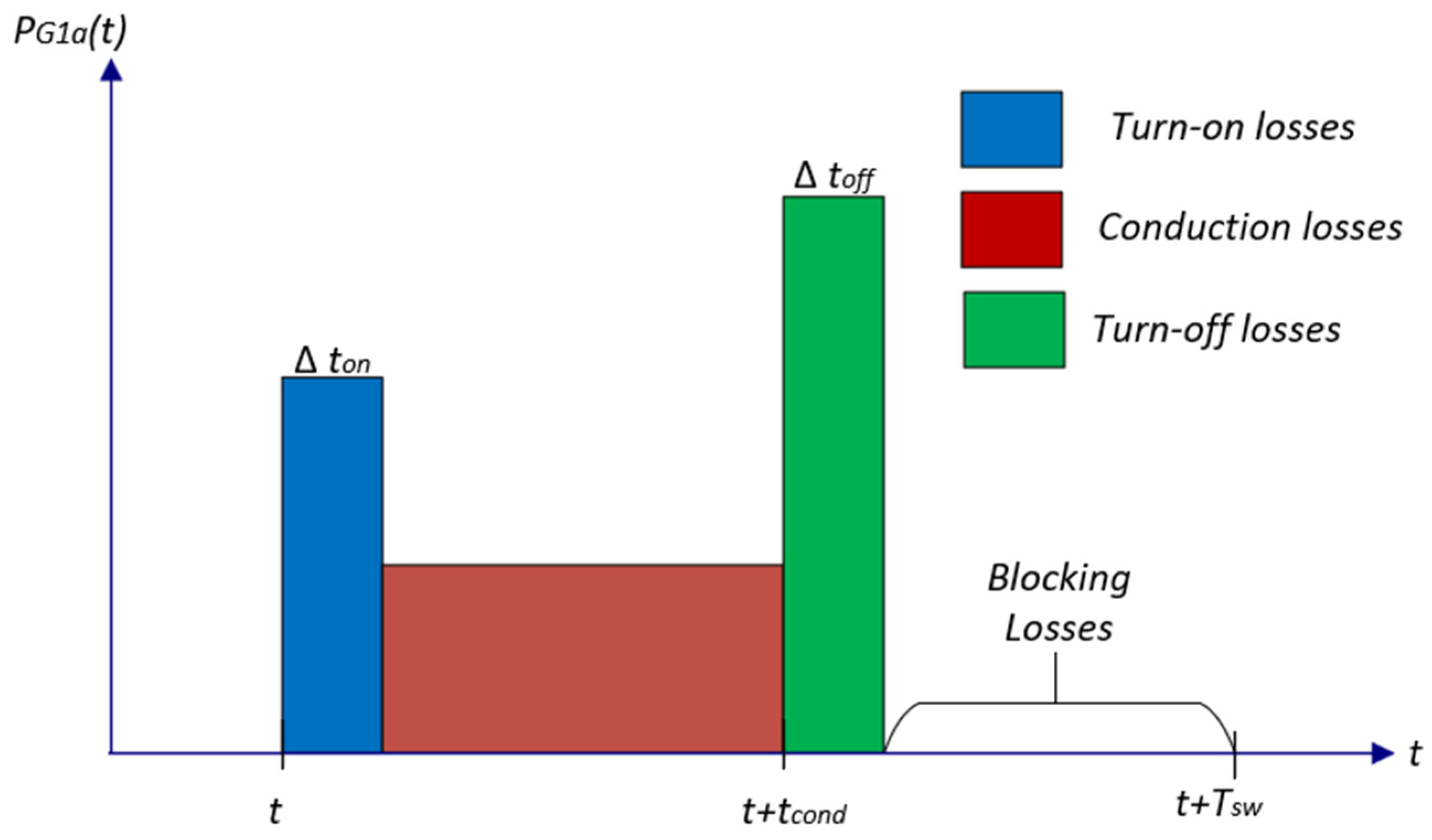
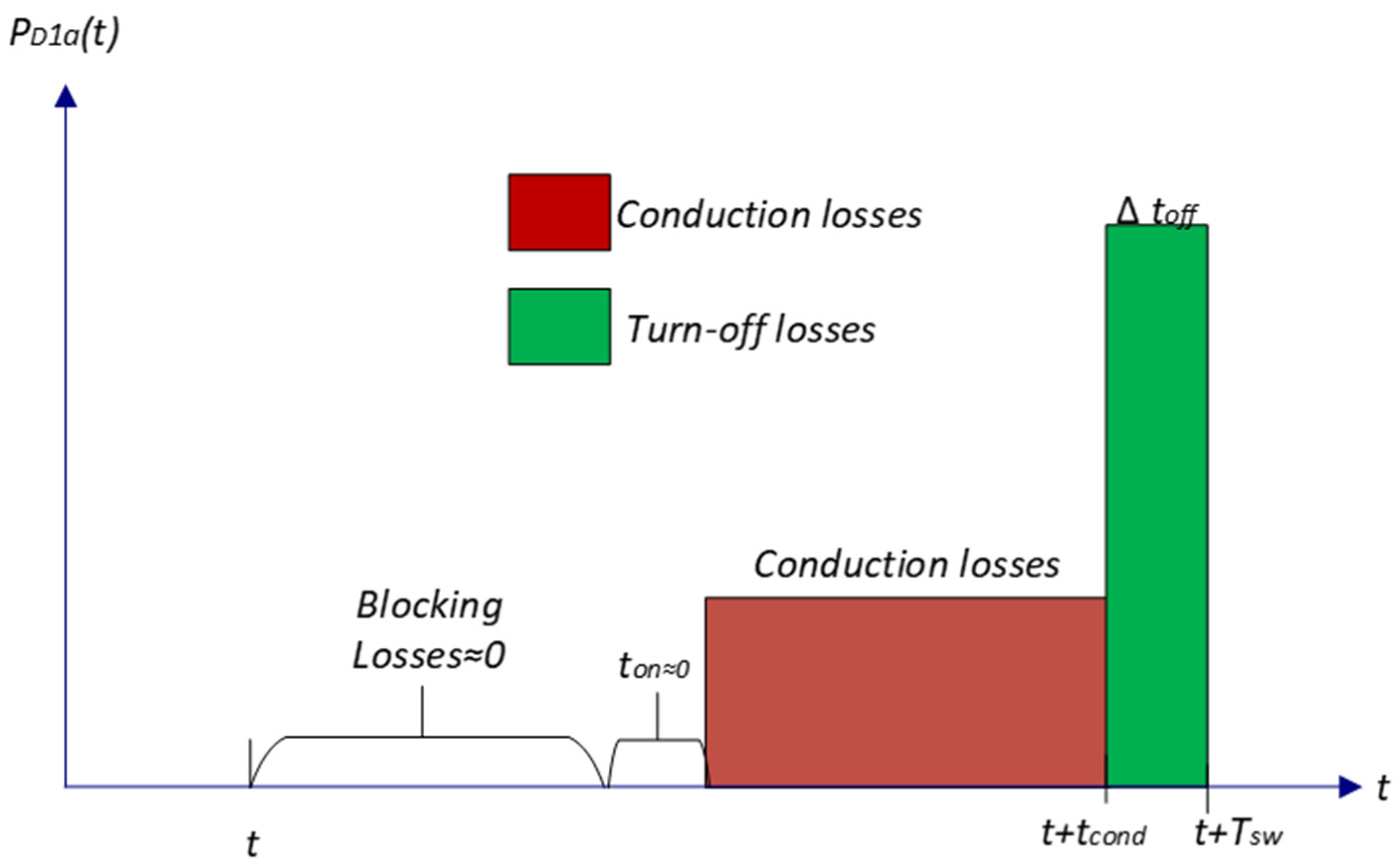
2. Bidirectional Switch Power Losses

The SPMCs are controlled utilizing a combination of power semiconductor devices, namely insulated gate bipolar transistors (IGBTs) and diodes, which operate as switching elements alternating between the conduction, blocking, and switching states in cyclical fashion. In each of these states, a power dissipation component is generated, resulting in heating of the semiconductor devices and contributing to the total power losses. The power dissipation of the devices is contingent upon the operating conditions of the converter (output frequency, switching frequency, modulation strategy, voltage and current operating levels, load characteristics, etc.). An analytical modeling approach for semiconductor losses in matrix converters is described and presented in [25]. The conduction and switching losses are modeled through simple mathematical expressions based on the ideal behavior of the device. The total average power losses over a fundamental period for any device has been formulated in [26] as:
P a v g = 1 T 0 T p t d t
where
  • p ( t ) is devices instantaneous dissipated power.
  • T is fundamental output current period.
The power dissipation of a semiconductor device at an arbitrary time instant t is equivalent to the mean conduction and switching losses incurred within the device over the switching period t + T s w subsequent to t [27], as illustrated in Figure 3. This methodology facilitates the derivation of simplified continuous time power loss expressions by approximating the instantaneous power losses as:
P t P c o n d   t + P s w   t = P c o n d   t + P o n   t + P o f f   t
where P c o n d   t and P s w t are the average conduction losses and average switching losses at each switching period, respectively. In this research, the UPS circuit schematic using SPMC topology is depicted in Figure 4. The power losses for IGBTs and diodes are enough to consider just one IGBT (for example S1a) and one diode (for example D1b) to calculate SPMCs’ power losses. In general operation of SPMCs for the positive cycle, the current flows through S1a and D1b and S4a and D4b, and for negative cycle, S2a and D2b and S3a and D3b. The total average power losses of IGBTs (S1a) can be expressed as follows:
P S 1 a t P c o n d / S 1 a   t + P s w / S 1 a   t = P c o n d / S 1 a   t + P o n / S 1 a   t + P o f f / S 1 a   t
The detail expression explanation has been described in [28] and Appendix D. Thus, the average power losses of the IGBT P S 1 a t can be calculated as below:
P S 1 a t = V S 1 a t I S 1 a t D S 1 a t + E o n / S 1 a t T s w + E o f f / S 1 a ( t ) T s w
P S 1 a t = V t S + a S I S 1 a b S I M   sin ω o t 1 2 1 + M sin ω o t + φ o + h I S 1 a k     ( t ) T s w + m I S 1 a n     ( t ) T s w
In the analysis of diode circuits, only two primary forms of power loss merit consideration: conduction losses and turn-off losses. The turn-on and blocking losses have been omitted from this analysis due to their negligible contribution to the total power dissipation described in [28,29] and Appendix D. A detail of the D 1 b schematic instantaneous dissipated power can be appreciated in Figure 5. Thus, the P D 1 b t can be described as below:
P D 1 b t P c o n d / D 1 b   t + P s w / D 1 b   t = P c o n d / D 1 b   t + P o f f / D 1 b   t
P c o n d D 1 b t = 1 T s w   t t + T s w V D 1 b t I D 1 b t d t = 1 T s w   t t + t c o n d / D 1 b + t o f f V D 1 b t I D 1 b t d t = V D 1 b t I D 1 b t D D ( t ) d t
Total power losses diode (D1b) can be expressed as below:
P D 1 b t   V D 1 b t I D 1 b t D D t + E o f f / D 1 b ( t ) T s w
As derived in details in Appendix D, then
P D 1 b t = V t / D + a D I D 1 b b D I M   sin ( ω o t ) 1 2 1 M sin ω o t + φ o + 0.5 I r r   0.5 V d c t b T s w
In this work, turn-on and turn-off energy losses has been calculated under certain test conditions as well as the modelling parameters of the IGBT and diode switching losses can be found in [27] and parameter on the data sheet for IGBT BUP314D and Diode IN4118. The parameters are depicted in Table 1, and the total losses for typical dan proposed UPS are depicted in Table 2 based on expressions (5) and (9).
In the context of the impact on the number of diodes and switches employed in the UPS system, Table 2 presents a comparative analysis of the devices and switches utilized in a typical UPS system and the proposed UPS system. The conventional UPS system necessitates 13 diodes and switch, comprising 8 diodes, 4 IGBTs, and a bypass switch to facilitate rectifier and inverter operations. Conversely, the proposed UPS system incorporates 4 bi-directional switches, encompassing 8 diodes and 8 IGBTs, which enable the system to execute both rectifier and inverter operations, while the proposed system has 18.75% more devices and switches than the conventional system. The total power losses for the proposed UPS are 455.6W, while those for the typical UPS are 289.8W. However, it retains the salient benefits of a compact system size, high power quality, low harmonic, and unity power factor. The proposed UPS notably, the paramount feature of the proposed novel advancement in single-phase UPS system design is the utilization of a singular circuit topology to perform both rectifier and inverter operations. Both operations can be controlled accordingly which cannot be done by the typical UPS system, in which the rectifier is based on uncontrolled operation. This attribute contributes to the realization of a high-power density power converter system, aligning with the power electronics technological roadmap, which aims to increase power density, efficiency dan reliability, and robustness.

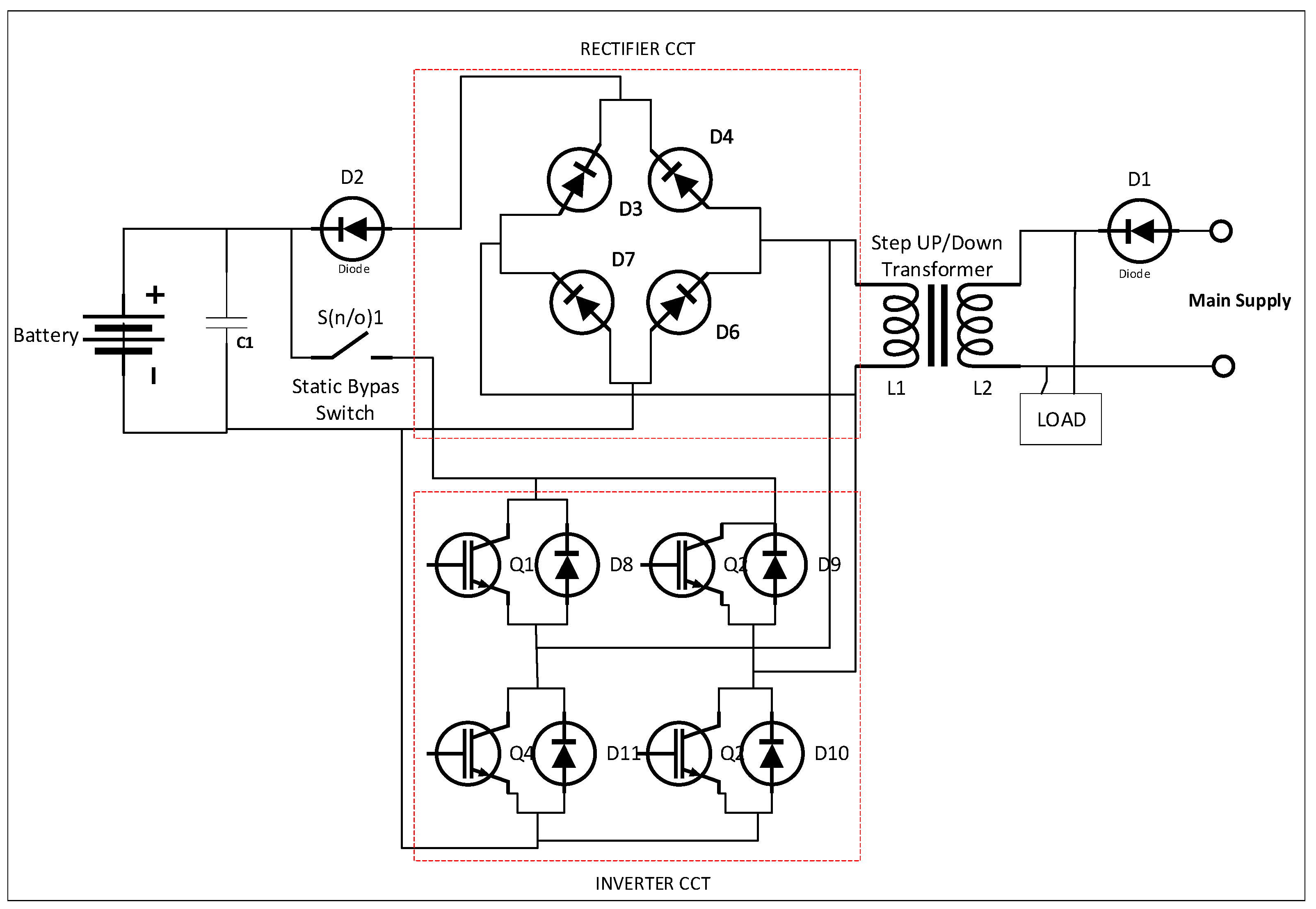
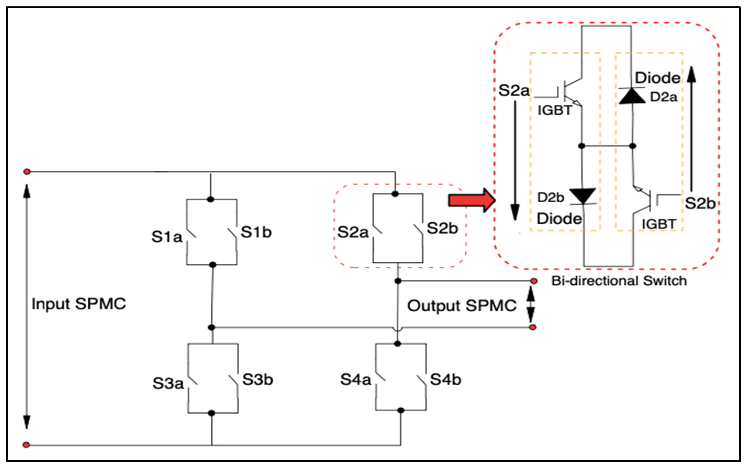
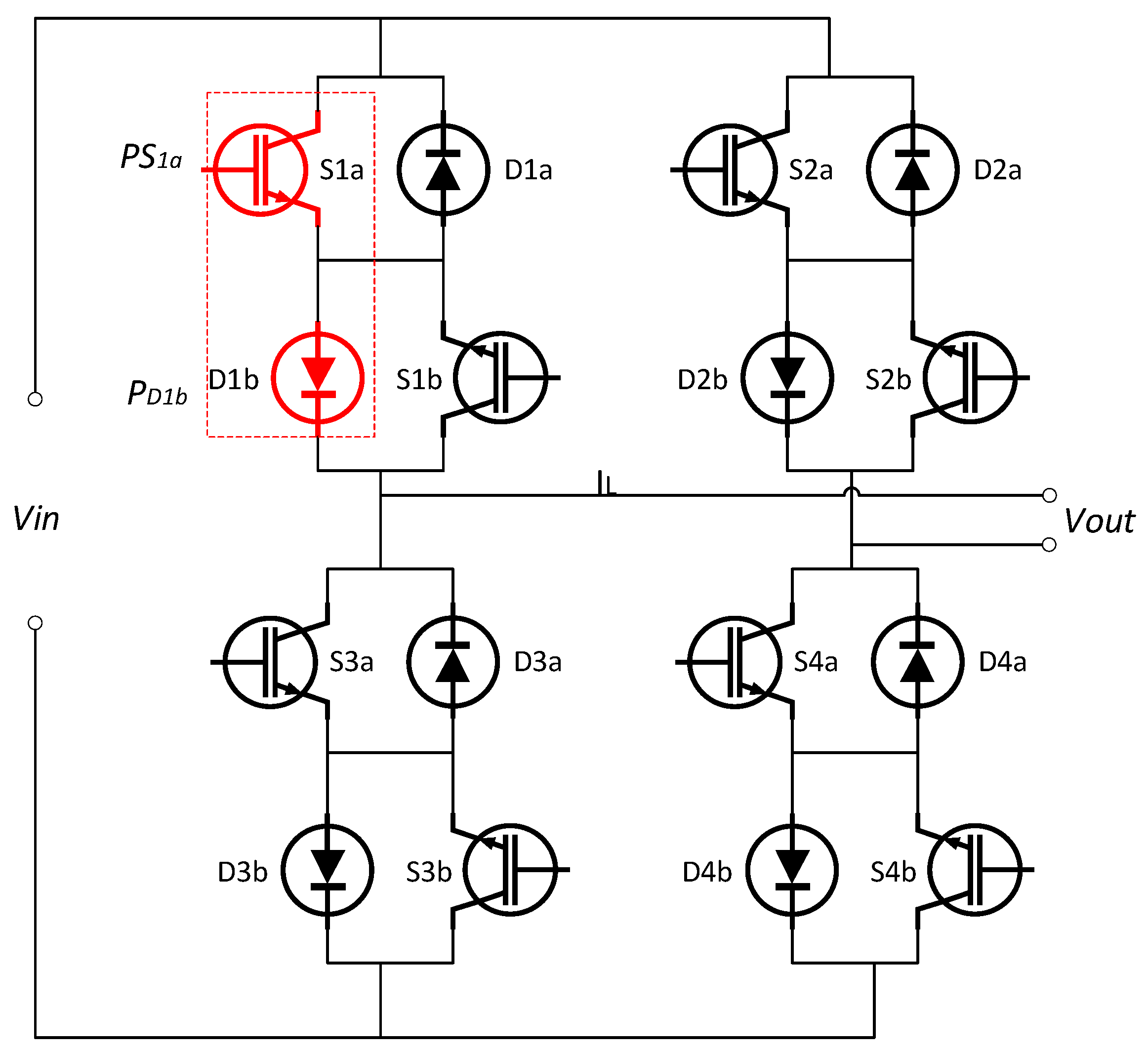
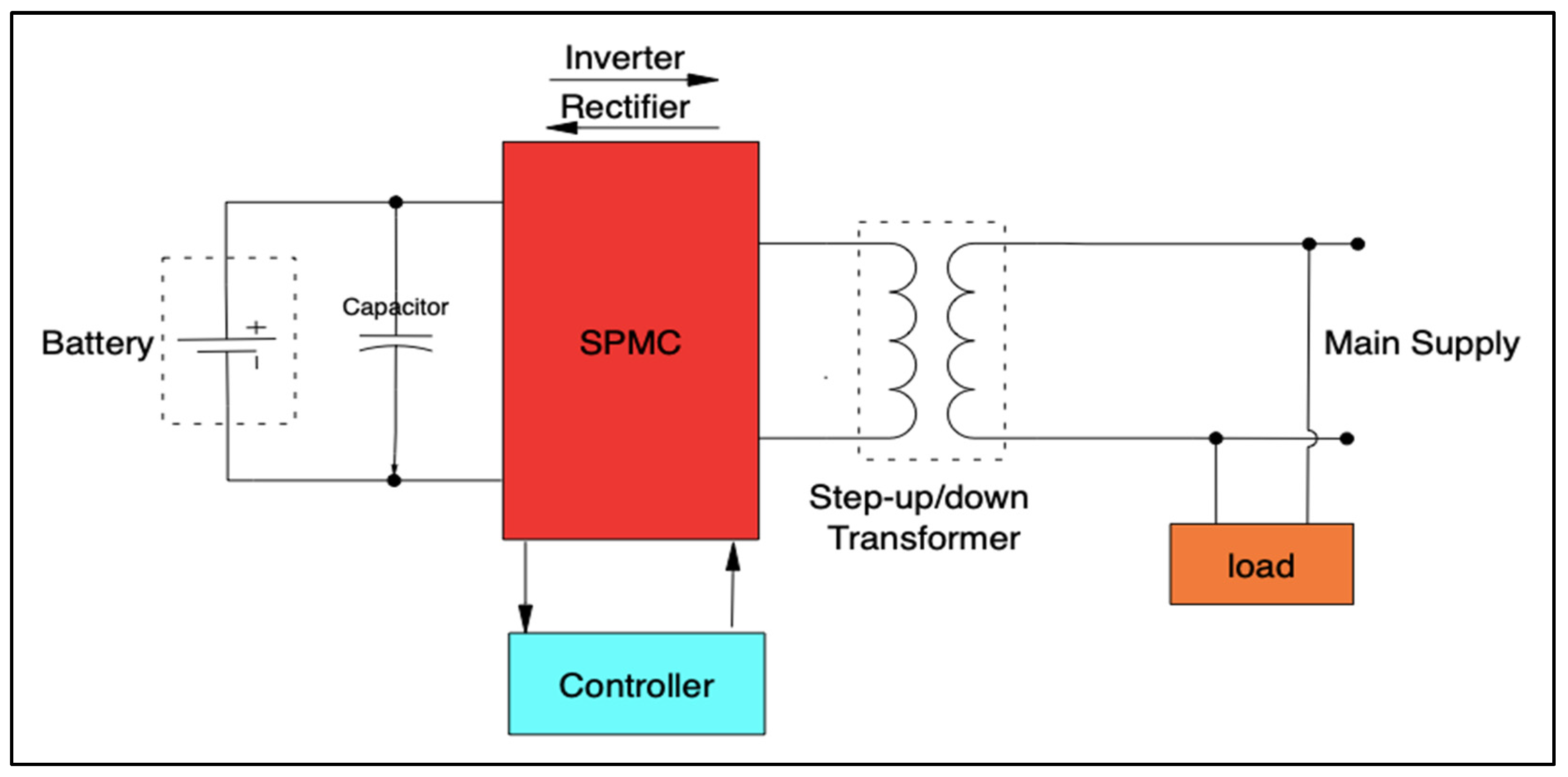
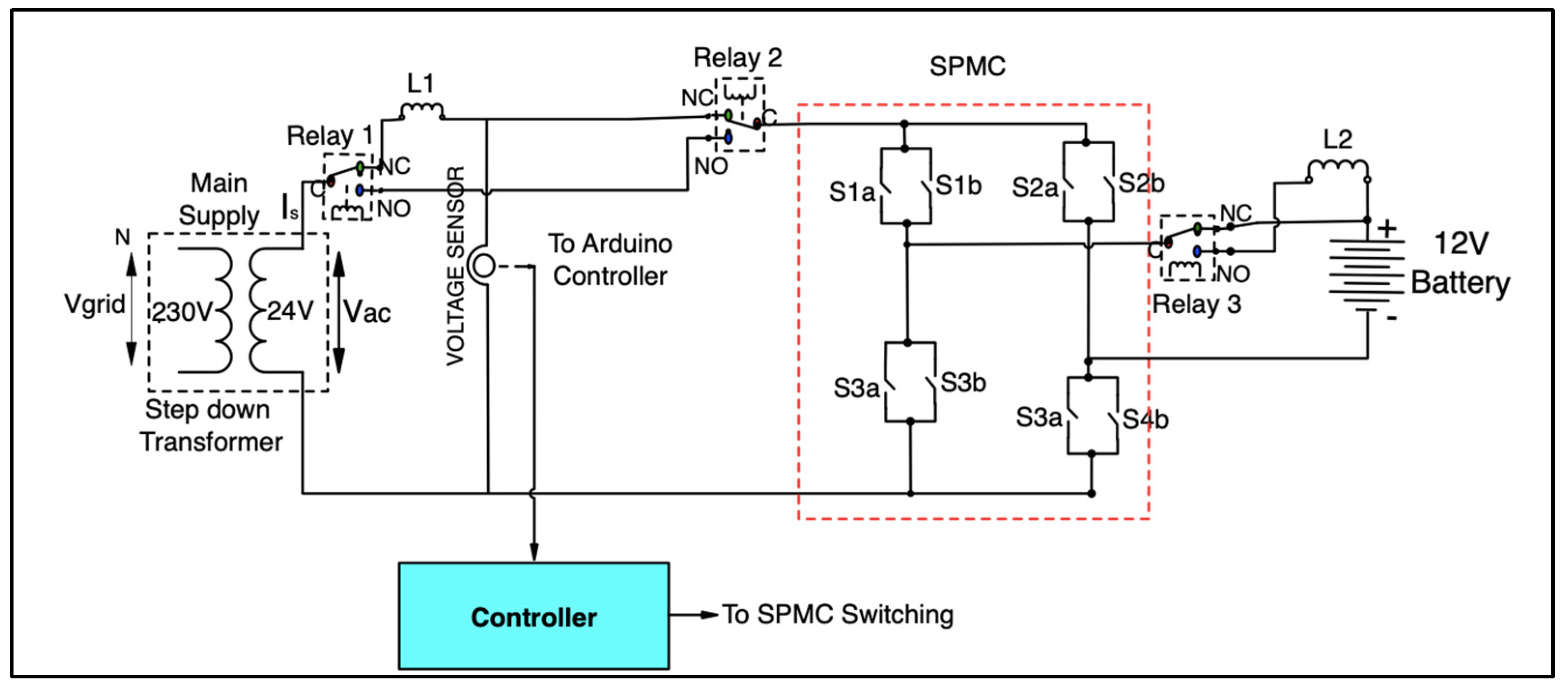
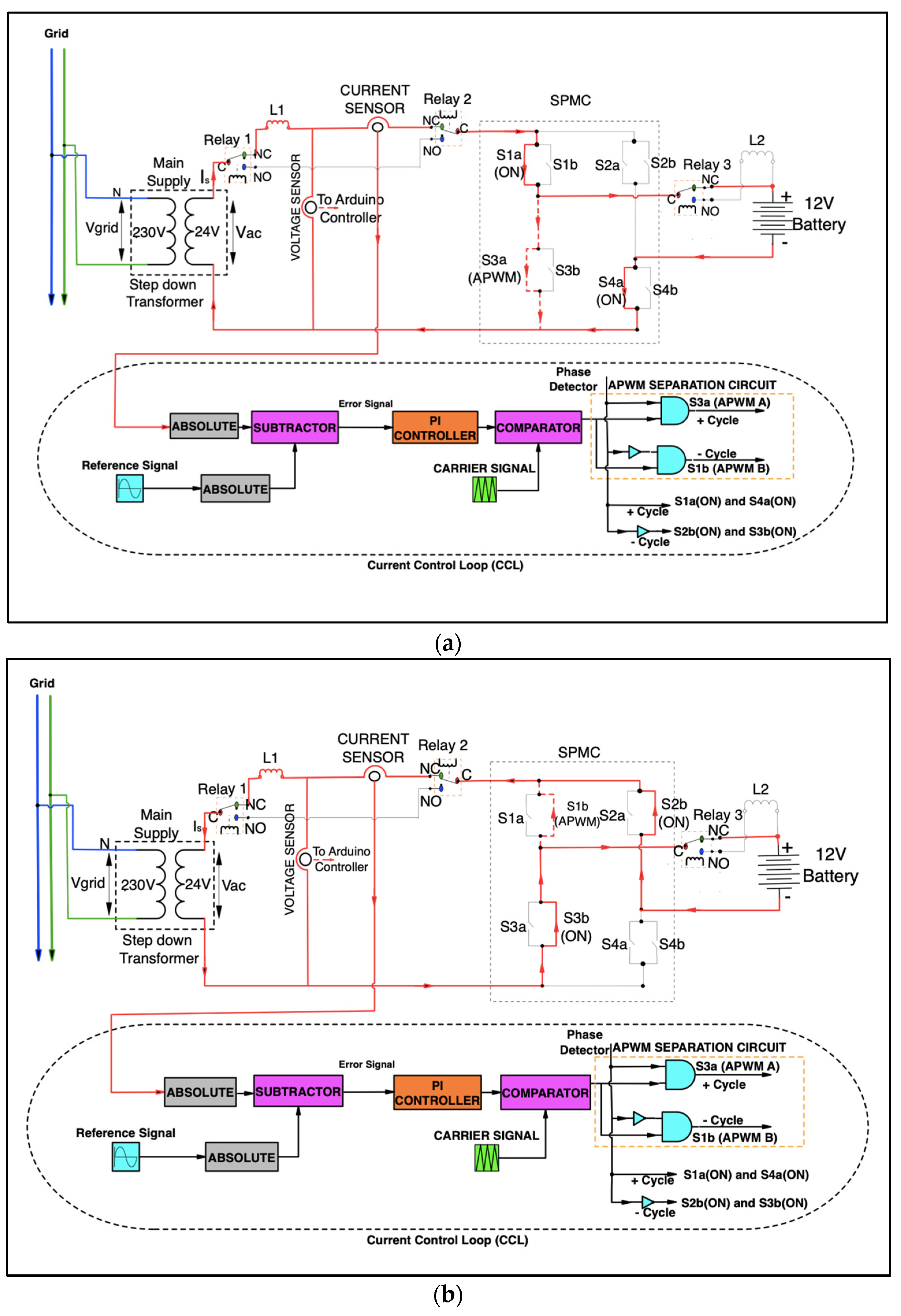
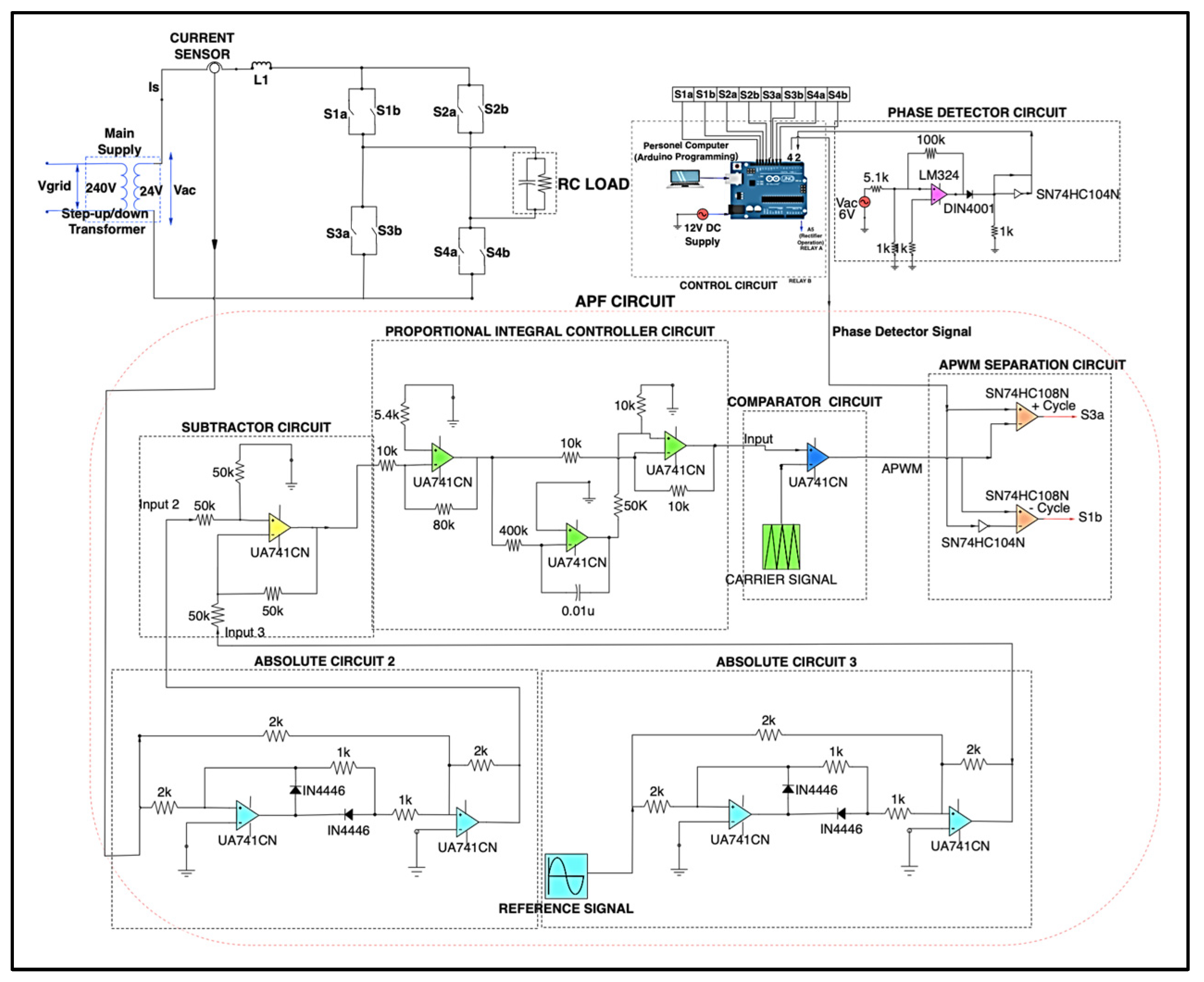
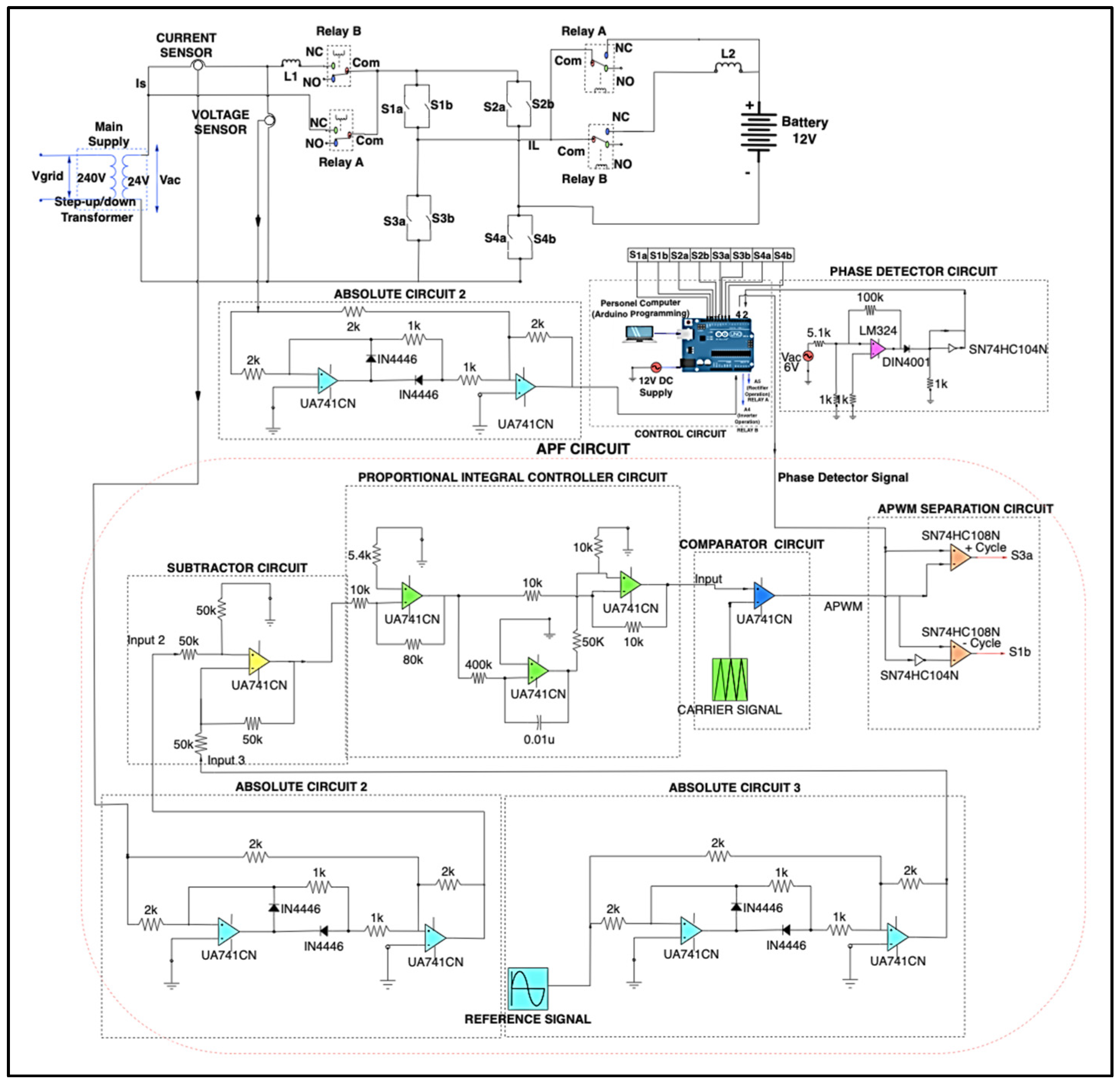
3. Topology of UPS System

The envisioned UPS architecture, utilizing the SPMC topology, is illustrated in Figure 6. This diagram, as previously noted, showcases a system solely comprising a single converter based on the SPMC topology, capable of functioning both as a controlled rectifier and a controlled inverter. The SPMC is strategically designed to switch roles between a rectifier (under standard conditions) and an inverter (during power disruptions), thereby obviating the necessity for distinct rectifier and inverter circuits found in conventional UPS designs. Figure 7 provides an intricate view of the circuit layout for the proposed rectifier and inverter configuration, notably absent of any filtering mechanisms. To facilitate its role in the UPS, a voltage sensor apparatus is employed to monitor the supply waveform within the circuit. This sensor plays a pivotal role in managing the transition between charging (rectifier mode) and discharging (inverter mode) operations within the UPS system.

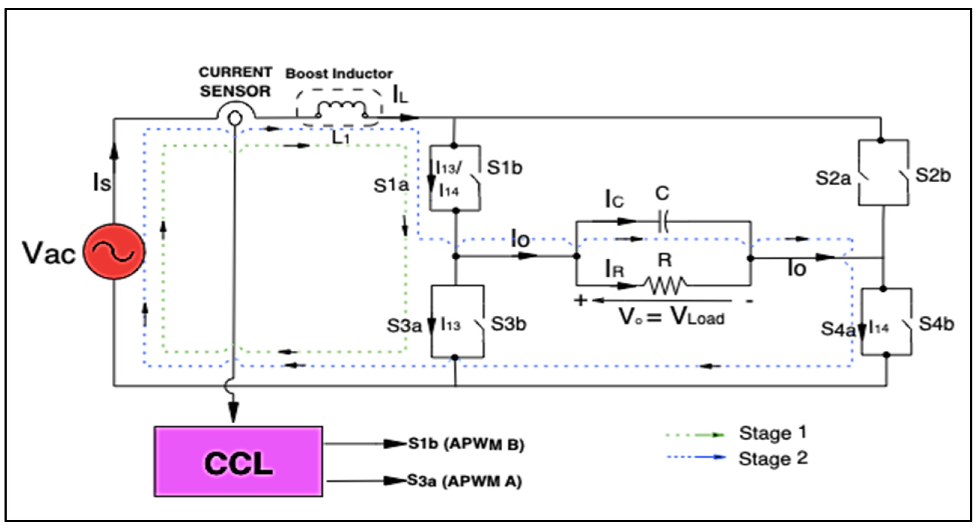
4. Topology of UPS System with APF Functionality

The enhancement of the UPS framework is achieved through the integration of SPMC topology alongside APF capabilities. The APF feature is specifically designed to mitigate harmonic distortions arising from non-linear load activities. In this research, the elimination of harmonic constituents from the non-sinusoidal supply current is facilitated through an innovatively designed APF, which leverages a current control loop (CCL) strategy employing a boost technique. This APF function effectively compensates the supply current, rendering it sinusoidal and synchronized with the supply voltage waveform, as depicted in Figure 8a and Figure 8b, respectively. To ensure system stability and enhance performance, the switching frequency for the controlled rectifier equipped with APF functionality was predetermined at 10 kHz, complemented by proportional and integral (PI) gains.
Figure 9 presents an intricate schematic of the circuit design for the rectifier function, enhanced with APF capabilities. To fulfill the requirements of the APF, an additional component, an inductor labeled L1, is incorporated to serve as the boost inductor. Furthermore, a current sensing device is deployed to monitor the supply current within the CCL framework. The CCL itself is composed of several key components: an absolute circuit, a subtraction circuit, a PI controller, and a comparator. This arrangement facilitates the generation of a sinusoidal reference signal, closely aligned with the supply waveform.

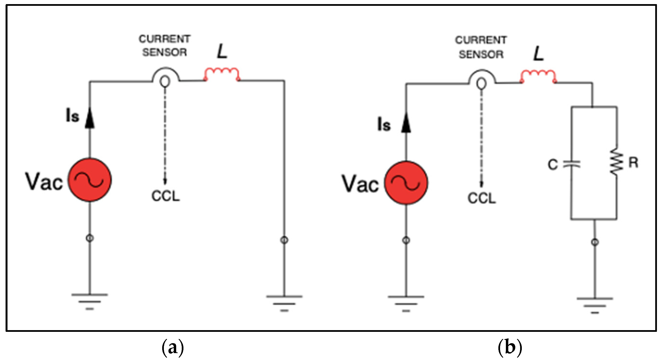
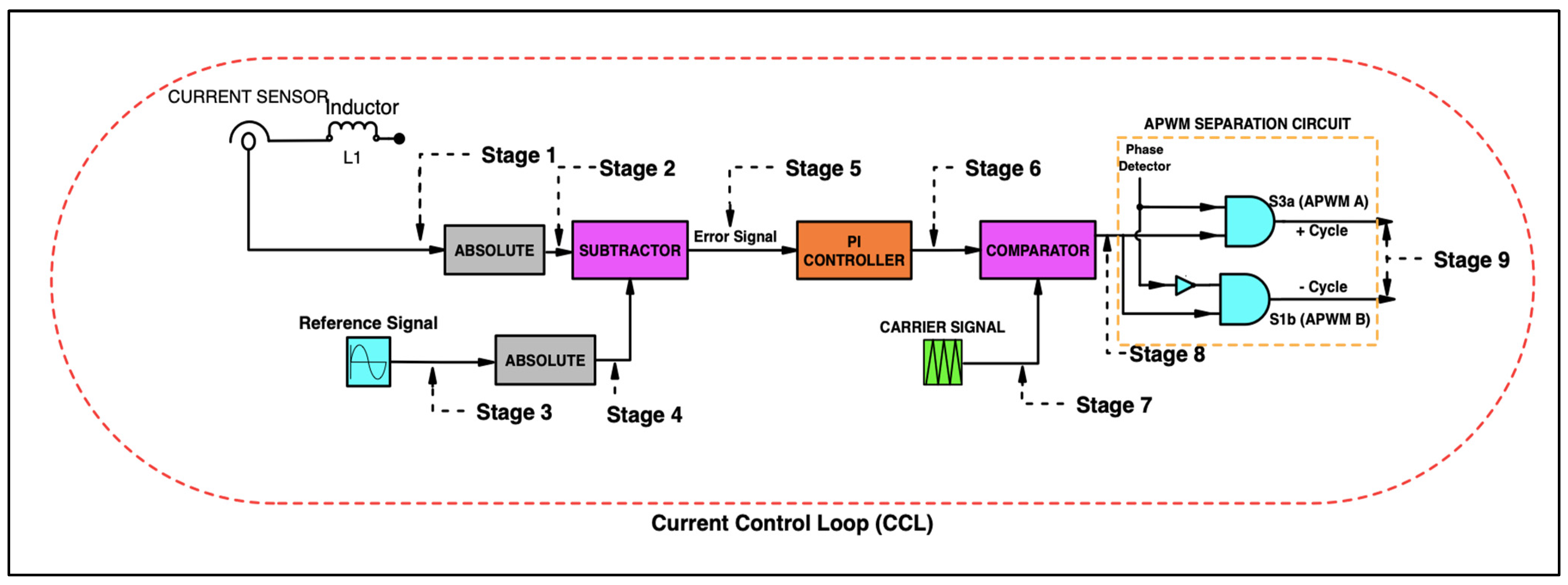
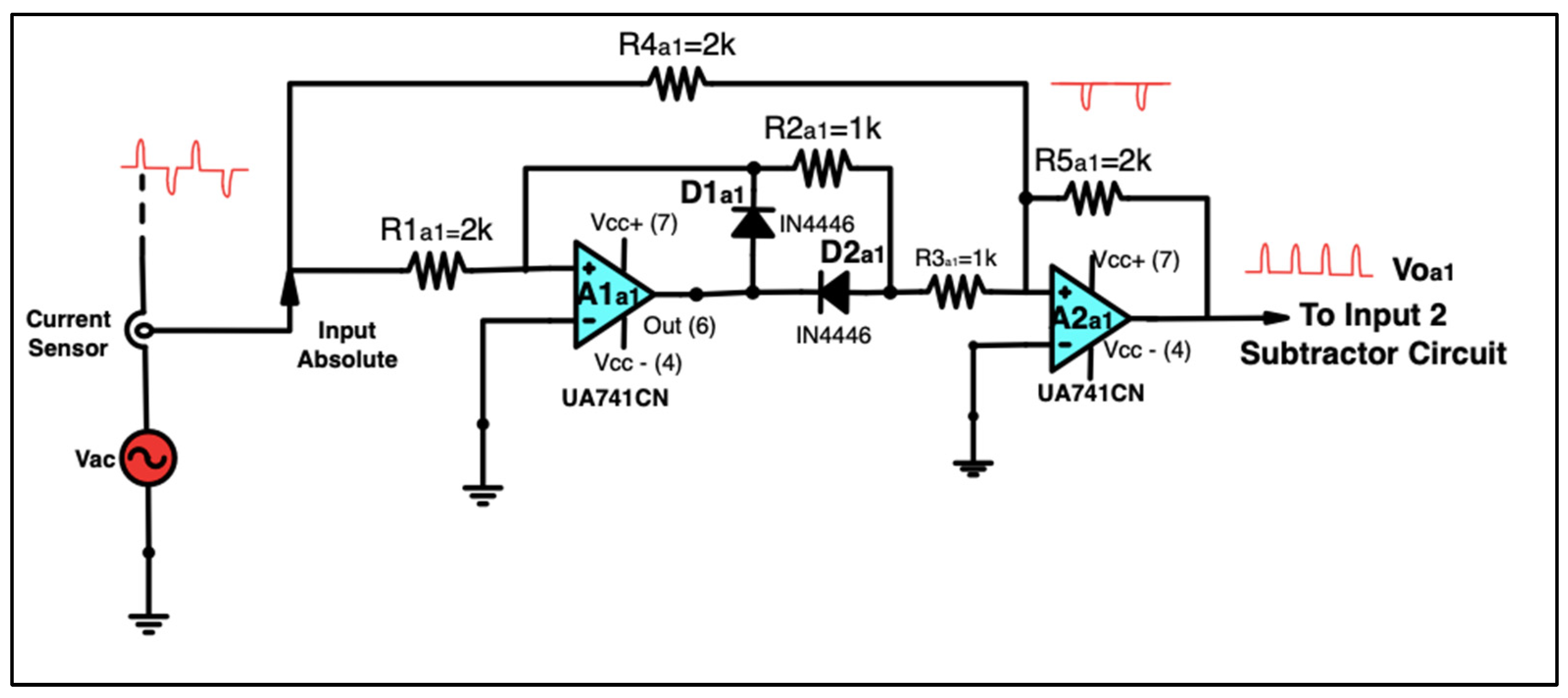
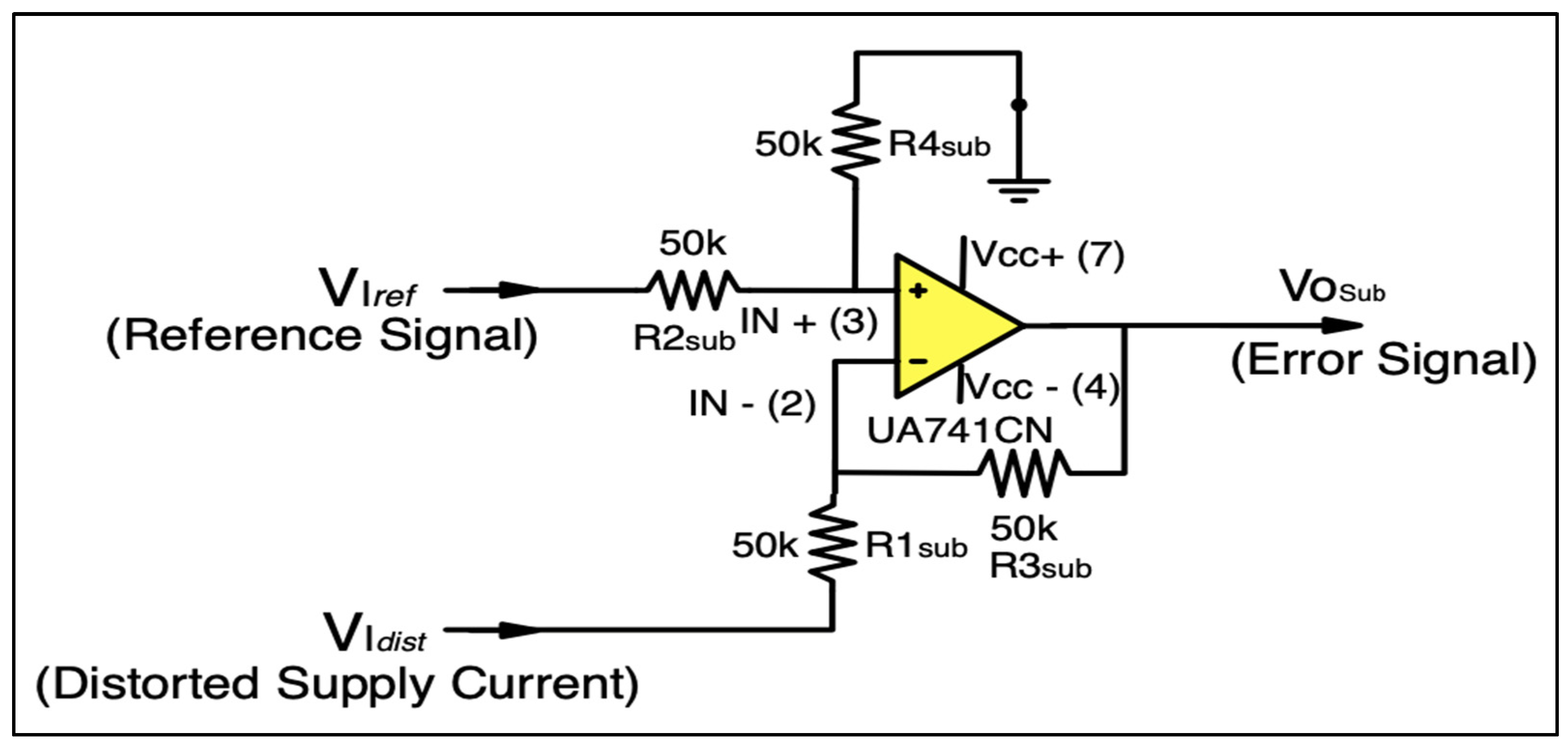
4.1. APF Mathematical Treatment Modeling

The mathematical treatment of the boost inductor is formulated based on Figure 10. The circuit operation can be divided into two stages. Stage 1 represents the circuit operation during the pair of switches S1a and S3a are turned ‘ON’. During this time, the current from the supply voltage flows through S1a and S3a and is defined as I13. Stage 2 represents the circuit operation during the pair of switches S1a and S4a are turned ‘ON’. At this time, the current from the AC supply flows through the pair of switches S1a and S4a and is defined as I14.
The inductor current is linearly ramped from I13 to I14 at stage 1, as shown in Figure 11. During this period, the boost inductor charges energy. The equation for this interval (defined directly as S 13 ) with relationship between voltage supply V a c and inductor voltage V L can be stated as:
V a c = V L
V a c = L I 14 I 13 S 13   or   L I S 13
Thus,
S 13 = I L V a c
Figure 12 shows the simplified circuit for the stage 2. During the pair of S1a and S4a are turned ‘ON’ ( S 14 ), and the energy from L1 is transferred to the load voltage V o . Therefore, the current of L1 decreases linearly during I14, and thus the supply current IS in this interval can be written as:
I s   = I L 1 = I 14
Meanwhile, voltage supply V a c is
V a c = V L + V o V a c = L I 13 I 14 S 14 + V o
or can be written as for stage 2:
V a c = L I S 14 + V o S 14 = I . L V o V a c
From Equations (13) and (14), both can be written as
I = V a c S 13 L = V o V a c S 14 L
From Equation (16), the boost inductor can be determined by
L = V a c S 13 I
Meanwhile, the slope of the ripple current waveform m, as shown Figure 13, is given by
m = 2 A T / 2 = 4 A T = 4 A f s
where A is the maximum permitted peak of ripple current and fs is the switching frequency. Otherwise, m also can be written as
m = I S 13
In this work, the maximum peak to peak ripple is 1% from the line current, which is 1.7 A. By rearranging Equations (18) and (19),
L = V a c S 13 I = V a c 4 A f s
Using the circuit parameters A is 0.085 A, fs is 10 kHz and Vac is 12 Vrms, the value of L can be determined as
L = 12 4 × 0.085 × 10 k = 4 mH
If the average capacitor current ic is same as the load current io and the capacitor supplies the energy to the load during S1a and S3a (S13) are turned ON, the peak-to-peak ripple voltage capacitor ∆Vc can be calculated as
V c = V c V c S 13 = 1 c 0 S 13 i c d t = 1 c 0 S 13 i o d t
The value of output voltage ripple for the load will be considerable during the line inductor energizing period and load capacitor discharging period. The output voltage ripple is given
d V l o a d V l o a d = δ T R C
where R is the load resistance, C is the capacitance, and δ is duty cycle ratio.
The mathematical treatment of APF is driven by the CCL to control the charging and discharging modes of operation of the boost inductor, as shown in Figure 14.
The Vac can be represented as:
V a c ( t ) = V a c sin ( ω t )
where ω is the angular frequency of the fundamental component. The summation of supply current Is with distortion components by using RC load can be written as
I s t = n = 1 I n s i n ( n ω t + θ n )  
where I n is amplitude of harmonic order n, and θ n is its phase. For implementation of APF in the system, Is can be written as
I s t = I 1 sin ω t + θ 1 +   n = 2 I n s i n ( n ω t + θ n )
The second part is the non-sinusoidal component and should be removed accordingly. The CCL is the crucial part of the rectifier operation to eliminate the non-sinusoidal component and to ensure that the supply current later becomes sinusoidal and in phase with V a c . To simplify the discussion of CCL, the circuit operation can be divided into nine stages, as shown in Figure 15.
At the initial phase, the current sensor detects the supply current IS, providing a crucial input to the CCL. This sensor is adept at identifying the waveform distortions in the supply current as previously discussed.
During the second phase, the bipolar distorted supply current waveform undergoes transformation into a unipolar waveform, courtesy of the absolute circuit. This conversion facilitates a forthcoming comparison with a unipolar carrier signal. The construction of the absolute circuit involves the utilization of two precision operational amplifiers (op-amps) and five precision resistors, as illustrated in Figure 16. In scenarios where the input signal exhibits a positive cycle, the output from op-amp A1a1 turns negative, causing diode D1a1 to exhibit reverse bias. Conversely, diode D2a1 enters a state of forward bias, effectively completing the feedback circuit around op-amp A1a1 via resistor R2a1 and establishing an inverting amplifier configuration. The op-amp A2a1 then aggregates the output from op-amp A1a1, applying a gain factor of −2, alongside the input signal which is subject to a gain factor of −1, resulting in an overall gain of +1. When the input signal is in its negative cycle, diode D1a1 assumes a forward bias, enabling the feedback loop around op-amp A1a1, while diode D2a1, being reverse-biased, remains non-conductive. Consequently, op-amp A2a1 inverts the input signal, yielding a positive output voltage that encapsulates the absolute magnitude of the supply current, irrespective of whether it is in its positive or negative state.
Let us consider the case with R2a1 = R3a1 = R and R1a1 = R4a1 = R5a1 = 2R. The circuit operation is divided into two intervals. During interval 1 (positive half-cycle), Vac is positive, and V1amp1 = −Vac. The voltage at the output V0a1 of op-amp A2a1 can be found from:
V 0 a 1 = R 3 a 1 R 2 a 1 V 1 a m p 1 + R 3 a 1 R 4 a 1 V a c
V 0 a 1 becomes
V 0 a 1 = 1 V 1 a m p 1 0.5 V a c = V a c 0.5 V a c = V a c for   V a c 0
During interval 2 (negative half-cycle), Vac is negative, and V2amp2 = 0. Thus, by using Equation (26) again and if R3a1 = R4a1 = 2R and R2a1 = R, V0a1 of op-amp A2a1 is:
V 0 a 1 = 1 V 1 a m p 1 0.5 V a c = 2 0 V a c = V a c for   V a c < 0
Next, stage 3 presents the input reference signal for the CCL. The AC supply is used as a reference signal represented as reference current Iref. The magnitude of Iref is determined based on the peak amplitude of the distorted supply current waveform, which is derived from the rectifier’s operation devoid of any filtering mechanism.
Stage 4 performs similarly to stage 2, in which the bipolar form of the reference signal is converted to the unipolar form. The output from the operational amplifier is a positive voltage indicative of the absolute magnitude of the input reference signal, regardless of its initial positive or negative value.
In stage 5, the output of the subtractor circuit is presented as shown in Figure 17. The subtractor circuit is used to subtract the sensed supply current (distorted current) Idist with Iref, in order to produce an error signal. This error signal needs to be eliminated for improving the supply current to be without distortion.
The effect of subtraction can be seen from the following qualitative observations. If VIdist = 0, then R1sub becomes grounded and Vp is proportional VIref, and so we have a non-inverting amplifier with Vosub proportional to V 2 s u b . However, if VIref = 0, then Vp = 0, and so we have an inverting amplifier with V o s u b proportional to –V1sub. Thus, in general we expect the output to be different voltage.
For a quantitative analysis, the op-amp is assumed to be ideal and note that R2sub and R3sub form a voltage divider such that
V P = R 3 s u b V 2 s u b R 2 s u b + R 3 s u b
Then, since an ideal op-amp has
Vin ( 2 ) = Vin ( 3 ) = Vp and in = 0 , i 3 = i 1 = V I d i s t V i n ( 2 ) R 1 s u b = R 3 s u b R 2 s u b + R 3 s u b V I r e f R 1 s u b V I d i s t R 1 s u b
Therefore,
V o s u b = V i n ( 2 ) + R 3 s u b i 3 = R 3 s u b R 2 s u b + R 3 s u b V 2 s u b + R 3 s u b R 2 s u b + R 3 s u b R 3 s u b R 1 s u b V 2 s u b R 3 s u b R 1 s u b V I d i s t = R 3 s u b R 1 s u b 1 + R 1 s u b R 3 s u b 1 + R 2 s u b R 3 s u b V I r e f R 3 s u b R 1 s u b V 1 s u b
Finally, if R 2 s u b R 3 s u b = R 1 s u b R 3 s u b , then
V o s u b = R 3 s u b R 1 s u b V 2 s u b V 1 s u b
Stage 6 presents the PI controller, as shown in Figure 18. With a proper tuning of proportional gain Kp and the integral gain Ki, the error signal as discussed in stage 5 can be eliminated. For this purpose, the two variable resistors Rp and Ri are used to vary the amplitude of the error signal. First, Rp is set to 80 k Ω to get Kp of 8. Then, Ri is set to 400 k Ω to get Ki of 27. The error from the output of the subtractor circuit is the input to the proportional controller.
Meanwhile, two important notes must be taken. First, the output of proportional controller is inverted. Also, it has no offset. The input to the integral controller is the output of the proportional controller, or is defined as below:
V i n p i = K p V e r r o r
With initial condition of Voi, the output of the integral controller is
V o i = 1 R i C i V i n p i d t + V o p = K i V i n p i d t + V o p
Substituting V i n p i = K p V e r r o r into Equation (34) gives
V o i = K i K p V e r r o r d t + V o p V o i = K p K i V e r r o r d t + V o p
The summer is actually a different amplifier, or can be defined as below:
V o s u m = 10 k 10 k K p K i V e r r o r d t + V o p K p V e r r o r V o s u m = K p V e r r o r + K p K i V e r r o r d t + V o p
The Laplace transform of Equation (34) is
V o s u m = K p V e r r o r + K p K i s V e r r o r
By rearranging it,
V o s u m V e r r o r = K p s + K i s = K p T i s + 1 T i s
where
T i = 1 K i = R i C i
If Ri = 400 kΩ and Ci = 0.09 µF,
K i = 1 R i C i = 1 400 k 0.09 μ = 27
Stage 7 represents the triangular carrier signal. The 10 kHz triangular carrier signal is used to represent the switching frequency of the APF.
In stage 8, the comparator circuit is used to generate the asynchronous PWM (APWM) signal by comparing the triangular carrier signal with the output signal of the PI controller. This APWM signal is used to control switches S3a and S1b for charging and discharging of boost inductor to perform the APF function.
Finally, in stage 9, the APWM separation circuit is developed for positive and negative cycle operations, by using two gates, an AND gate and an inverter gate. The separation is performed by comparing the generated APWM signal with the phase detector signal. The positive cycle is used to control S3a, while the negative the cycle is used to control S1b.
As mentioned in Section 1, the preliminary assessment was performed on the previous switching strategy in [23]. The switching strategy was implemented in the experimental work. However, the initial findings showed the output voltage of inverter operation was lower than expected with only 8 V. The designed target should be to producing at least 24 V in order for it to be possible to step the voltage up to 230 V using the step-up transformer connected to the grid. In addition, the boost inverter was used to boost output voltage, which, however, could only rise to 12 V. Therefore, further improvement to the switching algorithm is proposed, as detailed in the next subsections. The next subsections will explain the operation of the proposed UPS system in two designed modes: controlled rectifier (charging mode) and controlled inverter (discharging mode).

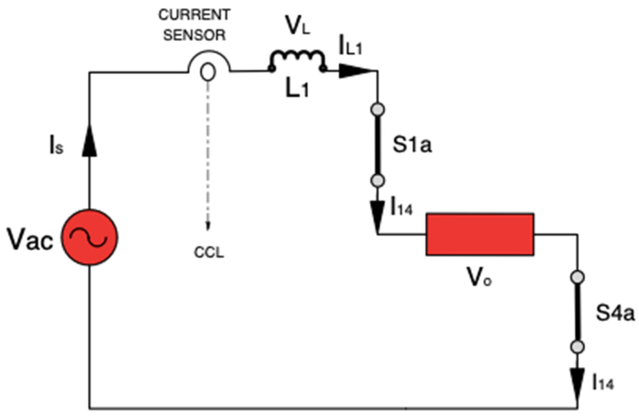
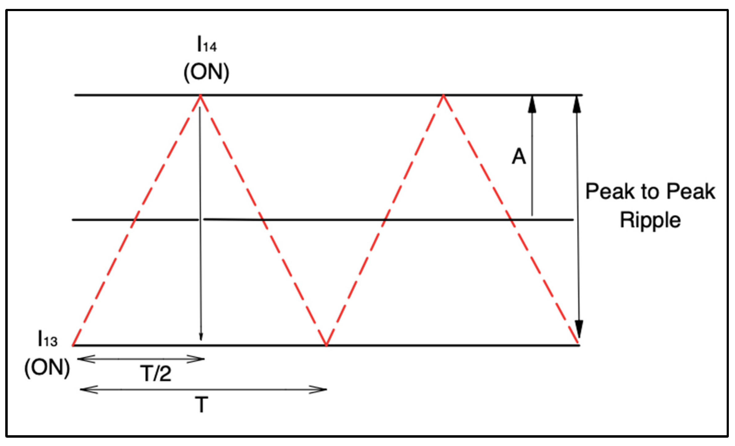
4.2. Controlled Rectifier Mode (Charging Mode)

The function of the controlled rectifier mode, also known as the charging mode, is to facilitate the conversion of AC from the grid to the DC required by the load [24,30]. This conversion process, when integrated with APF capabilities, involves two distinct operational phases: the positive and negative cycles. The APF’s role is pivotal in enhancing the quality of the supply current waveform, transforming it into a continuous, sinusoidal form that is synchronized with the supply voltage waveform. This adjustment significantly diminishes the THD and augments the power factor. Figure 19 elucidates the comprehensive mechanism of the controlled rectifier mode, whereas Table 3 details the specific switching strategy employed for both the positive and negative cycles. An in-depth exploration of each cycle’s operation is provided below.
  • Step 1 (Positive Cycle):
During the positive cycle, the inductor L1 initiates energy accumulation as switches S1a and S3a remain activated and turned ON. S3a’s operation is modulated by the APWM signal emanating from the CCL.
  • Step 2 (Positive Cycle):
Subsequently, as L1 transitions to the de-energization phase, the previously accumulated energy is relayed to capacitor C1, with switches S1a and S4a maintaining their active turned ON states to ensure a continuous flow of supply current.
  • Step 3 (Negative Cycle):
Conversely, in the negative cycle, the energization of L1 commences with the activation of switches S3b turned ON and S1b APWM Signal. The flow of supply current through S1b is governed by the APWM signal from the CCL. In this mode of operation, the line inductor (L1) starts charging the energy base on the APWM pulse signal when the pair of switches S3b and S1b are turned ON.
  • Step 4 (Negative Cycle):
In this negative cycle, consistently activated S3b turned ON, leads to the subsequent de-energization phase of L1. During this phase, the energy stored is dispensed to the resistive-capacitive (RC) load, facilitated by the continuous activation of switches S3b and S2b. The graphical representation of the waveforms pertaining to the charging mode is depicted in Figure 23, with the mode’s operation spanning from 0 to 40 ms.

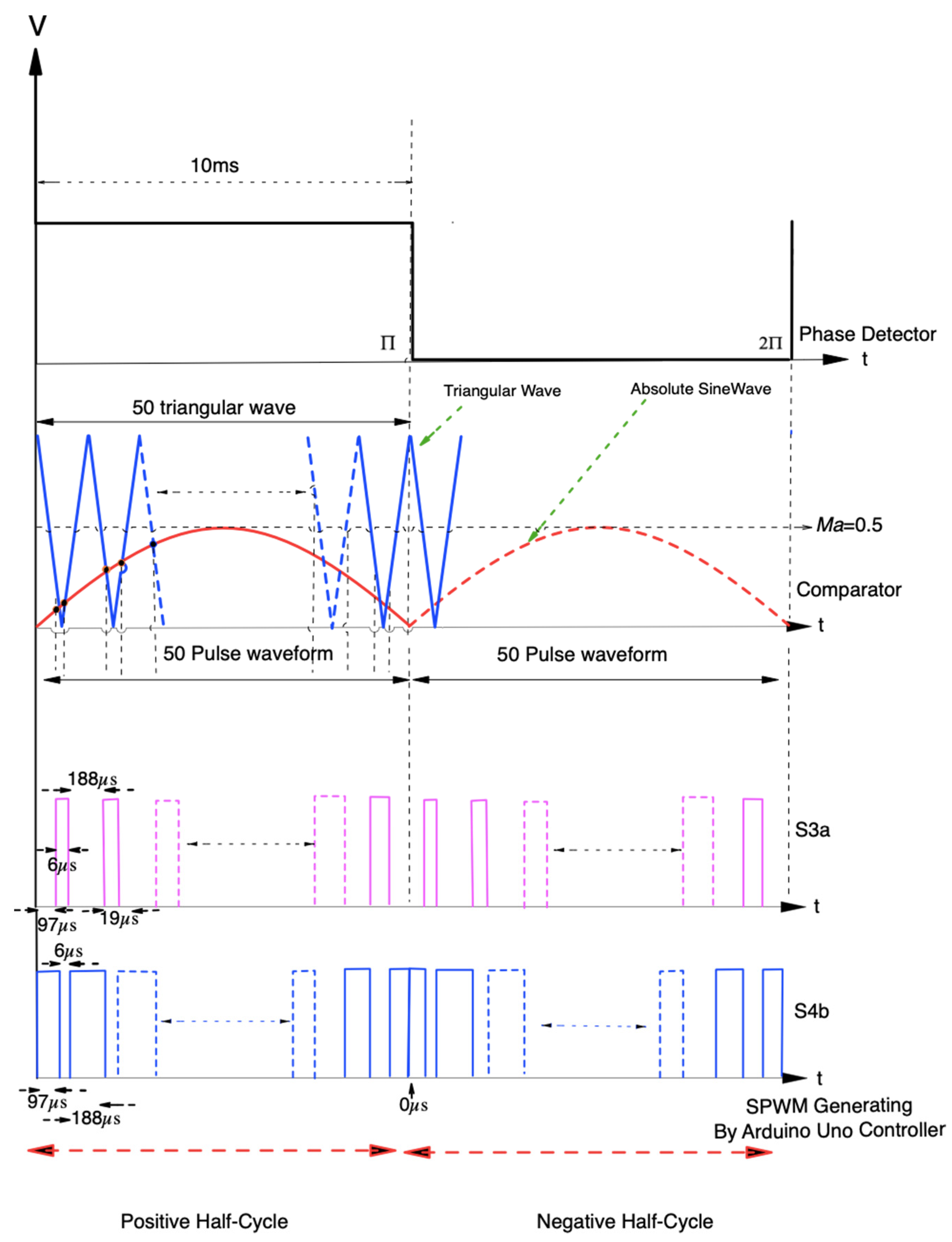
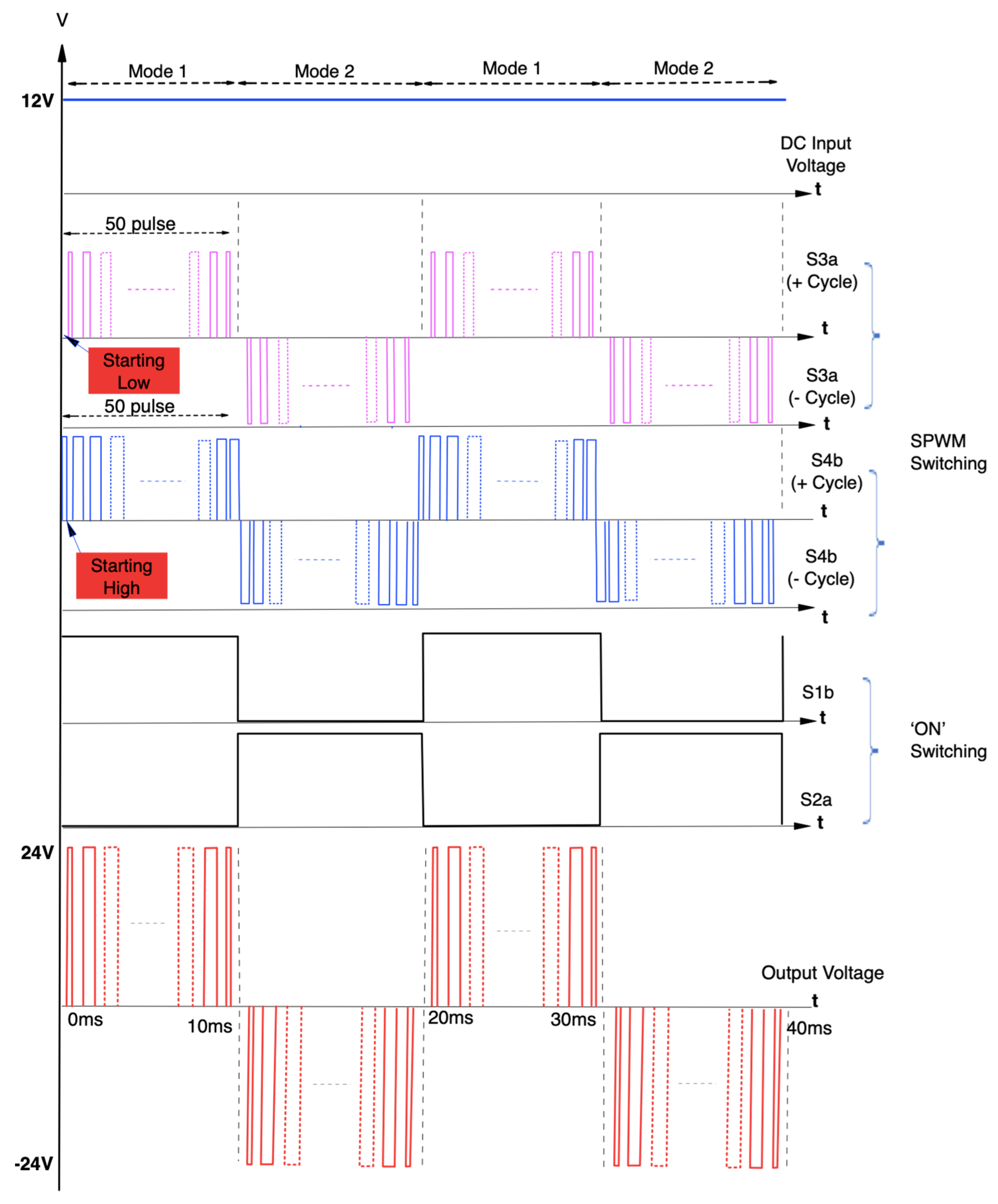
4.3. Managed Inverter Phase (Energy Release Mode)

The functionality of the managed inverter phase (energy release mode) pertains to the transformation of DC to AC, facilitating the conversion of DC energy from a backup source into the AC format necessary for the load [22,30]. Utilizing a boost inverter for the DC to AC conversion process, this mode produces an AC output voltage that exceeds the initial DC input; this elevation in output voltage is achieved through the modulation index of SPWMs. The switching frequency of 5 kHz will generate signals of 50 pulses for half a cycle and 100 pulses for one full cycle. Therefore, to generate the SPWM signal by using the Arduino Uno controller, the time of the pulse signals is required. Thus, the sampling time for the half-cycle of the 5 kHz SPWM signal is captured from MATLAB/Simulink. The details of sampling time for the 5-kHz SPWM signal with the modulation index of 0.5 are presented in Appendix A. The Switching frequency is set to 5 kHz for experimental dan simulation test base on the previous work published in [31].
The input voltage of 12 V from a battery incorporated with a boost inductor of 2 mH is used to develop an output AC voltage of 24 V. The voltage level is enough to send it back to the grid via a 24/230 V step up transformer. During power outage condition, the voltage sensor senses the value of the supply voltage level as zero. The UPS operation automatically changed from charging mode to discharging mode. As previously highlighted, a switching strategy was devised to guarantee the generation of a minimum output voltage of 24 V, facilitating the amplification of voltage to 230 V via a step-up transformer for grid integration. This aspect of the research has been meticulously focused on the switching technique within the managed inverter phase, ensuring its practical applicability for experimental validation on a test rig.
Figure 20 delineates the comprehensive mechanism of the managed inverter phase, incorporating a safe-commutation feature alongside innovative switching strategies for both the positive and negative cycles. Concurrently, Table 4 outlines the specified switching strategy and pulse signals designated for each cycle. An expanded explanation for the operational dynamics of each cycle is provided.
  • Positive cycle:
Step 1: For the positive cycle operation, the Arduino Uno controller generates the 1st to 50th pulses of the SPWM signal. As shown in Figure 21, for S3a, the 1st pulse is generated after a delay time (OFF state) of 97 μs, then the ON state of 6 μs, before it turns to the OFF state for 188 μs. The process is continuous until the Arduino Uno controller generates the 50th pulse as illustrated in Figure 22. Figure 22 illustrates generation of the SPWM signal using the Arduino Uno controller based on the sampling time as tabulated in Appendix A.
For S4b, the 1st pulse is generated to be the ON state of 97 μs, then the OFF state of 6 μs, before it turns to the ON state for 188μs. The process is continuous until the Arduino Uno controller generates the 50th pulse as illustrated in Figure 22.
Step 2: Energy is stored in the boost inductor as current flows from the 12V battery supply through the combination of switches S3a and S4b.
Step 3: Subsequently, the energy previously accumulated is conveyed to the load via the switch pair S1b and S4b, marking the transition of DC power to the AC load during the positive half-cycle of the boost inverter operation. To facilitate this process, switch S1b is activated to the ‘ON’ position, whereas switches S3a and S4b are modulated by the SPWM signal, employing a modulation index set at 0.5.
  • Negative cycle:
Step 1: For the negative cycle operation, the Arduino Uno controller generates the 51st to 100th pulses. The generation of SPWM signal for this cycle is also shown Figure 18 and Appendix A. For S3a, the 51st pulse is generated after a delay time (OFF state) of 199 μs, then the ON state of 2 μs, before it turns to the OFF state for 197 μs. The process is continuous until the 100th pulse as also illustrated in Figure 22.
For S4b, the 51st pulse in this cycle is generated to be ON state of 199 μs, then the OFF state of 2 μs, before turning to the ON state for 197 μs. The process is continuous until the the 100th pulse is generated.
Step 2: The configuration of the SPWM is designated as step 1, wherein switch S1b is deactivated, and the duo of S3a and S4b remains under the regulation of the SPWM, also in accordance with step 1. During this phase, the initiation of the SPWM signal is characterized by a high pulse pattern, specifically tailored for the negative half-cycle.
Step 3: During this phase, current is drawn from the 12V battery supply and directed towards the AC load via S3a, then returns through S2a. Consequently, this facilitates the conversion of DC power to the AC load, executing the boost function of the inverter throughout the negative half-cycle.
The waveforms of the discharging mode are shown in Figure 23, operating after the charging mode. The period assigned for this mode is from 40 to 80 ms.

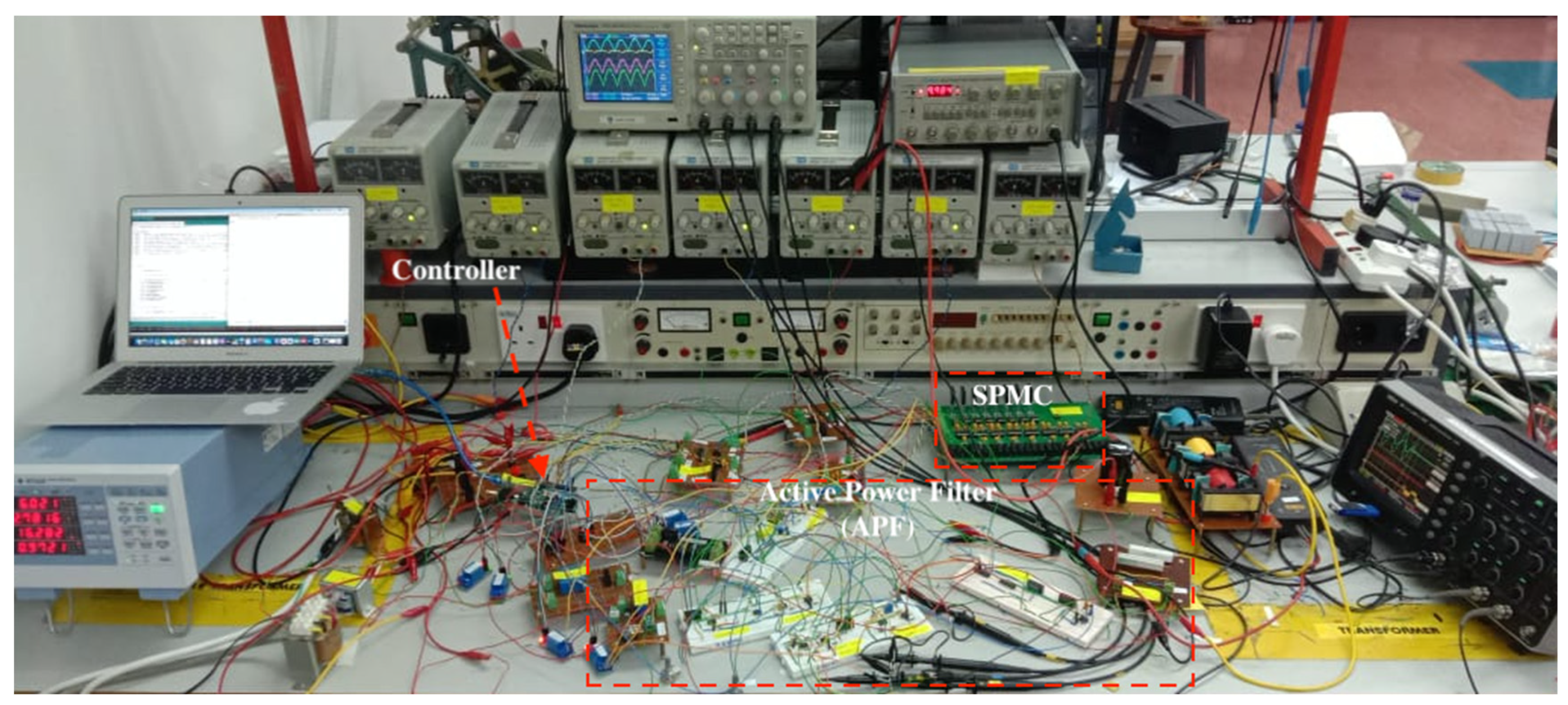
5. Simulation Model and Experimental Test Rig
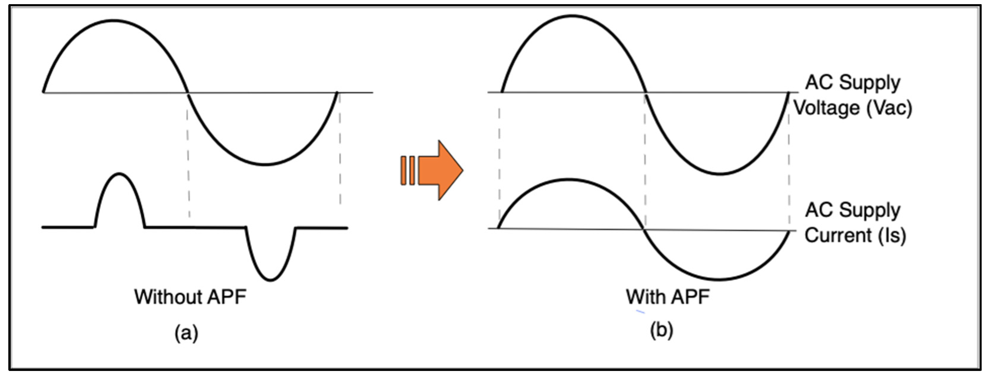
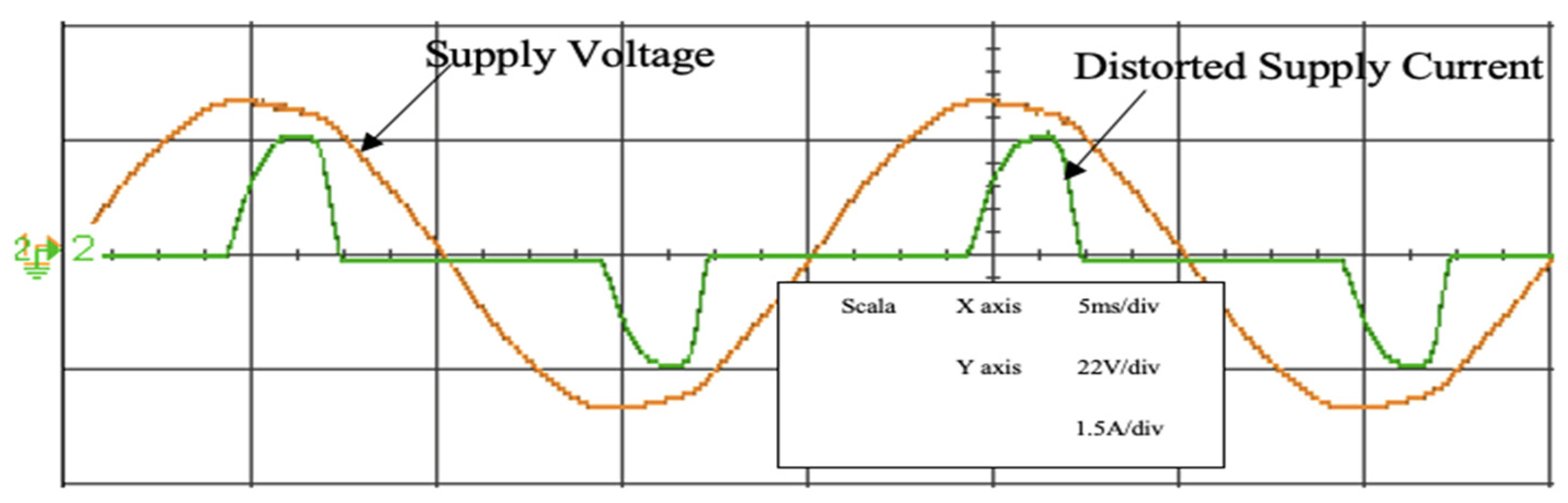
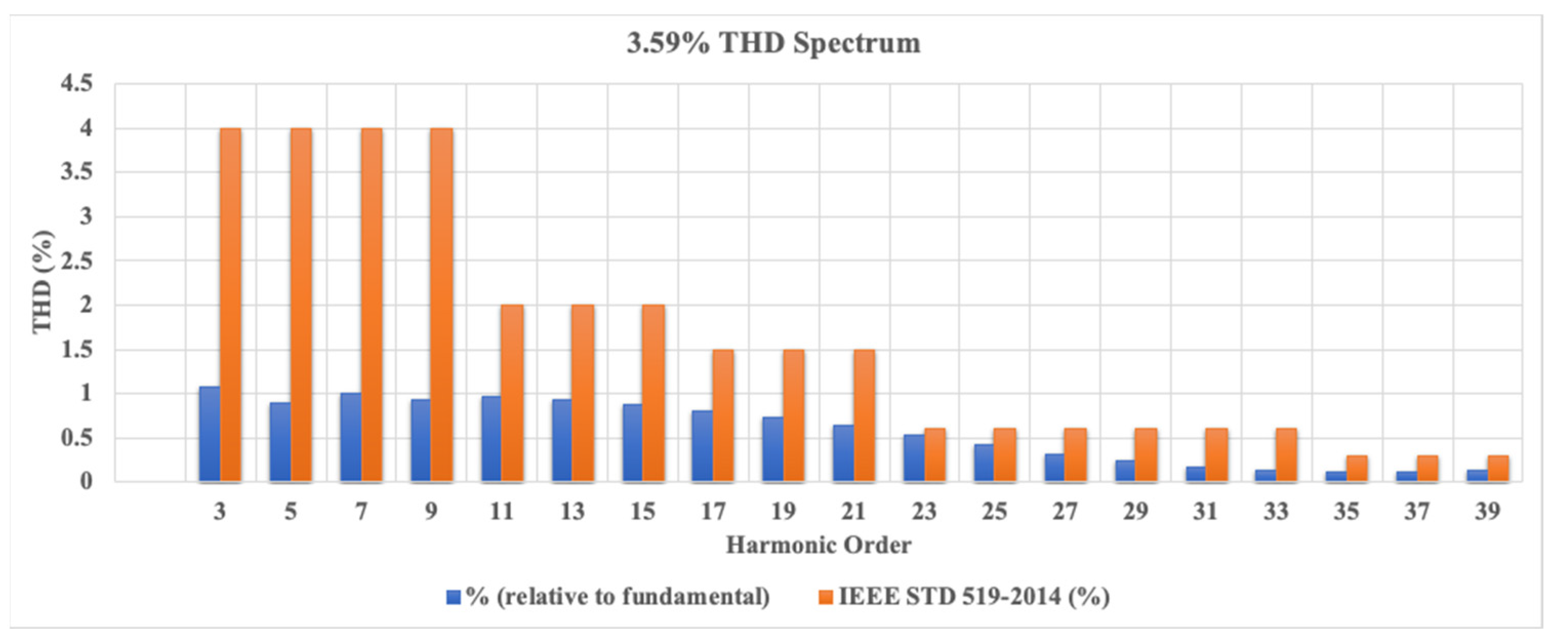
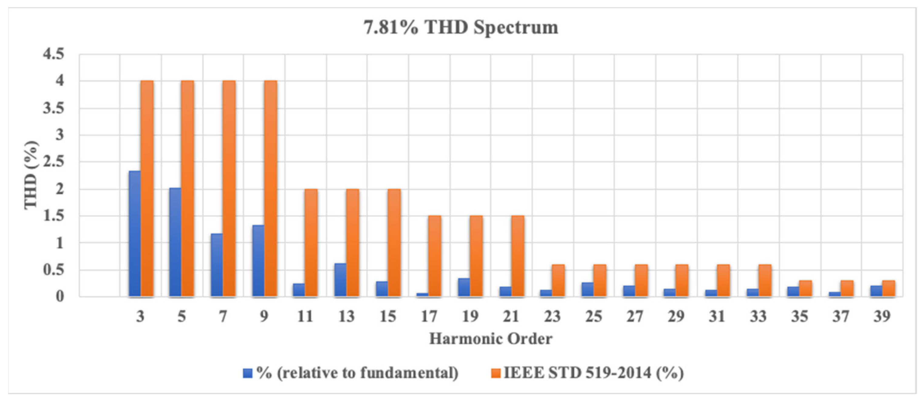
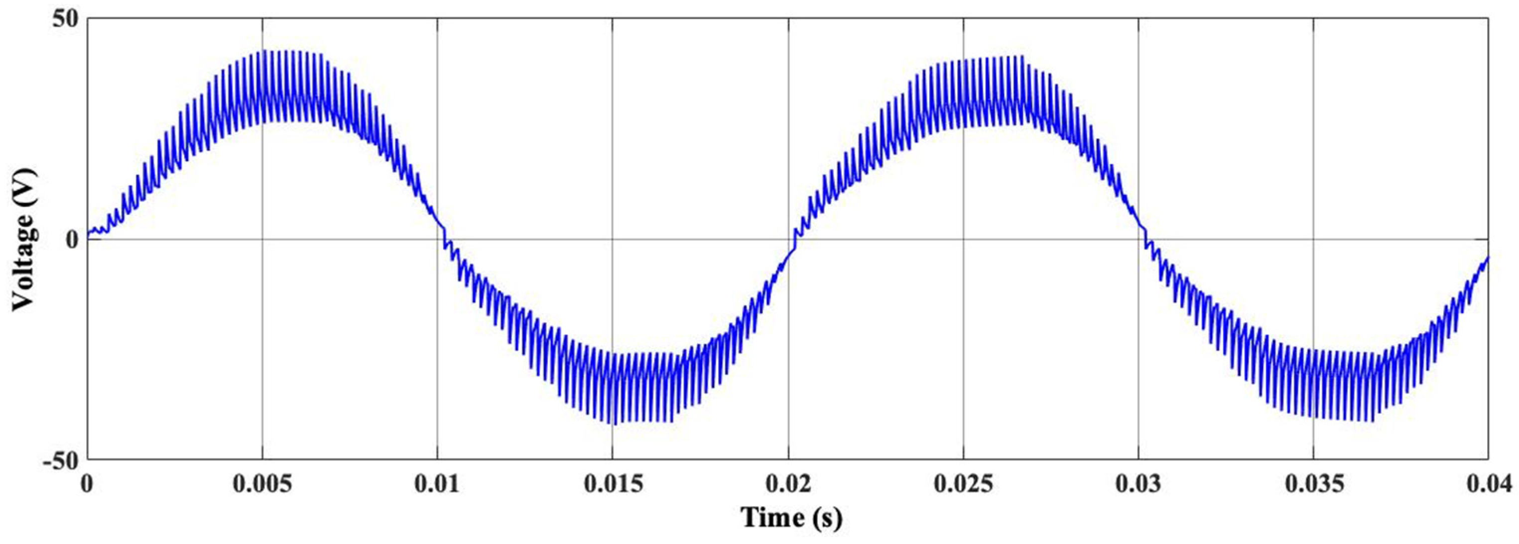
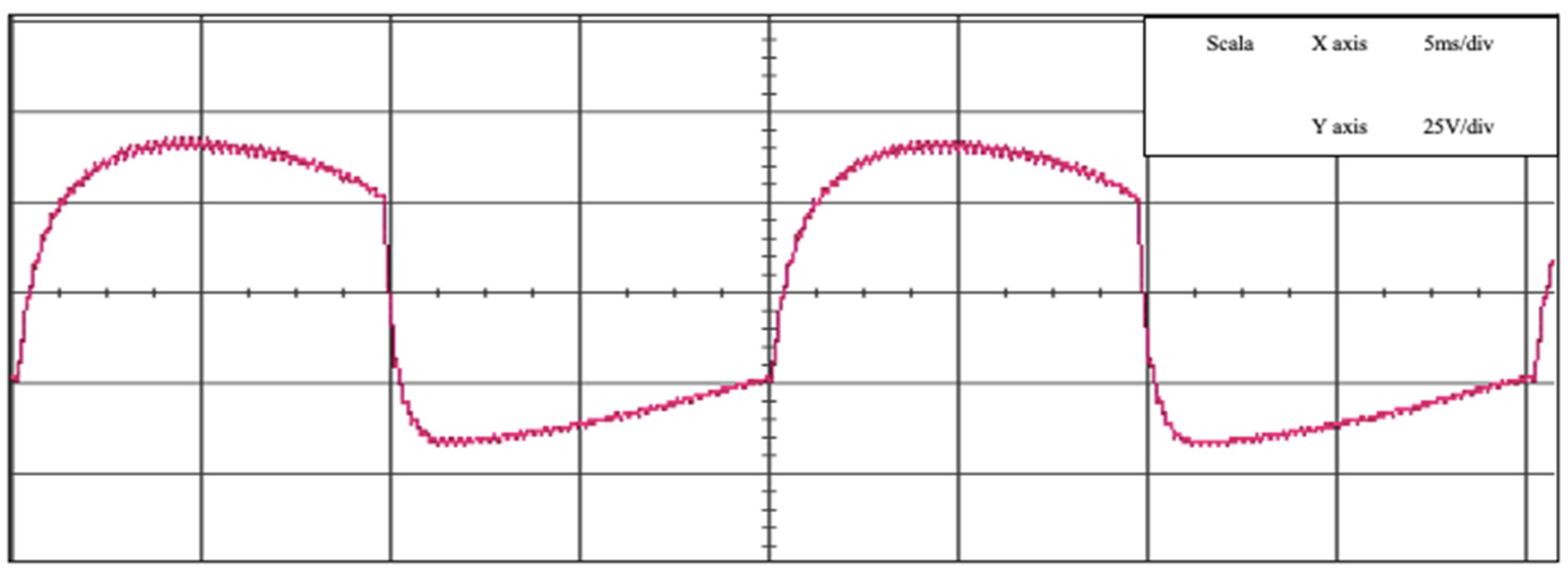
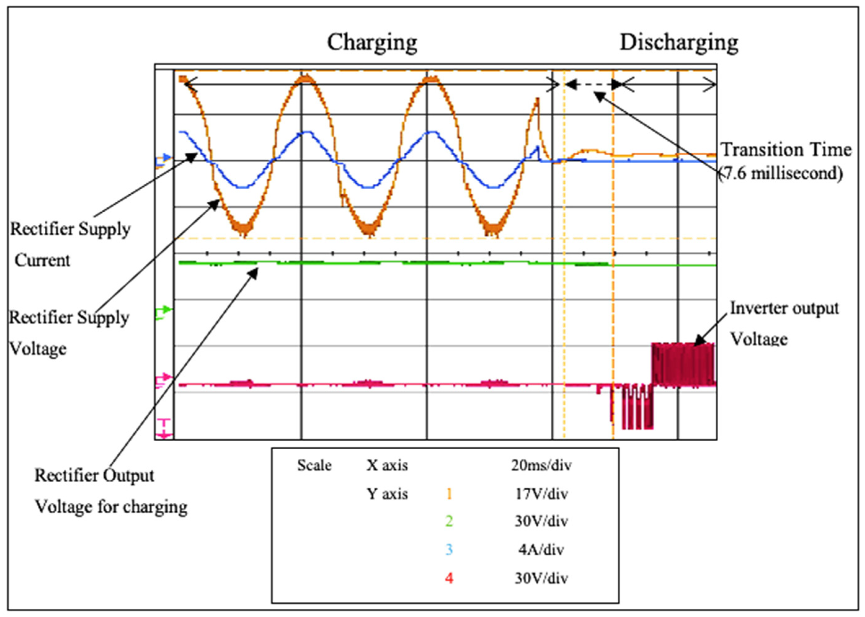
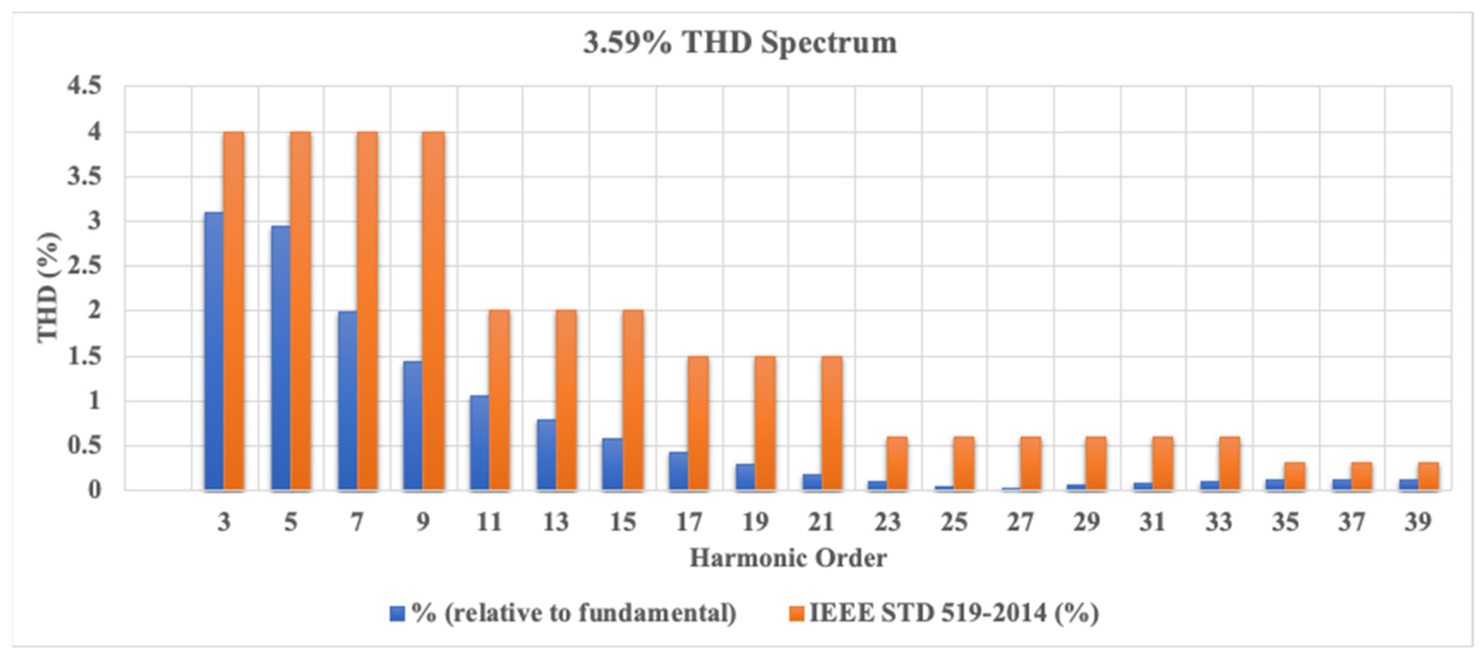
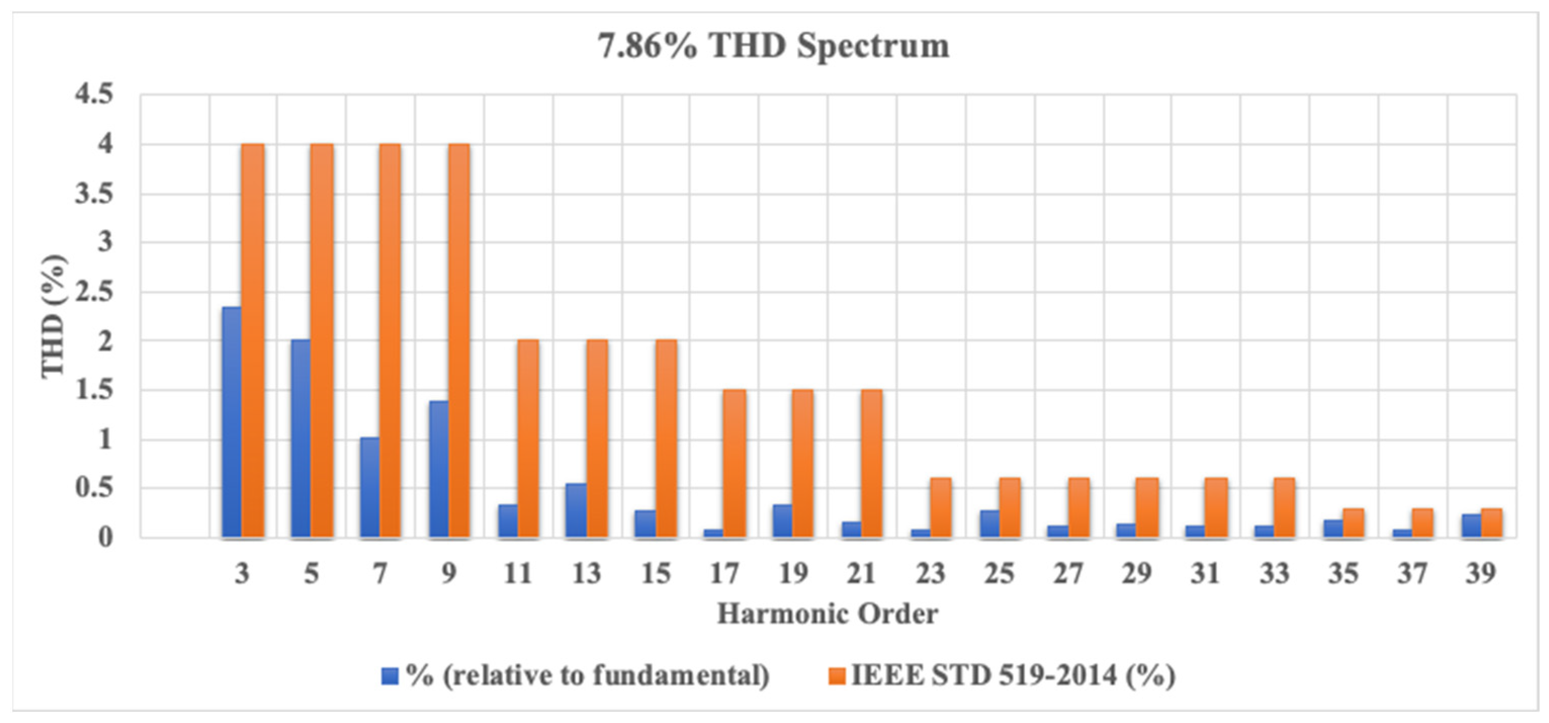
The developed UPS system, based on the SPMC topology, was subjected to simulation within the MATLAB/Simulink environment. As delineated in the preceding discussion, the adoption of a novel switching strategy is pivotal for amalgamating the functionalities of both the rectifier and the inverter, as detailed in Table 3 and Table 4. The specifications for the UPS under consideration are itemized in Table 5, with parameter values aligned with those typically encountered in UPS systems, referencing [24,32,33,34,35].
Figure 24 delineates the circuit’s three primary components of the proposed UPS configuration. In this analysis, a step response methodology is employed to assess the transition duration between the rectifier and inverter phases. Specifically, the rectifier phase is analysed over a sample period from 0 to 0.04 s, while the inverter phase spans from 0.04 to 0.08 s.
To facilitate seamless transitions at t = 0.04 s, a pair of breaker switches are strategically implemented to concurrently manage the supply and load functionalities, as depicted in Figure 24. In the charging phase, from 0 to 0.04 s, the rectifier signal breaker (B) is activated, whereas the inverter signal breaker (A) is deactivated. The shift to inverter operation is initiated at t = 0.04 s, during which B is deactivated, and A is activated, ensuring a smooth transition between operational modes.
In the experimental work, the proposed UPS using SPMC topology was constructed and tested to validate its performance as done in the simulation. In this work, a 24 V AC supply is used to produce at least 15 V output DC voltage to charge a 12 V battery. The 12 V RS 698-8091 Pro Lead-acid batteries are used, which are also well known across several industries and for general purposes. The battery is sealed and ideal for use in UPS and emergency back-up [32].
In the first stage, the Arduino UNO controller is programmed to generate 5-kHz PWM signal to control the SPMC circuit to investigate operation of the controlled rectifier. Further construction has been developed for the controlled rectifier operation using RC load to represent the non-linear load without and with the APF function as shown in Figure 25. This work uses a 10 kHz switching frequency to generate an APWM signal [36].
Next, in the second stage, the construction and implementation of the experimental test rig are continued with the controlled inverter operation as shown in Figure 26. The 12V DC supply from the battery is used in this work, as discussed in the previous subsection. The 5-kHz SPWM signal is used to control the SPMC. The construction and implementation of the controlled inverter are using R and RL loads without and with safe-commutation strategy.
The third stage presents the construction and implementation of the proposed UPS system, as it full schematic diagram is shown in Figure 27. Meanwhile, the experimental test rig is shown in Figure 28.

6. Results

Figure 29 presents the experimental test rig results for the supply current and voltage waveforms using a controlled rectifier with a non-linear load, without the active power filter (APF) function. The results indicate a misalignment and distortion between the supply current and voltage, leading to high total harmonic distortion (THD) levels and reduced efficiency. This distortion adversely affects the supply current waveform, resulting in associated issues such as poor overall power factor, heating effects, device malfunction, and potential damage to other equipment due to nonlinear loads.
The harmonic content of the distorted supply current waveform, as determined through both simulation and experimental means, is showcased in Figure 30 and Figure 31, benchmarked against the IEEE 519-2022 standard [37]. The THD percentages recorded were 189.85% for the simulation and 114.65% for the experimental setup, both exceeding the prescribed standards. These elevated THD levels corroborate prior findings regarding significant harmonic presence, as introduced in Section 1, indicating severe distortion in the supply current that could lead to reduced power factor, overheating, equipment malfunction, and damage.
Comparative analysis of the supply current and voltage for the controlled rectifier equipped with APF functionality is presented in Figure 32 and Figure 33, showing successful harmonic compensation. In the charging mode of operation, the UPS operates with APF function consisting of the absolute circuit for supply distorted current and reference signal, subtractor circuit, PI controller circuit, comparator circuit, and APWM separation circuit to compensate for the distorted supply current waveform to become continuous, sinusoidal and in phase with the supply voltage waveform resulting in high power factor and low THD level.
Further, Figure 34 and Figure 35 display the harmonic spectrum and THD levels for the supply current, adhering to the IEEE 519-2022 Standard, from both simulation and experimental evaluations. THD percentages were found to be significantly lower at 3.59% and 7.81%, respectively, indicating compliance with the standard.
The proposed switching strategy for a controlled boost inverter with a passive filter has demonstrated its efficacy in successfully generating the desired output voltage suitable for grid supply. As evidenced in Figure 36 and Figure 37, the inverter effectively boosts the input voltage of 12 V DC from a battery to generate an output AC voltage of 38 V. This output voltage is sufficient for a transformer to step up the voltage to 415 V AC, which is the required level for grid integration.
Additionally, Figure 38 presents the simulation outcomes for the UPS system’s supply voltage during both charging and discharging phases, utilizing the developed switching algorithm and a step response block to manage transition timing. Operational timings were defined as 0 to 0.04 s for charging and 0.04 to 0.08 s for discharging, aiming to assess the system’s operational fluidity.
Experimental validations are further extended, as shown in Figure 39, which illustrates the supply voltage and current during the UPS system’s charging and discharging modes, demonstrating a harmonious correlation between simulation and experimental data. The transitions between modes were smooth, indicating the controller’s effectiveness in adapting to operational shifts. Notably, the supply current exhibited a sinusoidal form, aligning with the supply voltage, thereby reducing THD levels and enhancing power factor. Simulation results indicated a THD level of 6.59% and a power factor of 0.9996, whereas experimental findings reported a THD of 7.86% and a power factor of 0.9715, as measured by a YOKOGAWA WT333E Digital Power Meter (Yokogawa Test & Measurement Corporation, Tokyo, Japan).
Comparisons of harmonic spectra against the IEEE 519-2022 standard in Figure 40 and Figure 41 confirm that the harmonic levels are within acceptable limits and meet the standard’s requirements. Table 6 consolidates the comparative outcomes for the simulation and experimental setups, both with and without APF functionality, underscoring the APF’s role in diminishing THD levels and improving power factor. The observed discrepancy in THD levels between the simulation and experimental setups can be attributed to the inductive effects of the step-down transformer windings, highlighting the APF function’s critical impact on reducing THD when combined with a suitably designed switching algorithm.

7. Conclusions

This paper elaborates on the effective deployment of a UPS system utilizing SPMC circuit architecture, enhanced with APF capabilities. The designed UPS, an integrated SPMC unit, is adept at fulfilling both rectifying and inverting functions, potentially obviating the need for separate rectifier and inverter circuits found in traditional UPS configurations. The investigation encompassed the UPS’s performance in both charging (rectifier) and discharging (inverter) modes. Furthermore, the incorporation of APF functionality through a boost technique effectively mitigates the fluctuations in the supply current waveform, rendering it continuous, sinusoidal, and synchronized with the supply voltage waveform, thereby elevating the power supply system’s quality. Consequently, the THD of the supply current was significantly diminished to levels below those stipulated by the IEEE519-2022 standard. Moreover, the transition duration between the UPS’s charging and discharging modes aligns with the specifications of the IEC62040-3 standard [38]. This study’s paramount contribution lies in advancing UPS design UPS using SPMC topology, which could be extended for development of various advanced applications such as wireless power charging, fast and high-density micro charging, micro UPS, etc. This is in line with the rapidly evolving global manufacturing landscape that calls for high quality and availability of power supply and can contribute to various applications, from electric vehicles (EVs) to biological implants such as pacemakers in medical technology industries. Future studies could engage in comparative analyses with alternative topologies, assessing higher ratings and efficiency to further endorse the proposed UPS’s potential and applicability.

Author Contributions

Conceptualization, M.S.M.R., R.B. and M.A.M.R.; methodology, M.S.M.R., R.B. and M.A.M.R.; validation, M.S.M.R., R.B. and M.A.M.R.; formal analysis, M.S.M.R., R.B. and M.A.M.R.; investigation, M.S.M.R., R.B. and M.A.M.R.; resources, M.S.M.R., R.B. and M.A.M.R.; writing—original draft preparation, M.S.M.R., R.B. and M.A.M.R.; writing—review and editing, M.S.M.R., R.B. and M.A.M.R.; visualization, M.S.M.R., R.B. and M.A.M.R.; supervision, M.S.M.R., R.B. and M.A.M.R.; project administration, M.S.M.R., R.B. and M.A.M.R.; funding acquisition, M.S.M.R., R.B. and M.A.M.R. All authors have read and agreed to the published version of the manuscript.

Funding

This research was funded by Universiti Teknologi Mara Grant.

Data Availability Statement

Data are contained within the article. To estimate the analyzed results, the authors used raw data from the databases included in Appendix A and Appendix B.

Acknowledgments

Financial support from Faculty of Electrical Engineering Universiti Teknologi MARA (UiTM) is gratefully acknowledged.

Conflicts of Interest

The authors declare no conflicts of interest.

Appendix A

Table A1. Sampling Time for SPWM Generator.
No. of PulsePositive Cycle (μs)No. of PulsePositive Cycle (μs)No. of PulseNegative Cycle (μs)No. of PulseNegative Cycle (μs)
1972614151076132
262754521997773
31882815053278123
4192946541977983
51753015855480112
6313138561958193
71633216557682102
84433315819283104
91503417259108491
105635256018885115
111383617861148679
126837196218487126
131263818463198868
147939146417889138
151154018865259056
169141106617291150
171044219267319244
181024366816593163
19934419569389431
201124547015895175
21834619771469619
221234727215097188
2373481997354986
24132490741419997
25635040075631000

Appendix B

Table A2. Experimental harmonic contents for UPS operation on RC load incorporated with APF function. Total harmonic distortion (THD) = 7.86% and power factor = 0.9715.
Frequency
(Hz)
Harmonic Number% (Relative to Fundamental)Frequency
(Hz)
Harmonic Number% (Relative to Fundamental)
003.401000200.13
501100.001050210.16
10021.031100220.21
15032.341150230.08
20041.861200240.26
25052.011250250.27
30060.891300260.22
35071.021350270.11
40080.591400280.14
45091.391450290.13
500100.521500300.14
550110.341550310.11
600120.311600320.21
650130.541650330.12
700140.571700340.08
750150.281750350.17
800160.181800360.09
850170.071850370.07
900180.201900380.22
950190.341950390.23

Appendix C

Table A3. Simulation result of harmonic contents for UPS Operation on RC load incorporated with APF function using MATLAB/Simulink. Total harmonic distortion (THD) = 3.59% and power factor = 0.9996.
Frequency
(Hz)
Harmonic Number% (Relative to Fundamental)Frequency
(Hz)
Harmonic Number% (Relative to Fundamental)
000.481000200.05
501100.001050210.63
10020.131100220.03
15031.071150230.53
20040.231200240.02
25050.891250250.42
30060.121300260.01
35071.001350270.32
40080.151400280.00
45090.931450290.24
500100.131500300.01
550110.961550310.17
600120.101600320.02
650130.921650330.13
700140.101700340.03
750150.881750350.11
800160.081800360.03
850170.811850370.12
900180.061900380.03
950190.731950390.13

Appendix D

Mathematical modeling of bidirectional switch power losses.
The average power dissipation of a semiconductor device is
P a v g = 1 T 0 T p t d t
where
  • p ( t ) is devices instantaneous dissipated power.
  • T is fundamental output current period.
The power dissipation of a semiconductor device at an arbitrary time instant t is equivalent to the mean conduction and switching losses incurred within the device over the switching period t + T s w subsequent to t [27]. This methodology facilitates the derivation of simplified continuous time power loss expressions by approximating the instantaneous power losses as
P t P c o n d   t + P s w   t = P c o n d   t + P o n   t + P o f f   t
where P c o n d   t and P s w t are the average conduction losses and average switching losses at each switching period, respectively. The switching losses can be classified into two components which are turn-on losses P o n   t and turn-off losses P o f f   t . Turn-on and turn-off losses typically exhibit significant dissipation values in hard-switched commutation topologies, whereas soft-switched commutation results in lower dissipation values. Conversely, clocking losses are generally negligible due to the minimal leakage current of the device in its off-state. Based on the average power losses expression (A1), the total average power can be derived as follows:
P a v g   1 T   0 T P c o n d t d t + 1 T   0 T P o n t d t + 1 T   0 T P o f f t d t
In this research, the UPS circuit schematic using SPMC topology is used. The analyses of power losses for the IGBT and diode are based on one IGBT (for example S1a) and one diode (for example D1b) to calculate SPMC power losses. In the general operation of SPMCs for the positive cycle, the current flows through S1a and D1b and S4a and D4b, and for negative cycle, S2a and D2b and S3a and D3b. The total average power losses of IGBTs (S1a) can be expressed as following:
P S 1 a t P c o n d / S 1 a   t + P s w / S 1 a   t = P c o n d / S 1 a   t + P o n / S 1 a   t + P o f f / S 1 a   t
Meanwhile, the conduction losses of IGBTs (S1a) can be expressed as below:
P c o n d S 1 a t = 1 T s w   t t + T s w V S 1 a t I S 1 a t d t 1 T s w   t t + T c o n d / S 1 a V S 1 a t I S 1 a t d t = V S 1 a t I S 1 a t d t T c o n d / S 1 a T s w = V S 1 a t I S 1 a t D S 1 a ( t ) d t
where V S 1 a   ( t ) is on-state voltage of S1a and I S 1 a   ( t ) can be considered to be equal to the fundamental output current I L   ( t ) during the interval operation of I c o n d / S 1 a   ( t ) if it is assumed that the cycle T s w is infinitely small compared to T. Thus, several equations involved in power losses can be expressed as
I S 1 a   ( t ) I L t = I M   sin ( ω o t )
V S 1 a t = V t / S + a s I S 1 a b S
D S 1 a   t = 1 2 1 + M sin ω o t + φ o
E o n / S 1 a t = h I S 1 a k     ( t )
E o f f / S 1 a t = m I S 1 a n     ( t )
where
  • I M is the output current amplitude.
  • M is the modulation depth index whose value is between 0 to 1.
  • ω 0 is the output frequency pulsation.
Expression (A7) has been described detail in [28]. Thus, the average conduction losses in each switching period, P c o n d / S 1 a   t , can be finally expressed by:
P c o n d / S 1 a   t I M sin ω o t V t / S + a S I S 1 a b s 0.5 1 + Msin ω o t + φ o  
Meanwhile, switching losses of the IGBT (S1a) can also be expressed. The switching power losses are associated to the power dissipated generated during both switching transition on-off and off-on. Thus, the average turn-on losses P o n / S 1 a   t between t and t + T s w , can be calculated as
P o n S 1 a t   1 T s w   t t + t o n V S 1 a t I S 1 a t d t = E o n / S 1 a ( t ) T s w = h I S 1 a k     ( t ) T s w
The average turn-off losses switching period P o f f / S 1 a   t can be expressed as
P o f f S 1 a t   1 T s w   t + t o n + t c o n d / S 1 a t + t o n + t c o n d / S 1 a + t o f f V S 1 a t I S 1 a t d t = E o f f / S 1 a ( t ) T s w = m I S 1 a n     ( t ) T s w
The IGBT average power losses P S 1 a t can be calculated by substituting expression (A6)–(A10):
P S 1 a t = V S 1 a t I S 1 a t D S 1 a t + E o n / S 1 a t T s w + E o f f / S 1 a ( t ) T s w
P S 1 a t = V t S + a S I S 1 a b S I M   sin ω o t 1 2 1 + M sin ω o t + φ o + h I S 1 a k     ( t ) T s w + m I S 1 a n     ( t ) T s w
In analysis of diode circuits, only two primary forms of power loss merit consideration: conduction losses and turn-off losses. The turn-on and blocking losses have been omitted from this analysis due to their negligible contribution to the total power dissipation [28,29]. A detail of the D 1 b schematic instantaneous dissipated power can be appreciated in Figure 5. Thus, P D 1 b t can be described as
P D 1 b t P c o n d / D 1 b   t + P s w / D 1 b   t = P c o n d / D 1 b   t + P o f f / D 1 b   t
P c o n d D 1 b t = 1 T s w   t t + T s w V D 1 b t I D 1 b t d t = 1 T s w   t t + t c o n d / D 1 b + t o f f V D 1 b t I D 1 b t d t = V D 1 b t I D 1 b t D D ( t ) d t
where I D 1 b   t can be considered the fundamental output current and V D 1 b   t is the on-state voltage drop across the diode. Several expressions can be determined as
I D 1 b   ( t ) I L t = I M   sin ( ω o t )
V D 1 b t = V t / D + a D I D 1 b b D
D D   t = 1 2 1 M sin ω o t + φ o
E o f f   / D 1 b t = 0.5 I r r   0.5 V d c t b
The average conduction power losses can be expressed after substituting (A18)–(A20) in (A17) as
P c o n d / D 1 b   t I M sin ω o t V t / D + a D I D 1 b b D 0.5 1 M sin ω o t + φ o  
Meanwhile, switching losses of diode (D1b) can be expressed as below:
P o f f D 1 b t   1 T s w   t + t c o n d / D 1 b t + t c o n d / D 1 b + t o f f V D 1 b t I D 1 b t d t = E o f f / D 1 b ( t ) T s w
Total power losses of diode (D1b) can be expressed as below
P D 1 b t   V D 1 b t I D 1 b t D D t + E o f f / D 1 b ( t ) T s w
Substituting (A18)–(A21) in (A24), then
P D 1 b t = V t / D + a D I D 1 b b D I M   sin ( ω o t ) 1 2 1 M sin ω o t + φ o + 0.5 I r r   0.5 V d c t b T s w

References

  1. Popa, G.N. Electric Power Quality through Analysis and Experiment. Energies 2022, 15, 7947. [Google Scholar] [CrossRef]
  2. Prado, E.O.; Bolsi, P.C.; Sartori, H.C.; Pinheiro, J.R. Comparative Analysis of Modulation Techniques on the Losses and Thermal Limits of Uninterruptible Power Supply Systems. Micromachines 2022, 13, 1708. [Google Scholar] [CrossRef] [PubMed]
  3. Godoy, M.P.; Uberti, V.A.; da Rosa Abaide, A.; Guidali, G.D.; Prade, L.R.; Keller, A.L. Identifying and reducing harmonic distortion in an industrial uninterruptible power supply system. In Proceedings of the 2020 6th International Conference on Electric Power and Energy Conversion Systems (EPECS), Istanbul, Turkey, 5–7 October 2020; pp. 34–39. [Google Scholar]
  4. Abaray, S.; Beaver, S.; Nguyen, C. How reliable is your ups? Eliminating single points of failure. In Proceedings of the 2017 Petroleum and Chemical Industry Technical Conference (PCIC), Calgary, AB, Canada, 18–20 September 2017; pp. 311–316. [Google Scholar]
  5. Srivastava, M.; Goyal, S.K.; Saraswat, A.; Shekhawat, R.S.; Gangil, G. A Review on Power Quality Problems, Causes and Mitigation Techniques. In Proceedings of the 2022 1st International Conference on Sustainable Technology for Power and Energy Systems (STPES), SRINAGAR, India, 4–6 July 2022; pp. 1–6. [Google Scholar]
  6. Gerber, D.L.; Ghatpande, O.A.; Nazir, M.; Heredia, W.G.B.; Feng, W.; Brown, R.E. Energy and power quality measurement for electrical distribution in AC and DC microgrid buildings. Appl. Energy 2022, 308, 118308. [Google Scholar] [CrossRef]
  7. Gong, S.; Huang, J.; He, G. Research on ADRC controller design for three-phase UPS with multi-disturbances. J. Eng. 2019, 2019, 8409–8413. [Google Scholar] [CrossRef]
  8. Kim, J.; Choi, H.H.; Jung, J.W. MRAC-Based voltage controller for three-phase CVCF inverters to attenuate parameter uncertainties under critical load conditions. IEEE Trans. Power Electron. 2020, 35, 1002–1013. [Google Scholar] [CrossRef]
  9. Kumar, M.; Uqaili, M.A.; Memon, Z.A.; Das, B. Experimental Harmonics Analysis of UPS (Uninterrupted Power Supply) System and Mitigation Using Single-Phase Half-Bridge HAPF (Hybrid Active Power Filter) Based on Novel Fuzzy Logic Current Controller (FLCC) for Reference Current Extraction (RCE). Adv. Fuzzy Syst. 2022, 2022, 5466268. [Google Scholar] [CrossRef]
  10. Vyas, M.; Vyas, S. Matrix Converter: A Solution for Electric Drives and Control Applications. In Optimal Planning of Smart Grid With Renewable Energy Resources; IGI Global: Hershey, PA, USA, 2022; pp. 219–244. [Google Scholar]
  11. Burhanudin, J.; Hasim, A.S.A.; Ishak, A.M.; Fairuz, S.M.; Dardin, S.M.; Azid, A.A.; Burhanudin, J. Simulation of AC/ AC Converter using Single Phase Matrix Converter for Wave Energy Converter. In Proceedings of the 2022 IEEE International Conference in Power Engineering Application (ICPEA), Shah Alam, Malaysia, 7–8 March 2022; pp. 1–6. [Google Scholar]
  12. Osheba, M.S.; Lashine, A.E.; Mansour, A.S. Design, implementation and performance evaluation of multi-function boost converter. Sci. Rep. 2023, 13, 4276. [Google Scholar] [CrossRef] [PubMed]
  13. Gyugyi, B.; Pelly, L. Static Power Chargers, Theory, Performance and Application; John Wiley & Son Inc.: Hoboken, NJ, USA, 1976; Volume 1. [Google Scholar]
  14. Narwal, R.; Rawat, S.; Kanale, A.; Cheng, T.H.; Agarwal, A.; Bhattacharya, S.; Baliga, B.J.; Hopkins, D.C. Analysis and Characterization of Four-quadrant Switches based Commutation Cell. In Proceedings of the 2023 IEEE Applied Power Electronics Conference and Exposition (APEC), Orlando, FL, USA, 19–23 March 2023; pp. 209–216. [Google Scholar]
  15. Rahman, K. Matrix converter and its probable applications. In DC Microgrids: Advances, Challenges, and Applications; Wiley: Hoboken, NJ, USA, 2021; pp. 273–298. [Google Scholar]
  16. Zuckerberger, A.; Weinstock, D.; Aiexandrovitz, A. Single-phase matrix converter. IEE Proceeding Electr. Power Appl. 1997, 144, 235–240. [Google Scholar] [CrossRef]
  17. Burany, N. Safe control of four-quadrant switches. In Proceedings of the Conference Record of the IEEE Industry Applications Society Annual Meeting, San Diego, CA, USA, 1–5 October 1989; Volume 1, pp. 1190–1194. [Google Scholar]
  18. Baharom, R.; Hamzah, M.K. A New Single-Phase Controlled Rectifier Using Single-Phase Matrix Converter Topology Incorporating Active Power Filter. In Proceedings of the 2007 IEEE International Electric Machines & Drives Conference, Antalya, Turkey, 3–5 May 2007; pp. 874–879. [Google Scholar]
  19. Osman, D.A.A.; Baharom, R.; Johari, D.; Hidayat, M.N.; Muhammad, K.S. Development of active power filter using rectifier boost technique. Int. J. Power Electron. Drive Syst. 2019, 10, 1446–1453. [Google Scholar] [CrossRef]
  20. Vázquez, N.; Aguilar, C.; Arau, J.; Cáceres, R.O.; Barbi, I.; Gallegos, J.A. A novel uninterruptible power supply system with active power factor correction. IEEE Trans. Power Electron. 2002, 17, 405–412. [Google Scholar] [CrossRef]
  21. Hamzah, M.K.; Saidon, M.F.; Noor, S.Z.M. Application of Single-Phase Matrix Converter Topology in Uninterruptible Power Supply Circuit incorporating Unity Power Factor Control. In Proceedings of the 2006 1ST IEEE Conference on Industrial Electronics and Applications, Singapore, 24–26 May 2006; pp. 1–6. [Google Scholar]
  22. Baharom, R.; Rawi, M.S.M.; Rahman, N.F.A. Uninterruptible Power Supply Employing Single-Phase Matrix Converter Topology. In Proceedings of the 2020 IEEE International Conference on Power and Energy (PECon), Penang, Malaysia, 7–8 December 2020; pp. 19–23. [Google Scholar]
  23. Rawi, M.M.S.; Baharom, R.; Radzi, M.A.M. Simulation Model of Uninterruptible Wireless Power Supply Based on Single-Phase Matrix Converter with Active Power Filter Functionality. In Proceedings of the 2023 IEEE Industrial Electronics and Applications Conference (IEACon), Penang, Malaysia, 6–7 November 2023; pp. 157–162. [Google Scholar]
  24. Rawi, M.S.M.; Baharom, R.; Rahman, N.F.A. Computer Simulation Model of Unity Power Factor Uninterruptible Power Supply Topology using Single Phase Matrix Converter; International Journal of Power Electronics and Drive Systems (IJPEDS): Yogyakarta, Indonesia, 2022; Volume 12, pp. 969–979. [Google Scholar]
  25. Wang, B.; Venkataramanan, G. Analytical modeling of semiconductor losses in matrix converters. In Proceedings of the Conference Proceedings—IPEMC 2006: CES/IEEE 5th International Power Electronics and Motion Control Conference, Shanghai, China, 14–16 August 2006; Volume 1, pp. 1–8. [Google Scholar]
  26. Robinson, F.V.P. Power electronics converters, applications and design. Microelectronics J. 1997, 28, 105–106. [Google Scholar] [CrossRef]
  27. Clemente, S. Application characterization of IGBTs. In Application Note AN-990, IGBT Design Manual; International Rectifier: El Segundo, CA, USA, 1994. [Google Scholar]
  28. PEM, “Power Electronic Measurement. Available online: Https://www.pemuk.com (accessed on 18 June 2024).
  29. Casanellas, F. Losses in PWM inverters using IGBTs. IEE Proc. Electr. Power Appl. 1994, 141, 235–239. [Google Scholar] [CrossRef]
  30. Dalai, S.K.; Dash, D.K. Analysis of single-phase matrix converter with regenerative capabilities of Single phase induction motor. In Proceedings of the 2017 International Conference on Smart Technologies for Smart Nation (SmartTechCon), Bengaluru, India, 17–19 August 2017; pp. 465–469. [Google Scholar]
  31. Baharom, R.; Hashim, N.; Hamzah, M.K. Implementation of controlled rectifier with power factor correction using single-phase matrix converter. In Proceedings of the 2009 International Conference on Power Electronics and Drive Systems (PEDS), Taipei, Taiwan, 2–5 November 2009; pp. 1020–1025. [Google Scholar]
  32. Ramesh, R.D.K.K.S. An Investigation on Performance Characteristics of Sealed Lead Acid Battery. In Proceedings of the 2022 4th International Conference on Smart Systems and Inventive Technology (ICSSIT), Penang, Malaysia, 6–7 November 2023; pp. 563–568. [Google Scholar]
  33. Bradley, A. DC-UPS with Integrated Battery-24V, 10A; Rockwell Automation Publication: Milwaukee, WI, USA, 2019; 1606-RM003A-EN-P; Available online: https://literature.rockwellautomation.com/idc/groups/literature/documents/rm/1606-rm003_-en-p.pdf (accessed on 18 June 2024).
  34. Youssef, M. Simulation and Design of A Single Phase Inverter with Digital PWM Issued by An Arduino Board. Int. J. Eng. Res. Technol. 2020, 9, 560–566. [Google Scholar]
  35. Li, J. Measuring and Understanding the Output Voltage Ripple of A Boost Converter; Texas Instruments Inc.: Dallas, TX, USA, 2021. [Google Scholar]
  36. Zin, M.F.M.; Baharom, R.; Yassin, I.M. Development of boost inverter using single phase matrix converter topology. Int. J. Eng. Technol. 2018, 7, 241–245. [Google Scholar]
  37. IEEE Std 519™-2022; IEEE Standard for Harmonic Control in Electric Power Systems. The Institute of Electrical and Electronics Engineers Inc.: New York, NY, USA, 2022.
  38. IEC62040-3 Standard; Uninterruptible Power Systems (UPS)-Part 3: Method of Specifying the Performance and Test Requirements. International Electrotechnical Commission: Geneva, Switzerland, 2021.
Figure 1. Typical UPS system.
Energies 17 03441 g001
Figure 2. SPMC topology and its bidirectional switch.
Energies 17 03441 g002
Figure 3. Schematic instantaneous IGBT power losses in a T s w interval.
Energies 17 03441 g003
Figure 4. SPMC topology circuit bidirectional switch (IGBTs and diodes).
Energies 17 03441 g004
Figure 5. Schematic instantaneous of diode power losses in T s w interval.
Energies 17 03441 g005
Figure 6. The proposed UPS system.
Energies 17 03441 g006
Figure 7. The proposed UPS circuit without filter.
Energies 17 03441 g007
Figure 8. Comparison waveforms of rectifier connected to RC load (a) without APF and (b) with APF.
Energies 17 03441 g008
Figure 9. Rectifier with CCL.
Energies 17 03441 g009
Figure 10. Boost inductor with SPMC circuit.
Energies 17 03441 g010
Figure 11. Waveforms for mathematical treatment of boost inductor.
Energies 17 03441 g011
Figure 12. Circuit for mathematical treatment of boost inductor.
Energies 17 03441 g012
Figure 13. Peak-to-peak ripple current.
Energies 17 03441 g013
Figure 14. Circuit of APF configuration by (a) charging inductor and (b) discharging inductor.
Energies 17 03441 g014
Figure 15. Stage configuration of CCL.
Energies 17 03441 g015
Figure 16. Absolute circuit of CCL.
Energies 17 03441 g016
Figure 17. Schematic diagram of subtractor circuit.
Energies 17 03441 g017
Figure 18. PI controller circuit.
Energies 17 03441 g018
Figure 19. Schematic diagram of controlled rectifier mode in UPS: (a) positive and (b) negative cycles.
Energies 17 03441 g019
Figure 20. Schematic diagram of controlled inverter mode in UPS: (a) positive and (b) negative cycles.
Energies 17 03441 g020
Figure 21. Generation of SPWM signal for half-, positive, and negative cycles by using Arduino Uno Controller.
Energies 17 03441 g021
Figure 22. Waveform pattern of switching pulse for the controlled inverter with boost operation.
Energies 17 03441 g022
Figure 23. The waveforms of charging (rectifier operation) and discharging (inverter operation) modes.
Energies 17 03441 g023
Figure 24. Three main blocks of the proposed UPS.
Energies 17 03441 g024
Figure 25. Schematic diagram of controlled rectifier incorporated with APF function.
Energies 17 03441 g025
Figure 26. Schematic diagram of controlled inverter operation.
Energies 17 03441 g026
Figure 27. Full schematic diagram of UPS system.
Energies 17 03441 g027
Figure 28. Experimental test rig for the proposed UPS system.
Energies 17 03441 g028
Figure 29. Experimental findings for supply current and voltage utilizing the controlled rectifier devoid of APF.
Energies 17 03441 g029
Figure 30. Harmonic distribution of the distorted supply current derived from simulation data of the controlled rectifier lacking APF.
Energies 17 03441 g030
Figure 31. Harmonic profile of the distorted supply current from experimental observations of the controlled rectifier without APF.
Energies 17 03441 g031
Figure 32. Simulation findings for supply current and voltage using the controlled rectifier equipped with APF.
Energies 17 03441 g032
Figure 33. Experimental outcomes for supply current and voltage from the controlled rectifier integrated with APF.
Energies 17 03441 g033
Figure 34. Harmonic analysis of the supply current from simulation data of the controlled rectifier incorporating APF.
Energies 17 03441 g034
Figure 35. Harmonic profile of the supply current derived from experimental findings of the controlled rectifier with APF.
Energies 17 03441 g035
Figure 36. Simulation outcomes for the output voltage of the controlled boost inverter equipped with a passive filter.
Energies 17 03441 g036
Figure 37. Experimental findings for the output voltage from the controlled boost inverter using a passive filter.
Energies 17 03441 g037
Figure 38. Simulation outcomes depicting the supply voltage waveform in charging mode and the output voltage waveform in discharging mode.
Energies 17 03441 g038
Figure 39. Experimental findings illustrating the waveform of supply voltage during charging mode and the waveform of output voltage during discharging mode.
Energies 17 03441 g039
Figure 40. Harmonic analysis of the supply current derived from simulation data for the controlled inverter integrated with APF.
Energies 17 03441 g040
Figure 41. Harmonic distribution of the supply current from experimental outcomes for the controlled inverter equipped with APF.
Energies 17 03441 g041
Table 1. Parameter for IGBT and diode power losses.
StateIGBT ParametersDiode Parameter
On-state V t / S = 0.875 ,   a S = 0.028 ,   b s = 0.745 V t / D = 0.8 ,   a D = 0.005 ,   b D = 1
Turn-on h = 1.21 × 10 3   m J , k = 1.65 , -
Turn-off m = 0.027 × 10 3   m J , n = 1.183 p e a k   I r r = 25, t b = 0.030   µ s
Applied voltage V d c = 12   V
Fundamental frequency f o u t = 50   H z
Switching frequency f s w = 5   K H z
Modulation M = 0.75
Peak current I M = 1   A
Power factor φ = 0.74 r a d
Table 2. Number of switches used in UPS.
DeviceTotal Losses/DeviceProposed UPSTypical UPS
Number of Devices (Losses)Number of Devices (Losses)
IGBT41.45 W8 (331.6 W)4 (165.8 W)
DIODE15.50 W8 (124 W)8 (124 W)
Total Losses56.95 W455.6 W289.8 W
Table 3. Switching strategy for rectifier operation.
SwitchRectifier Mode
Positive CycleNegative Cycle
S1aONOff
S1bOffAPWM
S2aOffOff
S2bOffON
S3aAPWMOff
S3bOffON
S4aONOff
S4bOffOff
Table 4. Switching algorithm of inverter operation mode for UPS system.
Inverter OperationPositive CycleNegative Cycle
Switching Starting PulseSwitchingStarting Pulse
S1aOffOffOffOff
S1bONHighOffOff
S2aOffOffONHigh
S2bOffOffOffOff
S3aSPWMLowSPWMHigh
S3bOffOffOffOff
S4aOffOffOffOff
S4bSPWMLowSPWMHigh
Table 5. Parameters for experimental test rig.
ParameterValue
AC supply voltage, Vac24 V
DC supply voltage, Vdc12 V
Boost inductor, Ls2 mH
Inductor load, LL5 mH
Capacitor load, CL1000 μF
Resistive load, RL300 Ω
Switching frequency for rectifier, fs10 kHz
Switching frequency for inverter, fs5 kHz
Proportional gain, Kp8
Integral gain, Ki27
Table 6. Performance Comparison of Simulation and Experimental Test rig.
StrategiesTHD (%)Power Factor (pf)
Rectifier without APF Simulation189.850.6248
Experimental test rig114.650.6391
Rectifier with APFSimulation3.590.9996
Experimental test rig7.810.9725
UPS with APFSimulation3.590.9996
Experimental test rig7.860.9715
Disclaimer/Publisher’s Note: The statements, opinions and data contained in all publications are solely those of the individual author(s) and contributor(s) and not of MDPI and/or the editor(s). MDPI and/or the editor(s) disclaim responsibility for any injury to people or property resulting from any ideas, methods, instructions or products referred to in the content.

