Article

A Reconfigurable Phase-Shifted Full-Bridge DC–DC Converter with Wide Range Output Voltage

by
Jhon Brajhan Benites Quispe
1,
Marcello Mezaroba
2,
Alessandro Luiz Batschauer
2 and
Jean Marcos de Souza Ribeiro
1,*
1
Department of Electrical Engineering, São Paulo State University, Ilha Solteira 15385-000, Brazil
2
Department of Electrical Engineering, Santa Catarina State University, Joinville 89219-710, Brazil
*
Author to whom correspondence should be addressed.
Energies 2024, 17(14), 3483; https://doi.org/10.3390/en17143483
Submission received: 31 May 2024 / Revised: 29 June 2024 / Accepted: 9 July 2024 / Published: 15 July 2024

Abstract

:
This paper analyzes, designs and implements a reconfigurable phase-shifted full-bridge (PSFB) converter. It adopts the topology of the traditional PSFB converter and incorporates clamping circuits to solve some fundamental problems of conventional topology. In addition, auxiliary switches are employed for output reconfiguration, which allows expanding the output voltage range without compromising the system efficiency. Single pole double throw (SPDT) mechanical switches are used to realize series and parallel connections. In this paper, the characterization of the PSFB converter with clamping circuit and its design considerations are discussed. A 10 kW prototype with a power density of 0.485 W/cm3, 900 V input voltage and 400/800 V nominal output voltage was manufactured. The experimental results validated the analysis and confirmed the high conversion efficiency for a wide load range; an efficiency of 96.69% was obtained for the full load condition.

1. Introduction

The phase-shifted full-bridge (PSFB) converter is very attractive for medium- and high-power applications due to its high efficiency and power density [1,2]. It is widely used in many modern industrial fields, such as renewable energy conversion [3,4] and electric vehicle (EV) charging [5]. The phase-shift pulse-width modulation technique provides zero voltage switching (ZVS) in the primary-side switches by introducing a phase-shift angle between the half-bridge legs [6,7]. The traditional PSFB converter features simple structure, natural soft-swiching, isolation capability and simple control. However, it has some well-known drawbacks that need to be resolved, such as narrow ZVS range, circulating current, duty-cycle loss, secondary parasitic oscillation and large output filter [8].
Several modified PSFB converters have been proposed to overcome the aforementioned problems [9,10,11,12,13,14,15,16,17,18,19,20,21,22,23,24]. In [9,10], the range of ZVS operation is extended by utilizing the stored energy in passive auxiliary circuits. However, these increase conduction loss and the circulating current cannot be eliminated. In [11,12], passive auxiliary circuits with adaptive ZVS energy reduce conduction loss, but the circulating current still exists. In [13,14], active auxiliary circuits with zero-voltage zero-current switching (ZVZCS) operation are adopted to eliminate the circulating current. In [15,16], the active switches are employed in secondary side and the circulating current is suppressed by adjusting the phase-shifted angle between primary and secondary switches. However, these active auxiliary circuits increase the complexity of the converter due to additional driver circuits. The hybrid-type converters proposed in [17,18] are another solution to remove the circulating current and expand the ZVS range. But many auxiliary components are required, and the improvements of cost and power density are limited. In order to mitigate the voltage oscillation across the rectifier diodes, a resistor–capacitor–diode (RCD) clamp circuit is generally used [19]. However, it causes considerable losses and reduces the efficiency of the converter. In [20], two clamping diodes on the primary side are employed to clamp the voltage across the secondary side rectifier diodes. But the added diodes cannot eliminate the circulating current. In [21], a capacitor–diode–diode (CDD) clamp circuit is used on the secondary side to reduce the voltage stress on these rectifier diodes. However, a large output capacitor is necessary to cover the large ripple current, which consequently reduces power density. In [22,23], a CDD clamp circuit with center tap of the transformer on the secondary side is employed. This simple clamp mechanism, which is detailed in [24], can solve several drawbacks of the traditional PSFB converter. However, simplified mathematical analysis and conservative design constraints are some shortcomings to be resolved.
PSFB converters are widely used in EV charging applications. Currently, most manufacturers adopt the 400 V battery voltage architecture, but new EV models with 800 V battery voltage architecture are being introduced into the market. Therefore, power electronic converters that operate with extremely wide battery voltage ranges are necessary. In [25,26], the idea of reconfigurable PSFB converters is proposed, where a wide range input and output voltage is realized by controlling several auxiliary switches to enable the series and parallel reconfigurations on the primary and secondary side. In [27], a reconfigurable PSFB converter prototype with RCD snubbers is developed, in which three mechanical switches are employed to realize the series or parallel connection on the secondary side of the converter. Therefore, this paper designs and implements a reconfigurable PSFB converter with CDD clamp circuits, where series and parallel reconfigurations on the secondary side are enabled by two single pole double throw (SPDT) mechanical switches. Furthermore, an extended analysis of the CDD clamp mechanism is elaborated on.
The proposed reconfigurable PSFB converter has reduced complexity compared to state-of-the-art solutions and is primarily designed to provide a wide range output voltage. The paper is organized as follows: Section 2 presents a comprehensive description of the proposed reconfigurable PSFB converter system. Section 3 describes the prototype and discusses the experimental results. Finally, Section 4 presents the study conclusions.

2. Materials and Methods

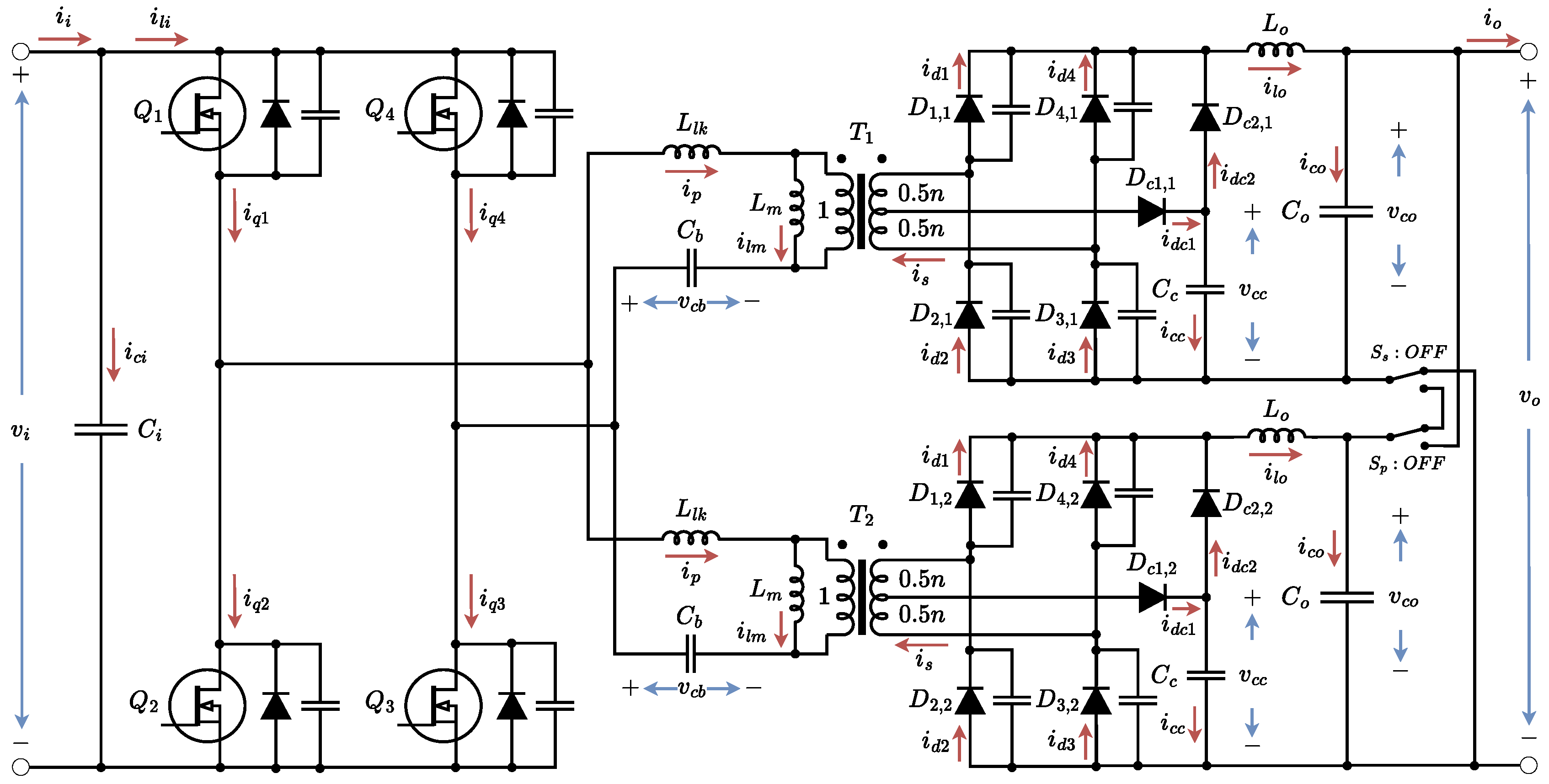
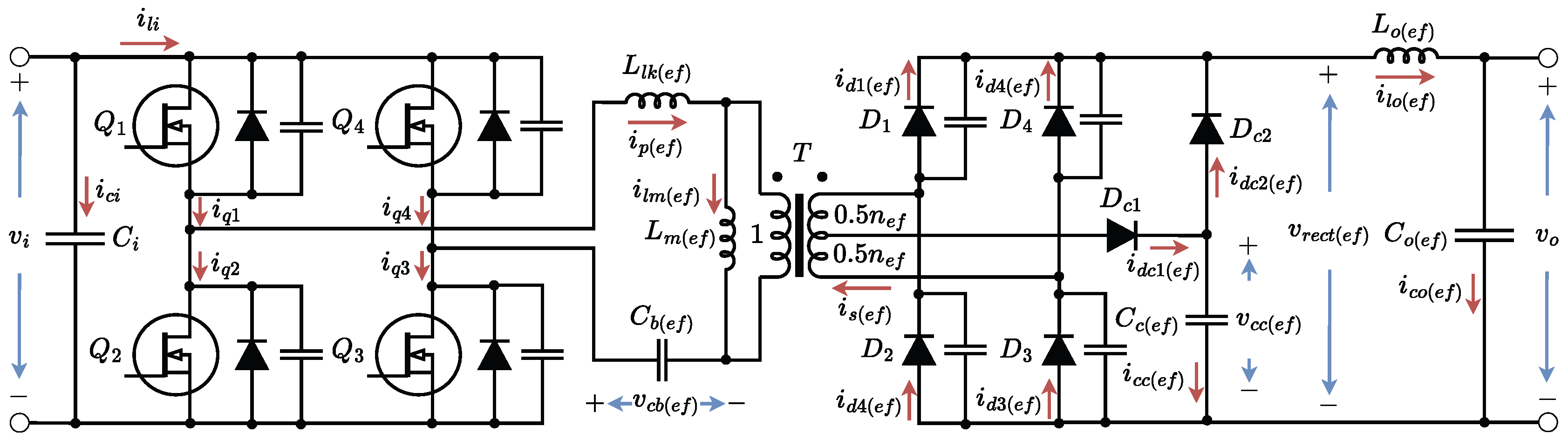
2.1. Circuit Description

The circuit diagram of the proposed reconfigurable PSFB converter is shown in Figure 1. Two transformers are used, which have a primary winding and a secondary winding with a center tap connected to a CDD clamp circuit. An equivalent series inductance L l k that represents an external series inductance added to the leakage inductance of the transformer is present in the primary sides. In addition, a blocking capacitor C b is added in the primary sides to eliminate DC current in transformers. The primary sides are connected in parallel and fed by an FB inverter. Each of the secondary sides is connected to an FB rectifier, a CDD clamp circuit and an LC output filter. Two auxiliary switches, S s and S p , connect the two secondary sides and enable series and parallel reconfigurations according to their switching states. When S s is kept ON and S p is maintained at OFF, the two secondary sides are connected in series. Conversely, when S p is kept ON and S s is maintained at OFF, the two secondary sides are connected in parallel.

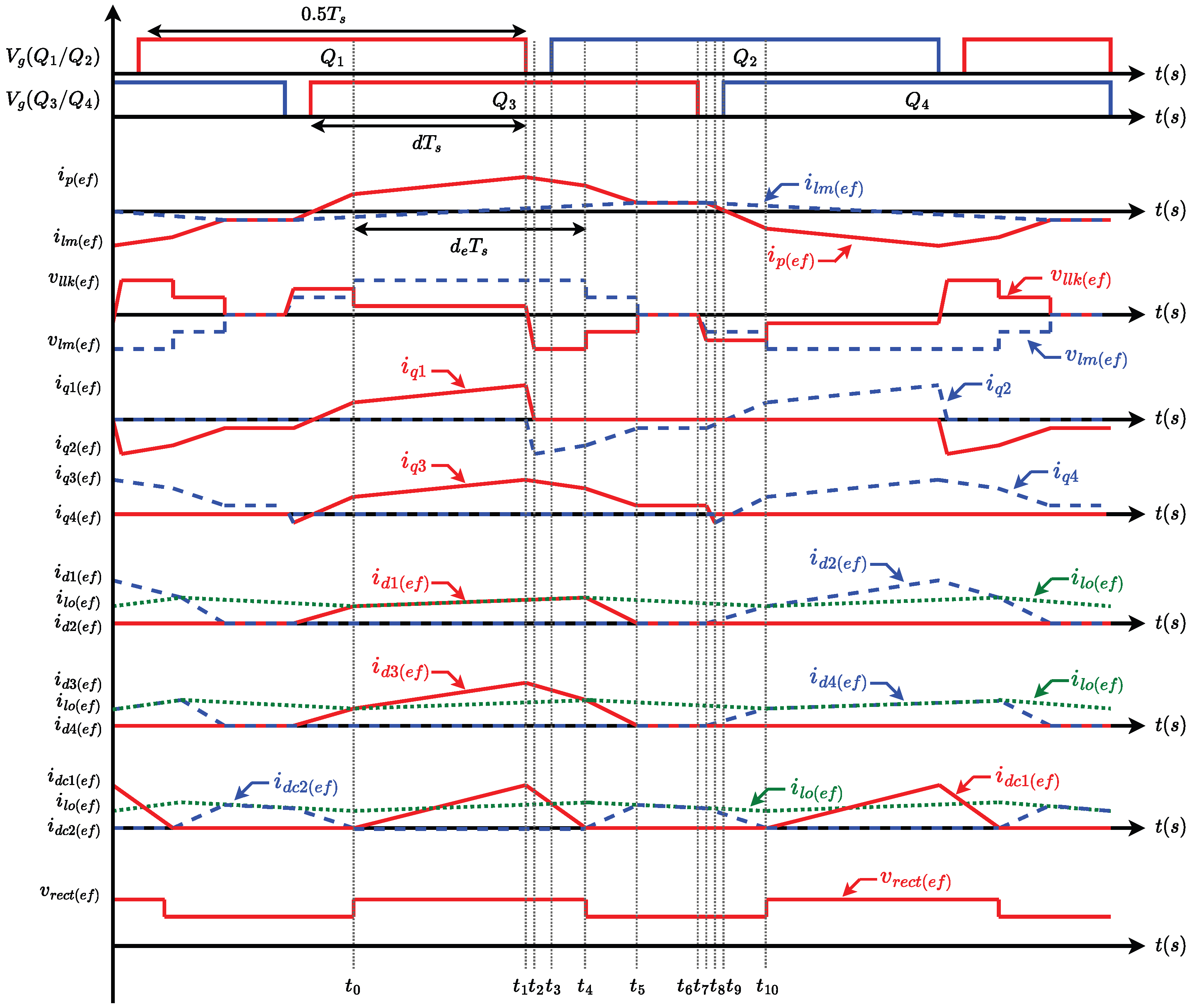
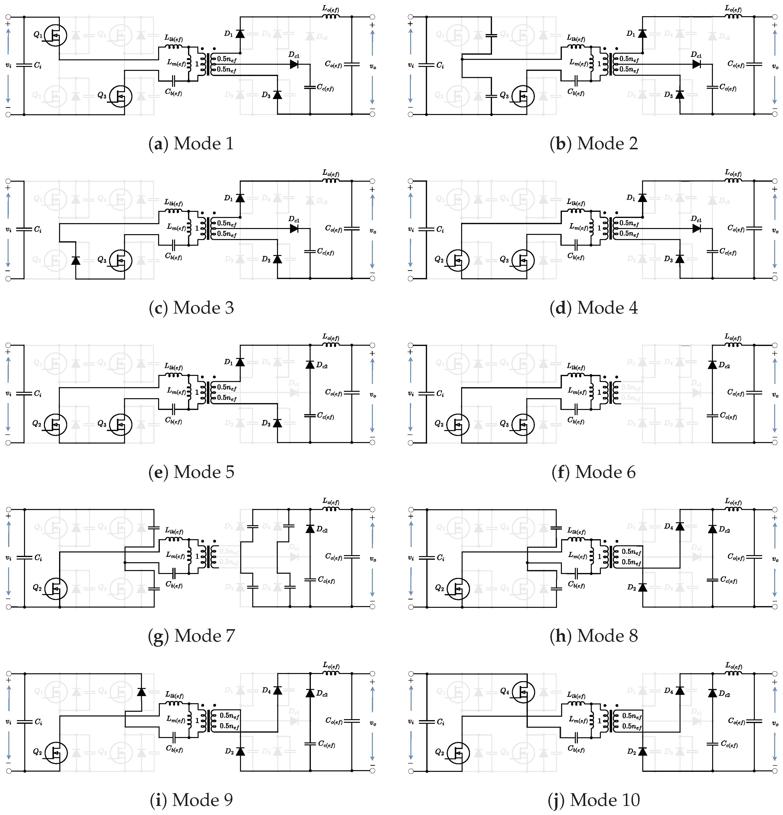
2.2. Operation Analysis

The proposed reconfigurable PSFB converter can be seen as equivalent to a traditional PSFB converter with a CDD clamp circuit, being either the series or parallel connection configuration. The equivalent circuit of the proposed reconfigurable PSFB converter is shown in Figure 2. Table 1 lists the equivalent circuit parameters.
The control method is pulse-width modulation with phase-shift. Figure 3 shows the key waveforms of the equivalent circuit in Figure 2. Each switching period T s is divided into two half-cycles, where each half-cycle is subdivided into ten operation modes. Since the operation modes are symmetrical, only one half-cycle is analyzed. The equivalent operation circuits are shown in Figure 4. In order to analyze the operation modes, the following assumptions are made to simplify analysis: (1) The clamping capacitance C c ( e f ) is sufficiently large to be treated as a constant voltage source. (2) The output filter inductance L o ( e f ) is sufficiently large to be treated as a constant current source. (3) The blocking capacitance C b ( e f ) is sufficiently large to be treated as a negligible constant voltage source. (4) The transformer is ideal, except for its leakage inductance L l k ( e f ) and magnetizing inductance L m ( e f ) . (5) MOSFETs Q 1 Q 4 are identical and ideal, except for their output parasitic capacitances C o s s and body diodes. (6) The rectifier diodes D 1 D 4 are identical and ideal, except for their junction capacitances. (7) The clamping diodes D c 1 D c 2 are identical and ideal. (8) An external inductor L e x t is included into the leakage inductor L l k . In addition, the following notations are described: v q and i q are the MOSFET voltage and current, v l l k ( e f ) and i p ( e f ) are the leakage inductor voltage and current, v l m ( e f ) and i l m ( e f ) are the transformer magnetizing voltage and current, i d ( e f ) is the rectifier diode current, i d c ( e f ) is the clamping diode current, v c c ( e f ) and i c c ( e f ) are the clamping capacitor voltage and current, v r e c t ( e f ) is the rectifier output voltage, v c b ( e f ) is the blocking capacitor voltage, and v l o ( e f ) and i l o ( e f ) are the output filter inductor voltage and current, d e is the effective duty cycle and d is the duty cycle.
Mode 1 ( t 0 t 1 ): This mode starts when D c 2 is turned off and D c 1 is turned on. During this interval, the energy is transferred from the input to the output. In addition, v r e c t ( e f ) is clamped to 2 V c c ( e f ) , v l l k ( e f ) is ( n e f V i 2 V c c ( e f ) ) / n e f , v l m ( e f ) is 2 V c c ( e f ) / n e f and v l o ( e f ) is 2 V c c ( e f ) V o . Thus, i p ( e f ) , i l m ( e f ) and i c c ( e f ) are given as follows:
i p ( e f ) ( t ) = i p ( e f ) ( t = t 0 ) + n e f V i 2 V c c ( e f ) n e f L l k ( e f ) ( t t 0 ) ,
i l m ( e f ) ( t ) = i l m ( e f ) ( t = t 0 ) + 2 V c c ( e f ) n e f L m ( e f ) ( t t 0 ) ,
i c c ( e f ) ( t ) = i p ( e f ) ( t ) i l m ( e f ) ( t ) n e f I l o ( e f ) 0.5 n e f .
Mode 2 ( t 1 t 2 ): This mode begins when Q 1 is turned off. During this interval, the parasitic capacitances of Q 1 and Q 2 are charged and discharged by i p ( e f ) . As a result, v q 1 and v q 2 are expressed as follows:
v q 1 ( t ) + v q 2 ( t ) = V i ,
d v q 1 ( t ) d t d v q 2 ( t ) d t = i p ( e f ) ( t = t 1 ) C o s s .
Mode 3 ( t 2 t 3 ): This mode starts when the body diode of Q 2 is turned on. Here, the freewheel period is started. In addition, the energy is transferred from the primary side to the secondary side. Furthermore, v l l k ( e f ) is 2 V c c ( e f ) / n e f . Thus, i p ( e f ) is given as follows:
i p ( e f ) ( t ) = i p ( e f ) ( t = t 2 ) 2 V c c ( e f ) n e f L l k ( e f ) ( t t 2 ) .
Mode 4 ( t 3 t 4 ): This mode begins when Q 2 is turned on with ZVS. During this interval, Q 2 begins to operate in the third quadrant [29].
Mode 5 ( t 4 t 5 ): This mode starts when D c 2 is turned on and D c 1 is turned off. During this interval, v r e c t ( e f ) is clamped to V c c ( e f ) , v l l k ( e f ) is V c c ( e f ) / n e f , v l m ( e f ) is V c c ( e f ) / n e f and v l o ( e f ) is V c c ( e f ) V o . As a result, i p ( e f ) , i l m ( e f ) and i c c ( e f ) are expressed as follows:
i p ( e f ) ( t ) = i p ( e f ) ( t = t 4 ) V c c ( e f ) n e f L l k ( e f ) ( t t 4 ) ,
i l m ( e f ) ( t ) = i l m ( e f ) ( t = t 4 ) + V c c ( e f ) n e f L m ( e f ) ( t t 4 ) ,
i c c ( e f ) ( t ) = n e f I l o ( e f ) + i l m ( e f ) ( t ) i p ( e f ) ( t ) n e f .
Mode 6 ( t 5 t 6 ): This mode begins when i p ( e f ) reaches i l m ( e f ) . During this interval, the turn-off process of the rectifier diodes is initiated, where v r e c t ( e f ) is clamped to V c c ( e f ) . Here, the stored energy in C c is transferred to the output. In addition, v l l k ( e f ) and v l m ( e f ) are 0. Thus, i p ( e f ) , i l m ( e f ) and i c c ( e f ) are given as follows:
i p ( e f ) ( t ) = i p ( e f ) ( t = t 5 ) = i l m ( e f ) ( t = t 5 ) ,
i l m ( e f ) ( t ) = i l m ( e f ) ( t = t 5 ) = i p ( e f ) ( t = t 5 ) ,
i c c ( e f ) ( t ) = I l o ( e f ) .
Mode 7 ( t 6 t 7 ): This mode starts when Q 3 is turned off. During this interval, the parasitic capacitances of Q 3 , Q 4 and D 1 D 4 are charged and discharged. Here, L m participates in the charge and discharge resonance process. Thus, v q 3 and v q 4 are expressed as follows:
v q 3 ( t ) + v q 4 ( t ) = V i ,
d v q 3 ( t ) d t d v q 4 ( t ) d t = i p ( e f ) ( t = t 6 ) C o s s .
Mode 8 ( t 7 t 8 ): This mode begins when D 2 and D 4 are turned on. During this interval, the output parasitic capacitances of Q 3 and Q 4 are charged and discharged by i p ( e f ) . In addition, v l m ( e f ) is V c c ( e f ) / n e f . As a result, v q 3 , v q 4 , i p ( e f ) , i l m ( e f ) and i c c ( e f ) are given as follows:
v q 3 ( t ) = V c c ( e f ) n e f + z o i p ( e f ) ( t = t 7 ) sin ω o ( t t 7 ) ,
v q 4 ( t ) = V i v q 3 ( t ) ,
i p ( e f ) ( t ) = i p ( e f ) ( t = t 7 ) cos ω o ( t t 7 ) ,
i l m ( e f ) ( t ) = i l m ( e f ) ( t = t 7 ) V c c ( e f ) n e f L m ( e f ) ( t t 7 ) ,
i c c ( e f ) ( t ) = n e f I l o ( e f ) i l m ( e f ) ( t ) + i p ( e f ) ( t ) n e f ,
where z o = 0.5 L l k ( e f ) / C o s s and ω o = 1 / 2 L l k ( e f ) C o s s .
Mode 9 ( t 8 t 9 ): This mode starts when the body diode of Q 4 is turned on. Here, the freewheel period is ended. In addition, a portion of the stored energy is returned to the input. Furthermore, v l l k ( e f ) is ( n e f V i V c c ( e f ) ) / n e f . Thus, i p ( e f ) is given as follows:
i p ( e f ) ( t ) = i p ( e f ) ( t = t 8 ) n e f V i V c c ( e f ) n e f L l k ( e f ) ( t t 8 ) .
Mode 10 ( t 9 t 10 ): This mode begins when Q 4 is turned on with ZVS. During this interval, Q 4 begins to operate in the third quadrant. In addition, the energy is transferred from the input to the output.

2.3. Steady-State Analysis

In order to simplify the mathematical analysis, the time intervals of the modes that describe the switching processes of the primary-side switches are neglected.
Since i c c ( e f ) ( t = t 4 ) is 0, then from (7) to (11) the time interval t 4 t 5 can be obtained as follows:
t 4 5 = t 5 t 4 = I l o n ( e f ) V c n ( e f ) T s .
where I l o n ( e f ) = n e f L l k ( e f ) f s I l o ( e f ) V i 1 is the normalized output filter inductor current, V c n ( e f ) = L n V c c ( e f ) n e f 1 V i 1 is the normalized clamping capacitor voltage, and L n = 1 + L l k ( e f ) L m ( e f ) 1 is the inductance factor.
From (1) to (3), (18) to (20), and since i c c ( e f ) ( t = t 0 ) is 0, the time interval t 8 t 10 can be expressed as follows:
t 8 10 = t 10 t 8 = I l o n ( e f ) 1 V c n ( e f ) T s .
As t 4 t 0 = D e T s , from (1) to (3) and (6) to (9), the time intervals t 0 t 1 and t 1 t 4 can be obtained as follows:
t 0 1 = t 1 t 0 = 2 D e V c n ( e f ) T s ,
t 1 4 = t 4 t 1 = D e ( 1 2 V c n ( e f ) ) T s .
From (21) to (24), the time interval t 5 t 8 can be expressed as follows:
t 5 8 = t 8 t 5 = 0.5 D e I l o n ( e f ) V c n ( e f ) ( 1 V c n ( e f ) ) T s .
From (3), (9), (12) and (19), and by using the capacitor charge balance principle, the clamping capacitor voltage can be obtained as follows:
0 = α 3 V c n ( e f ) 3 α 2 V c n ( e f ) 2 + α 1 V c n ( e f ) α 0 .
where α 3 = 2 σ 1 2 + σ 2 , α 2 = 5 σ 1 2 3 σ 1 + 2 σ 2 , α 1 = 2 σ 1 2 + 2 ( σ 1 1 ) 2 + σ 2 , α 0 = ( σ 1 1 ) 2 + σ 1 , σ 1 = D I l o n ( e f ) 1 , and σ 2 = I l o n ( e f ) 1 . The unique real solution of Equation (26) is obtained considering that V c n ( e f ) < D < 0.5 . Thus, the clamping capacitor voltage is obtained by solving (26) and calculated as V c c ( e f ) = n e f V c n ( e f ) V i L n 1 .
Then, by using the inductor volt-second balance principle, the voltage gain, defined as M e f = V o n e f 1 V i 1 , is obtained as follows:
M n ( e f ) = V c n ( e f ) ( 2 D e + 1 ) .
where M n ( e f ) = L n M e f is the normalized voltage gain. Thus, the voltage gain is calculated as M e f = L n 1 M n ( e f ) .
Finally, as D T s = t 0 1 + t 8 10 , the effective duty cycle can be expressed as follows:
D e = 0.5 V c n ( e f ) D I l o n ( e f ) 1 V c n ( e f ) .
The relationship surfaces of V c n ( e f ) and M n ( e f ) according to D and I l o n ( e f ) are illustrated in Figure 5. An increase in I l o n ( e f ) reduces the available operating range of V c n ( e f ) and M n ( e f ) to their limiting value of 0.0656. Conversely, a decrease in I l o n ( e f ) increases the available operating range. However, smaller values and narrower variations of D are required to guarantee a wide operating range of the converter.

2.4. Electrical Stress

In Figure 3, the maximum magnetizing current i l m ( e f ) , m a x , the maximum clamping capacitor current i c c ( e f ) , m a x , and the maximum primary current i p ( e f ) , m a x are given by
i l m ( e f ) , m a x = n e f I l o ( e f ) ζ d ; ζ d = V i D 2 f s L m ( e f ) L n n e f I l o ( e f ) ,
i c c ( e f ) , m a x = ε I l o ( e f ) ; ε = 4 D e V c n ( e f ) ( 1 2 V c n ( e f ) ) I l o n ( e f ) ,
i p ( e f ) , m a x = n e f I l o ( e f ) ζ b ; ζ b = 1 + ( 1 L n ) ( 1 2 V c n ( e f ) ) 2 L n ( 1 V c n ( e f ) ) + ( 1 + L n 4 V c n ( e f ) ) L n I l o n ( e f ) D e 1 V c n ( e f ) 1 .
Then, the primary current i p ( e f ) at t = t 0 and t = t 4 can be expressed as follows:
i p ( e f ) ( t = t 0 ) = n e f I l o ( e f ) ζ a ; ζ a = ζ b 2 D e V c n ( e f ) ( L n 2 V c n ( e f ) ) L n I l o n ( e f ) ,
i p ( e f ) ( t = t 4 ) = n e f I l o ( e f ) ζ c ; ζ c = ζ b 2 D e V c n ( e f ) ( 1 2 V c n ( e f ) ) L n I l o n ( e f ) ,
Furthermore, the current stresses on the components can be calculated. Table 2 summarizes the current stresses in the components of the equivalent circuit in Figure 2. In Table 2, I q ( e f ) , 1 t h and I q ( e f ) , 3 t h are the MOSFET currents on the first and third quadrant, I q ( e f ) , l a g and I q ( e f ) , l e a d are the MOSFET currents on the leading and lagging legs, I d ( e f ) , u p and I d ( e f ) , d w are the rectifier diode currents on the lower and upper diodes of the FB rectifier.

2.5. Parameter Design

2.5.1. Leakage Inductance

The necessary and sufficient condition to guarantee the sequence of operating modes is t 5 8 > 0 . From this, the design condition of the leakage inductance is derived as follows:
0 = x i l o 3 + γ 2 x i l o 2 + γ 1 x i l o + γ 0 ,
L l k ( e f ) V i I l o n ( e f ) , s o l n e f f s I l o ( e f ) .
where γ 2 = 4 y m 2 3.5 y m , γ 1 = 0.875 y m 4 0.625 y m 3 1.25 y m 2 + y m , γ 0 = 0.25 y m 2 ( y m 1 ) 3 , I l o n ( e f ) , s o l = min { x i l o , m i n , x i l o , m a x } , x i l o , m i n and x i l o , m i n are the real solutions in (34) for M n ( e f ) , m i n and M n ( e f ) , m a x , and M n ( e f ) , m i n and M n ( e f ) , m a x are the minimum and maximum normalized voltage gains to be designed.

2.5.2. Magnetizing Inductance

From (15) to (17), the condition to achieve ZVS on the lagging leg is given by:
1 2 L l k ( e f ) i l m ( e f ) , m a x 2 C o s s V i V c c ( e f ) n e f 2 .
Then, the design condition of the magnetizing inductance is obtained as follows:
L m ( e f ) z o L n D 2 f s ( L n V c n ( e f ) ) .

2.5.3. Output Filter Inductance

In Figure 2, The output filter inductor current ripple can be expressed as follows:
Δ i l o ( e f ) = ( 2 V c c ( e f ) V o ) D e L o ( e f ) f s .
Given a maximum value of current ripple in the output filter inductor Δ i l o ( e f ) , m a x to be designed, the design condition of the output filter inductance is derived as follows:
L o ( e f ) ( 2 V c c ( e f ) V o ) D e Δ i l o , m a x f s .

2.5.4. Clamping Capacitance

In Figure 2, The clamping capacitor voltage ripple can be obtained as follows:
Δ v c c ( e f ) = i c c ( e f ) , m a x D e 2 f s C c ( e f ) .
In order to avoid clipping in current waveforms due to clamping capacitor voltage ripple saturation, the condition V c c ( e f ) + 0.5 Δ v c c ( e f ) < 0.5 n e f V i must be fulfilled. From this, the design condition of the clamping capacitance can be expressed as follows:
C c ( e f ) i c c ( e f ) , m a x D e 2 f s ( n e f V i 2 V c c ( e f ) ) .

2.5.5. Input Filter Capacitance

In Figure 2, the input filter capacitor voltage ripple can be approximated as follows:
Δ v c i i p ( e f ) , m a x D ( 1 D ) 2 2 f s C i .
Given a maximum value of voltage ripple in the input filter capacitor Δ v c i , m a x to be designed, the design condition of the input filter capacitance is derived as follows:
C i i p ( e f ) , m a x D ( 1 D ) 2 2 f s Δ v c i , m a x .

2.5.6. Output Filter Capacitance

In Figure 2, the output filter capacitor voltage ripple can be expressed as follows:
Δ v c o ( e f ) = Δ i l o ( e f ) 8 f s C o ( e f ) .
For a maximum value of voltage ripple in the output filter capacitor Δ v c o ( e f ) , m a x to be designed, the design condition of the output filter capacitance is obtained as follows:
C o ( e f ) Δ i l o ( e f ) 8 f s Δ v c o ( e f ) , m a x .

2.5.7. Blocking Capacitance

In Figure 2, the blocking capacitor voltage ripple can be obtained as follows:
Δ v c b ( e f ) = n e f I l o ( e f ) Γ c b 2 f s C b ( e f ) .
where Γ c b = ( ( ζ a + ζ b ) t 0 1 + ( ζ b + ζ c ) t 1 4 + ( ζ c + ζ d ) t 4 5 + 2 ζ d t 5 8 + ( ζ a ζ d ) t 8 10 ) f s . For a maximum value of voltage ripple in the blocking capacitor Δ v c b ( e f ) , m a x to be designed, the design condition of the blocking capacitance is derived as follows:
C b ( e f ) n e f I l o ( e f ) Γ c b 2 Δ v c b ( e f ) , m a x f s .

2.5.8. Dead Time

From (4) to (5) and (15) to (17), The dead time conditions required to ensure ZVS in both the lagging and leading legs are determined as follows:
Δ t d t , l e a d 2 C o s s V i i p ( e f ) , m a x ,
Δ t d t , l a g 2 C o s s V c c ( e f ) n e f i l m ( e f ) , m a x + 1 ω o arcsin n e f V i V c c ( e f ) n e f z o i l m ( e f ) , m a x .

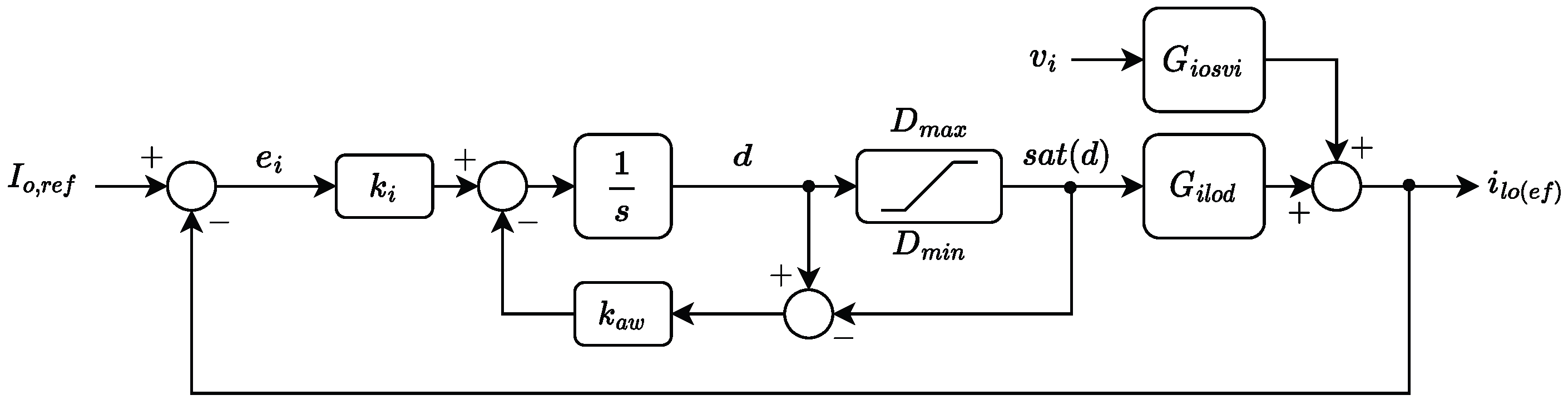
2.6. Transient-State Analysis
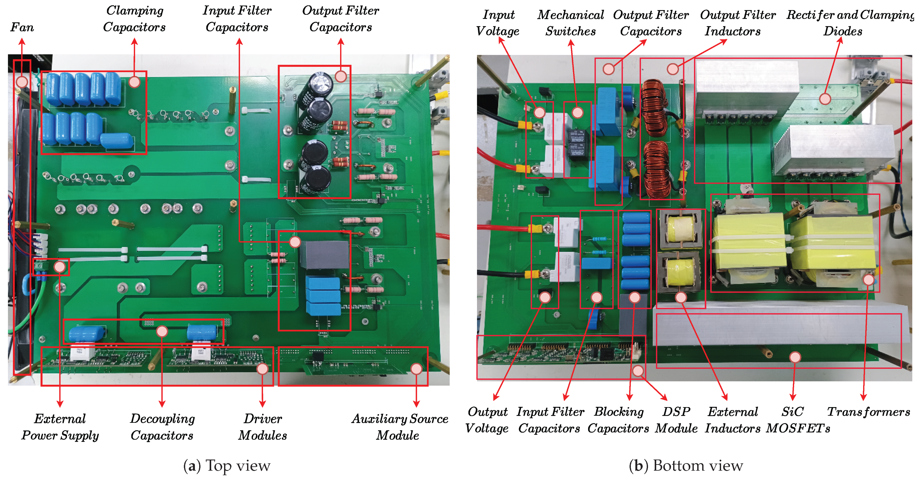
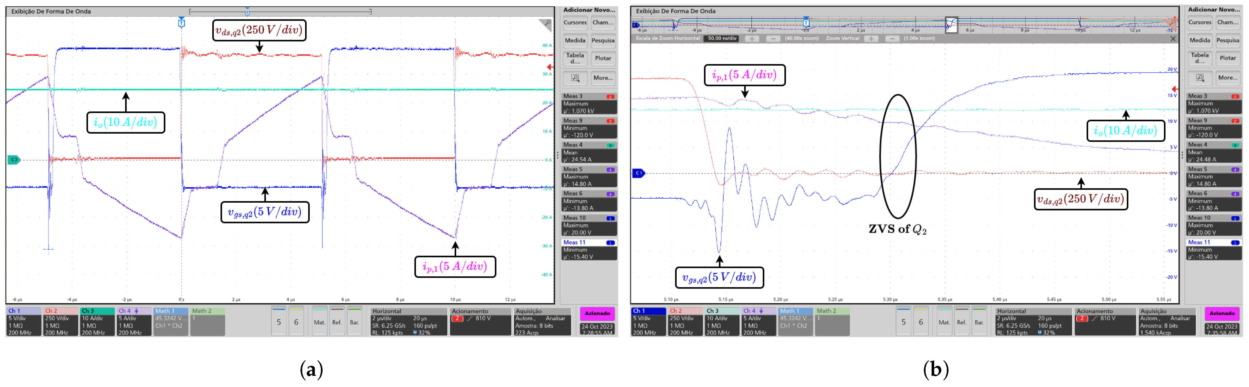
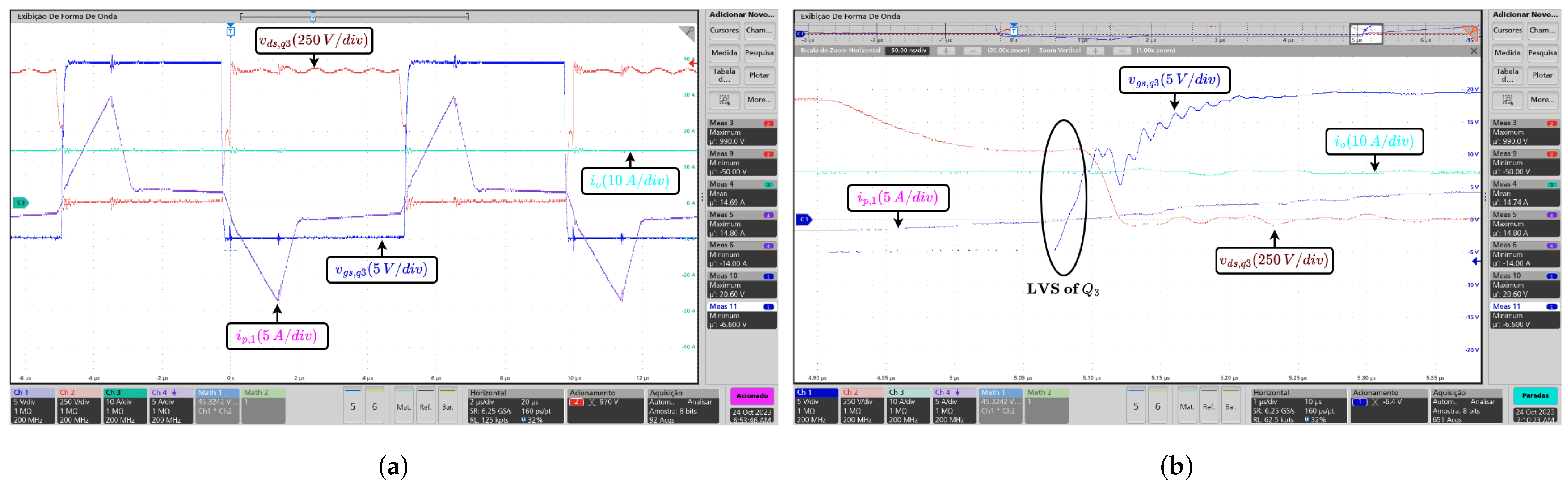
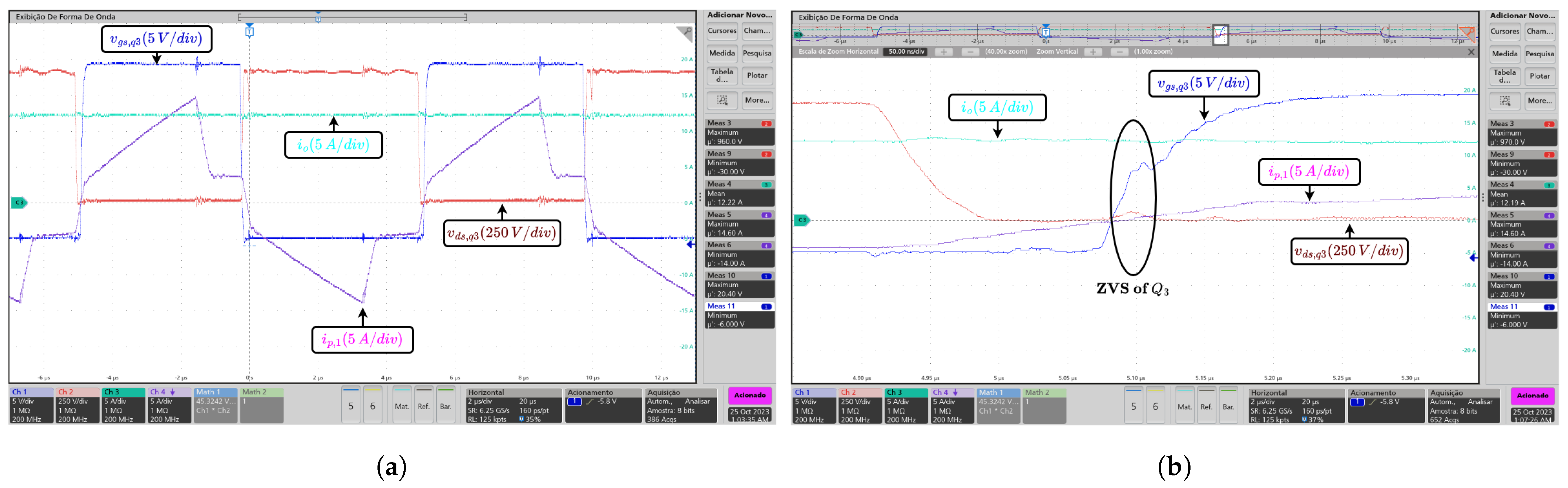
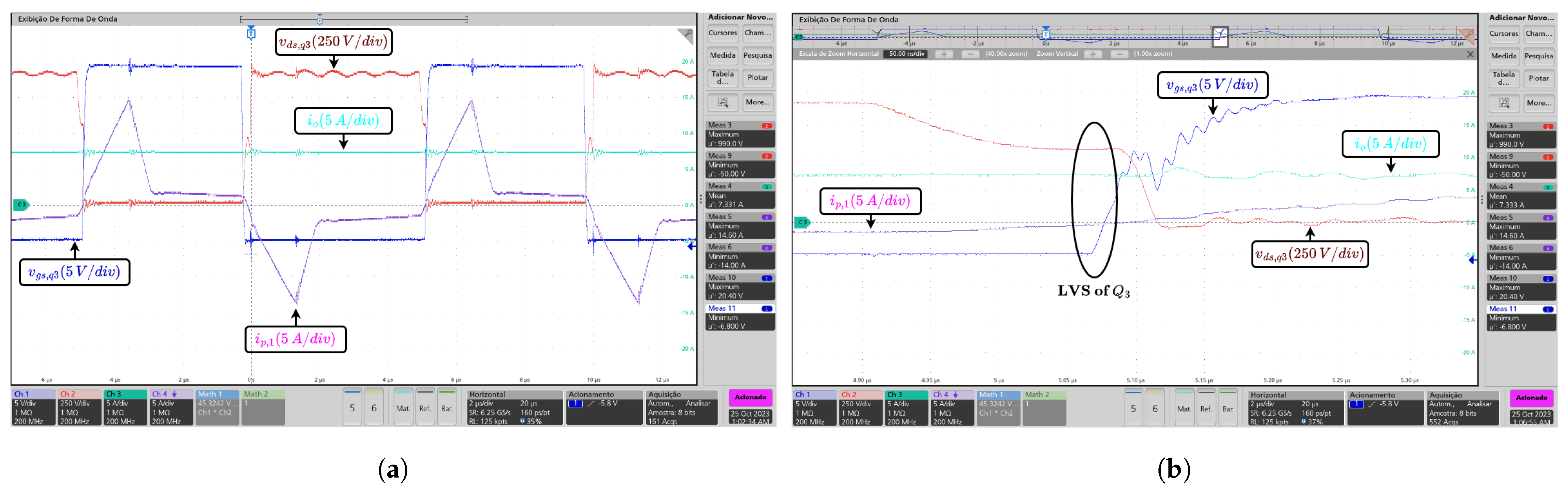
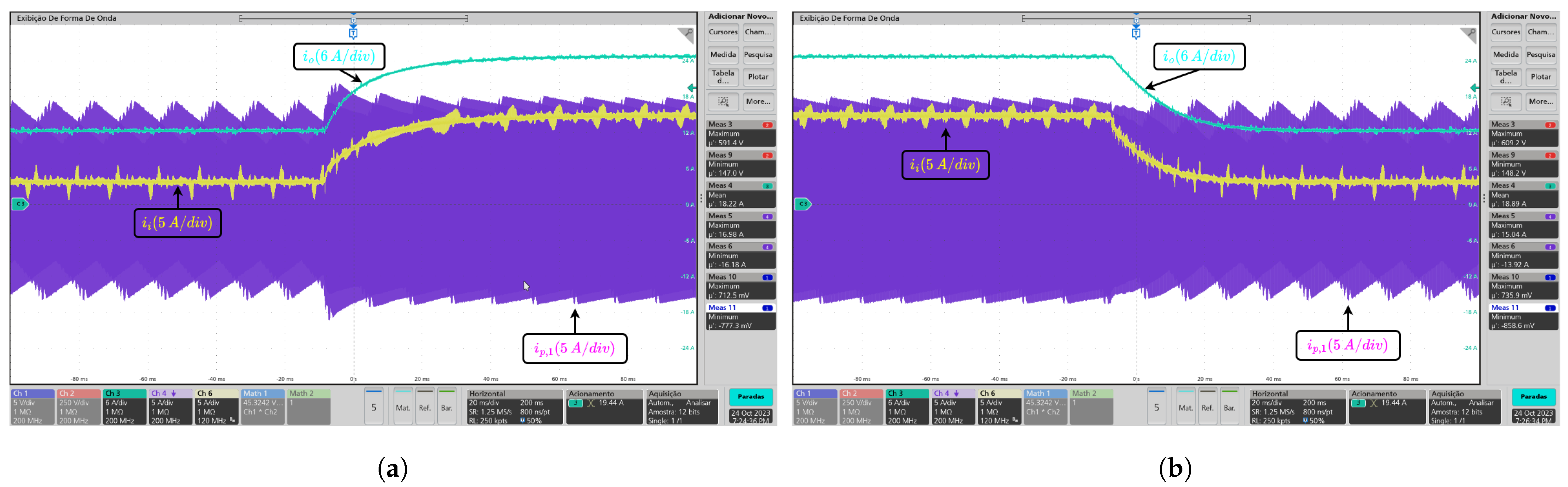
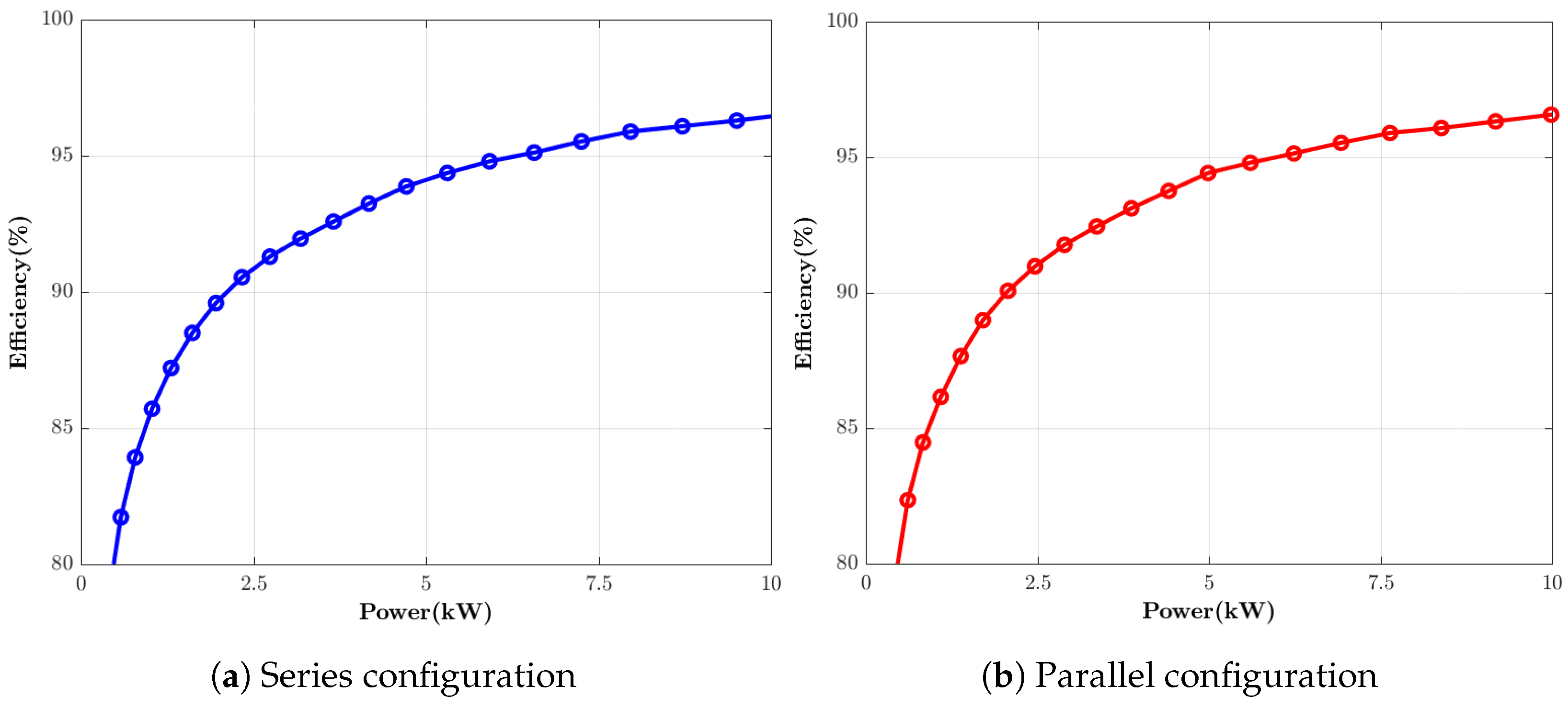
The dynamic model is obtained from the average model. From the principle of charge balance and volt-second balance, the large signal average model is given by:
d i l o ( e f ) ( t ) d t T s = ( 2 v c c ( e f ) ( t ) v c o ( e f ) ( t ) ) d e ( t ) ( v c o ( e f ) ( t ) v c c ( e f ) ( t ) ) d e ( t ) 0.5 L o ( e f ) ,
d v c c ( e f ) ( t ) d t T s = i l o ( e f ) ( t ) ( ε ( t ) d e ( t ) T s ( d e ( t ) T s + t 5 8 ( t ) ) ) C c ( e f ) T s .
where d e ( t ) = 0.5 d e ( t ) . From (50) and (51), the variables are defined as x i ( t ) = X i + x ˜ i , where X i is the average value and x ˜ i is the small signal disturbance. Then, the small signal average model can be expressed as follows:
L o ( e f ) d i ˜ l o ( e f ) ( t ) d t = γ v c c v ˜ c c ( e f ) + γ d e d ˜ e v ˜ c o ( e f ) ,
C c ( e f ) d v ˜ c c ( e f ) ( t ) d t = λ i l o i ˜ l o ( e f ) + λ v c c v ˜ c c ( e f ) + λ d e d ˜ e + λ v i v ˜ i .
where λ v i = I l o ( e f ) V i 1 { I l o n ( e f ) ( 1 V c n ( e f ) ) 2 8 V c n ( e f ) 2 D e 2 I l o n ( e f ) 1 } , γ d e = 2 V c c ( e f ) , λ i l o = 2 D e 1 + 2 I l o n ( e f ) V c n ( e f ) 1 ( 1 V c n ( e f ) ) 1 , λ d e = I l o ( e f ) { 16 ( 0.5 V c n ( e f ) ) V c n ( e f ) D e I l o n ( e f ) 1 + 2 } , λ v c c = I l o ( e f ) V c n ( e f ) V c c ( e f ) 1 { 8 ( 0.5 2 V c n ( e f ) ) D e 2 I l o n ( e f ) 1 I l o n ( e f ) ( 1 2 V c n ( e f ) ) V c n ( e f ) 2 ( 1 V c n ( e f ) ) 2 } , γ v c c = 1 + 2 D e , and λ v i = I l o ( e f ) V i 1 { I l o n ( e f ) ( 1 V c n ( e f ) ) 2 8 V c n ( e f ) 2 D e 2 I l o n ( e f ) 1 } .
Since D T s = t 0 1 + t 8 10 , the small signal average model of the control variable is obtained as follows:
d ˜ = δ i l o i ˜ l o ( e f ) + δ v c c v ˜ c c ( e f ) + δ d e d ˜ e δ v i v ˜ i
where δ v c c = V c n ( e f ) V c c ( e f ) 1 { 2 D e + I l o n ( e f ) ( 1 V c n ( e f ) ) 2 } , δ i l o = I l o n ( e f ) I l o ( e f ) 1 ( 1 V c n ( e f ) ) 1 , δ d e = 2 V c n ( e f ) , and δ v i = V i 1 ( 2 D e V c n ( e f ) + I l o n ( e f ) ( 1 V c n ( e f ) ) 2 ) .
From (52) to (54), the small signal average model in the Laplace domain is expressed as follows:
Ψ i l o i ˜ l o ( e f ) ( s ) = Ψ d d ˜ ( s ) + Ψ v i v ˜ i ( s ) Ψ v c o v ˜ c o ( e f ) ( s ) .
where Ψ i l o = ( L o ( e f ) C c ( e f ) δ d e ) s 2 + { L o ( e f ) ( λ d e δ v c c λ v c c δ d e ) + C c ( e f ) ( γ d e δ i l o ) } s + λ d e γ v c c δ i l o + λ i l o γ d e δ v c c λ v c c γ d e δ i l o λ i l o γ v c c δ d e , Ψ v c o = ( C c δ d e ) s + λ d e δ v c c λ v c c δ d e , Ψ d = ( C c ( e f ) γ d e ) s + λ d e γ v c c λ v c c γ d e , and Ψ v i = ( C c ( e f ) γ d e δ v i ) s + λ d e γ v c c δ v i + λ v i γ d e δ v c c λ v c c γ d e δ v i λ v i γ v c c δ d e .
Considering an output impedance disturbance z ˜ o ( s ) = v ˜ o / i ˜ o , the small signal average model is restructured as follows:
i ˜ l o ( e f ) ( s ) = G i l o d d ˜ ( s ) + G i l o v i v ˜ i ( s ) .
where G i l o d = Ψ d Ψ z o ( Ψ i l o Ψ z o + Ψ v c o ) 1 , G i l o v i = Ψ v i Ψ z o ( Ψ i l o Ψ z o + Ψ v c o ) 1 , and Ψ z o = ( C o ( e f ) ) s + z ˜ o 1 ( s ) . Figure 6 shows the control block diagram used for the converter.

3. Results

A 10 kW reconfigurable PSFB converter prototype was designed and built according to Table 3. Figure 7 shows the photograph of the top and bottom views of the prototype, whose outer dimensions are 320 mm × 460 mm × 140 mm. Table 4 illustrates the main components employed in the prototype. The design of the prototype is based on efficiency, volume and cost for commercial purposes. Thus, SiC MOSFETs were used on the primary side switches in order to take advantage of their reduced switching and conduction losses. Low-voltage hyperfast diodes were used on the secondary side switches to reduce losses and costs. Sendust toroidal cores were used to reduce the size of the output filter inductors. Finally, N87 EE cores were used to reduce losses at high frequencies of the transformers and external inductors. In addition, for measuring the performance of the proposed reconfigurable PSFB converter, KEYSIGHT RP7952A is used as an input power supply, TEKTRONIX PA4000 as an input and output power analyzer, and TEKTRONIX MS046 to capture the experimental waveforms.
Figure 8 shows the test scheme of the prototype. High-voltage pre-charge circuit-based IGBTs were developed and used to manage the inrush current. EMI filter circuits were developed and used to suppress conducted EMI noise. An auxiliary source module-based DC–DC switching regulator IC was developed and employed to provide various voltage levels required by different components. Driver module-based Si8285 ICs were developed and used for driving SiC MOSFETs with safety features. Finally, a DSP module-based TMS320F280037C DSP core was developed and employed for signal conditioning, communication and implementation of digital control algorithms.
A set of resistive loads of 16 Ω and 64 Ω were used for experimental tests with parallel and series connection, respectively, in order to reach the nominal values of the prototype. In addition, a gate resistor of 10 Ω is built-in, and a dead time of 238 ns is configured in the Driver modules. In addition, an integral controller with k i = 6 and k a w = 10 is designed to control the output current i o . The integral controller has a gain margin of G M = 56.7 dB at 14 kHz and a phase margin of P M = 114 ° at 20 Hz under full load condition. Instead, a gain margin of G M = 27.9 dB at 4 kHz and a phase margin of P M = 124 ° at 80 Hz under half load condition is obtained.
The experimental tests are performed at different power and voltage levels. Figure 9 and Figure 10 show experimental waveforms in the leading and lagging legs under full load condition ( i o = 25 A) for the parallel connection case. As shown in Figure 9a and Figure 10a, the proposed reconfigurable PSFB converter regulates well the output current with D = 0.3859 . Moreover, as can be seen in Figure 9b and Figure 10b, the ZVS turn-on operation is achieved. Under half load condition ( i o = 15 A), the experimental waveforms in the lagging leg are shown in Figure 11. Figure 11a shows that the output current is regulated with D = 0.1625 . Furthermore, Figure 11b shows that the lagging leg fails to achieve the ZVS operation; however, the low voltage switching (LVS) operation is performed.
Figure 12 and Figure 13 show the waveforms in the leading and lagging legs under full load condition ( i o = 12.5 A) for the series connection case. In Figure 12 and Figure 13, it is shown that the output current is controlled with D = 0.3549 , and the ZVS turn-on operation is achieved. From Figure 14, it is shown that, under half load condition ( i o = 7.5 A), the output current is controlled with D = 0.1549 and the lagging leg achieves the LVS operation.
The experimental waveforms depicted in Figure 15 and Figure 16 illustrate the output current transients between the full load and half load conditions, and vice versa, for cases of series and parallel connection. As shown in Figure 15 and Figure 16, the control strategy enables the rapid adjustment of the output current.
Table 5 and Table 6 show the voltage measurements on the output filter capacitors v c o and the current measurements on the output filter inductors i l o of the prototype for the series and parallel configuration. As shown in Table 5 and Table 6, the designed prototype presents minimal current and voltage imbalance errors, which are caused by uncertainties in the parameters of the elements that constitute the primary and secondary sides. The error e is calculated as the relationship between the difference and the mean of the measurements.
Figure 17 shows the measured efficiency of the prototype for the series and parallel configuration. The measurement did not consider the external power supply or external circuits used in the test scheme. As shown in Figure 17, the prototype has a high efficiency in a wide load range, achieving 96.69% under full load conditions.

4. Conclusions

In this paper, a reconfigurable PSFB converter has been proposed and analyzed. Its topology is based on two traditional PSFB converters with CDD clamping circuits connected at their outputs by switches. SPDT mechanical switches enabled series and parallel reconfigurations on the secondary side. In addition, an exhaustive analysis of the clamping mechanism was carried out, in which the main electrical parameters, electrical stresses, design conditions, and a small signal dynamic model were derived. Compared to state-of-the-art solutions, the proposed reconfigurable PSFB converter allows the design of a compact structure and reduced costs, making it attractive for commercial applications. A commercial prototype of 10 kW was developed in the laboratory, achieving a power density of 0.485 W/cm3. The series and parallel configuration made it possible to change the nominal output voltage between 400 V and 800 V, enabling the operation of the converter over an output voltage wide range. The experimental results showed that the reconfigurable PSFB converter can achieve high efficiency under various load conditions, reaching 96.69% efficiency at full load.

Author Contributions

Conceptualization, J.B.B.Q.; methodology, J.B.B.Q.; formal analysis, J.B.B.Q.; investigation, J.B.B.Q.; writing—original draft preparation, J.B.B.Q.; writing—review and editing, visualization, supervision, project administration, J.B.B.Q., M.M., A.L.B. and J.M.d.S.R. All authors have read and agreed to the published version of the manuscript.

Funding

This research was funded by Conselho Nacional de Desenvolvimento Científico e Tecnológico (CNPq) grant number 145566/2019-6, regarding the public call CNPq 23/2018 of the Academic Doctorate Program for Innovation-DAI/Unesp.

Data Availability Statement

The original contributions presented in the study are included in the article, further inquiries can be directed to the corresponding author.

Conflicts of Interest

The authors declare no conflicts of interest.

References

  1. Agarwal, A.; Prabowo, Y.; Bhattacharya, S. Analysis and Design Considerations of Input Parallel Output Series-Phase Shifted Full Bridge Converter for a High-Voltage Capacitor Charging Power Supply System. IEEE Trans. Ind. Appl. 2023, 59, 6037–6050. [Google Scholar] [CrossRef]
  2. Lee, D.; Youn, H.; Kim, J. Development of Phase-Shift Full-Bridge Converter with Integrated Winding Planar Two-Transformer for LDC. IEEE Trans. Transp. Electrif. 2023, 9, 1215–1226. [Google Scholar] [CrossRef]
  3. Mukherjee, S.; Saha, S.; Chowdhury, S. Battery Integrated Three-Port Soft-Switched DC–DC PSFB Converter for SPV Applications. IEEE Access 2023, 11, 62472–62483. [Google Scholar] [CrossRef]
  4. Métayer, P.; Loeuillet, Q.; Wallart, F.; Buttay, C.; Dujic, D.; Dworakowski, P. Phase-Shifted Full Bridge DC–DC Converter for Photovoltaic MVDC Power Collection Networks. IEEE Access 2023, 11, 19039–19048. [Google Scholar] [CrossRef]
  5. Pei, Z.; Guo, D.; Cui, T.; Liu, C.; Kong, D.; Zhu, D.; Jiang, Y.; Chen, N. Phase-Shift Full-Bridge (PSFB) Converter Integrated Double-Inductor Rectifier with Separated Resonant Circuits (SRCs) for 800 V High-Power Electric Vehicles. IEEE J. Emerg. Selec. Top. Power Electron. 2024, 12, 269–282. [Google Scholar] [CrossRef]
  6. Sabate, J.; Vlatkovic, V.; Ridley, R.; Lee, F.; Cho, B. Design considerations for high-voltage high-power full-bridge zero-voltage-switched PWM converter. In Proceedings of the Fifth Annual Proceedings on Applied Power Electronics Conference and Exposition, Los Angeles, CA, USA, 11–16 March 1990; pp. 275–284. [Google Scholar]
  7. Sabate, J.; Vlatkovic, V.; Ridley, R.; Lee, F. High-voltage, high-power, ZVS, full-bridge PWM converter employing an active snubber. In Proceedings of the Sixth Annual Applied Power Electronics Conference and Exhibition, Dallas, TX, USA, 10–15 March 1991; pp. 158–163. [Google Scholar]
  8. Yungtack, J.; Jovanovic, M.; Yu-Ming, C. A new ZVS-PWM full-bridge converter. IEEE Trans. Power Electron. 2003, 18, 1122–1129. [Google Scholar] [CrossRef]
  9. Guo, Z.; Sha, D.; Liao, X.; Luo, J. Input-Series-Output-Parallel Phase-Shift Full-Bridge Derived DC–DC Converters with Auxiliary LC Networks to Achieve Wide Zero-Voltage Switching Range. IEEE Trans. Power Electron. 2014, 29, 5081–5086. [Google Scholar] [CrossRef]
  10. Safaee, A.; Jain, P.; Bakhshai, A. A ZVS Pulsewidth Modulation Full-Bridge Converter with a Low-RMS-Current Resonant Auxiliary Circuit. IEEE Trans. Power Electron. 2016, 31, 4031–4047. [Google Scholar] [CrossRef]
  11. Zhao, L.; Li, H.; Wu, X.; Zhang, J. An Improved Phase-Shifted Full-Bridge Converter with Wide-Range ZVS and Reduced Filter Requirement. IEEE Trans. Ind. Electron. 2018, 65, 2167–2176. [Google Scholar] [CrossRef]
  12. Yang, X.; Li, Y.; Gao, Z.; Xi, L.; Wen, J. Analysis and Design of Full-Bridge Converter with a Simple Passive Auxiliary Circuit Achieving Adaptive Peak Current for ZVS and Low Circulating Current. IEEE J. Emerg. Selec. Top. Power Electron. 2021, 9, 2051–2065. [Google Scholar] [CrossRef]
  13. Shi, Y.; Feng, L.; Li, Q.; Kang, J. High Power ZVZCS Phase Shift Full Bridge DC–DC Converter with High Current Reset Ability and No Extra Electrical Stress. IEEE Trans. Ind. Electron. 2022, 69, 12688–12697. [Google Scholar] [CrossRef]
  14. Liu, G.; Wang, B.; Liu, F.; Wang, X.; Guan, Y.; Wang, W.; Wang, Y.; Xu, D. An Improved Zero-Voltage and Zero-Current- Switching Phase-Shift Full-Bridge PWM Converter with Low Output Current Ripple. IEEE Trans. Power Electron. 2023, 38, 3419–3432. [Google Scholar] [CrossRef]
  15. Mishima, T.; Akamatsu, K.; Nakaoka, M. A High Frequency-Link Secondary-Side Phase-Shifted Full-Range Soft-Switching PWM DC–DC Converter with ZCS Active Rectifier for EV Battery Chargers. IEEE Trans. Power Electron. 2013, 28, 5758–5773. [Google Scholar] [CrossRef]
  16. Dudrik, J.; Pástor, M.; Lacko, M.; Žatkovič, R. Zero-Voltage and Zero-Current Switching PWM DC–DC Converter Using Controlled Secondary Rectifier With One Active Switch and Nondissipative Turn-Off Snubber. IEEE Trans. Power Electron. 2018, 33, 6012–6023. [Google Scholar] [CrossRef]
  17. Li, G.; Xia, J.; Wang, K.; Deng, Y.; He, X.; Wang, Y. Hybrid Modulation of Parallel-Series LLC Resonant Converter and Phase Shift Full-Bridge Converter for a Dual-Output DC–DC Converter. IEEE J. Emerg. Selec. Top. Power Electron. 2019, 7, 833–842. [Google Scholar] [CrossRef]
  18. Li, G.; Yang, D.; Zhou, B.; Liu, Y.; Zhang, H. Integration of Three-Phase LLC Resonant Converter and Full-Bridge Converter for Hybrid Modulated Multioutput Topology. IEEE J. Emerg. Selec. Top. Power Electron. 2022, 10, 5844–5856. [Google Scholar] [CrossRef]
  19. Kim, J.; Lee, I.; Moon, G. Integrated Dual Full-Bridge Converter with Current-Doubler Rectifier for EV Charger. IEEE Trans. Power Electron. 2016, 31, 942–951. [Google Scholar] [CrossRef]
  20. Kanamarlapudi, V.; Wang, B.; Kandasamy, N.; So, P. A New ZVS Full-Bridge DC–DC Converter for Battery Charging with Reduced Losses Over Full-Load Range. IEEE Trans. Ind. Appl. 2018, 54, 571–579. [Google Scholar] [CrossRef]
  21. Tran, D.; Vu, H.; Yu, S.; Choi, W. A Novel Soft-Switching Full-Bridge Converter with a Combination of a Secondary Switch and a Nondissipative Snubber. IEEE Trans. Power Electron. 2018, 33, 1440–1452. [Google Scholar] [CrossRef]
  22. Lim, C.; Jeong, Y.; Lee, M.; Yi, K.; Moon, G. Half-Bridge Integrated Phase-Shifted Full-Bridge Converter with High Efficiency Using Center-Tapped Clamp Circuit for Battery Charging Systems in Electric Vehicles. IEEE Trans. Power Electron. 2020, 35, 4934–4945. [Google Scholar] [CrossRef]
  23. Jeong, H.; Lim, C. Hybrid DC–DC Converter with Novel Clamp Circuit in Wide Range of High Output Voltage. IEEE Access 2024, 12, 7775–7785. [Google Scholar] [CrossRef]
  24. Lim, C.; Jeong, Y.; Moon, G. Phase-Shifted Full-Bridge DC–DC Converter with High Efficiency and High Power Density Using Center-Tapped Clamp Circuit for Battery Charging in Electric Vehicles. IEEE Trans. Power Electron. 2019, 34, 10945–10959. [Google Scholar] [CrossRef]
  25. Bakar, M.; Alam, M.; Majid, A.; Bertilsson, K. Dual-Mode Stable Performance Phase-Shifted Full-Bridge Converter for Wide-Input and Medium-Power Applications. IEEE Trans. Power Electron. 2021, 36, 6375–6388. [Google Scholar] [CrossRef]
  26. Bakar, M.; Alam, M.; Wårdemark, M.; Bertilsson, K. A 2 × 3 Reconfigurable Modes Wide Input Wide Output Range DC-DC Power Converter. IEEE Access 2021, 9, 44292–44303. [Google Scholar] [CrossRef]
  27. Lyu, D.; Soeiro, T.; Bauer, P. Design and Implementation of a Reconfigurable Phase Shift Full-Bridge Converter for Wide Voltage Range EV Charging Application. IEEE Trans. Transp. Electrific. 2023, 9, 1200–1214. [Google Scholar] [CrossRef]
  28. Benites, J.; Mezaroba, M.; Batschauer, A.; Ribeiro, J. A DC/DC Converter for 400 V and 800 V EVs Fast Charging Stations. In Proceedings of the IEEE 8th Southern Power Electronics Conference and 17th Brazilian Power Electronics Conference, Florianopolis, Brazil, 26 November 2023. [Google Scholar]
  29. Tang, L.; Jiang, H.; Zhong, X.; Qiu, G.; Mao, H.; Jiang, X.; Qi, X.; Du, C.; Peng, Q.; Liu, L.; et al. Investigation Into the Third Quadrant Characteristics of Silicon Carbide MOSFET. IEEE Trans. Power Electron. 2023, 38, 1155–1165. [Google Scholar] [CrossRef]
Figure 1. Circuit diagram of the proposed reconfigurable PSFB converter adapted from [28].
Energies 17 03483 g001
Figure 2. Equivalent circuit of the proposed reconfigurable PSFB converter.
Energies 17 03483 g002
Figure 3. Key waveforms of the equivalent circuit in Figure 2.
Energies 17 03483 g003
Figure 4. Operation modes of the equivalent circuit in Figure 2.
Energies 17 03483 g004
Figure 5. Relationship surfaces according to D and I l o n ( e f ) adapted from [28].
Energies 17 03483 g005
Figure 6. Control block diagram.
Energies 17 03483 g006
Figure 7. Prototype of the proposed reconfigurable PSFB converter.
Energies 17 03483 g007
Figure 8. Reconfigurable PSFB converter prototype test scheme.
Energies 17 03483 g008
Figure 9. Parallel connection case: experimental waveforms in the leading leg under full load condition. (a) Waveforms of the drain-source voltage v d s , q 2 and gate-source voltage v g s , q 2 of switch Q 2 , primary current i p , 1 , and output current i o . (b) ZVS waveforms.
Energies 17 03483 g009
Figure 10. Parallel connection case: Experimental waveforms in the lagging leg under full load condition. (a) Waveforms of the drain-source voltage v d s , q 3 and gate-source voltage v g s , q 3 of switch Q 3 , primary current i p , 1 , and output current i o . (b) ZVS waveforms.
Energies 17 03483 g010
Figure 11. Parallel connection case: Experimental waveforms in the lagging leg under half load condition. (a) Waveforms of the drain-source voltage v d s , q 3 and gate-source voltage v g s , q 3 of switch Q 3 , primary current i p , 1 , and output current i o . (b) LVS waveforms.
Energies 17 03483 g011
Figure 12. Series connection case: Experimental waveforms in the leading leg under full load condition. (a) Waveforms of the drain-source voltage v d s , q 2 and gate-source voltage v g s , q 2 of switch Q 2 , primary current i p , 1 , and output current i o . (b) ZVS waveforms.
Energies 17 03483 g012
Figure 13. Series connection case: Experimental waveforms in the lagging leg under full load condition. (a) Waveforms of the drain-source voltage v d s , q 3 and gate-source voltage v g s , q 3 of switch Q 3 , primary current i p , 1 , and output current i o . (b) ZVS waveforms.
Energies 17 03483 g013
Figure 14. Series connection case: Experimental waveforms in the lagging leg under half load condition. (a) Waveforms of the drain-source voltage v d s , q 3 and gate-source voltage v g s , q 3 of switch Q 3 , primary current i p , 1 , and output current i o . (b) LVS waveforms.
Energies 17 03483 g014
Figure 15. Parallel connection case: Experimental waveforms for a load transient. (a) Output current from 12.5 A to 25 A. (b) Output current from 25 A to 12.5 A.
Energies 17 03483 g015
Figure 16. Series connection case: Experimental waveforms for a load transient. (a) Output current from 6.25 A to 12.5 A. (b) Output current from 12.5 A to 6.25 A.
Energies 17 03483 g016
Figure 17. Measured efficiency of the prototype.
Energies 17 03483 g017
Table 1. Equivalent circuit parameters.
S s , S p L lk ( ef ) L m ( ef ) C b ( ef ) i p ( ef ) i lm ( ef )
- 0.5 L l k 0.5 L m 2 C b 2 i p 2 i l m
S s , S p n ef C c ( ef ) L o ( ef ) C o ( ef ) i s ( ef ) i d ( ef ) i dc ( ef ) i cc ( ef ) v cc ( ef ) i lo ( ef )
series1, 0 2 n 0.5 C c 2 L o 0.5 C o i s i d i d c i c c 2 v c c i l o
parallel0, 1n 2 C c 0.5 L o 2 C o 2 i s 2 i d 2 i d c 2 i c c v c c 2 i l o
Table 2. Current stresses in the components of the equivalent circuit in Figure 2.
VariableValue
Q I q ( e f ) , 1 t h , l a g , r m s n e f I l o ( e f ) 1 3 T s ( ζ b 3 ζ a 3 ζ b ζ a t 0 1 + ζ a 3 + ζ d 3 ζ a + ζ d t 8 10 )
I q ( e f ) , 1 t h , l e a d , r m s n e f I l o ( e f ) 1 3 T s ( ζ b 3 ζ a 3 ζ b ζ a t 0 1 + ζ b 3 ζ c 3 ζ b ζ c t 1 4 + ζ c 3 ζ d 3 ζ c ζ d t 4 5 + 3 ζ d 2 t 5 8 + ζ a 3 + ζ d 3 ζ a + ζ d t 8 10 )
I q ( e f ) , 3 t h , l a g , r m s n e f I l o ( e f ) 1 3 T s ( ζ b 3 ζ c 3 ζ b ζ c t 1 4 + ζ c 3 ζ d 3 ζ c ζ d t 4 5 + 3 ζ d 2 t 5 8 )
I q ( e f ) , 3 t h , l e a d , r m s 0
D I d ( e f ) , u p , a v g I l o ( e f ) 1 2 T s ( 2 D e T s + t 4 5 + t 8 10 )
I d ( e f ) , u p , r m s I l o ( e f ) 1 T s ( D e T s + t 4 5 3 + t 8 10 3 )
I d ( e f ) , d w , a v g 0.5 I l o ( e f )
I d ( e f ) , d w , r m s I l o ( e f ) 1 T s ( 0.5 T s + ε 2 D e T s 3 + t 4 5 3 + t 5 8 + t 8 10 3 )
D c I d c 1 ( e f ) , a v g ε I l o ( e f ) D e
I d c 1 ( e f ) , r m s ε I l o ( e f ) 2 D e 3
I d c 2 ( e f ) , a v g ε I l o ( e f ) D e
I d c 2 ( e f ) , r m s I l o ( e f ) 2 T s ( t 4 5 3 + t 5 8 + t 8 10 3 )
C c I c c ( e f ) , r m s I l o ( e f ) 2 T s ( ε 2 D e T s 3 + t 4 5 3 + t 5 8 + t 8 10 3 )
C b I c b ( e f ) , r m s n e f I l o ( e f ) 2 3 T s ( ζ b 3 ζ a 3 ζ b ζ a t 0 1 + ζ b 3 ζ c 3 ζ b ζ c t 1 4 + ζ c 3 ζ d 3 ζ c ζ d t 4 5 + 3 ζ d 2 t 5 8 + ζ a 3 + ζ d 3 ζ a + ζ d t 8 10 )
T I p ( e f ) , r m s n e f I l o ( e f ) 2 3 T s ( ζ b 3 ζ a 3 ζ b ζ a t 0 1 + ζ b 3 ζ c 3 ζ b ζ c t 1 4 + ζ c 3 ζ d 3 ζ c ζ d t 4 5 + 3 ζ d 2 t 5 8 + ζ a 3 + ζ d 3 ζ a + ζ d t 8 10 )
I s ( e f ) , r m s I l o ( e f ) 1 T s ( 0.5 T s + ( ε 2 3 + 1 ) D e T s + 2 t 4 5 3 + t 5 8 + 2 t 8 10 3 )
Table 3. Parameters of the reconfigurable PSFB converter prototype.
ParameterSymbolValue
Input voltage V i 900 V
Rated output voltage V o 400 V/800 V
Rated output current I o 25 A/12.5 A
Rated output power P o 10 kW
Switching frequency f s 100 kHz
Maximum output current ripple Δ i l o , m a x 4.5 A
Maximum input voltage ripple Δ v c i , m a x 9 V
Maximum output voltage ripple Δ v c o , m a x 5 V
Maximum blocking voltage ripple Δ v c b , m a x 9 V
Transformer turns ration0.6
Leakage Inductance L l k 27.4 μ H
Magnetizing Inductance L m 640 μ H
Table 4. Main devices using in the prototype.
ComponentSymbolDescription
MOSFET Q 1 Q 4 NTHL080N120SC1 (1200 V, 22 A, 110 m Ω , C o s s = 80 pF)
Rectifier Diode D 1 D 4 VS-ETX3007-M3 (650 V, 30 A, V f = 1.6 V, t r r = 35 ns)
Clamping Diode D c 1 VS-15ETH03-M3 (300 V, 15 A, V f = 0.85 V, t r r = 32 ns)
D c 2 VS-30ETH06-M3 (600 V, 30 A, V f = 1.34 V, t r r = 23 ns)
Core: 2 × MMT140EE6527
TransformerT L m = 641 μ H/665.3 μ H, L l k g = 8.4 μ H/8.83 μ H
N p : N s 1 : N s 2 = 20 : 6 : 6
External Inductor L e x t Core: 1 × MMT140EE4220
L = 18.37 μ H/18.6 μ H
Output Filter Inductor L o Core: 1 × MMTS60T5715
L = 237.8 μ H/342.51 μ H
Input Filter Capacitor C i MP F863H KEMET (10 μ F, 1200 V) +
MP B32774 TDK (4 × 1.5 μ F, 1200 V)+
B43840-A9477 Epcos (2/3 × 470 μ F, 400 V)
Blocking Capacitor C b MP B32614 TDK (3 × 1 μ F, 630 V)
Clamping Capacitor C c MP B32614 TDK (5 × 2.2 μ F, 630 V)
Output Filter Capacitor C o MP B32776 TDK (12 μ F, 1000 V)+
MP B32774 TDK (1.5 μ F, 1200 V)+
B43845-A5227 Epcos (1/2 × 220 μ F, 450 V)
Table 5. Voltage and current measurements of the prototype for the series configuration.
i o , ref i lo , 1 i lo , 2 e ilo v co , 1 v co , 2 v o e vco
1.5 A1.552 A1.484 A4.48%44.066 V40.984 V85.050 V7.25%
3 A2.999 A2.961 A1.27%85.817 V81.617 V167.434 V5.01%
4.5 A4.542 A4.466 A1.68%128.305 V123.881 V252.186 V3.51%
6 A6.037 A5.932 A1.75%171.706 V166.629 V338.335 V3.01%
7.5 A7.532 A7.481 A0.67%213.501 V210.126 V423.627 V1.59%
9 A9.077 A8.979 A1.08%256.547 V254.688 V511.235 V0.72%
10.5 A10.583 A10.476 A1.01%298.008 V297.991 V595.999 V0.01%
12.5 A12.576A12.498 A0.62%357.791 V356.973 V714.764 V0.23%
Table 6. Voltage and current measurements of the prototype for the parallel configuration.
i o , ref i lo , 1 i lo , 2 i o e ilo v co , 1 v co , 2 e vco
3 A1.567 A1.449 A3.016 A7.82%45.241 V44.744 V1.11%
6 A3.073 A2.917 A5.99 A5.21%88.545 V88.026 V0.58%
9 A4.671 A4.335 A9.01 A7.46%133.171 V133.411 V0.18%
12 A6.212 A5.765 A11.977 A7.46%177.872 V178.241 V0.21%
15 A7.721 A7.224 A14.945 A6.65%222.922 V223.813 V0.39%
18 A9.304 A8.703 A18.007 A6.67%268.946 V269.741 V0.29%
21 A10.836 A10.138 A20.974 A6.65%312.028 V314.963 V0.93%
25 A13.077 A11.926 A25.003 A9.21%374.269 V375.429 V0.31%
Disclaimer/Publisher’s Note: The statements, opinions and data contained in all publications are solely those of the individual author(s) and contributor(s) and not of MDPI and/or the editor(s). MDPI and/or the editor(s) disclaim responsibility for any injury to people or property resulting from any ideas, methods, instructions or products referred to in the content.

