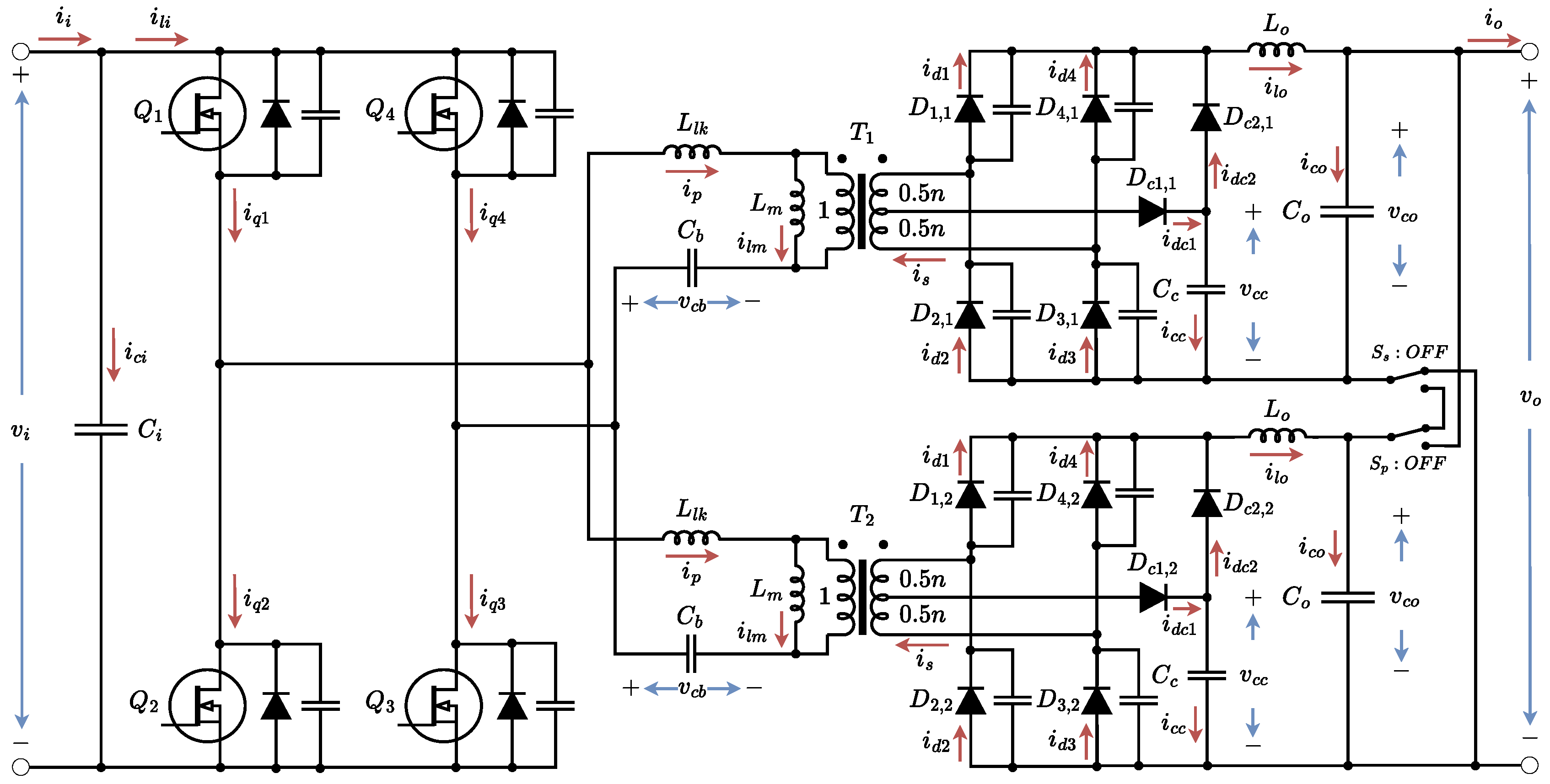
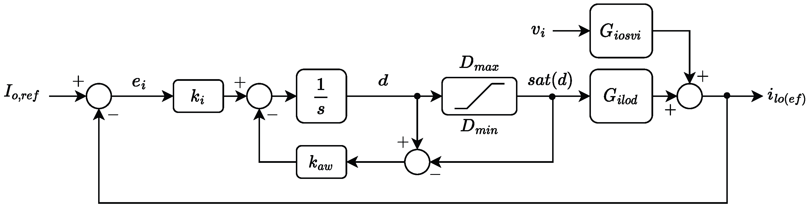
2.2. Operation Analysis
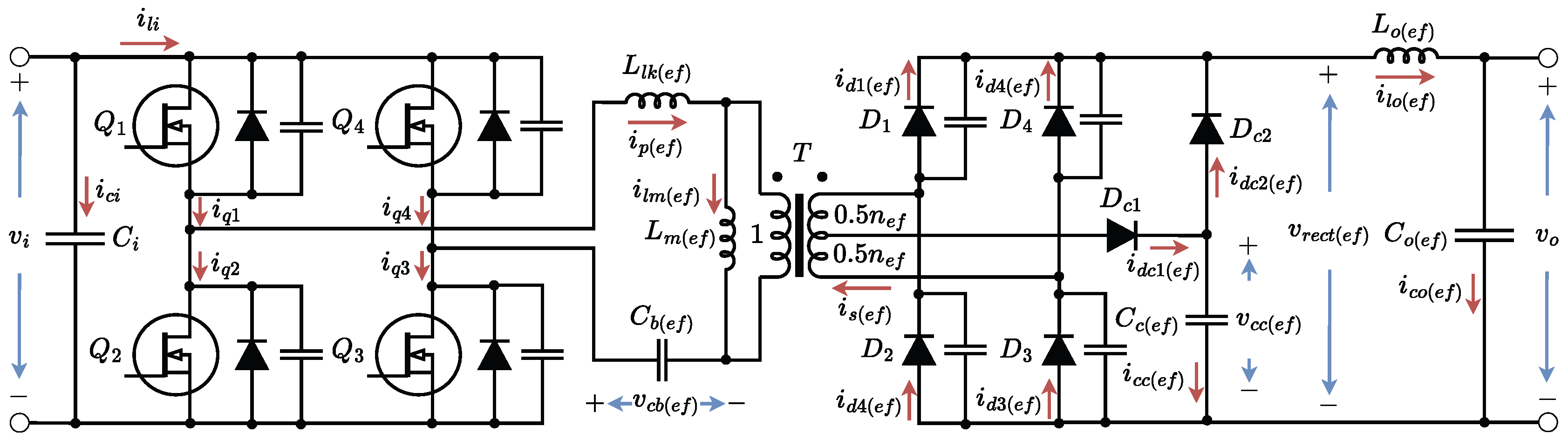
The proposed reconfigurable PSFB converter can be seen as equivalent to a traditional PSFB converter with a CDD clamp circuit, being either the series or parallel connection configuration. The equivalent circuit of the proposed reconfigurable PSFB converter is shown in
Figure 2.
Table 1 lists the equivalent circuit parameters.
The control method is pulse-width modulation with phase-shift.
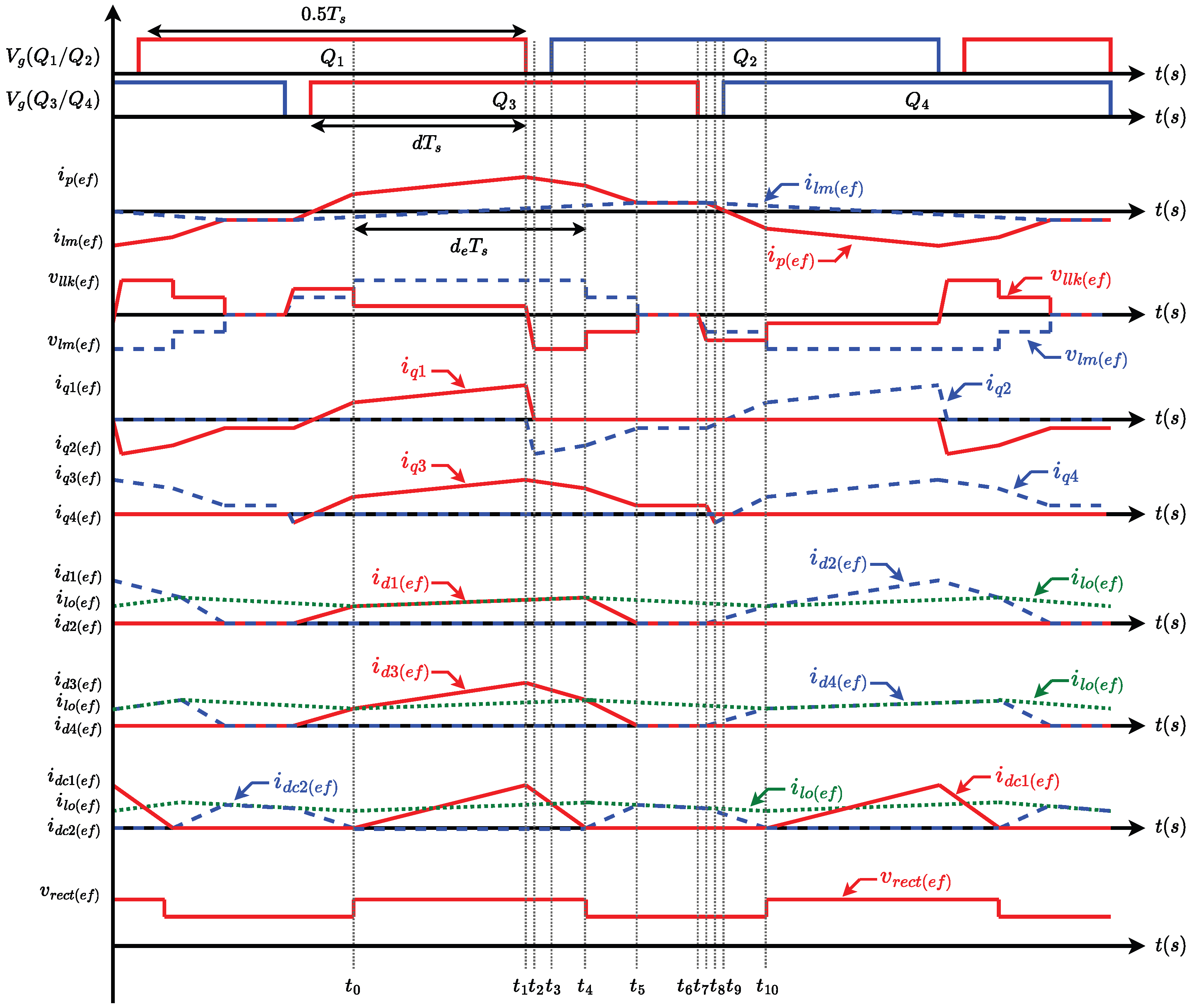
Figure 3 shows the key waveforms of the equivalent circuit in
Figure 2. Each switching period
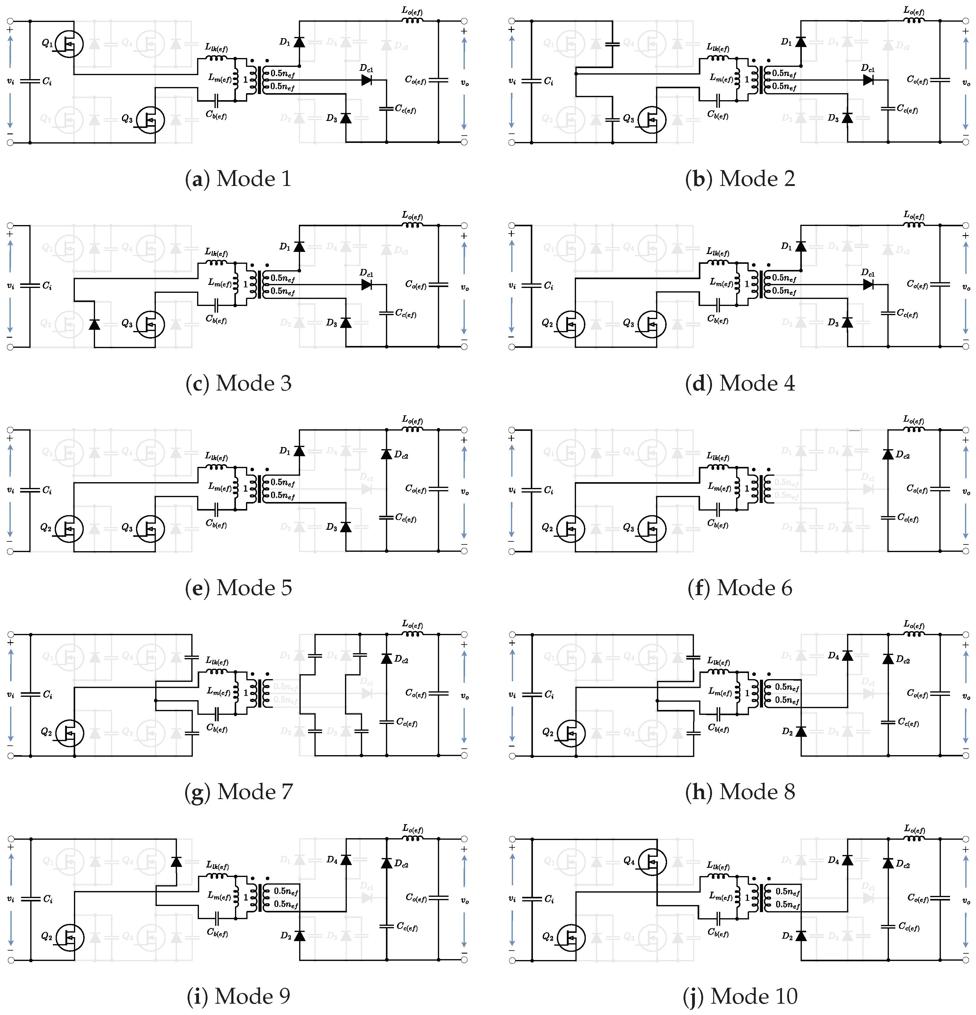
is divided into two half-cycles, where each half-cycle is subdivided into ten operation modes. Since the operation modes are symmetrical, only one half-cycle is analyzed. The equivalent operation circuits are shown in
Figure 4. In order to analyze the operation modes, the following assumptions are made to simplify analysis: (1) The clamping capacitance
is sufficiently large to be treated as a constant voltage source. (2) The output filter inductance
is sufficiently large to be treated as a constant current source. (3) The blocking capacitance
is sufficiently large to be treated as a negligible constant voltage source. (4) The transformer is ideal, except for its leakage inductance
and magnetizing inductance
. (5) MOSFETs
–
are identical and ideal, except for their output parasitic capacitances
and body diodes. (6) The rectifier diodes
–
are identical and ideal, except for their junction capacitances. (7) The clamping diodes
–
are identical and ideal. (8) An external inductor
is included into the leakage inductor
. In addition, the following notations are described:
and
are the MOSFET voltage and current,
and
are the leakage inductor voltage and current,
and
are the transformer magnetizing voltage and current,
is the rectifier diode current,
is the clamping diode current,
and
are the clamping capacitor voltage and current,
is the rectifier output voltage,
is the blocking capacitor voltage, and
and
are the output filter inductor voltage and current,
is the effective duty cycle and
d is the duty cycle.
Mode 1 (
): This mode starts when
is turned off and
is turned on. During this interval, the energy is transferred from the input to the output. In addition,
is clamped to
,
is
,
is
and
is
. Thus,
,
and
are given as follows:
Mode 2 (
): This mode begins when
is turned off. During this interval, the parasitic capacitances of
and
are charged and discharged by
. As a result,
and
are expressed as follows:
Mode 3 (
): This mode starts when the body diode of
is turned on. Here, the freewheel period is started. In addition, the energy is transferred from the primary side to the secondary side. Furthermore,
is
. Thus,
is given as follows:
Mode 4 (
): This mode begins when
is turned on with ZVS. During this interval,
begins to operate in the third quadrant [
29].
Mode 5 (
): This mode starts when
is turned on and
is turned off. During this interval,
is clamped to
,
is
,
is
and
is
. As a result,
,
and
are expressed as follows:
Mode 6 (
): This mode begins when
reaches
. During this interval, the turn-off process of the rectifier diodes is initiated, where
is clamped to
. Here, the stored energy in
is transferred to the output. In addition,
and
are 0. Thus,
,
and
are given as follows:
Mode 7 (
): This mode starts when
is turned off. During this interval, the parasitic capacitances of
,
and
–
are charged and discharged. Here,
participates in the charge and discharge resonance process. Thus,
and
are expressed as follows:
Mode 8 (
): This mode begins when
and
are turned on. During this interval, the output parasitic capacitances of
and
are charged and discharged by
. In addition,
is
. As a result,
,
,
,
and
are given as follows:
where
and
.
Mode 9 (
): This mode starts when the body diode of
is turned on. Here, the freewheel period is ended. In addition, a portion of the stored energy is returned to the input. Furthermore,
is
. Thus,
is given as follows:
Mode 10 (): This mode begins when is turned on with ZVS. During this interval, begins to operate in the third quadrant. In addition, the energy is transferred from the input to the output.
2.3. Steady-State Analysis
In order to simplify the mathematical analysis, the time intervals of the modes that describe the switching processes of the primary-side switches are neglected.
Since
is 0, then from (
7) to (
11) the time interval
can be obtained as follows:
where
is the normalized output filter inductor current,
is the normalized clamping capacitor voltage, and
is the inductance factor.
From (
1) to (
3), (
18) to (
20), and since
is 0, the time interval
can be expressed as follows:
As
, from (
1) to (
3) and (
6) to (
9), the time intervals
and
can be obtained as follows:
From (
21) to (
24), the time interval
can be expressed as follows:
From (
3), (
9), (
12) and (
19), and by using the capacitor charge balance principle, the clamping capacitor voltage can be obtained as follows:
where
,
,
,
,
, and
. The unique real solution of Equation (
26) is obtained considering that
. Thus, the clamping capacitor voltage is obtained by solving (
26) and calculated as
.
Then, by using the inductor volt-second balance principle, the voltage gain, defined as
, is obtained as follows:
where
is the normalized voltage gain. Thus, the voltage gain is calculated as
.
Finally, as
, the effective duty cycle can be expressed as follows:
The relationship surfaces of
and
according to
D and
are illustrated in
Figure 5. An increase in
reduces the available operating range of
and
to their limiting value of 0.0656. Conversely, a decrease in
increases the available operating range. However, smaller values and narrower variations of
D are required to guarantee a wide operating range of the converter.


 ,
, 


