Article

A Hybrid Beat Frequency Oscillation Suppression Strategy for DC Microgrids †

School of Mechanical, Electrical and Manufacturing Engineering, Loughborough University, Loughborough LE11 3LD, UK
*
Author to whom correspondence should be addressed.
This paper is an extended version of our paper published in 14th IEEE International Symposium on Power Electronics for Distributed Generation Systems (PEDG), Shanghai, China, titled “Beat Frequency Oscillation Analysis for a DC Microgrid with Multiple Boost Converters,” presented in 2023.
Energies 2024, 17(14), 3513; https://doi.org/10.3390/en17143513
Submission received: 15 June 2024 / Revised: 11 July 2024 / Accepted: 13 July 2024 / Published: 17 July 2024
(This article belongs to the Special Issue Advanced Switching Power Converters: Topologies, Control, and Devices)

Abstract

:
In DC microgrids, parallel-connected power converters are commonly used to integrate distributed energy sources. However, interactions of power switching noises among these power converters could lead to large low-frequency beat frequency oscillations under certain conditions, which degrades system performance and reliability, especially for DC microgrids with parallel connected Boost converters. In this research, the output impedance model for multiple parallel-connected Boost converters is developed for beat frequency oscillation analysis, and then a hybrid method is proposed to address this issue. The proposed method includes separated switching frequency channels and additional line inductors. Experimental results validate the effectiveness of the proposed method.

1. Introduction

With recent advancements in distributed generations (DGs), microgrids have become a popular solution for integrating DGs into the utility grids [1,2,3]. DC microgrids have advantages over AC systems, including reduction of AC–DC conversion stages, simplified control and no reactive power [4,5], and have gained an increasing research interest over the past few years.
A typical DC microgrid configuration is illustrated in Figure 1. In general, a DC microgrid comprises DGs, energy storage systems (ESSs) and local loads connected to a common DC bus via power converters. These power converters are essential in a microgrid for efficient, reliable and flexible operation, thus enhancing the system’s overall performance [6,7]. However, those power converters are usually feedback-controlled, and when they are parallel-connected, the interactions between them could introduce issues such as system instability, power quality, and beat frequency oscillations [8,9,10,11,12].
Beat frequency oscillations occur when multiple parallel-connected power converters operate at different power switching frequencies. The output voltage ripples caused by power devices switching in one power converter may pass into the output terminal of other power converters as a perturbation via the common DC bus. When these ripples with different frequencies are superimposed, they can interact and produce low frequency sideband components. This phenomenon is called beat frequency oscillation where the perturbation frequency is equal to the switching frequency difference of these power converters.
For feedback-controlled power converters, the control loop is usually designed to have high gains in a low-frequency region; therefore, the impact of the perturbation can be significant under certain conditions [11,12]. In [11], a large beat frequency oscillation of the DC bus voltage is observed when two voltage-mode controlled Buck converters operate with slightly different switching frequencies. In [12], low-frequency oscillations appear in the output voltage when the frequency of the perturbation in the voltage control loop is close to the switching frequency. It shows that the beat frequency oscillation can affect the performance and stability of the DC microgrid.
To alleviate this perturbation, switching frequency synchronization has been proposed for microgrid applications [13,14]. Ideally, beat frequency oscillation will not occur if two power converters operate at the same switching frequency. For micro-processor-controlled power converters, the switching frequency is determined by the switching frequency setting and the reference oscillator clock of the microprocessor. Switching frequencies of all power converters could be synchronized to be strictly the same by connecting all microcontrollers to the same external clock, so that the beat frequency oscillation could be solved. However, this method has limitations, and is not suitable for distributed controlled microgrid applications.
For two power converters without the external clock link, even if the switching frequency is set to the same value, slight differences in the actual switching frequencies of these two power converters can still occur due to the hardware tolerance of the different reference oscillator clocks [15]. It will cause very low frequency, but large amplitude beat frequency oscillations, which are difficult to be removed by low-pass filters between the power converter output terminal and the common DC bus.
To analyze beat frequency perturbations, an effective beat frequency oscillation analysis model based on the DC microgrid structure is often required. When the low-frequency component of the oscillations becomes the main concern, traditional average and linearized impedance models are not suitable due to the fact that they ignore the inherent nonlinear nature of the power converter [16]. Therefore, various models considering the nonlinearities of power converters have been proposed for beat frequency oscillation analysis in various applications.
In [17], a crossed frequency output impedance matrix model for Buck converters is introduced to analyze and estimate the beat frequency oscillations. In [18], a small-signal model for a dual-bridge series resonant converter is proposed for analysis on the dynamic characteristic at a low and medium frequency band. In [19], a harmonic state space model is developed for two cascaded voltage regulators in a power system to study the root cause of beat frequency oscillations. Beat frequency oscillation issues have also been investigated in two-stage AC/DC/AC motor drives [20], and wireless power transfers [21].
Several suggestions have been made to reduce the beat frequency oscillations for two parallel-connected Buck converters [12], which include setting switching frequencies of two Buck converters far away from each other, using an output capacitor with low equivalent series resistance (ESR), and incorporating current chokes to increase high-frequency cable impedance.
However, little research has been conducted on beat frequency oscillations with Boost converters, which are commonly used in DC microgrid applications. Due to the discontinuous output current of Boost converters, the issue of beat frequency oscillations is more severe when a DC microgrid has multiple Boost converters. The effectiveness of the solutions proposed in [12] on Boost converters needs further study.
This research focuses on addressing beat frequency oscillations for DC microgrids with multiple Boost converters. Other power converters, such as resonant converters and AC/DC/AC converters, are beyond the scope of this study.
Two main contributions of the paper are:
(1)
It reviews the difference between Buck converters and Boost converters’ output voltage ripples, and provides a detailed beat frequency oscillation analysis model for parallel-connected Boost converters, which was not previously addressed in [12,17].
(2)
It proposes a hybrid method to reduce beat frequency oscillations. A detailed investigation was conducted to study the impacts of the switching frequency channel setting and line inductor selection. The effectiveness of the method was experimentally validated.
The rest of this paper is organized as follows: Section 2 presents the beat frequency oscillation analysis, including a review of Boost converters output voltage ripples, and the establishment of a small-signal model for multiple parallel-connected Boost converters. Then, the proposed hybrid method is explained in Section 3. Experimental results are presented in Section 4. The paper ends with conclusions in Section 5.

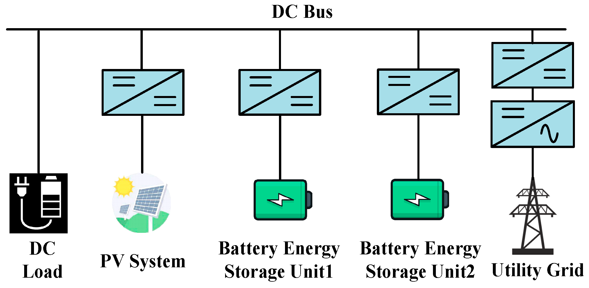
2. Beat Frequency Oscillation Analysis for Parallel Connected Boost Converters

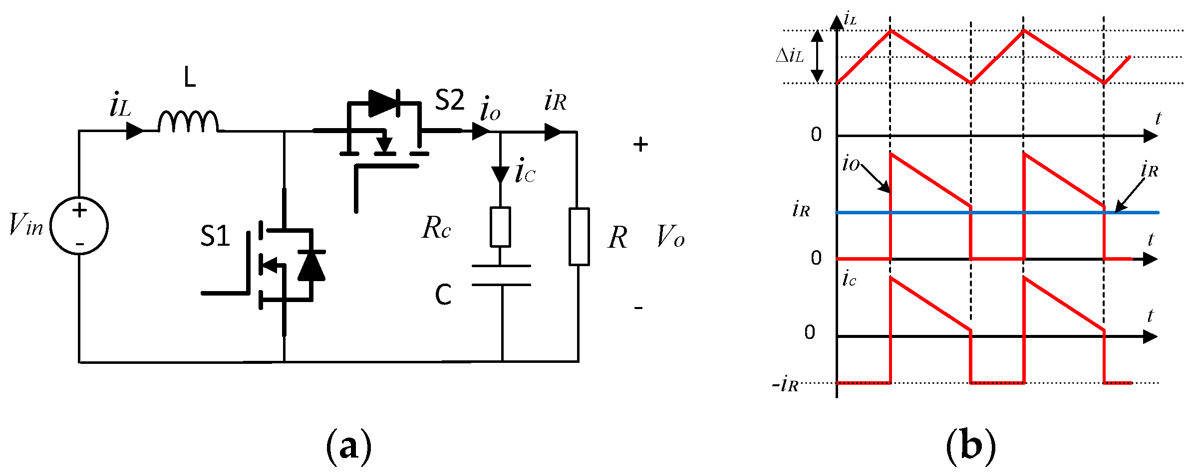
2.1. Reviewo of Buck Converters and Boost Converters Output Voltage Ripples

As mentioned in the introduction, for parallel-connected power converters, the switching frequency output voltage ripples of one power converter may pass into the output terminal of the other power converters via the common DC bus and introduce perturbations.
Figure 2 shows a bi-directional Buck converter and its current waveforms at a continuous current mode. The output voltage ripples are caused by the capacitor charging/discharging current i c , as shown in Figure 2b. The output voltage ripple Δ V o of a Buck converter can be calculated as:
Δ V o = Δ i L 8 f s C + R C Δ i L
where Δ i L is the amplitude of the inductor current ripple, f s is the power switching frequency, C is the capacitance of the output capacitor, and R C is the equivalent series resistance (ESR) of the capacitor C.
Equation (1) shows that for a Buck converter, the output voltage ripple is not dependent on the load and can be reduced by increasing the inductance L to reduce Δ i L .
Figure 3 shows a bi-directional Boost converter and its currents waveforms at a continuous current mode. The output current i O is discontinuous and has a large amplitude which depends on the load. The capacitor C charging/discharging current is the difference between the load current i R and i O ; therefore, it has a large amplitude Δ i c , as shown in Figure 2b. The output voltage ripple Δ V o of a Boost converter can be calculated as:
Δ V o = V o D R f s C + R C Δ i c
where R is the load resistance, D is the duty cycle, f s is the power switching frequency, C is the capacitance of the output capacitor, R C is the equivalent series resistance of the capacitor C, and Δ i c is the capacitor current ripple.
Equation (2) shows that the output voltage ripple of a Boost is much higher compared to a Buck converter with similar circuit parameters. This ripple is load-dependent, which means higher load currents lead to higher output voltage ripples. Also, the output voltage ripple only can be slightly reduced by increasing the inductance L.
Based on the above analysis, it is evident that a Boost converter could cause higher beat frequency oscillations than a Buck converter in a DC microgrid. This issue will be addressed in this research.

2.2. Closed Loop Output Impedance of Boost Converters

In this section, the output impedance model is construed to describe the output terminal characteristics of Boost converters using the modeling technique detailed in [12,17].
Figure 4 shows the block diagram of a bi-directional Boost converter with a double-loop droop controller. R is the load resistance. The current i o 2 is the external perturbation to the system and can be used for the Boost converter output impedance analysis. GADC is the gain for ADC, and GPWM is the gain for the PWM module. They can be simplified as G A D C 1 and G P W M 1 . Rd is the droop coefficient.
From Figure 4, the block diagram of the small-signal model for a closed-loop Boost converter output impedance analysis can be obtained as shown in Figure 5.
Based on the transfer functions of the duty cycle to the output capacitor voltage ( G v d ) and inductor current ( G i d ) for the Boost converter derived in [22], four transfer functions that account for the ESR of the inductance R L and the ESR of the capacitance R c can be expressed as:
G v d s = v o s d s = V o D R 1 s L + R L D 2 R 1 + C R c s d e n s
G i d s = i L s d s = V o R C s + 2 C R c s + 2 d e n s
Z o s = v o s i o 2 s = R L C R c s 2 + L + C R L R C s + R L d e n s
G i i o s = i L s i o 2 s = D R 1 + C R c s d e n s
where d e n s = L C R c + R s 2 + C R R L + D 2 R c + R L R C C + L s + D 2 R + R L , D′ = 1 − D, and D is the duty cycle.
From Figure 5, the closed-loop output impedance Z o R c l (considering the load resistance R) can be obtained as:
Z o R c l = 1 + G c i G i d Z o + G v d G c i R d G c v G i i o 1 + G c i G i d + G c v G c i G v d R + R d / R
The closed-loop output impedance without considering the load resistance can be expressed as:
Z o c l = 1 1 / Z o R c l 1 / R
Lab-available Boost converters under droop control are used in the research. Table 1 lists the circuit parameters of the Boost converter.
Based on Table 1 and Equations (7) and (8), Figure 6 shows the open-loop output impedance Z o , the closed-loop output impedance Z o R c l and the closed-loop output impedance Z o c l . It shows that the closed-loop output impedances Z o R c l and Z o c l are nearly identical due to the load resistance R being significantly larger than Z o c l . In the low frequency regions (<5 Hz), the closed-loop output impedance matches the droop coefficient (Rd) value set as 1 Ω. This is represented as 0 dB on the impedance plot, showing that the droop coefficient predominantly influences the impedance characteristics in this frequency range. In high-frequency regions (> 10 4   Hz ), the impedance characteristics are mainly determined by the output capacitor. This is evident from the downward slope of the impedance curve as the frequency increases, reflecting the capacitive nature of the output.

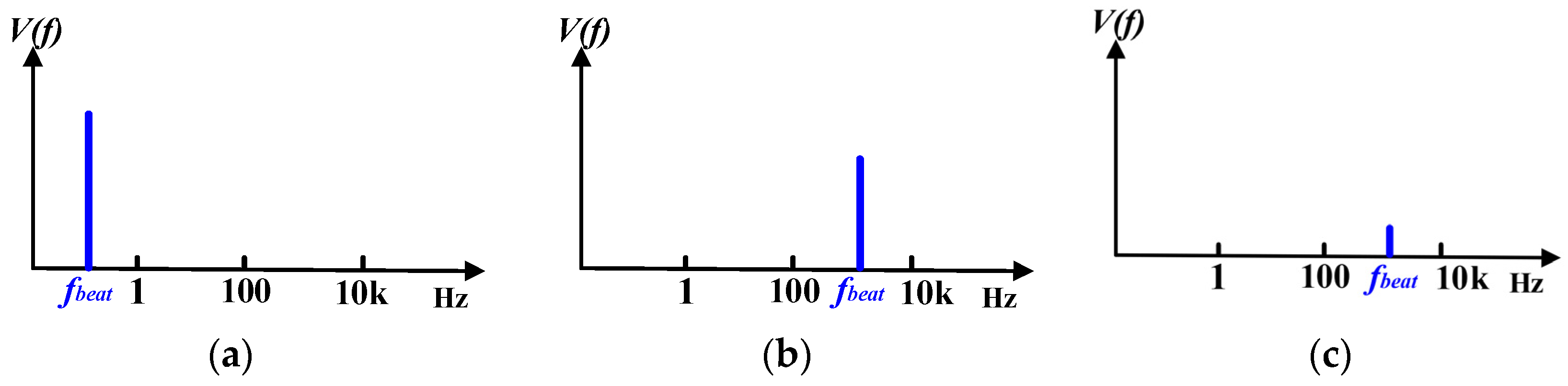
2.3. Beat Frequency Oscillation Analysis for Two Parallel-Connected Boost Converters

Based on the crossed frequency output impedance matrix model for Buck converters in [12,17], the equivalent circuit for two parallel-connected Boost converters is obtained as shown in Figure 7, where f s 1 and f s 2 are the switching frequencies of two Boost converters, Z o c l 1   and   Z o c l 2 are crossed frequency output impedances of two converters [12], Z o b e a t 1 and Z o b e a t 2 are beat frequency output impedances, Z l i n e 1 and Z l i n e 2 are line impedances, v o d c 1 and v o d c 2 are average output voltage of two converters, v o f 1 f s 1 and v o f 2 f s 2 are output switching frequency voltage ripples of two converters, and Z l o a d is the load impedance.
Assume the load impedance is much larger than the power converter output capacitor impedance at the switching frequency; the output current ripples with frequency components of f s 1 and f s 2 , which are generated by the voltage ripples v o f 1 and v o f 2 , can be expressed as:
i o 1 f s 1 = i o 2 f s 1 1 2 v o f 1 f s 1 Z o c l 1 f s 1 + Z l i n e 1 f s 1
i o 2 f s 2 = i o 1 f s 2 1 2 v o f 2 f s 2 Z o c l 2 f s 2 + Z l i n e 2 f s 2
According to Figure 6, at switching frequencies of f s 1 and f s 2 , the closed-loop impedances Z o c l 1 and Z o c l 2 are small. For DC microgrids without additional line inductors, line impedances Z l i n e 1   and Z l i n e 2 also are small. Therefore, the generated perturbation currents i o 1 f s 1 and i o 2 f s 2 will be large, and their influence on the system cannot be disregarded.
When switching frequencies f s 1 and f s 2 are close, the beat frequency impedance Z o b e a t 1 f b and Z o b e a t 2 f b for beat frequency f b = f s 1 f s 2 can be expressed as:
Z o b e a t 1 f b = v o f 2 f s 2 i o 1 f s 1 Z o c l 1 f b R d   Z o f s 2
Z o b e a t 2 f b = v o f 1 f s 1 i o 2 f s 2 Z o c l 2 f b R d   Z o f s 1
where Z o is the open-loop output impedance from Equation (5), Z o c l 1 and Z o c l 2 are the closed-loop output impedances, and R d is the droop coefficient.
Therefore, the beat frequency voltage oscillations on the output of two Boost converters can be estimated as:
v o b e a t 1 f b = Z o b e a t 1 f b i o 1 f s 2
v o b e a t 2 f b = Z o b e a t 2 f b i o 2 f s 1

3. The Proposed Hybrid Method to Mitigate the Beat Frequency Oscillation

The proposed hybrid method is based on Equations (13) and (14), and aims to reduce the beat frequency oscillations by decreasing the output current ripples ( i o 1 and i o 2 ) and beat frequency impedances ( Z o b e a t 1 and Z o b e a t 2 ) .
From Equations (9) and (10) and the review of Boost converter output voltage ripples, to reduce the output current ripples of Boost converters, a possible method is to increase the line impedances Z l i n e 1 f s 1 and Z l i n e 2 f s 2 by adding line inductors between the Boost converter output terminal and the DC bus. The selection of the line inductor values depends on the amplitude of the output voltage ripple and the requirement of the maximum beat frequency oscillation current. Based on Equation (2), if a DC microgrid with a large load current, or if the Boost converter has a high output capacitor ESR, a large line inductor is required for effective suppression of beat frequency oscillations, which will increase the cost.
From Equations (11) and (12) and Figure 4, if the difference of the switching frequency f s 1 and f s 2 (i.e., beat frequency f b ) are set to be large enough (for example, >1 kHz), the closed-loop output impedances Z o c l at the beat frequency region will be low, which means increasing the beat frequency can decrease impedances Z o b e a t 1 f b and Z o b e a t 1 f b to alleviate the perturbation. However, this method alone would require large switching frequency differences between multiple power converters, which is not feasible in some applications.
A hybrid solution is proposed, which includes both additional line inductors and switching frequency channels. From Equations (11) and (12), increasing the droop coefficient R d also can decrease the beat frequency impedances and reduce the perturbation. However, a large droop coefficient could cause a large DC bus voltage drop, so it is not considered in the proposed method.
Figure 8a shows the beat frequency components for two Boost converters with the same switching frequency setting. Due to inevitable hardware tolerance of the digital controller’s reference oscillator clock, the output voltage and currents of Boost converters have large amplitude and extra low frequency (<1 Hz) oscillations.
The proposed method introduces switching frequency channels for a DC microgrid with multiple power converters. The frequency difference between channels is determined by the number of converters in the system and other constraints. Each power converter within the DC microgrid is then assigned a specific switching frequency channel. For example, for a DC microgrid with multiple Boost converters, the switching frequencies for each converter can be set as f C H 1 , f C H 1 + Δ f C H ,…, f C H 1 + k 1 Δ f C H , respectively, where f C H 1 is the switching frequency of the first channel, Δ f C H is the frequency difference between channels, and k is the number of power converters. Consequently, the main component frequency of the beat frequency oscillations fbeat will be shifted from the extra low frequency region to the mid-frequency region of Δ f C H . In addition, because of reduced beat frequency impedance, the amplitude of the oscillation is reduced, as shown in Figure 8b.
Line inductors are then introduced between the output terminal of each Boost converter and the DC bus, which could reduce the amplitude of the switching frequency current ripple, and therefore further reduce the amplitude of the beat frequency oscillations, as shown in Figure 8c.
The main contribution of the additional line inductor is to reduce the switching frequency current perturbations, as shown in Equations (10) and (11). For Boost converters, the switching frequency voltage ripple is not a constant, and increases with the load current. Therefore, the selection of the line inductor depends on the load condition. For low nominal load current applications, a small line inductor could be selected. If the nominal load current is large, a larger line inductor is necessary. However, due to the cost of the high-current high-inductance inductors, a trade-off needs to be considered between cost and performance. Also, based on Equations (13) and (14), the beat frequency impedance is relatively large at a low frequency range, which cannot be reduced by the line inductor. Therefore, the solution of line inductors only has its limitations.
The proposed method has two main advantages: first, the setting of the switching frequency channels is flexible, making it suitable for different DC microgrid applications with multiple power converters. Second, the required inductance for the line inductor is reduced, therefore reducing the overall solution cost.
However, the proposed method also has two main limitations: first, it requires access to the control code of the power converters to change the switching frequency, which may not be possible for some commercially available power converters; second, changing the switching frequency may affect the control performance of the designed power converter controller. These limitations need to be considered when applying the proposed method in practical applications.

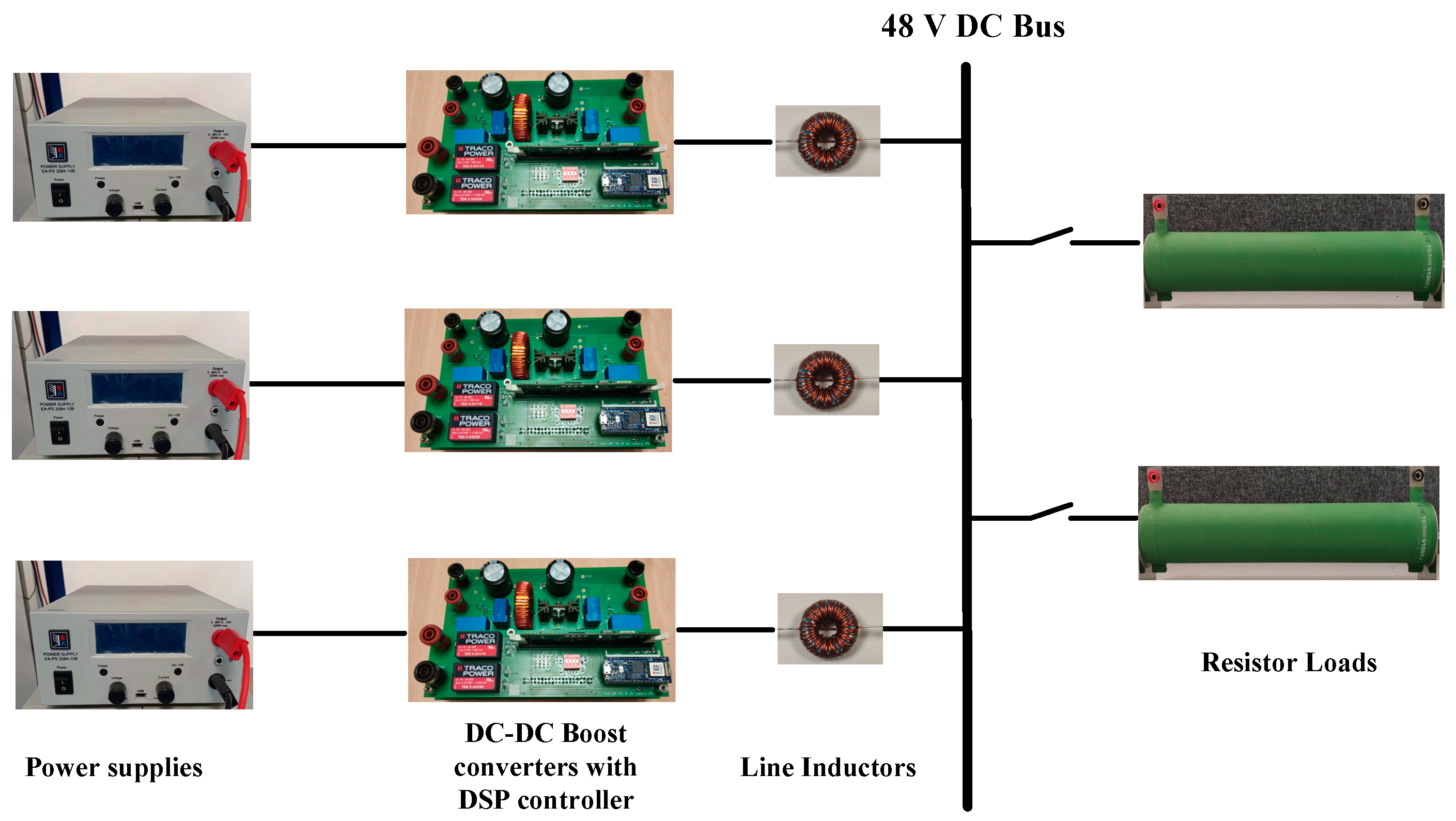
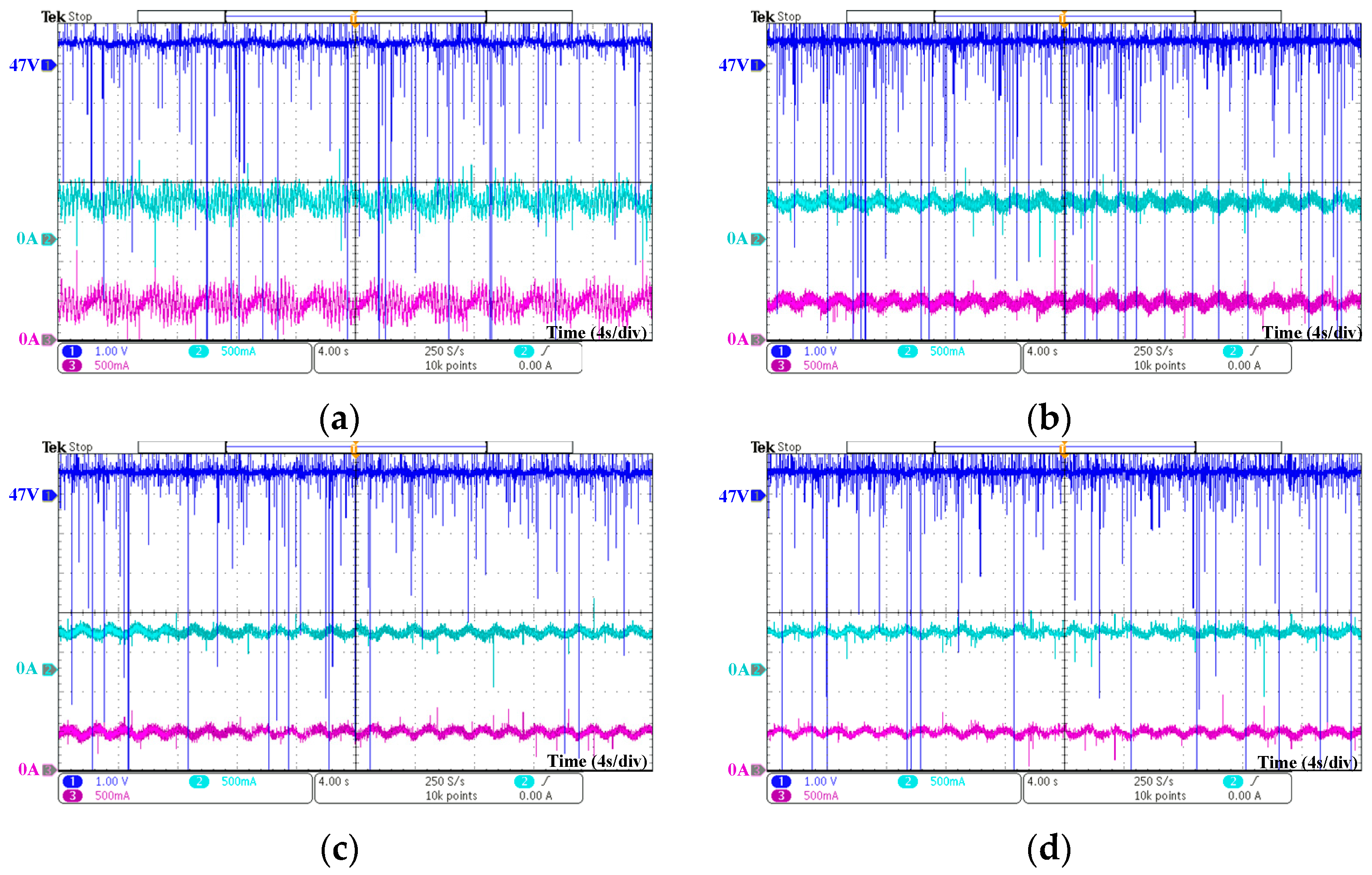
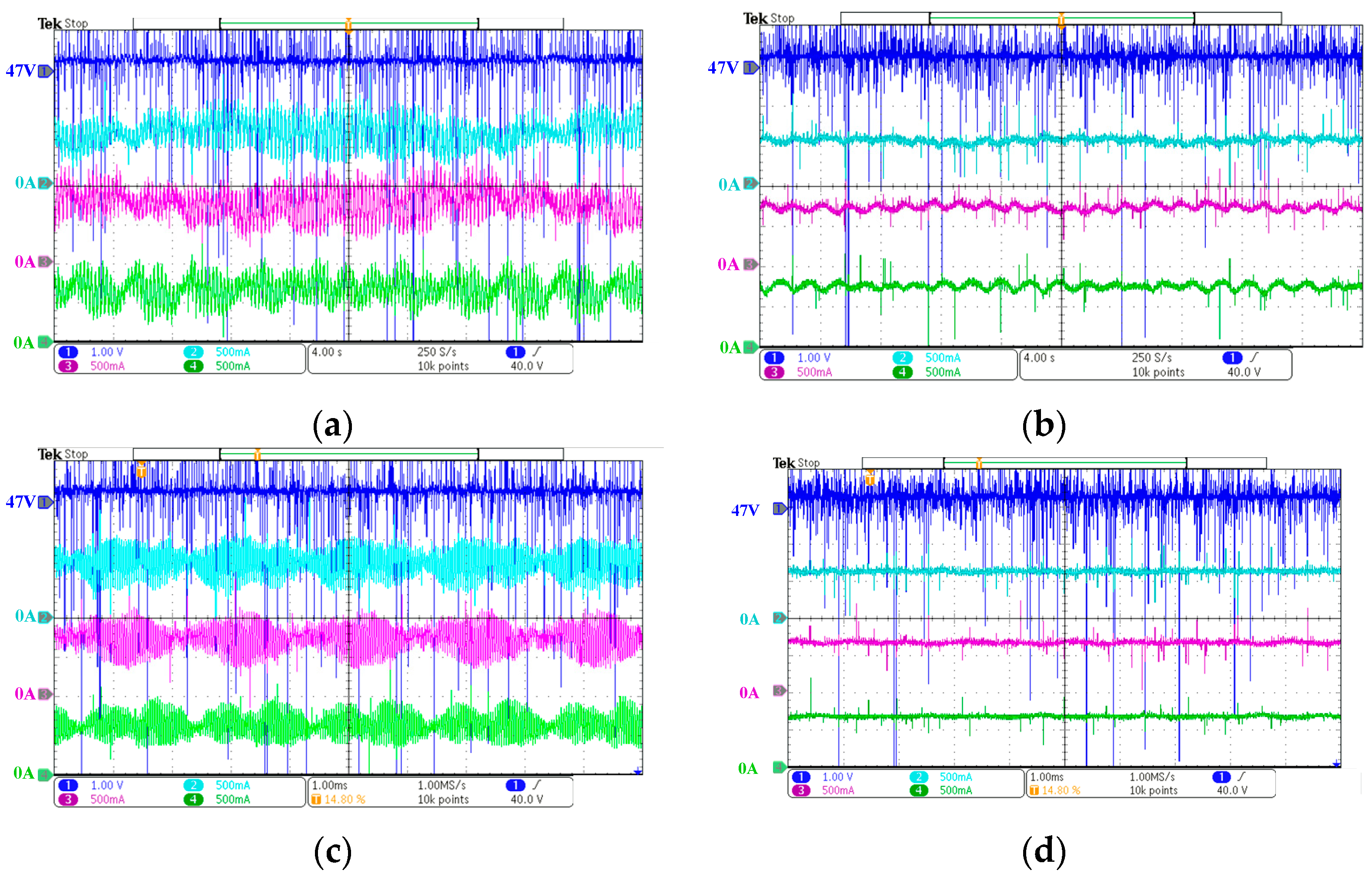
4. Experimental Verification

The proposed hybrid method has been experimentally evaluated on a DC microgrid experimental platform, as shown in Figure 9. In this experimental setup, all Boost converters are identical, and the circuit parameters are listed in Table 1. The microprocessor used for the Boost converter controller is TI’s TMS320F28335. Programmable power supplies (24 V, 160 W) are connected to the input of the Boost converters as energy sources. The nominal DC bus voltage is set as 48 V. Various inductors are connected between the Boost converters and loads to evaluate the performance of different line inductance selections. The loads consist of two 47 Ω resistor loads with switches. During the experiment, the DC bus voltage and the output current of each power converter are measured and recorded using a Tektronix MDO3024 oscilloscope (Beaverton, OR, USA). In the experimental waveforms shown in this paper, the dark blue waveform represents the DC bus voltage, while the light blue, purple, and green waveforms represent the output currents of the respective power converters.
Different switching frequency channel settings and different line inductance values are experimentally evaluated on DC microgrids with two and three parallel-connected Boost converters.

4.1. Experimental Results of a DC Microgrid with Two Parallel-Connected Boost Converters

In the first experiment, the load resistance is 47 Ω (total load current is about 1 A when the DC bus voltage is 47 V), the switching frequencies of two Boost converters are set as the same of f s 1 = f s 2 = 25 kHz. At this setting, the frequency of the beat frequency oscillation is very low. The impact of different filter inductance values (0 H, 47 µH, 220 µH, and 500 µH) on beat frequency oscillations is studied, and the experimental waveforms of converters’ output currents and DC bus voltage are shown in Figure 10.
Figure 10a shows the experimental results with a 0 H filter inductance (i.e., no filter inductor between the Boost converter output terminal and the DC bus). A very low frequency (about 0.03 Hz) oscillation can be observed, and the peak-to-peak amplitude of the current oscillation is about 0.55 A. The switching frequency difference between two Boost converters is only about 0.00012% (0.03 Hz/25 kHz), which is caused by the hardware tolerance of the different reference oscillator clocks for two micro-processors.
Figure 10b–d show the experimental results after introducing line inductors of 47 µH, 220 µH, and 500 µH, respectively. It shows that with the increase in the line inductance, the peak-to-peak amplitude of the current oscillation can be reduced. However, even with a 500 µH line inductor, the peak-to-peak amplitude of the current oscillation is still quite large, which is about 0.2 A. It shows that it is difficult to effectively mitigate this very low beat frequency oscillation only with additional line inductors.
In the second experiment, the total load current is 1 A. The switching frequencies of two Boost converters are set as f s 1 = 24.5 kHz and f s 2 = 24 kHz, respectively. Then the main component of the beat frequency oscillations will be moved to f b e a t 2 = f s 1 f s 2 = 500 Hz. Similar to the first experiment, the impact of different line inductance values is investigated, and the experimental results are shown in Figure 11.
Figure 11a shows the experimental results with a 0 H line inductance. It shows that the output currents of Boost converters have a 500 Hz beat frequency oscillation with an amplitude of about 0.4 A. Compared to the result shown in Figure 10a, it shows that increasing the beat frequency can slightly reduce the oscillation amplitude, which is as expected based on Equations (13) and (14). Figure 11b–d show the experimental results with line inductors of 47 µH, 220 µH, and 500 µH, respectively. It shows that the amplitude of the beat frequency oscillation is significantly reduced with the increase in the line inductance value.
More experiments have been conducted for different switching frequency differences (50 Hz, 1 kHz and 5 kHz). Figure 12 shows the experimental results of the 5 kHz switching frequency difference. At a total load current of 1 A, a 5 kHz beat frequency oscillation with an amplitude of 0.456 A can be observed in Figure 12a, and it is not visible when a 220 µH line inductor is added, as shown in Figure 12b.
The total load current is then increased to 2 A, and the experimental results are shown in Figure 12c,d. In Figure 12c, the 5 kHz beat frequency oscillation has an amplitude of 0.9 A. It shows that the beat frequency oscillation amplitude increases approximately in proportion to the load current, which is expected as Equation (2). The beat frequency oscillation is not visible when 220 µH line inductors are added, as shown in Figure 12d.
All the experimental data of the output currents waveforms at 1 A total load current condition are recorded, and the results are summarized in Table 2. It shows that the increase in the switching frequency difference and the line inductor inductance value can reduce the amplitude of the beat frequency oscillations. To include more power converters in the DC microgrid and reduce the cost of the line inductor, a 500 Hz difference between switching frequency channels and a 220 µH line inductor are selected as an optimal solution to mitigate the beat frequency oscillation for this experimental condition. Higher line inductance or larger frequency difference will be needed if the total load current increases.

4.2. Experimental Result of a DC Microgrid with Three Parallel-Connected Boost Converters

The effectiveness of the proposed method was experimentally investigated in a DC microgrid with three parallel-connected Boost converters. In this experiment, the total load current is 2 A.
Figure 13a shows the experimental result when all three Boost converters’ switching frequency are set as the same of f s 1 = f s 2 = f s 3 = 25 kHz, and no line inductor is connected. It shows that large low-frequency oscillations are generated in converters’ output currents. The observed beat frequency is about 0.5 Hz. It shows that the switching frequency difference between Boost converters is about 0.002% (0.5 Hz/25 kHz).
The performance of using 220 µH line inductors only is evaluated, and the experimental results are shown in Figure 13b. It shows that the beat frequency oscillations are reduced, but still visible.
The experimental result of switching frequency channels only is shown in Figure 13c. The switching frequencies of three Boost converters are set as f s 1 = 24 kHz, f s 2 = 24.5 kHz and f s 3 = 25 kHz, respectively. Both 500 Hz and 1000 Hz output current beat frequency oscillations can be observed. This 1000 Hz beat frequency is caused by switching frequencies of f s 1 = 24 kHz and f s 3 = 25 kHz. In general, for a DC microgrid with multiple switching frequency channels ( f C H 1 , f C H 1 + Δ f C H ,…, f C H 1 + k 1 Δ f C H ) , the beat frequency oscillations contain multiple frequency components ( Δ f C H ,   2 Δ f C H ,   and   k 1 Δ f C H ) , and the main component is the frequency of Δ f C H .
The experimental results of the hybrid solution (500 Hz switching frequency difference between channels and 220 µH line inductor) is shown in Figure 13d. The beat frequency oscillation is small, which verifies the effectiveness of the proposed method to mitigate the beat frequency oscillation for a DC microgrid with multiple parallel-connected Boost converters.

5. Conclusions

In DC microgrids, interactions among multiple feedback-controlled power electronic converters can cause serious beat frequency oscillation issues, which will influence the performance and power quality of DC microgrids. This paper addresses these oscillation issues in a DC microgrid with multiple parallel-connected Boost converters. Beat frequency oscillation analysis is conducted using a small-signal model. Then, a hybrid method, incorporating switching frequency channels and low pass filters, is proposed to suppress the beat frequency oscillation. The effectiveness of the proposed strategy is evaluated through experimental studies.
The proposed method requires access to the control code of the power converters, which may not be possible for some commercially available power converters. The proposed method requires additional line inductors, and the cost could be high for high-power rating applications. To address this issue, future research will be conducted on the feedback controller design, novel sampling and digital signal processing techniques, so that the size of the line inductor could be further reduced.

Author Contributions

Conceptualization, Z.L.; Methodology, H.X.; Software, H.X.; Validation, H.X.; Formal analysis, H.X.; Investigation, Z.L.; Writing—original draft, H.X.; Writing—review & editing, Z.L.; Supervision, Z.L.; Funding acquisition, Z.L. All authors have read and agreed to the published version of the manuscript.

Funding

This research was funded by UK Engineering and Physical Sciences Research Council grant number EP/S001662/2.

Data Availability Statement

The original contributions presented in the study are included in the article, further inquiries can be directed to the corresponding author.

Conflicts of Interest

The authors declare no conflict of interest.

References

  1. Xu, Q.; Vafamand, N.; Chen, L.; Dragičević, T.; Xie, L.; Blaabjerg, F. Review on Advanced Control Technologies for Bidirectional DC/DC Converters in DC Microgrids. IEEE J. Emerg. Sel. Top. Power Electron. 2021, 9, 1205–1221. [Google Scholar] [CrossRef]
  2. Guerrero, J.M.; Vasquez, J.C.; Matas, J.; De Vicuña, L.G.; Castilla, M. Hierarchical control of droop-controlled AC and DC microgrids—A general approach toward standardization. IEEE Trans. Ind. Electron. 2010, 58, 158–172. [Google Scholar] [CrossRef]
  3. Shafiee, Q.; Dragičević, T.; Vasquez, J.C.; Guerrero, J.M. Hierarchical control for multiple DC-microgrids clusters. IEEE Trans. Energy Convers. 2014, 29, 922–933. [Google Scholar] [CrossRef]
  4. Mohammadi, F.; Mohammadi-Ivatloo, B.; Gharehpetian, G.B.; Ali, M.H.; Wei, W.; Erdinç, O.; Shirkhani, M. Robust control strategies for microgrids: A review. IEEE Syst. J. 2021, 16, 2401–2412. [Google Scholar] [CrossRef]
  5. Hosseinipour, A.; Hojabri, H. Small-Signal Stability Analysis and Active Damping Control of DC Microgrids Integrated With Distributed Electric Springs. IEEE Trans. Smart Grid 2020, 11, 3737–3747. [Google Scholar] [CrossRef]
  6. Santos Neto, P.J.; dos Santos Barros, T.A.; Silveira, J.P.; Ruppert Filho, E.; Vasquez, J.C.; Guerrero, J.M. Power management strategy based on virtual inertia for DC microgrids. IEEE Trans. Power Electron. 2020, 35, 12472–12485. [Google Scholar] [CrossRef]
  7. Zhu, X.; Meng, F.; Xie, Z.; Yue, Y. An Inertia and Damping Control Method of DC–DC Converter in DC Microgrids. IEEE Trans. Energy Convers. 2020, 35, 799–807. [Google Scholar] [CrossRef]
  8. Qiu, Y.; Xu, M.; Sun, J.; Lee, F.C. A generic high-frequency model for the nonlinearities in buck converters. IEEE Trans. Power Electron. 2007, 22, 1970–1977. [Google Scholar] [CrossRef]
  9. Sun, J.; Bing, Z.; Karimi, K.J. Input impedance modeling of multipulse rectifiers by harmonic linearization. IEEE Trans. Power Electron. 2009, 24, 2812–2820. [Google Scholar] [CrossRef]
  10. Yue, X.; Wang, X.; Blaabjerg, F. Review of Small-Signal Modeling Methods Including Frequency-Coupling Dynamics of Power Converters. IEEE Trans. Power Electron. 2019, 34, 3313–3328. [Google Scholar] [CrossRef]
  11. Qiu, Y.; Xu, M.; Yao, K.; Sun, J.; Lee, F.C. Multifrequency small signal model for buck and multiphase buck converters. IEEE Trans. Power Electron. 2006, 21, 1185–1192. [Google Scholar] [CrossRef]
  12. Yue, X.; Boroyevich, D.; Lee, F.C.; Chen, F.; Burgos, R.; Zhuo, F. Beat Frequency Oscillation Analysis for Power Electronic Converters in DC Nanogrid Based on Crossed Frequency Output Impedance Matrix Model. IEEE Trans. Power Electron. 2018, 33, 3052–3064. [Google Scholar] [CrossRef]
  13. Ambatipudi, R. Simple techniques minimize cross-coupling in distributed power systems. Powerconversion Intell. Motion-Engl. Ed. 1998, 24, 8–15. [Google Scholar]
  14. Mandal, K.; Banerjee, S. Synchronization Phenomena in Microgrids With Capacitive Coupling. IEEE J. Emerg. Sel. Top. Circuits Syst. 2015, 5, 364–371. [Google Scholar] [CrossRef]
  15. Xu, H.; Zhu, Y.; Lin, Z. Beat Frequency Oscillation Analysis for a DC Microgrid with Multiple Boost Converters. In Proceedings of the 2023 IEEE 14th International Symposium on Power Electronics for Distributed Generation Systems (PEDG), Shanghai, China, 9–12 June 2023; pp. 866–870. [Google Scholar]
  16. Yue, X.; Boroyevich, D.; Burgos, R.; Zhuo, F. A frequency domain model for beat frequency oscillation analysis in microgrid. In Proceedings of the 2016 18th European Conference on Power Electronics and Applications (EPE’16 ECCE Europe), Karlsruhe, Germany, 5–9 September 2016; pp. 1–10. [Google Scholar]
  17. Yue, X.; Zhuo, F.; Yang, S.; Pei, Y.; Yi, H. A Matrix-Based Multifrequency Output Impedance Model for Beat Frequency Oscillation Analysis in Distributed Power Systems. IEEE J. Emerg. Sel. Top. Power Electron. 2016, 4, 80–92. [Google Scholar] [CrossRef]
  18. Chakraborty, S.S.; Hatua, K. Modeling with Beat Frequency Dynamics and Phase-Frequency Control Design for a Dual-Bridge Series Resonant Converter. IEEE Trans. Ind. Electron. 2022, 69, 7952–7962. [Google Scholar] [CrossRef]
  19. Yue, X.; Högrud, M. Beat Frequency Oscillation Analysis for Voltage Regulators in Telecom Power System. In Proceedings of the 2022 IEEE Applied Power Electronics Conference and Exposition (APEC), Houston, TX, USA, 20–24 March 2022; pp. 2135–2140. [Google Scholar]
  20. Ding, D.; Zhao, N.; Wang, G.; Zhang, G.; Zhang, X.; Mijatovic, N.; Xu, D. Suppression of Beat Phenomenon for Electrolytic Capacitorless Motor Drives Accounting for Sampling Delay of DC-Link Voltage. IEEE Trans. Ind. Electron. 2022, 69, 1167–1176. [Google Scholar] [CrossRef]
  21. Li, K.; Tan, S.-C.; Hui, R.S.Y. On Beat Frequency Oscillation of Two-Stage Wireless Power Receivers. IEEE Trans. Power Electron. 2020, 35, 12741–12751. [Google Scholar] [CrossRef]
  22. Alshareef, M.; Lin, Z.; Li, F.; Wang, F. A grid interface current control strategy for DC microgrids. CES Trans. Electr. Mach. Syst. 2021, 5, 249–256. [Google Scholar] [CrossRef]
Figure 1. Configuration of a typical DC microgrid.
Energies 17 03513 g001
Figure 2. Buck converter and current waveforms. (a) Buck converter circuit diagram (b) Current waveforms.
Energies 17 03513 g002
Figure 3. Boost converter and current waveforms. (a) Boost converter circuit diagram (b) Current waveforms.
Energies 17 03513 g003
Figure 4. Boost converter with a double-loop droop controller.
Energies 17 03513 g004
Figure 5. Block diagram of the small-signal model for output impedance analysis.
Energies 17 03513 g005
Figure 6. Output impedance of the boost converter.
Energies 17 03513 g006
Figure 7. Equivalent circuit for two parallel-connected Boost converters.
Energies 17 03513 g007
Figure 8. Spectrum of beat frequency oscillations. (a) Original setup. (b) With different switching frequency channels. (c) After adding line inductor.
Energies 17 03513 g008
Figure 9. Experimental setup for beat frequency oscillation investigation.
Energies 17 03513 g009
Figure 10. Experimental waveforms of Boost converter output currents and DC bus voltage with different filter inductors ( f s 1 = 25 kHz & f s 2 = 25 kHz). (a) without inductor (b) L s 1 = L s 2 = 47 µH (c) L s 1 = L s 2 = 220 µH (d) L s 1 = L s 2 = 500 µH.
Energies 17 03513 g010
Figure 11. Experimental waveforms of Boost converter output currents and DC bus voltage with different filter inductors. ( f s 1 = 24.5 kHz & f s 2 = 25 kHz). (a) without inductor (b) L s 1 = L s 2 = 47 µH (c) L s 1 = L s 2 = 220 µH (d) L s 1 = L s 2 = 500 µH.
Energies 17 03513 g011
Figure 12. Experimental waveforms of Boost converter output currents and DC bus voltage with different filter inductors ( f s 1 = 25 kHz & f s 2 = 30 kHz). (a) 1 A load current, without inductor (b) 1 A load current, L s 1 = L s 2 = 220 µH. (c) 2 A load current, without inductor (d) 2 A load current, L s 1 = L s 2 = 220 µH.
Energies 17 03513 g012
Figure 13. Experimental waveforms of Boost Converter output currents and DC bus voltage. (a) f s 1 = 25 kHz & f s 2 = 25 kHz & f s 3 = 25 kHz without inductors. (b) f s 1 = 25 kHz & f s 2 = 25 kHz & f s 3 = 25 kHz with 220 µH line inductors. (c) f s 1 = 24 kHz & f s 2 = 24.5 kHz & f s 3 = 25 kHz without inductor. (d) f s 1 = 24 kHz & f s 2 = 24.5 kHz & f s 3 = 25 kHz with 220 µH line inductors.
Energies 17 03513 g013
Table 1. Circuit parameters of the Boost converter under droop control.
ParametersValue
Switching frequency fs25 kHz
Input voltage Vin25 V
Output voltage Vo50 V
Inductor L500 µH
Capacitor C470 µF
ESR of inductor RL37 mΩ
ESR of capacitor Rc8 mΩ
Load resistor R47 Ω
Voltage loop PI compensator Kvp,Kvi0.90, 175.9
Current loop PI compensator Kip,Kii0.02, 30.3
Droop coefficient Rd1 Ω
Table 2. Beat frequency oscillations peak-to-peak amplitude for output current of Boost converters at 1 A total load current condition.
Filter Inductance0 µH47 µH220 µH500 µH
Oscillation Amplitude (A)
Switching Frequency Channels
fs1 = 25.0 kHz, fs2 = 25.0 kHz0.5540.2410.2200.204
fs1 = 24.95 kHz, fs2 = 25.0 kHz0.5480.1940.1280.104
fs1 = 24.5 kHz, fs2 = 25.0 kHz0.4920.1630.0850.063
fs1 = 24.0 kHz, fs2 = 25.0 kHz0.4800.1620.0760.052
fs1 = 25.0 kHz, fs2 = 30.0 kHz0.4560.1620.0550.051
Disclaimer/Publisher’s Note: The statements, opinions and data contained in all publications are solely those of the individual author(s) and contributor(s) and not of MDPI and/or the editor(s). MDPI and/or the editor(s) disclaim responsibility for any injury to people or property resulting from any ideas, methods, instructions or products referred to in the content.

