Article

Dead-Time Free Modulation Scheme for IM Drive System Fed by Voltage Source Inverter

State Key Laboratory of Power Transmission Equipment Technology, School of Electrical Engineering, Chongqing University, Chongqing 400044, China
*
Author to whom correspondence should be addressed.
Energies 2024, 17(15), 3845; https://doi.org/10.3390/en17153845
Submission received: 10 July 2024 / Revised: 27 July 2024 / Accepted: 30 July 2024 / Published: 5 August 2024

Abstract

:
During the modulation process of the VSI motor drive system, the nonlinear errors caused by the dead-time and conduction voltage drop will increase the phase current harmonic distortion and the torque ripple. To solve this problem, a novel dead-time free modulation scheme is proposed in this paper. In the non-zero crossing region of the phase current, the switching tube, whose body diode can provide a continuation path, is set as off-state, the driving signal is only implemented on another switching tube with the same bridge arm, and the errors caused by the conduction voltage drop and switching delay are compensated to the pulse duration. At the same time, to suppress the zero current clamp effect that exists near the zero crossing point of the phase current, another modulation scheme for the phase current crossing zero in advance is proposed, which avoids the complicated determination and calculation of the current polarity near the zero crossing point of the current. Both of the above modulation schemes eliminate the dead-time, and the switching principle is presented. In addition, to suppress the impact of the current ripple and high-frequency noise on the accuracy of the phase current detection, a second-order resonance digital filter without phase shift is introduced. Finally, compared to two deadtime compensation methods, the effectiveness and superiority of the proposed dead-time free modulation scheme are verified by the experimental results.

1. Introduction

Developing electric vehicles can slow down the pace of global climate change [1], reduce pollution, and effectively save energy [2]. Among numerous inverter topologies, the voltage source inverter (VSI) has fewer power devices, a simple structure, and mature and easy control technology, so it is the most commonly used drive topology in electric vehicles [3]. To prevent short-circuits occurring in the VSI bridge arm, the turn-on process of all switching tubes requires a delay, so the dead-time is formed, and both switching tubes of the upper and lower bridge arms are in the off-state [4]. The dead-time and conduction voltage drop lead to a nonlinear error in the VSI output voltage; especially for electric vehicle drive systems, the stator current harmonic distortion and torque ripple caused by the nonlinear voltage error cannot be ignored [5], because the electric vehicles will experience noticeable bumps and whistles [6]. For sensorless systems, the output voltage nonlinear error will reduce the accuracy of the flux and speed observers [7].
To solve the above problem, multiple nonlinear voltage compensation or suppression strategies have been proposed. Pulse time compensation is the most traditional and commonly used method for suppressing the nonlinear error, which converts the voltage error caused by the dead-time and conduction voltage drop based on the stator current polarity into a PWM pulse width within one switching period and compensates for it [8]. Reference [9] considers the influence of the snubber and parasitic capacitance in the pulse compensation, further improving the compensation accuracy. In [10], the average nonlinear error of the three-phase voltage for each switching cycle is converted to the stationary coordinate system, then the voltage error is compensated in the voltage reference. Reference [11] considers the nonlinear voltage error of the inverter as the disturbance and decomposes it into voltage errors caused by dead-time under the snubber capacitance and voltage errors caused by the conduction voltage drop. Meanwhile, the corresponding feedforward compensation calculation methods are proposed for two types of voltage errors. An improved trapezoidal voltage compensation method is proposed in [12]; except for the trapezoidal angle, the amplitude of the trapezoidal voltage is also controlled, which can significantly improve the compensation performance. However, the above methods all belong to the offline compensation and can only correct the fundamental amplitude, but the harmonic suppression effect is not obvious. Reference [13] analyzes the harmonics caused by the dead-time and conduction voltage drop, it mainly contains fifth and seventh components, so the fifth and seventh harmonics of the phase current are mapped into the DC component, and then four PI controllers are adopted to obtain the compensation in the d-q coordinate system, but the compensation algorithm is too complex, and multiple PI parameters are needed to be tuned. After the Park transformation, the harmonics are mapped to sixth order in the d-q coordinate system, and then a parallel connection control structure between the proportional resonance (PR) controller and the current PI controller is proposed in [14]. Although the PR controller can suppress the fifth and seventh harmonics in the phase current, the dynamic response of the vector control system is affected. References [15,16] regard the voltage error caused by the dead-time as a voltage disturbance and use a disturbance observer to compensate for the dead-time. A compensation strategy based on an extended state observer (ESO) is proposed in [15]. To solve the frequency adaptation issue, a discrete multifrequency disturbance observer is proposed in [16]. A dead-time control scheme for bidirectional inductive power transfer converters is proposed in [17]. To minimize the loss and guarantee the zero-voltage switching of MOSFETs, the turn-on delay, turn-off delay, and the discharge time offline are measured and stored in the microcontroller. Then, using a lookup table, the optimal minimum deadtime is obtained based on the turn-off current and DC voltage levels, and the dynamic optimal minimum deadtime control scheme can be realized. However, this method is only suitable for applications of zero-voltage switching, and offline measurement of MOSFET switching characteristics can also be cumbersome.
The above method cannot completely eliminate the influence of the dead-time, especially at high speeds, because the frequency of the voltage disturbance caused by the dead- time is very high and difficult to observe. In this paper, a novel dead-time-free modulation scheme is proposed; according to the analysis of the phase current flow path under different polarities, the switching tube, whose body diode can provide a continuation path, can be set as off-state, so the driving signal is only implemented on another switching tube with the same bridge arm. Since there is only one switching tube in the action state in one leg, the dead-time is not needed. However, due to the zero current clamp effect, the proposed modulation scheme cannot be applied near the zero crossing point of phase current [18], and the switching state remains the maximum voltage output that can make the current cross zero point in advance. Meanwhile, since the proposed dead-time free modulation requires extremely high accuracy in phase current detection, a high-precision digital filter is designed to eliminate the influence of the high-frequency ripple and sampling noise. This paper is organized as follows:
The nonlinear voltage error caused by the dead-time and conduction voltage drop, and the zero current clamp effect near the zero crossing point of the phase current are analyzed in Section 2. The dead-time free modulation strategy in the non-zero crossing region is proposed in Section 3, and the modulation scheme for the phase current crossing zero in advance is proposed in Section 4. On this basis, the principle for switching the two proposed modulation schemes is presented in Section 5. To improve the accuracy of the phase current detection, a second-order bandpass digital filter without phase shift is presented in Section 6. Finally, the performance of the proposed dead-time free modulation strategy for VSI is verified by the experimental results in Section 7 and compared with other dead-time compensation methods.

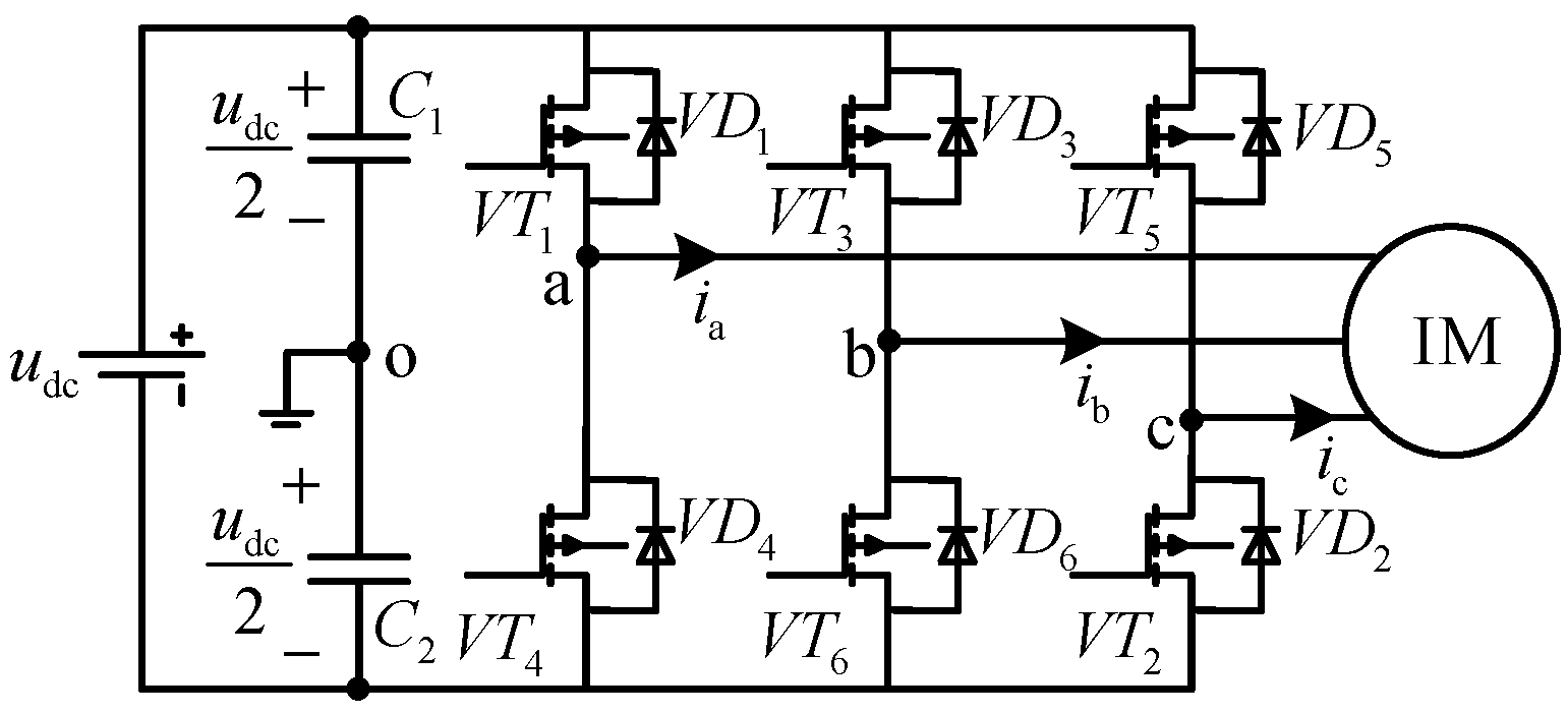
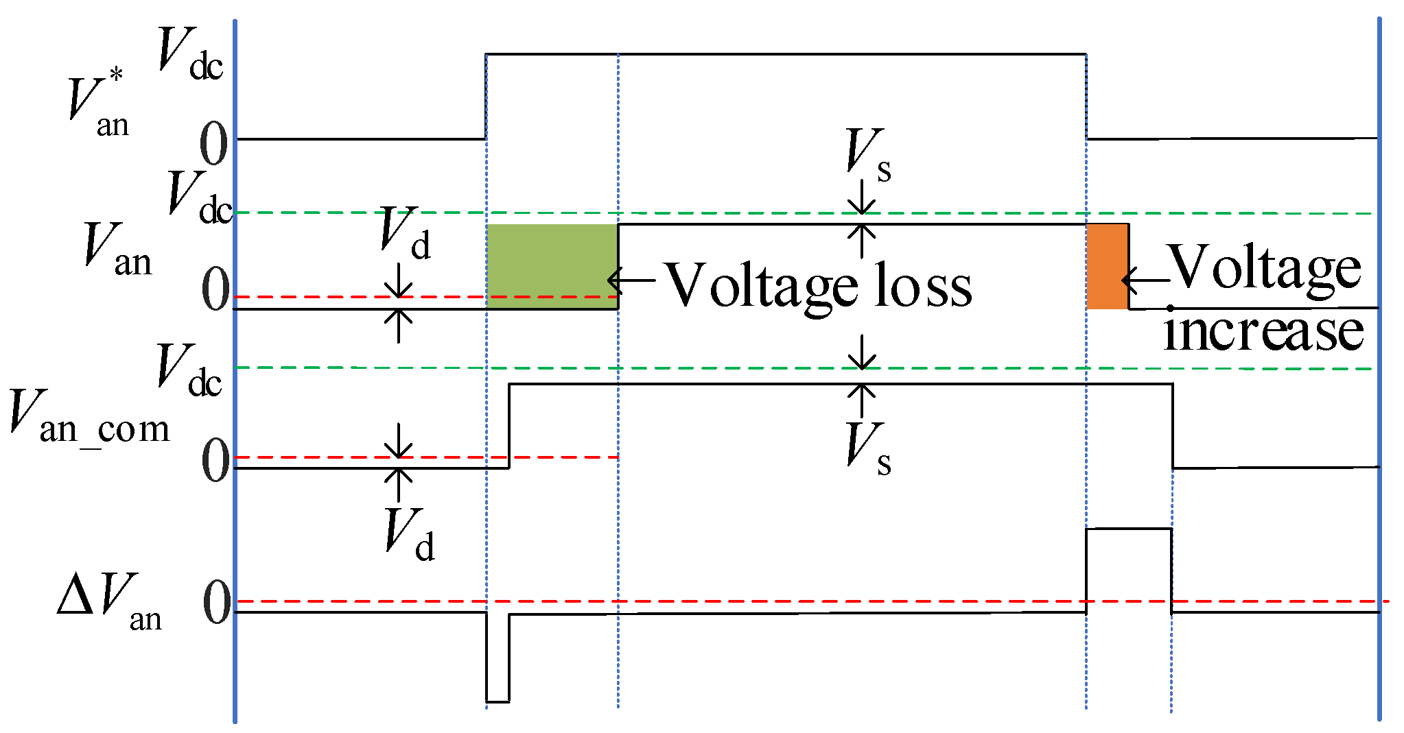
2. Nonlinear Voltage Error Analysis of VSI

This paper takes the induction motor (IM) drive system fed by VSI as the research object; the topology is shown in Figure 1. Next, taking a phase-A bridge arm as an example, the nonlinear voltage error caused by the dead-time and conduction voltage drop and the zero current clamp effect near the zero crossing point of phase current are analyzed, respectively.

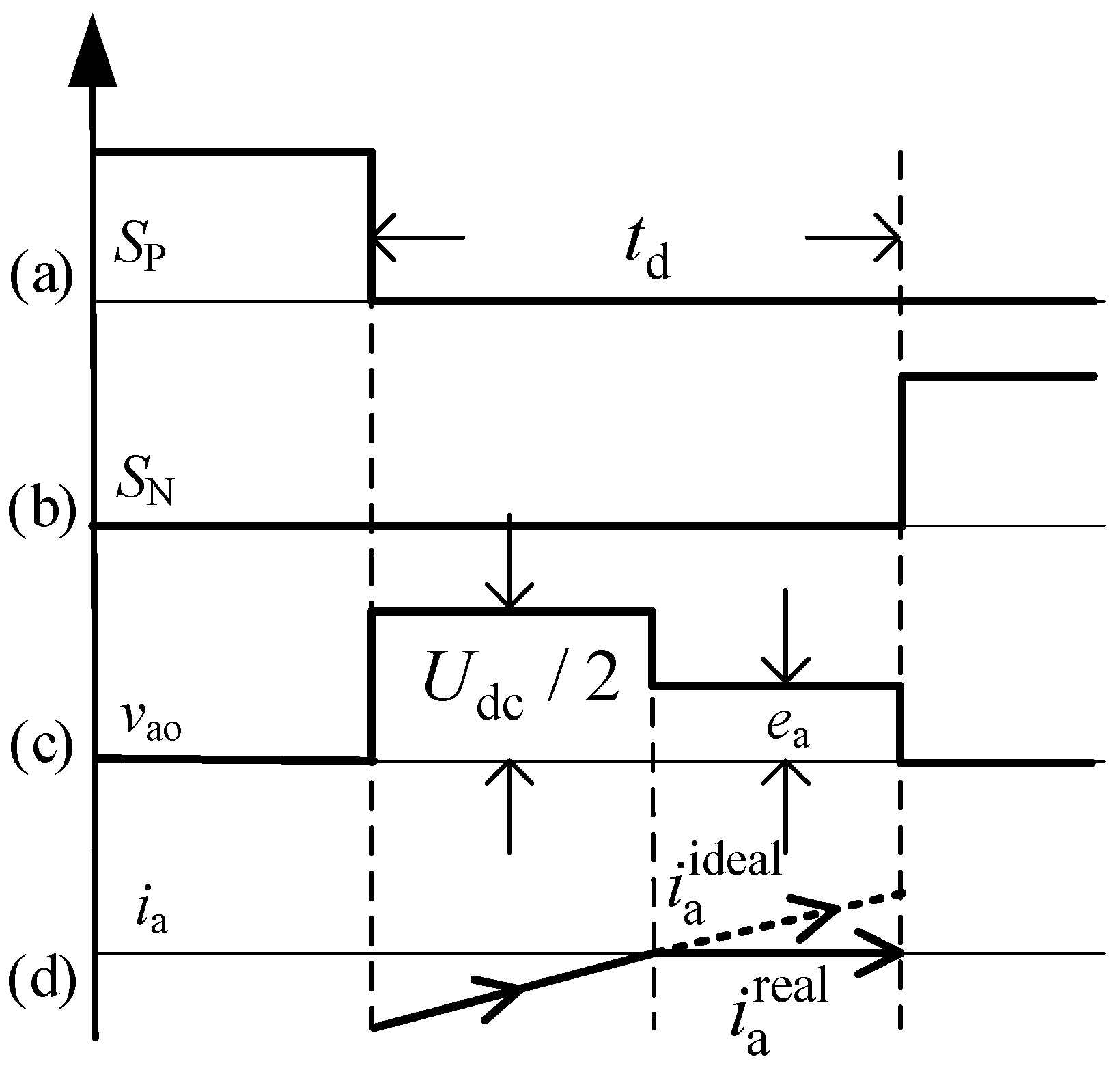
2.1. Nonlinear Voltage Error Caused by the Dead-Time and Conduction Voltage Drop

The schematic diagram of phase-A in VSI is shown in Figure 2. When the phase current ia > 0, if the upper phase leg switching tube VTP is turned on, the current flows through VTP; otherwise, when the upper phase leg switching tube is turned off and the lower phase leg switching tube is turned on, the current will not flow through VTN, but will continue to flow through the diode VDN. It means that when the phase current ia > 0, no matter whether the VTN is turned on or off, it will not work. Similarly, when the phase current ia < 0, VTP is in an invalid state.
Since the switching tube has an inherent turn-off delay, to prevent the upper phase leg and the lower phase leg from being turned on at the same time and causing a short circuit, the switching tube needs to be turned on with a delay, that is, a dead-time is inserted. During the dead-time, the upper and lower phase legs are not turned on, and the current is only continued through the parallel diode VDP and VDN. In addition, the tube conduction voltage drop and switching delay also increase the voltage error of the inverter.
The dead-time effect of a single phase leg in VSI is shown in Figure 3, where PWMH* and PWML* are ideal complementary drive signals; PWMH and PWML are the actual drive signals applied to the switching tubes after adding the dead-time; SP and SN are the actual switch waveforms considering the turn-on and turn-off delays; td is the dead-time; ton is the turn-on delay time; toff is the turn-off delay time; Vd is the diode conduction voltage drop; Vs is the switch tube conduction voltage drop.
As shown in Figure 3, the sources of nonlinear voltage error are divided into three aspects: the addition of dead-time, the switching delay of the switching tube, and the conduction voltage drop. The voltage error analysis of the specific switching process is as follows:
(1)
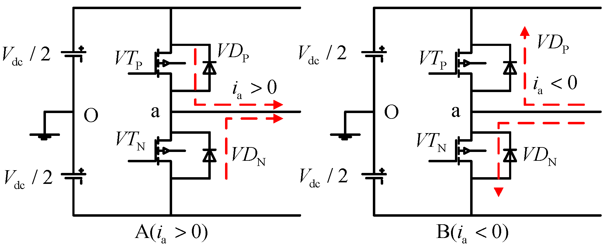
When the phase-A current satisfies ia > 0.
Taking into account the dead time and the switching delay of the switch tube, the actual VTP on-time in one period is t5t3 = DTs + tofftdton, and the VTP on-time is reduced by τ = DTs − (t5t3) = td + tontoff, where D is the duty cycle, and Ts is the PWM period. Considering the conduction voltage drop of the power electronic device, when VTP is turned on, the output voltage vao is Vdc/2 − Vs; when VTP is turned off, the current flows through VDN, and the output voltage vao = − Vdc/2 − Vd.
(2)
When the phase-A current satisfies ia < 0.
Assuming that the upper phase leg conduction time is DTs in the ideal case, the lower phase leg turn-off time is also DTs. The actual VTN off-time in one period is t7t1 = DTs + + td + tontoff, and the on-time is (1 − D) Tsτ; the on-time is reduced by τ = td + tontoff. Considering the tube voltage drop, when VTN is turned on, the output voltage vao is –Vdc/2 + Vs; when VTN is turned off, the current flows through VDP, and the output voltage vao = Vdc/2 + Vd.
It can be concluded that the reduction in VTN on-time and the conduction voltage drop of the device both cause an increase in voltage, so the on-time needs to be compensated.
According to the voltage–time area equivalence principle, Verror, the average voltage error (the difference between the ideal output voltage and the actual output voltage) caused by the above factors in one PWM period can be expressed as follows:
{ V error = τ V dc + ( D T s τ ) V s + [ ( 1 D ) T s + τ ] V d T s ( i a > 0 ) V error = τ V dc + ( D T d + τ ) V d + [ ( 1 D ) T s τ ] V s T s   ( i a < 0 ) .
According to Equation (1), the three factors of the inverter nonlinear voltage error are the addition of dead time, the conduction voltage drop, and the switching delay of the switching tube. The dead-time is the main source of voltage error.

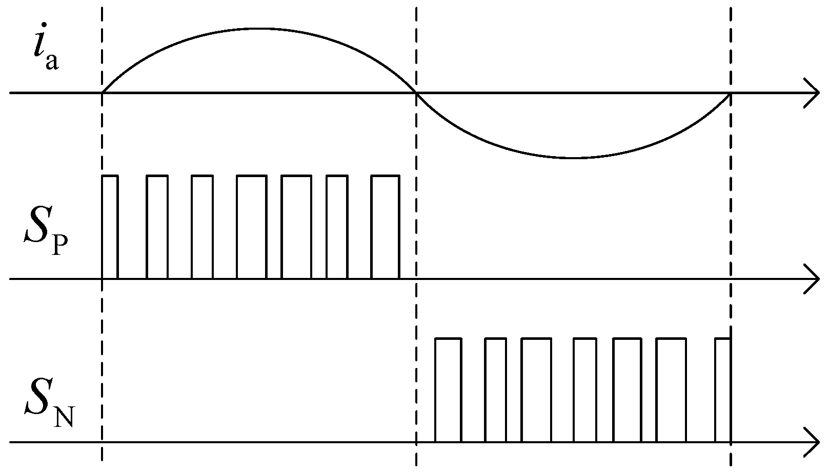
2.2. Zero Current Clamping Effect When the Phase Current Crosses Zero

The zero current clamping phenomenon is mainly caused by the dead-time. The phase current crosses the zero point during the dead-time; both the upper and lower phase legs are turned off at this time. Due to the interaction between the back electromotive force and the DC bus voltage, the diode that should continue to flow after zero crossing cannot be turned on. As a result, the current is clamped at the zero and cannot smoothly cross zero during the entire dead-time until the next switching signal arrives. If the driving voltage provided by the controller is insufficient, the current may remain near zero for multiple PWM periods, and a current “stage” will appear. Shown in Figure 4a,b are the upper and lower phase leg driving signals, (c) is the actual voltage vao between point a and point o, the dotted line in (d) is the ideal current i a ideal after crossing the zero point, and the solid line is the actual current i a real .

3. Dead-Time Elimination Strategy near Non-Zero Crossing Points

Regardless of whether the phase current ia is positive or not, there will always be a switching tube in an invalid state of one phase leg. Therefore, in the PWM period where the phase current does not cross zero, only one switching tube is activated in one phase leg. The principles are as follows:
{ S P = P W M H     S N = 0   ( i a > 0 ) S N = P W M L     S P = 0   ( i a < 0 ) .
When the phase current satisfies ia > 0, VTN is turned off; when the phase current satisfies ia < 0, VTP is turned off. Since there is a switching tube that is turned off in each PWM period, there is no need to consider the short circuit of the phase leg, and there is no need to add the dead-time. Figure 5 is the schematic diagram of ideal dead-time elimination without considering the zero crossing point.
At this time, only the nonlinear voltage error caused by the conduction voltage drop and the switching delay on the inverter need to be considered, it can be compensated by adjusting the pulse duration, the compensation time is derived by (1):
{ t com + = λ V dc + ( D T s λ ) V s + [ ( 1 D ) T s + λ ] V d ( V dc + V d V s ) t com = λ V dc + ( D T s + λ ) V d + [ ( 1 D ) T s λ ] V s ( V dc + V d V s )
where λ = tontoff, tcom+ is the increased on-time of the upper phase leg when ia > 0, and tcom− is the increased on-time of the lower phase leg when ia < 0. According to the polarity of the current, the on-time of the phase-A is determined as follows:
{ t ahon = t ahon + t com +   ( i a > 0 ) t alon = t alon + t com ( i a < 0 )
where tahon represents the turn-on time of the upper phase leg before compensation; t*ahon represents the turn-on time after compensation. At the same time, the lower phase leg remains off-state; talon represents the turn-on time of the lower phase leg before compensation; t*alon represents the turn-on time after compensation. At the same time, the upper phase leg remains off-state.

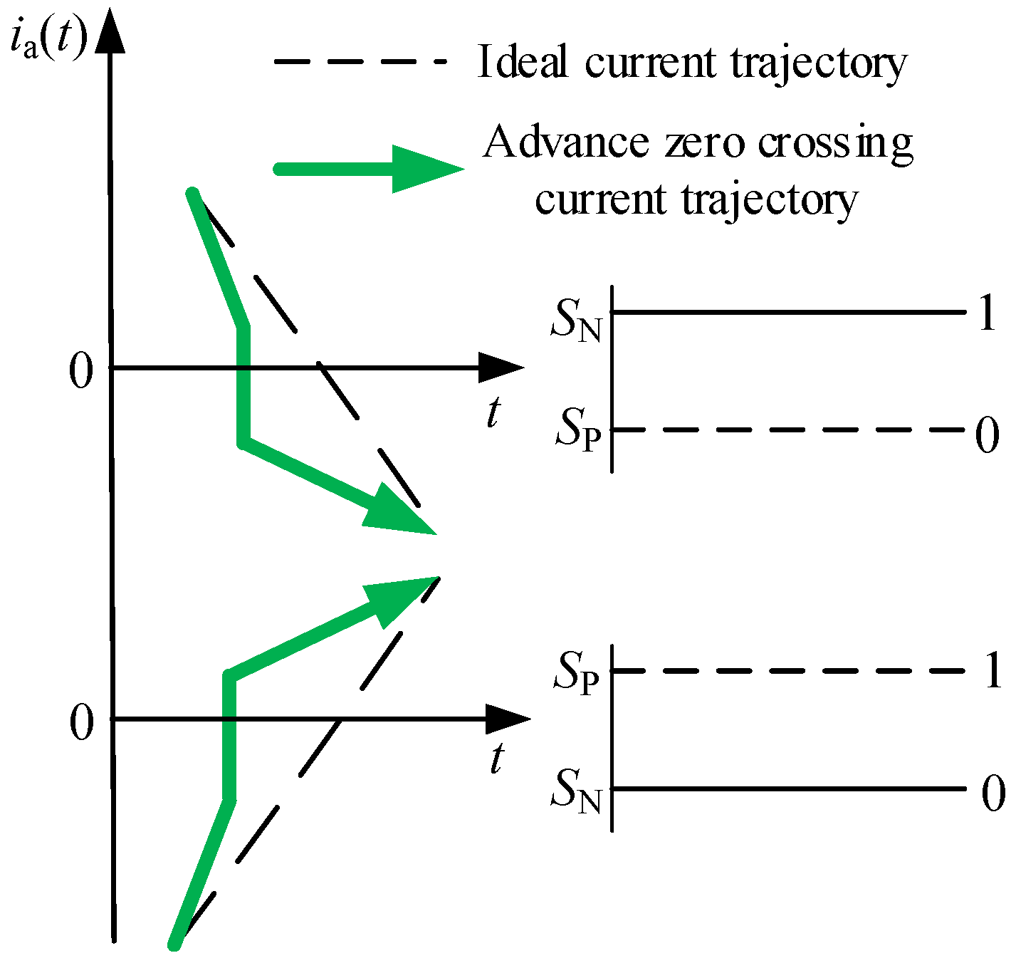
4. Modulation for the Phase Current Crossing Zero in Advance

According to the analysis in Section 2.2, the zero current clamping effect occurs when the phase current crosses zero, and it is difficult to be suppressed through voltage compensation. Therefore, a novel modulation scheme for the phase current crossing zero in advance is proposed in this paper; the diagram is shown in Figure 6. When ia crosses zero from positive to negative, to accelerate the zero crossing process of ia, the upper switching signal SP remains off-state, and the lower switching signal SN remains on-state. When ia crosses zero from negative to positive, the upper switching signal SP remains on-state, and the lower switching signal SN remains off-state. Due to generating the maximum voltage, whose polarity is the same as the changing direction of ia, the zero current clamping effect only occurs during a very short time, and it has little impact on the phase current. In addition, the dead-time is also eliminated when ia crosses zero, because no action occurs in the switching signals.

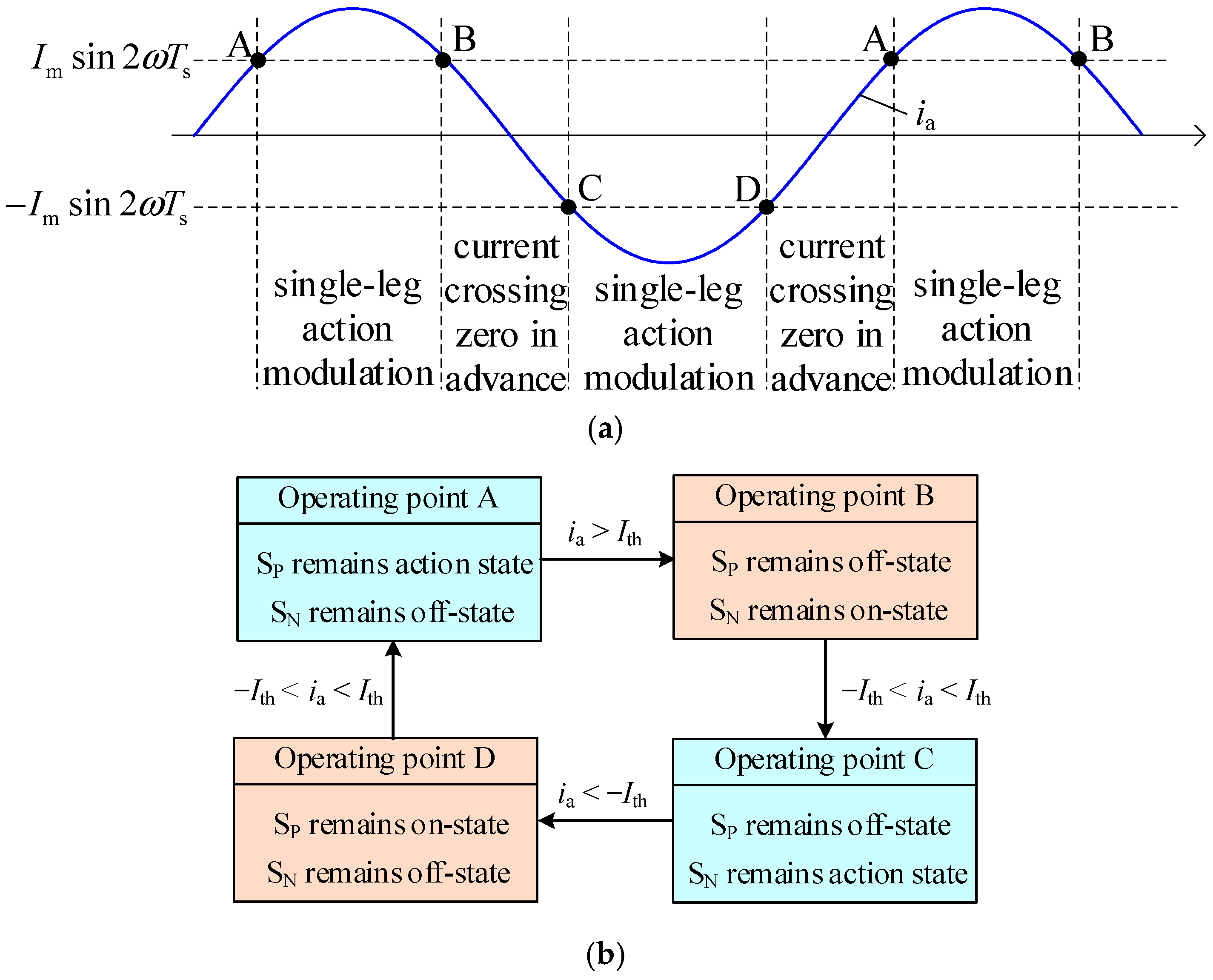
5. Selection Principle of the Two Proposed Modulation Schemes

The proposed modulation strategy for the phase current crossing zero in advance is only suitable for near the zero crossing point; in the non-zero crossing region of phase current, the proposed single-leg action modulation scheme should be applied as much as possible. Otherwise, it will cause serious harmonic distortion in the phase current. Therefore, to adopt the optimal modulation scheme for all operating points, it is necessary to determine the principle of switching the proposed two modulation schemes.
In this paper, the phase current and motor speed are sampled in real time. The three-phase stator current is subjected to Clarke transformation and rotor flux orientation-based Park transformation to obtain the stator d-q axis current isd and isq in the two-phase rotating coordinate system. Then, the real-time electrical angular frequency ωn and the phase current amplitude Im are calculated. The calculation expression is as follows:
ω n = ω f + p ω r = i sd T r i sq + p ω r
I m = i sd 2 + i sq 2
where ωf is the motor slip frequency, Tr is the rotor time constant, ωr is the actual rotor speed, and p represents the number of IM pole pairs.
During the experiment, the A/D sampling is triggered by the PWM signal. After the A/D conversion is completed, the interrupt service program is entered to update the modulation strategy and comparison value register of the next period. Therefore, there is a time interval of less than Ts between the A/D sampling time and the start time of the next PWM period. The zero crossing moment may be located at any position in this PWM period. The maximum time interval between the A/D sampling moment of the PWM period modulation strategy (i.e., the A/D sampling moment in the previous PWM period) and the zero crossing moment in this PWM period is determined to be 2 Ts, and the absolute value of the phase current at this time is |Imsin2ωnTs|. Therefore, Imsin2ωnTs and −Imsin2ωnTs are used as two threshold values and compared with the real-time sampling value of the phase current, determining the modulation scheme to be applied for the next PWM period. The diagram for the switching principle of the two modulation schemes is shown in Figure 7a; four operating points (A, B, C, and D) are defined for comparison with ia and shown as follows:
{ Point   A : i a = I th   and   i a   is   increasing Point   B : i a = I th   and   i a   is   decreasing Point   C : i a = I th   and   i a   is   decreasing Point   D : i a = I th   and   i a   is   increasing
where Ith is equal to Imsin2ωnTs. When the IM operates at point A, the proposed single-leg action modulation is applied, and the switching action only occurs in SP; SN remains off-state. Until the IM operating at point B, the proposed modulation strategy for the phase current crossing zero in advance is applied, SP and SN remain on-state and off-state, respectively. Due to the continuous output of the maximum negative polarity voltage, ia can quickly cross zero point. When the IM operates at point C, the proposed single-leg action modulation is applied again, and the switching action only occurs in SN; SP remains off-state. Until the IM operating at point D, the proposed modulation strategy for the phase current crossing zero in advance is applied again; SP and SN remain off-state and on-state, respectively. Due to the continuous output of the maximum positive polarity voltage, ia can quickly cross the zero point. The state transition diagram of the above process is shown in Figure 7b.

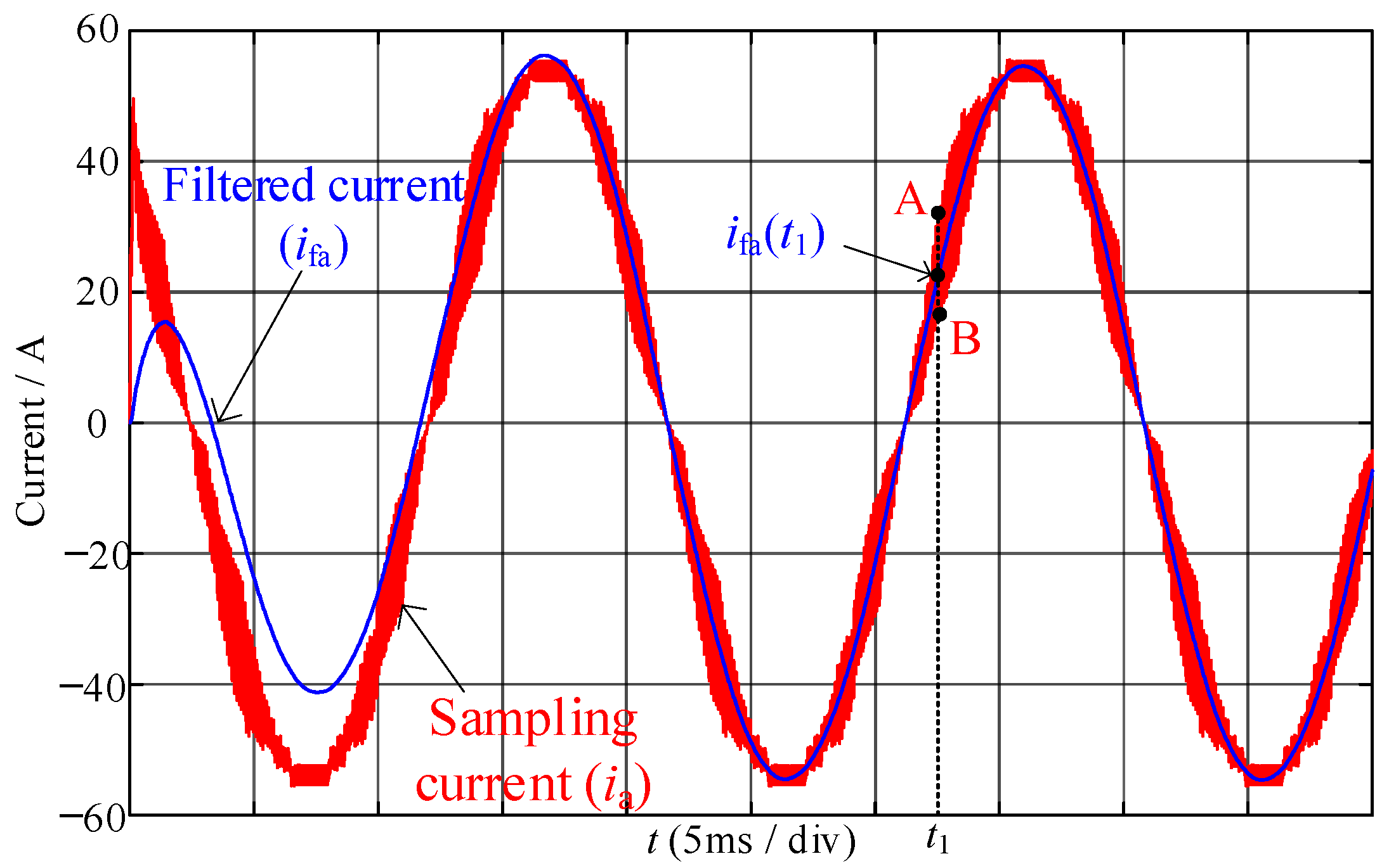
6. Discrete Filtering Processing of the Sampling Current

The switching algorithm proposed in Section 5 has extremely high requirements for current sampling accuracy. However, affected by the current ripple and sampling burrs, There may be errors between the current sampling value and the actual value, which leads to incorrect modulation strategy being adopted. A second-order resonance filter F(s) without phase shift is adopted to obtain the fundamentals of phase current. The transfer function F(s) in s-domain is expressed as follows:
F ( s ) = i fa ( s ) i ( s ) = 2 ξ ω n s s 2 + 2 ξ ω n s + ω n 2 .
where ξ is the damping ratio; ω n is the resonance frequency of the filter. ω n should be equal to the electrical angular frequency of the IM. When ξ is larger, the response speed is faster, but the high-frequency component attenuation is smaller, so the value of ξ should be chosen reasonably. After multiple simulations and comparisons, ξ is set as 0.05 in this paper. The Bode plot of F(s) under ω n = 100π rad/s is shown in Figure 8. The amplitude and phase of F(s) are 0 dB and 0 deg at 100π rad/s, and it has an attenuation effect on all other harmonic components.
Since DSP is only used to implement the discrete algorithm, discretization of Equation (8) is required. Firstly, the state equation of (8) is derived as follows:
d 2 i fa ( t ) d t 2 + 2 ξ ω n d i fa ( t ) d t + ω n 2 i fa ( t ) = 2 ξ ω n d i a ( t ) d t
The discretization using the forward difference method yields the differential expression of the digital filter as follows:
i fa [ ( n + 2 ) T s ] = 2 ( 1 ξ ω n T s ) i fa [ ( n + 1 ) T s ] ( 1 2 ξ ω n T s + ω n 2 T s 2 ) i fa ( n T s ) + 2 ξ ω n T s i a [ ( n + 1 ) T s ] 2 ξ ω n i a ( n T s )
After digital filter processing, ifa is compared with Ith to determine the modulation scheme. Since the electrical angular frequency of the IM is not a fixed value, ωn is be updated in real-time at each PWM period. The waveforms of the phase current before and after the digital filter are shown in Figure 9. ia is the sampling current, with the current ripple and sampling burrs. When the second-order bandpass digital filter is adopted, after one period, the filter current ifa can follow the fundamental component of ia without phase shift. Therefore, in the steady state, the designed digital filter can obtain the fundamental component of the phase current.
Next, the necessity of extracting the fundamental will be explained, combined in Figure 9. At t1 moment, affected by the current ripple and sampling burrs, the sample value of the phase current may be ia(A) or ia(B), and there is significant error between them. However, incorrect sampling values may result in inappropriate modulation algorithms being used in the next switching period, so this paper adopts the fundamental component obtained by the proposed digital filter as the basis for selecting the modulation. The flow chart of the modulation selection based on the digital filter is shown in Figure 10.

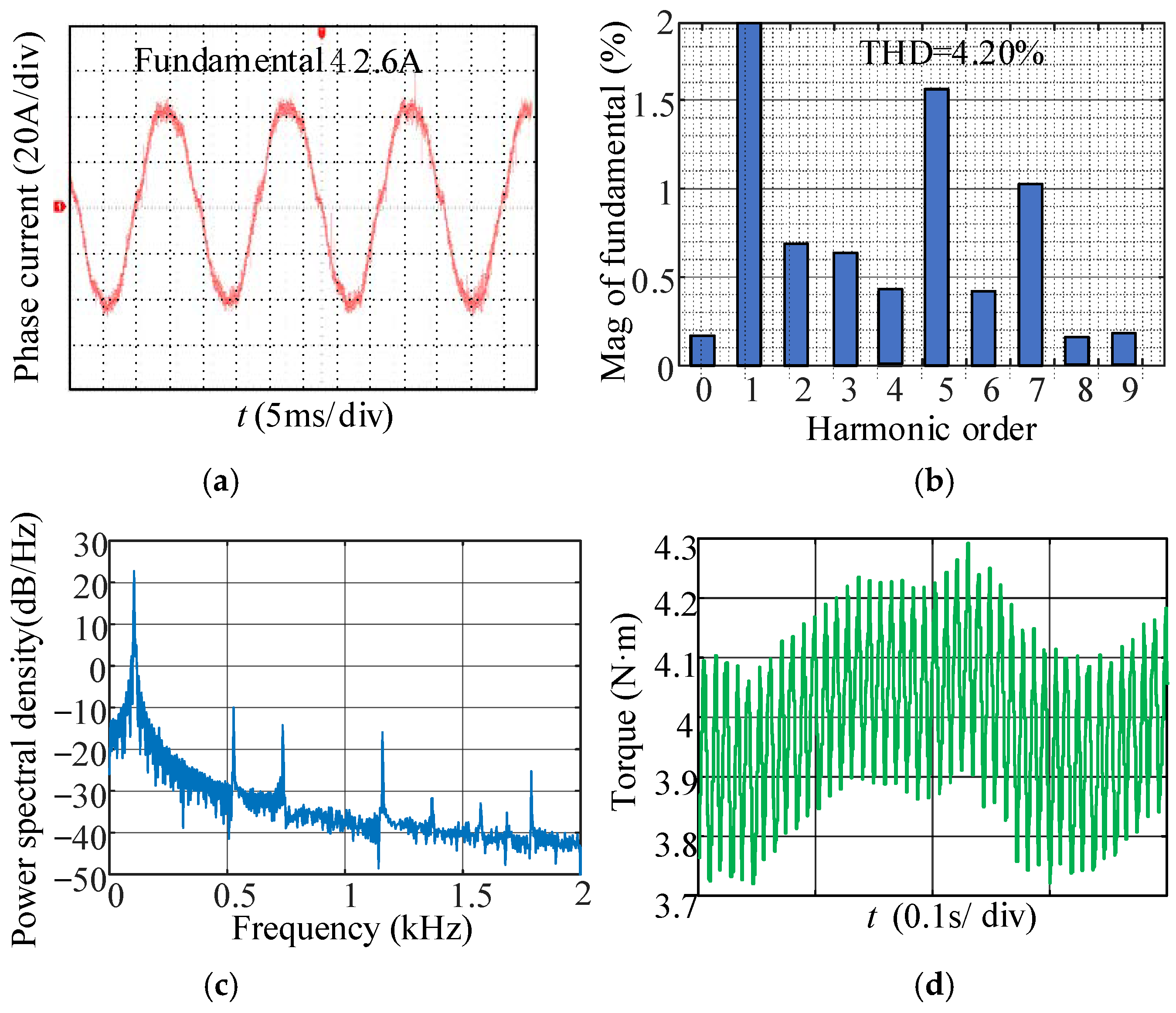
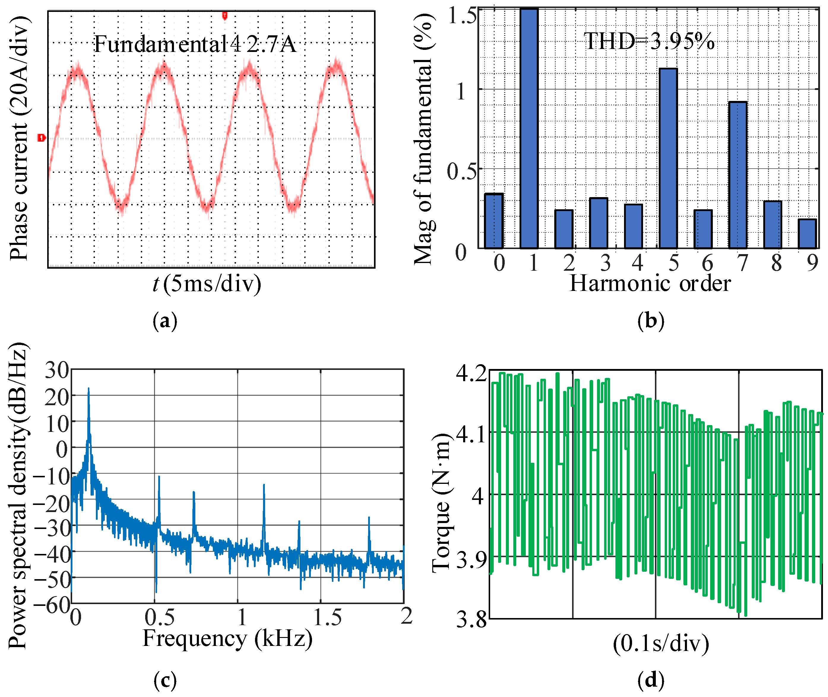
7. Experimental Results and Analysis

The experimental platform as shown in Figure 11 was established to verify the proposed modulation scheme; the models with their parameters or part numbers are listed in Table 1. The DC voltage was supplied by the power supply (PR300-4, MATSUSADA, Shiga, Japan). The three-phase current was detected by the current sensors (MLX91205, MELEXIS, Ieper, Belgium), the speed was detected by the encoder, and the inverter bridge consisted of six IGBT modules (IPB042N10N, Infineon Technologies, Neubiberg, Germany, turn-on time is 1.4 μs, turn-off time is 2.5 μs). The control and modulation algorithm was implemented by the digital signal controller (TMS320-F28035, TEXAS Instruments, Dallas, TX, USA); the switching frequency was 10 kHz.
A closed-loop control model of flux and speed was designed in a two-phase rotating coordinate system (d-q axis), the diagram that contains the field-oriented control detail, is shown in Figure 12. It is a two closed-loop control system. Two PI controllers control the speed (ωr) and the rotor flux (ψr) to eliminate the steady-state errors, and the references of the phase current ( i sd and i sq ) in d-q axis are obtained. Then, the current inner loop adopts two PI controllers to obtain the references of the voltage (ud and uq) in the d-q axis. After the Clarke transformation, the references of the voltage (uα and uβ) in the two-phase station coordinate system are obtained and are used as the inputs for the dead-time free modulation strategy proposed in this paper. The amplitude of the rotor flux (ψr) is calculated by the current model, which is expressed as follows:
ψ r = L m 1 + T r s i sd
where Lm represents the magnetic inductance of IM. The angle (θr) of the rotor flux is obtained by integrating the electrical angular frequency. The parameters of the IM are listed in Table 2.

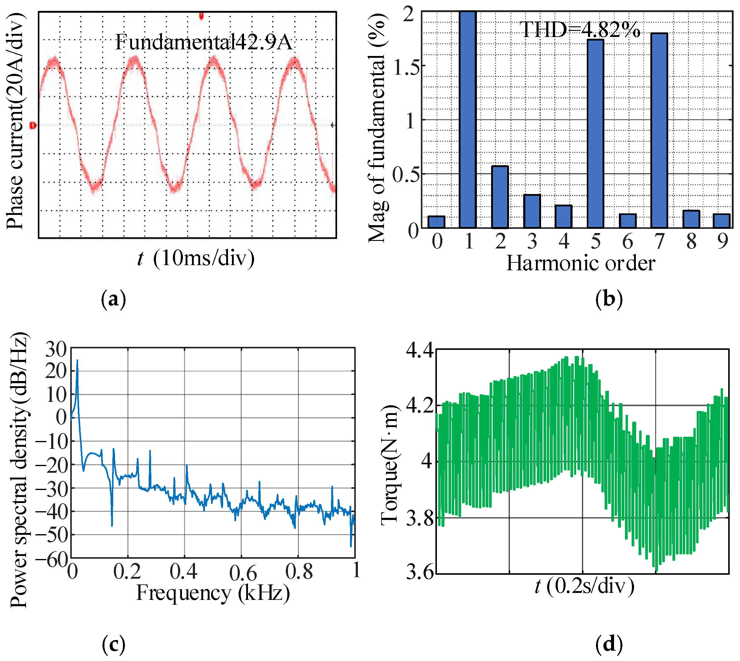
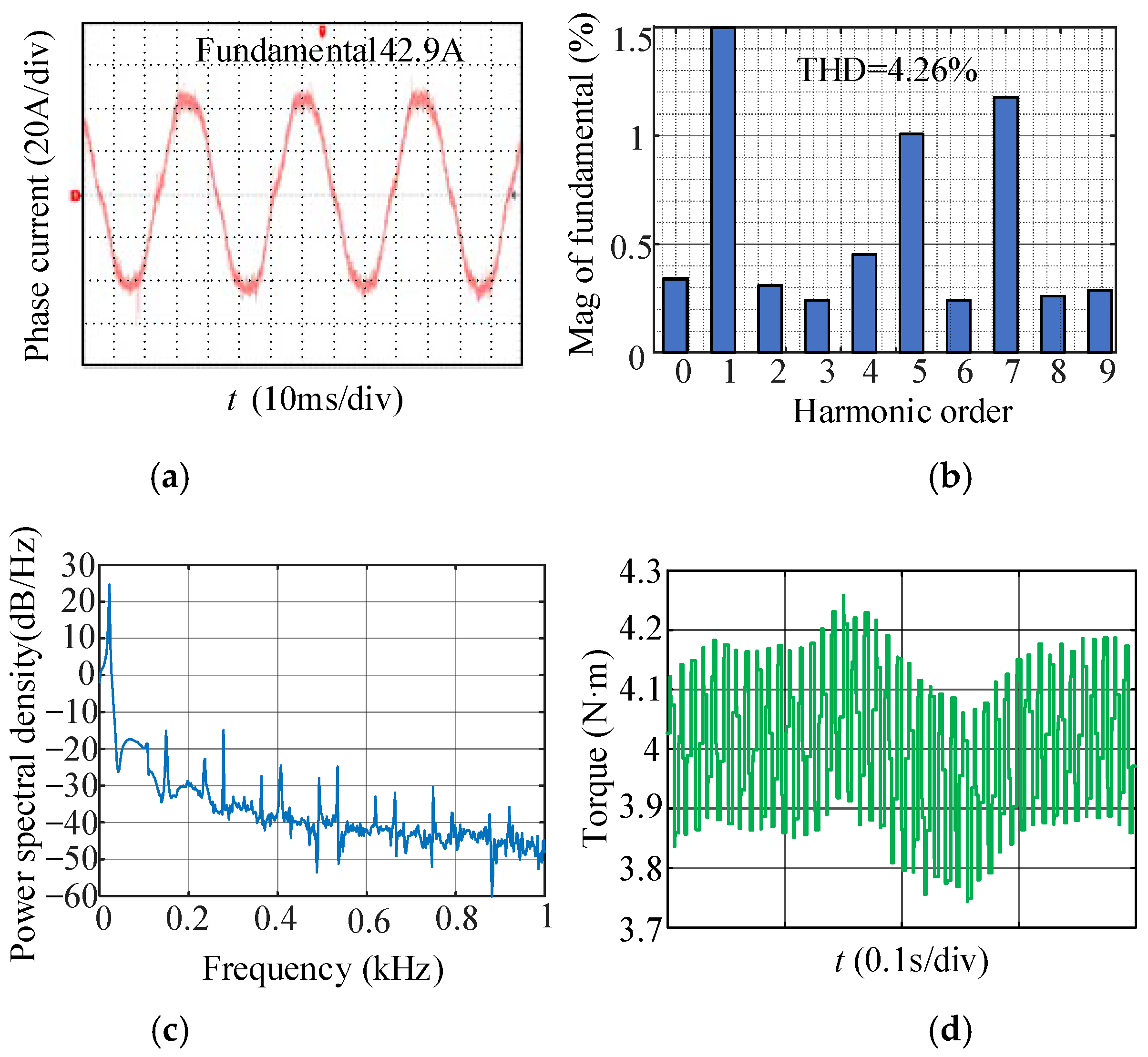
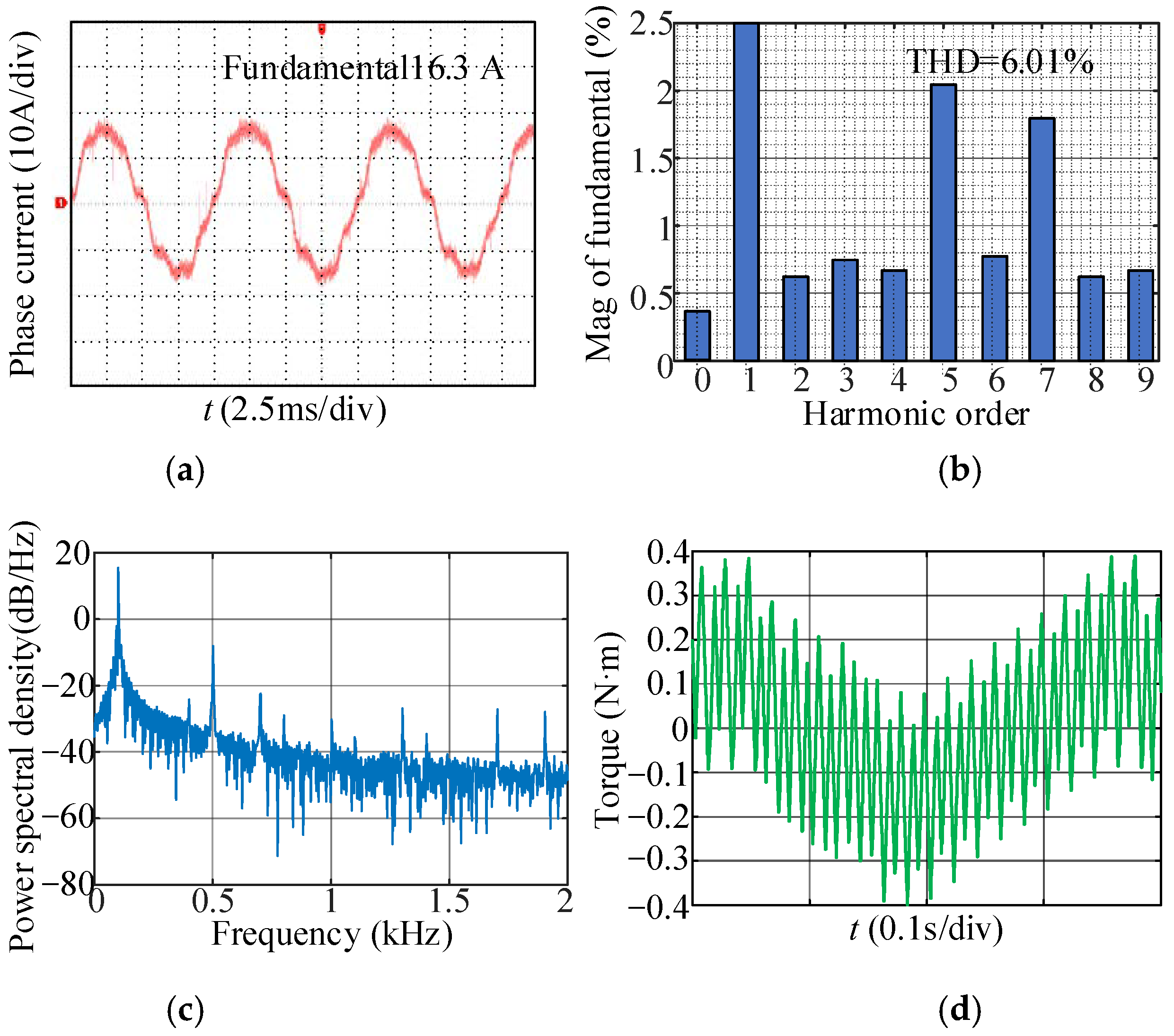
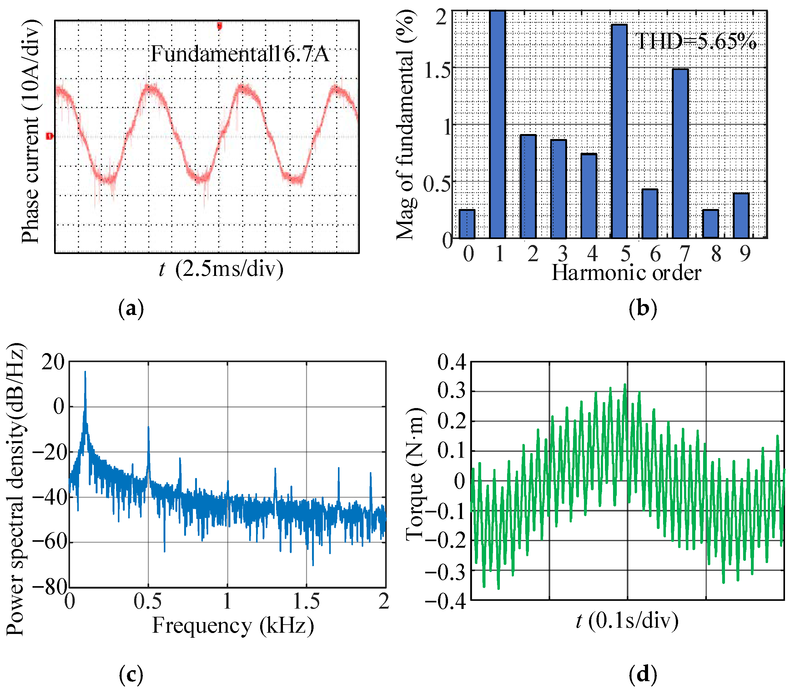
7.1. Experimental Results

Firstly, the effectiveness of the proposed dead-time free modulation scheme was verified when the IM operated at 500 r/min with a load of 4 N·m. Meanwhile, the steady-state performance was compared with the traditional compensation of the pulse duration adopted in [8], and the inverter nonlinearity feedforward compensation proposed in [11]; the experimental results are shown in Figure 13, Figure 14, and Figure 15, respectively. The current was measured by an oscilloscope and the data were saved as a csv file; then, the data were imported into MATLAB R2024a, the FFT analysis results were obtained by executing the corresponding MATLAB instructions. In every control period, the electromagnetic torque was calculated by DSP according to the appropriate equation. The torque data were sent from the DSP to upper computer via the CAN bus at a frequency of 2 kHz; LabVIEW 2023 software stored the data in the form of Excel files. Then, the torque data were imported into MATLAB, and the torque ripple was displayed.
Under the pulse duration compensation, from Figure 13, the THD of the phase current is 4.82%, the torque ripple is ±0.4 N·m, the proportion of the fifth harmonic is 1.74%, and the proportion of the seventh harmonic is 1.79%. The zero current clamping effect is obvious. From Figure 14, it can be seen that after using the nonlinear voltage feedforward compensation method of the inverter, the THD of the phase current is 4.26%, the torque ripple is ±0.25 N·m, the fifth harmonic accounts for 1.01%, and the seventh harmonic accounts for 1.19%. The zero current clamping effect has been improved but still exists. From Figure 15, since the dead-time is eliminated, the steady-state performance is better than those under the other two methods. The THD is reduced to 3.75%, the torque ripple is ±0.2 N·m, the proportion of the fifth harmonic is 0.92%, and the proportion of the sevneth harmonic is 1.03%. Since the phase current can cross zero in advance, the zero current clamping effect has been significantly suppressed.
Then, the operating condition is changed, the IM operates at 3000 r/min without load. The experimental results under the pulse duration compensation adopted in [8], the inverter nonlinearity feedforward compensation proposed in [11], and the proposed dead-time free modulation are shown in Figure 16, Figure 17, and Figure 18, respectively. Under the pulse duration compensation, the THD of the phase current is 6.01%, the torque ripple is ±0.4 N·m, the proportion of the fifth harmonic is 2.04%, and the proportion of the seventh harmonic is 1.8%. Under the nonlinear voltage feedforward compensation method of the inverter, the THD of the phase current is 5.65%, the torque ripple is ±0.35 N·m, the proportion of the fifth harmonic is 1.88%, and the proportion of the seventh harmonic is 1.48%. Under the proposed dead-time free modulation, the THD of the phase current is 4.38%, the torque ripple is ±0.25 N·m, the proportion of the fifth harmonic is 1.55%, and the proportion of the seventh harmonic is 1.09%.
Finally, the operating condition is changed, the IM operates at the rated condition (1500 r/min and 4 N·m). The experimental results under the pulse duration compensation adopted in [8], inverter nonlinearity feedforward compensation proposed in [11], and the proposed dead-time free modulation are shown in Figure 19, Figure 20, and Figure 21, respectively. Under the pulse duration compensation, the THD of the phase current is 4.2%, the torque ripple is ±0.3 N·m, the proportion of the fifth harmonic is 1.58%, and the proportion of the seventh harmonic is 1.03%. Under the nonlinear voltage feedforward compensation method of the inverter, the THD of the phase current is 3.95%, the torque ripple is ±0.2 N·m, the proportion of the fifth harmonic is 1.13%, and the proportion of the seventh harmonic is 0.91%. Under the proposed dead-time free modulation, the THD of the phase current is 3.66%, the torque ripple is ±0.15 N·m, the proportion of the fifth harmonic is 0.89%, and the proportion of the seventh harmonic is 0.54%.
The experimental results under the above two operating conditions indicate that the dead-time free modulation proposed in this paper can achieve better steady-state performance. Meanwhile, on the premise of accurately sampling the phase current in real-time, the two proposed modulation schemes with the switching principle are correct and feasible.

7.2. Discussion and Analysis of the Experimental Results

Firstly, the relationship between voltage harmonics, current harmonics, and torque ripple is discussed. According to Reference [19], in an ideal situation, the line voltage using SVPWM modulation only contains the fundamental and the high-order harmonics near the fundamental frequency, so the phase current has little low-order harmonic, and the frequency of torque ripple is consistent with the switching frequency. However, the nonlinear factors such as dead-time and tube conduction voltage drop will generate the fifth and seventh harmonics of the output voltage, which leads to the fifth and seventh harmonics occurring in the phase current, and the sixth ripple occurring in the torque.
Traditional compensation methods consider the dead-time, turn-on delay, turn-off delay, and conduction voltage drop of the switching tube and diode to compensate for pulse duration, but the compensation accuracy is not high, so the steady-state performance of the IM is the worst. The inverter nonlinearity feedforward compensation proposed in [11] decomposes the voltage error into two parts (∆Van_cond and ∆Van_dt), ∆Van_cond is caused by the conduction voltage drop, and ∆Van_dt is formed in the dead-time stage. Its calculation model is expressed as follows:
{ Δ V an _ cond = V s sign ( i a ) Δ V an _ dt = 2 π V dt atan ( k dt i a )
The conduction voltage drop Vs does not change significantly with the temperature and can be set as a constant according to the data manual. Vdt represents the voltage error caused by the dead-time, and kdt is related to the parameters of the snubber capacitor, which requires multiple experimental tests to be obtained. ∆Van_cond and ∆Van_dt are compensated to the voltage references on the d-q axis.
The diagram of the inverter nonlinearity feedforward compensation is shown in Figure 22, when ia > 0, where V an represents the ideal voltage under SVPWM in a switching period, Van is the actual voltage considering dead-time, turn-on delay, turn-off delay, and conduction voltage drop of the switching tube and body diode. Van_com represents the output voltage after nonlinear voltage feedforward compensation. ΔVan represents the voltage error between V an and Van_com. Although the average error can be eliminated by the nonlinear voltage feedforward compensation, two pulses occur in the waveform of ΔVan in every switching period, which leads to the low-order harmonics in the phase current. In addition, due to the existence of the dead-time, the zero current clamping effect cannot be suppressed significantly.
Due to the elimination of the dead-time, the output voltage Van under the proposed dead-time free modulation has few differences from the ideal voltage V an , and the zero current clamping effect can be suppressed by making the phase current crossing zero in advance. Therefore, in the comparative experiment results of the above three operating conditions, the best steady-state performance of the IM can be obtained by the proposed dead-time free modulation.

8. Conclusions

To reduce the harmonic distortion and torque ripple caused by the dead-time, a novel dead-time free modulation scheme is proposed in this paper. Utilizing the freewheeling characteristics of the body diodes, only one switching tube remains action state in one phase leg, and another one remains off-state. To suppress the zero current clamping effect when the phase current crosses zero, another modulation scheme for the phase current crossing zero in advance is proposed. The dead-time is eliminated during all switching periods. Finally, the feasibility and effectiveness are verified by experiments, and the following conclusion are formed:
(1)
In the non-zero crossing region of the phase current, due to only one tube in the upper and lower bridge arms being in action, the deadtime is eliminated. The nonlinear error between the actual output voltage and the ideal voltage is very little, so the fifth and seventh harmonics of the output voltage can be reduced from the root. The fifth and seventh harmonics and the THD in the phase current under the proposed dead-time free modulation are less than those under other compensation schemes, and the torque ripple minimization can be achieved;
(2)
Near the zero crossing point, the inverter remains in the switching state that can output the maximum voltage whose polarity is the same as the changing direction of the phase current, which accelerates the phase current crossing zero. Compared to other compensation schemes, this method is more effective in suppressing the zero current clamp effect, and the dead-time is avoided.

Author Contributions

Conceptualization, Q.X.; Methodology, L.L.; LabVIEW 2023 Software, X.L.; Validation, X.L. and Y.M.; Investigation, Q.X.; Data curation, X.L.; Writing—original draft, L.Y.; Writing—review & editing, L.L.; Project administration, Y.M.; Funding acquisition, L.L. All authors have read and agreed to the published version of the manuscript.

Funding

This work was supported in part by the Chongqing City Natural Science Foundation Project: CSTB2022NSCQ-MSX0430.

Data Availability Statement

The original contributions presented in the study are included in the article, further inquiries can be directed to the corresponding author.

Conflicts of Interest

The authors declare no conflicts of interest.

References

  1. Payarou, T.; Pillay, P. Integrated Multipurpose Power Electronics Interface for Electric Vehicles. IEEE Trans. Transp. Electrif. 2023, 9, 2429–2443. [Google Scholar] [CrossRef]
  2. Nezamuddin, O.N.; Nicholas, C.L.; Santos, E.C.D. The Problem of Electric Vehicle Charging: State-of-the-Art and an Innovative Solution. IEEE Trans. Intell. Transp. Syst. 2022, 23, 4663–4673. [Google Scholar] [CrossRef]
  3. Dong, Z.; Song, Z.; Wang, W.; Liu, C. Improved Zero-Sequence Current Hysteresis Control-Based Space Vector Modulation for Open-End Winding PMSM Drives with Common DC Bus. IEEE Trans. Ind. Electron. 2023, 70, 10755–10760. [Google Scholar] [CrossRef]
  4. Diao, N.; Sun, X.; Song, C.; Zhang, Q.; Zhang, Z. A Multimodulation Times SVPWM for Dead-Time Effect Elimination in Three-Level Neutral Point Clamped Converters. IEEE Trans. Ind. Electron. 2021, 68, 5476–5485. [Google Scholar] [CrossRef]
  5. Zhou, Y.; Wang, Z.; Xin, G.; Yuan, J.; Shi, X. Dead Time Optimization for Synchronous Switching of SiC MOSFETs Considering Nonlinear Gate Capacitance. IEEE Trans. Power Electron. 2023, 38, 5665–5669. [Google Scholar] [CrossRef]
  6. Arandhakar, S.; Jayaram, N.; Shankar, Y.R.; Gaurav; Kishore, P.S.V.; Halder, S. Emerging Intelligent Bidirectional Charging Strategy Based on Recurrent Neural Network Accosting EMI and Temperature Effects for Electric Vehicle. IEEE Access 2022, 10, 121741–121761. [Google Scholar] [CrossRef]
  7. Feng, W.; Zhang, W.; Huang, S. A Novel Parameter Estimation Method for PMSM by Using Chaotic Particle Swarm Optimization with Dynamic Self-Optimization. IEEE Trans. Veh. Technol. 2023, 72, 8424–8432. [Google Scholar] [CrossRef]
  8. Hwang, S.H.; Kim, J.M. Dead time compensation method for voltage-fed PWM inverter. IEEE Trans. Energy Convers. 2010, 25, 1–10. [Google Scholar] [CrossRef]
  9. Zhang, Z.; Xu, L. Dead-Time Compensation of Inverters Considering Snubber and Parasitic Capacitance. IEEE Trans. Power Electron. 2014, 29, 3179–3187. [Google Scholar] [CrossRef]
  10. Xu, C.; Liu, P.; Liu, T.; Miao, Y.R. Overlap Time Compensation and Characteristic Analysis for Current Source Photovoltaic Grid-Connected Inverter. Energies 2024, 17, 1768. [Google Scholar] [CrossRef]
  11. Lee, J.-H.; Sul, S.-K. Inverter Nonlinearity Compensation Through Deadtime Effect Estimation. IEEE Trans. Power Electron. 2021, 36, 10684–10694. [Google Scholar] [CrossRef]
  12. Wang, L.; Xu, J.; Chen, Q.; Chen, Z.; Huang, R. An Improved Trapezoidal Voltage Method for Dead-Time Compensation in Three-Phase Voltage Source Converter. IEEE Trans. Power Electron. 2022, 37, 8785–8789. [Google Scholar] [CrossRef]
  13. Liao, Y.; Zhen, S.; Liu, R.; Yao, J. Torque ripple suppression of permanent magnet synchronous motor by the harmonic injection. Proc. CSEE 2011, 31, 119–127. [Google Scholar]
  14. Song, P.Y.; Liu, Y.H.; Liu, T.; Wang, H.; Wang, L. A Novel Suppression Method for Low-Order Harmonics Causing Resonance of Induction Motor. Machines 2022, 10, 1206. [Google Scholar] [CrossRef]
  15. Xu, Y.; Zheng, B.; Wang, G.; Yan, H.; Zou, J. Current Harmonic Suppression in Dual Three-Phase Permanent Magnet Synchronous Machine with Extended State Observer. IEEE Trans. Power Electron. 2020, 35, 12166–12180. [Google Scholar] [CrossRef]
  16. Hu, M.; Hua, W.; Cheng, C.; Wang, Y.; Lu, C. Discrete-Time Frequency-Domain Disturbance Observer to Mitigate Harmonic Current in PMSM Drives and the Implementation with Reduced Delay. IEEE Trans. Power Electron. 2023, 38, 9482–9493. [Google Scholar] [CrossRef]
  17. Choi, C.-H.; Seok, J.-K. Pulsating Signal Injection-Based Axis Switching Sensorless Control of Surface-Mounted Permanent-Magnet Motors for Minimal Zero-Current Clamping Effects. IEEE Trans. Ind. Appl. 2008, 44, 1741–1748. [Google Scholar] [CrossRef]
  18. Xu, F.; Liu, J.; Zhang, X. Analysis of Deadtime Effects and Optimum Deadtime Control for Bidirectional Inductive Power Transfer Converters. IEEE Trans. Ind. Electron. 2024, 71, 6929–6937. [Google Scholar] [CrossRef]
  19. Feng, W.; Zhang, W.; Miao, Y.; Huang, S.; Yang, S. Low Frequency Resonance Reduction Method of Induction Motor Used by Electric Vehicle Based on Sixth Harmonic Suppression in dq Coordinate. Trans. China Electrotech. Soc. 2023, 38, 6632–6645. [Google Scholar]
Figure 1. Topology of the induction motor drive system fed by VSI.
Energies 17 03845 g001
Figure 2. Single phase leg configuration of VSI.
Energies 17 03845 g002
Figure 3. Dead-time effects on the output voltage.
Energies 17 03845 g003
Figure 4. Diagram of the zero current clamping effect. (a) Driving signal of upper leg. (b) Driving signal of lower leg. (c) voltage vao between point a and point o. (d) Ideal current and real current.
Energies 17 03845 g004
Figure 5. Modulation diagram of dead-time elimination.
Energies 17 03845 g005
Figure 6. Diagram of the phase current crossing zero in advance.
Energies 17 03845 g006
Figure 7. Diagram of modulation switching within a fundamental period. (a) Description of current changes. (b) State transition diagram.
Energies 17 03845 g007
Figure 8. Bode plot of filter transfer function.
Energies 17 03845 g008
Figure 9. The waveforms of the phase current before and after digital filter.
Energies 17 03845 g009
Figure 10. The flow chart of the modulation selection based on the digital filter.
Energies 17 03845 g010
Figure 11. Experimental platform.
Energies 17 03845 g011
Figure 12. Diagram of the closed-loop control system.
Energies 17 03845 g012
Figure 13. Experimental waveforms under compensation of the pulse duration when IM operates at 500 r/min and 4 N·m. (a) Phase current. (b) Harmonic analysis results. (c) Power spectral density. (d) Torque.
Energies 17 03845 g013
Figure 14. Experimental waveforms under inverter nonlinearity feedforward compensation when IM operates at 500 r/min and 4 N·m. (a) Phase current. (b) Harmonic analysis results. (c) Power spectral density. (d) Torque.
Energies 17 03845 g014
Figure 15. Experimental waveforms under proposed dead-time free modulation when IM operates at 500 r/min and 4 N·m. (a) Phase current. (b) Harmonic analysis results. (c) Power spectral density. (d) Torque.
Energies 17 03845 g015
Figure 16. Experimental waveforms under compensation of the pulse duration when IM operates at 3000 r/min and 0 N·m. (a) Phase current. (b) Harmonic analysis results. (c) Power spectral density. (d) Torque.
Energies 17 03845 g016
Figure 17. Experimental waveforms under inverter nonlinearity feedforward compensation when IM operates at 3000 r/min and 0 N·m. (a) Phase current. (b) Harmonic analysis results. (c) Power spectral density. (d) Torque.
Energies 17 03845 g017
Figure 18. Experimental waveforms under proposed dead-time free modulation when IM operates at 3000 r/min and 0 N·m. (a) Phase current. (b) Harmonic analysis results. (c) Power spectral density. (d) Torque.
Energies 17 03845 g018
Figure 19. Experimental waveforms under compensation of the pulse duration when IM operates at 1500 r/min and 4 N·m. (a) Phase current. (b) Harmonic analysis results. (c) Power spectral density. (d) Torque.
Energies 17 03845 g019
Figure 20. Experimental waveforms under inverter nonlinearity feedforward compensation when IM operates at 1500 r/min and 4 N·m. (a) Phase current. (b) Harmonic analysis results. (c) Power spectral density. (d) Torque.
Energies 17 03845 g020
Figure 21. Experimental waveforms under proposed dead-time free modulation when IM operates at 1500 r/min and 4 N·m. (a) Phase current. (b) Harmonic analysis results. (c) Power spectral density. (d) Torque.
Energies 17 03845 g021
Figure 22. The diagram of the inverter nonlinearity feedforward compensation.
Energies 17 03845 g022
Table 1. Modules and parameters of the experimental platform.
CategoryPart NumberParameters
DC power supplyPR300-472 V
Switching tubes (IGBT)IPB042N10N100 V/100 A
Current sensorsMLX91205/
Digital signal controllerTMS320F28035/
EncoderOIH2500 C/T
Table 2. Parameters of IM and IGBT.
ParametersValue
Rated voltage/frequence/power72 V/50 Hz/1.5 kW
Rated torque/speed4 N·m/1500 r/min
Stator resistance, rotor resistance0.047 Ω, 0.028 Ω
Stator leakage inductance, rotor leakage inductance81.46 μH, 81.27 μH
Magnetic inductance2.29 mH
Moment of inertia0.0164 kg·m2
Number of pole pairs2
Tube conduction voltage drop0.5 V
Body diode conduction voltage drop0.7 V
Disclaimer/Publisher’s Note: The statements, opinions and data contained in all publications are solely those of the individual author(s) and contributor(s) and not of MDPI and/or the editor(s). MDPI and/or the editor(s) disclaim responsibility for any injury to people or property resulting from any ideas, methods, instructions or products referred to in the content.

