Article

An Improved Cascaded Boost Converter with an Ultra-High Voltage Gain Suitable for Dielectric Quality Tests

1
School of Electrical and Computer Engineering, University of Tehran, Tehran 1417935840, Iran
2
Electrical Engineering Faculty, Islamic Azad University, Tehran 1477893855, Iran
3
Electrical Engineering Faculty, University of New Brunswick, Fredericton, NB E3B 5A3, Canada
*
Author to whom correspondence should be addressed.
Energies 2024, 17(15), 3861; https://doi.org/10.3390/en17153861
Submission received: 30 June 2024 / Revised: 28 July 2024 / Accepted: 31 July 2024 / Published: 5 August 2024
(This article belongs to the Section F: Electrical Engineering)

Abstract

:
Dielectric quality tests require a high AC voltage with a frequency range of 0.0001 Hz to 1000 Hz. However, providing a high AC voltage with such a frequency variety is challenging. Providing a high DC voltage and then applying such a voltage to an inverter to adjust the frequency can be an acceptable solution for such a challenge. Notably, a high DC voltage is required for DC tests. This study proposes an improved form of the cascaded boost converter, whose merits are as follows: (i) the high voltage gain providing low duty cycles is possible; (ii) the input current is continuous, which decreases the current ripple of the input filter capacitor; (iii) the current stress of the semiconductors is less than the input current, and most of them have a large difference with it; (iv) the voltage stress of the semiconductors is less than the output voltage with a large difference; (v) only one switch with a simple drive circuit is used; (vi) the common ground of the load and input source decreases the EMI noise; (vii) besides the high voltage gain, the voltage density of the converter based on the number of inductors, capacitors, switches, diodes, and whole components is greater than that of the recently proposed converters; (viii) only two stacked connections of the proposed topology can provide a 2.6 kV voltage for a higher DC voltage test of dielectrics. The functional details of the converter are extracted in ideal and continuous conduction (CCM) modes. Moreover, the converter’s voltage gain and density are compared with the recently proposed converters to show the superiority of the proposed converter. Finally, the experimental results are presented to validate the theoretical relations in a 140 W output power.

1. Introduction

Isolated DC–DC converters employ high-frequency transformers to achieve high voltage gain values [1]. The coil’s turn ratio plays an essential role in increasing voltage gain [2]. However, employing isolated DC–DC converters increases the converters’ volume and mass [3]. Moreover, the load isolation from the input source leads to EMI noises. Additionally, the coils’ leakage inductance and residual current cause issues during the switch’s inactivation. In other words, a considerable voltage stress is applied to the switch, which can cause its failure [4]. Solving such a problem requires using the snubber circuits to dissipate the loss of the residual currents in an unimportant part [5,6]. Using the snubbers does not change the efficiency but increases the converter’s complexity [7]. Moreover, the input current of the isolated converters is discontinuous, which increases the current stress of the input filter capacitor [8]. All these concepts lead to the use of non-isolated DC–DC converters in such an application, which does not require the isolation of the load and input source [9].
Among classic non-isolated DC–DC converters, boost topology is the most popular one. It has a continuous input current with a negligible ripple. The common ground of the load and input source is provided. Consequently, the EMI noise problems are solved. The employed switch is low-sided with a simple drive circuit. Finally, the converter has a step-up behavior in all duty cycles. Besides all the mentioned advantages, there are some disadvantages with this topology. The first disadvantage is the voltage stress of the semiconductors in this topology. Notably, the voltage stress of the semiconductors is the same as the output voltage. In other words, an increase in output voltage leads to an increase in voltage stress. The second problem is the lack of high voltage gain providing. As the duty cycle approaches 80%, the voltage gain of the boost topology increases five-fold. Additionally, a 10-times voltage gain requires a 90% duty cycle. It can be understood that the higher voltage gain values lead to the duty cycle approaching unity. However, employing such a duty cycle is not possible. In other words, using a duty cycle close to unity decreases the conduction time of the diode to zero. However, the physical limits of the diodes do not allow for such a condition. Moreover, in a practical mode, the duty cycle approaching unity does not lead to the voltage gain’s increase due to the parasitic elements of the circuit components. Consequently, such a converter cannot provide a high voltage gain. A simple way to increase the voltage gain is the cascaded connection of two boost converters. Figure 1a presents the power circuit of the cascaded boost topology. All the advantages of the boost topology are present in this converter. Moreover, its voltage gain is the quadratic form of the boost one. Consequently, it has a higher voltage gain than a boost converter. Notably, the voltage stress of the switch and the last diode in this topology is the same as the output voltage. Consequently, the disadvantage of the boost topology is repeated. Another way to increase the voltage gain of the boost topology is the voltage lift technique. This technique uses diode–capacitor or diode–capacitor–inductor voltage multiplier cells to increase the voltage gain. In this method, a voltage is copied in the capacitors, and in the following operating mode, the capacitors’ voltages are summed up with each other. Figure 1b–e present the improved boost topologies with voltage multiplier cells. The voltage gain provided by the first to third improved boost topologies is twice that of the boost converter. Notably, the voltage gain of the fourth improved boost converter is three times that of the boost one. Besides the voltage gain increase, the voltage stress of the semiconductors is less than the output voltage in the second to fourth improved boost converters. However, the first one has the same disadvantage of the boost and cascaded boost topologies. Figure 2 presents the voltage gain comparison of the boost, cascaded boost, and improved boost topologies. All the improved and cascaded boost converters have a higher voltage gain than the boost one. Additionally, the improved boost topologies function better at low-percentage duty cycles. Moreover, the cascaded boost converter needs a duty cycle higher than 70% to provide a higher voltage gain than the rest. Another common concept about the improved topologies is that all of them require a high percentage of the duty cycle to provide a voltage gain of more than ten times.
The topologies in [10,11,12,13,14,15,16,17,18,19,20,21,22,23,24,25,26,27,28,29,30,31,32,33,34,35,36,37,38,39] combine classic non-isolated DC–DC converters. The presented topologies in [10,19,20,21,23,26,28,29,39] are the combination of buck-boost, Cuk, Sepic, and zeta converters. The function of these converters is acceptable in the step-down or pass-through modes. However, these converters’ step-up mode is unacceptable and cannot provide higher voltage gains. Additionally, their voltage gain is less than the boost converter, while the duty cycle is less than 65%. Furthermore, such a low voltage gain is provided by more components than the classic boost converter. Besides all the mentioned disadvantages, the semiconductors close to the output terminal experience a voltage stress higher than the voltage provided at the output. The presented topologies in [11,12,15,17,27,33,35,37] use a boost topology besides a buck-boost, Cuk, SEPIC, or Zeta converter. Their output voltage is higher than the last group. However, it is not higher than the boost converter in all duty cycles. Consequently, besides using more components than the boost topology, the provided voltage gain is unacceptable. Also, some semiconductors face a voltage more than the output voltage. Another common drawback in the discussed topologies is the use of Cuk, SEPIC, and Zeta converters, which increases the number of components spatially bythe magnetic base components without providing the desired voltage gain and semiconductor voltage stress. The presented topologies in [13,16,25,30,31,32,36,38] are quadratic boost topologies like the cascaded boost topology. However, the number of switches exceeds that of the cascaded boost converter. The voltage stress of the semiconductors has the same condition as in the cascaded boost topology. The presented topologies in [14,40] are the improved form of the Cuk and SEPIC converters. The voltage gain provided is twice that of the Cuk and SEPIC. However, this improvement is not sensible and unacceptable compared with the increase in the number of components. The same idea was employed in [18,22,24]; however, the achievement of [24] is better than the rest. The voltage gain is more than the cascaded boost converter. However, this voltage gain is not more than ten times at the low duty cycle percentages. Ref. [34] presents the stack connection of the boost and buck-boost topologies. The provided voltage gain is the summation of the individual converters. The voltage stresses become less than the output voltage with such a simple method. However, the voltage gain is not as high as desired. The proposed topologies in [40,41,42,43,44,45,46,47,48,49,50,51,52,53,54,55,56,57,58,59,60] use the inductor–diode–capacitor voltage multiplier cells to employ the voltage lift technique. The extracted voltage gain from [41,43] is four times and twice the boost converter. However, they lack the common ground of the load and input source. The number of magnetic-based components in [42] is three times the boost topology. However, the voltage gain does not have a high increase. Ref. [44] employed nine diodes, five inductors, three capacitors, and one switch. However, the provided voltage is almost three times the boost converter at a low duty cycle percentage. Moreover, some semiconductors face a voltage stress higher than the output voltage. Such disadvantages are repeated in [45]. Refs. [46,47] provides the same voltage gain with the same number of components. These converters employ two switches in the power circuit. However, the provided voltage gain is not as high as desired. Ref. [48] is an improved buck-boost topology. Its voltage gain is more than the classic buck-boost one. However, the main drawbacks of the buck-boost topology are present in this converter. Additionally, the magnet-based components are many, which decreases the power density of this topology. Moreover, the increase in voltage gain is not sensible compared with the increase in components. Ref. [49] is an improved form of the SEPIC topology. It uses one inductor, four capacitors, and diodes more than the classic SEPIC topology. However, the voltage gain increase is not bold. Refs. [50,53] combine boost and super lift luo converters. Their voltage gain is more than the cascaded boost topology. Moreover, the voltage stress problem of the cascaded boost topology is solved. However, the extracted voltage gain cannot provide a ten-times voltage gain with low duty cycle percentages. The proposed topologies in [51,52,53,54,55,56,57,58,59,60] are the improved form of the cascaded boost converters. Their voltage gain can be achieved ten times with a low percentage of duty cycles. Moreover, the voltage stress of the semiconductors is less than the output voltage. These features are acceptable for renewable energy applications. However, a high-voltage DC test equipment, which is used in dielectric tests, is not suitable. Moreover, in such applications, low voltage stresses are required to be applied to the components. Consequently, the voltage stresses must be less than the output voltage with a large difference. All these converters are based on the use of the classic converters without using any coupled inductors and transformers. The voltage lift, which is explained at the beginning of this paper, is explained in more detail in [61] for various topologies. One of this technique’s prominent disadvantages is the increase in the number of components. In other words, the voltage gain can be increased by using more inductor–diode cells or more diode–capacitor structures. The first method increases the mass and volume of the converter and decreases the power density. However, using diode–capacitor structures increases the voltage gain without increasing mass and volume. Notably, the capacitors have a lower mass, volume, cost, and loss compared with inductors. The MKT and MKP types of capacitors have a negligible equivalent series resistance (ESR), high capacitance, and high voltage range. Consequently, they can be used for DC links. Unfortunately, the topologies presented in [61] used more inductors, which increased the loss. The application of the converter has an essential effect on converter design. For example, the topologies presented in [62,63,64,65,66,67,68,69,70,71,72,73,74,75,76,77,78,79,80,81,82,83,84,85] are recommended to be used in renewable energy sites such as photovoltaic farms, fuel cells, and hydrogen electrolysis. In these studies, their features in control and employing MMPT methods are prominent, and providing ultra-high gain values is not expected. It is good to mention that renewable energy resources provide a voltage gain of 15 V to 60 V. Consequently, a converter with a ten-times voltage gain can be easily used in such an application. However, the equipment used in dielectric tests is not suitable. Other types of converters are based on the use of a couple of inductors in the power circuit. As with the isolated converters, the turn ratio of the coils appears as a coefficient in the voltage gain and makes the converter independent on using a high percentage of the duty cycle. Moreover, employing the couple inductors can solve the non-minimum phase behavior of the converter. All the topologies presented in [86,87,88,89,90,91,92,93,94,95,96,97,98,99,100,101,102,103,104,105,106,107,108,109,110,111,112,113,114,115,116,117,118,119,120,121,122,123,124,125,126,127,128,129,130,131,132,133,134,135,136,137,138,139,140,141,142] are the newly proposed converters of this type. Unfortunately, using the coupled inductors and their leakage inductances increases the losses and forces high voltage stresses on the converters’ switch. Hence, snubber circuits and extra circuits or procedures are required to solve the mentioned problems and maintain efficiency at higher values. However, employing the mentioned circuits increases the number of components and the complexity of the converter control. Furthermore, a decrease in reliability, according to this happening, is significant. Consequently, employing a couple of inductors in the power circuit causes the same problems as the isolated converters. The topologies in [143,144,145,146,147,148,149,150,151,152,153,154] are topologies based on boost topology that have been presented for renewable applications. According to the mentioned application, ultra-high voltage gain values are not accessible in this group of converters.
This paper proposes an improved cascaded boost topology. The topology of the cascaded boost topology is improved by diode–inductor–capacitor and diode–capacitor voltage multiplier cells. This improvement creates a high-voltage-lift value suitable for high-voltage test applications. There is only one switch in the power circuit. Moreover, as with the boost topology, the continuity of the input current and common ground of the load and input source are present. Notably, besides the high voltage gain value, the voltage stress of the semiconductors is less than the output voltage. In other words, the highest value of the voltage stress is one-third of the output voltage. Consequently, the voltage stress challenge of the conventional boost and cascaded boost is solved in this topology.

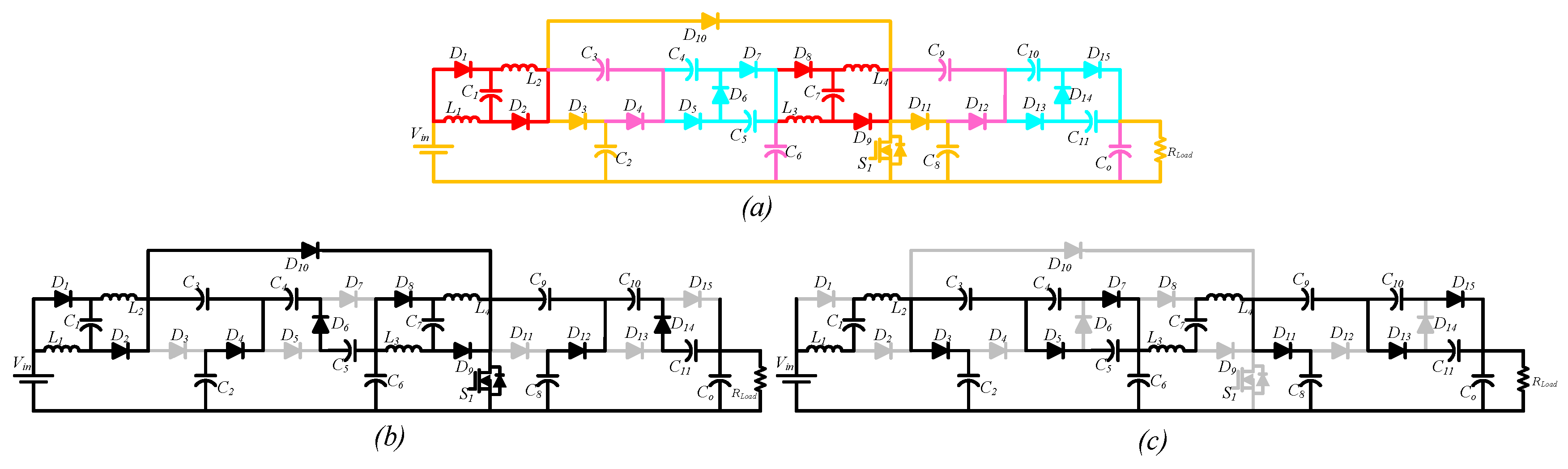
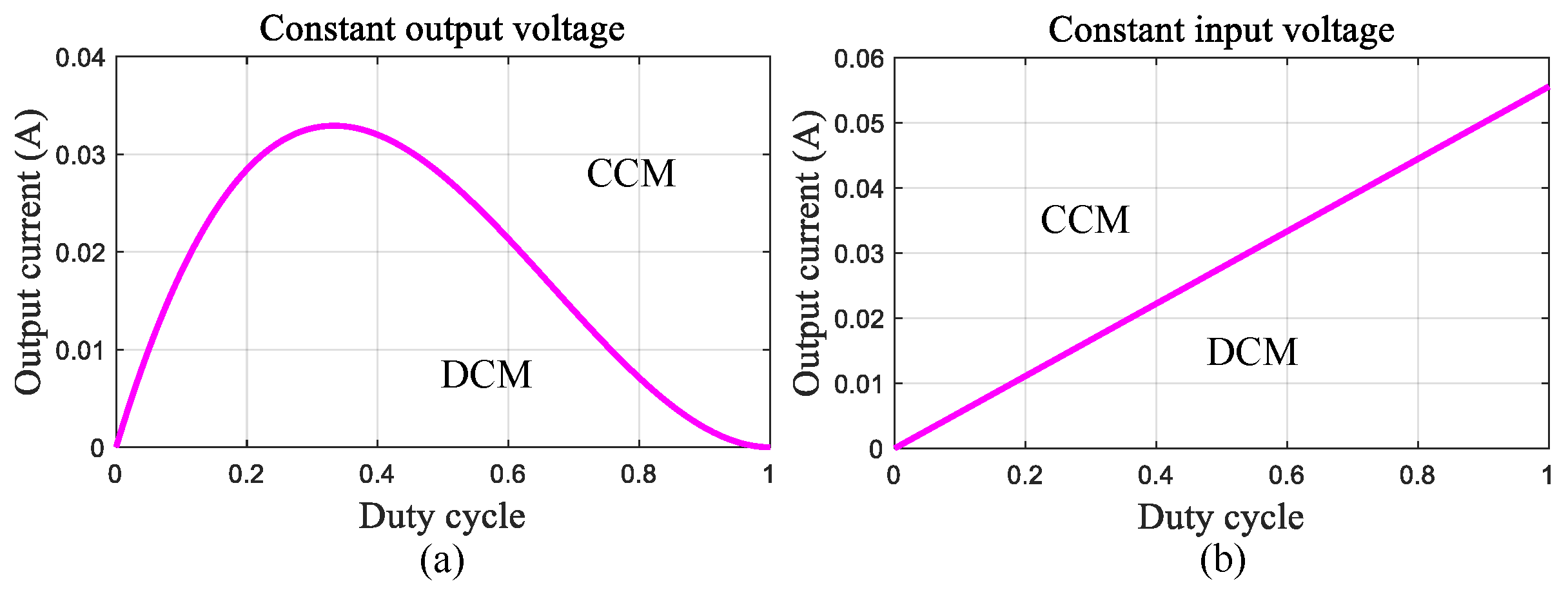
2. Proposed Topology in the Ideal Mode

The proposed topology is presented in Figure 3. According to this figure, two kinds of voltage multiplier cells improve the cascaded boost topology. The beginning part of the boost topologies is modified by an inductor–diode–capacitor voltage multiplier cell. This voltage multiplier cell increases the voltage gain of the boost converter two-fold. The end part of the boost converters is modified by a diode–capacitor voltage multiplier cell. This diode–capacitor voltage multiplier cell increases the boost topology voltage gain three-fold. This topology is a one-switch converter. There are two operational modes for the proposed topology in the ideal mode and the steady state. The equivalent circuit of the first operating mode is shown in Figure 3. According to this figure, the first, second, fourth, sixth, eighth, ninth, tenth, twelfth, and fourteenth diodes beside the switch are activated. According to the equivalent circuit of the converter in this mode, the first capacitor with the input source, the second capacitor with the third one, the sixth capacitor with the seventh one, and the eighth capacitor with the ninth one become parallel with each other. Therefore, their voltages become the same. Additionally, the series connection of the third to fifth capacitors is parallel with the sixth capacitor, and the series connection of the ninth to eleventh capacitors is parallel with the output capacitor. All the applied voltages to the inductors are positive, and all of them become magnetized. The equivalent circuit of the second operating mode is shown in Figure 3c. According to this figure, the third, fifth, seventh, eleventh, thirteenth, and fourteenth diodes are activated. In this circuit, the fourth capacitor with the fifth and the tenth capacitors with the eleventh ones are parallel. Moreover, the series connection of the second to fourth capacitors is parallel with the sixth capacitor and the series connection of the eighth to tenth capacitors with output one. According to the expressed concepts, the voltage equation of the inductors is as follows:
V L 1 = D ( V i n ) + ( 1 D ) ( V i n + V C 1 V ) V L 2 = D ( V i n ) + ( 1 D ) ( V V C 2 ) V L 3 = D ( V C 6 ) + ( 1 D ) ( V C 6 + V C 7 V ) V L 4 = D ( V C 6 ) + ( 1 D ) ( V V C 8 )
In this equation, V′ stands for the common node voltage of the first diode, first capacitor, and second inductor. Additionally, V″ is the common node voltage of the eighth diode, seventh capacitor, and fourth capacitor.
The current equation of the capacitors according to the equivalent circuits and the expressed concepts are as follows:
i C 1 = D ( i 1 ) + ( 1 D ) ( i L 1 ) i C 2 = D ( i 2 ) + ( 1 D ) ( i L 1 i 3 ) i C 3 = D ( i 2 + i 6 ) + ( 1 D ) ( i 3 ) i C 4 = D ( i 6 ) + ( 1 D ) ( i 4 ) i C 5 = D ( i 6 ) + ( 1 D ) ( i 3 + i 4 ) i C 6 = D ( i 6 i 7 i L 3 i L 4 ) + ( 1 D ) ( i 3 i L 3 ) i C 7 = D ( i 7 ) + ( 1 D ) ( i L 3 ) i C 8 = D ( i 8 ) + ( 1 D ) ( i L 3 i 9 ) i C 9 = D ( i 8 + i 12 ) + ( 1 D ) ( i 9 ) i C 10 = D ( i 12 ) + ( 1 D ) ( i 10 ) i C 11 = D ( i 12 ) + ( 1 D ) ( i 9 + i 10 ) i C o = D ( i 12 I o ) + ( 1 D ) ( i C 9 I o )
In this equation, i 1 stands for the inrush current of the first capacitor when it becomes parallel to the input source. i 2 stands for the inrush current of the second capacitor while it is parallel to the third capacitor. Notably, i 6 is the inrush current of the sixth capacitor as it becomes parallel to the series connection of the third to fifth capacitors. i 7 is the inrush current of the seventh capacitor, which becomes parallel to the sixth capacitor. i 8 is the inrush current of the eighth capacitor when it is paralleled to the ninth capacitor. i 12 is the inrush current of the output capacitor as it becomes parallel to the series connection of the ninth to eleventh capacitors. i 3 is the inrush current of the third capacitor while its series connection with the second and fifth capacitors is parallel to the sixth capacitor. i 4 is the inrush current of the fourth capacitor, which becomes parallel to the fifth capacitor. i 9 is the inrush current of the series connection of the eighth, ninth, and eleventh capacitors when it becomes parallel to the output capacitor. i 10 is the created inrush current by the parallel connection of the tenth and eleventh capacitors.
It is good to note that the average voltage of the inductors is zero according to the voltage’s second balance. Consequently, all the Equations in (1) are equal to zero. Based on this fact, the average voltage of the capacitors becomes accessible as follows:
V C 1 = V i n , V C 2 = V C 3 = 2 1 D V i n , V C 3 = V C 4 = V C 5 = 2 1 D V i n V C 6 = V C 7 = 6 1 D V i n , V C 8 = V C 9 = V C 10 = V C 11 = 12 ( 1 D ) 2 V i n , V o = 6 1 D 2 V i n
According to the current’s second balance, the average current of the capacitors is zero. Solving the capacitors’ current equation according to the mentioned concept leads to the inductors’ and inrush currents’ average values as follows:
I L 1 = I L 2 = 18 ( 1 D ) 2 I o , I L 3 = I L 4 = 3 1 D I o , i 1 = 18 D ( 1 D ) I o , i 2 = 6 D ( 1 D ) I o i 3 = 12 ( 1 D ) 2 I o , i 4 = 6 ( 1 D ) 2 I o , i 6 = 6 D ( 1 D ) I o , i 7 = 3 D I o i 8 = I o D , i 9 = 2 1 D I o , i 10 = I o 1 D , i 12 = I o D
According to the extracted relation of the voltage gain, it can be understood that the provided voltage gain by this topology is 36 times more than the conventional cascaded boost topology. Figure 4 presents the voltage gain comparing the boost and cascaded boost topologies with the proposed converter. It can be understood that the voltage gain values provided by the proposed topology at the low-duty cycles are not accessible for the boost and cascaded boost topologies at higher-duty cycles.
According to the extracted values for the capacitors’ voltage, inductors’ current, and capacitors’ inrush currents, the semiconductors’ voltage and current stress are as follows. Notably, the semiconductors’ current stress is the average crossing current from the semiconductors during their activation, and the voltage stress is the peak value of the applied voltage during their inactivation mode.
I S = 35 + 2 D D 2 ( 1 D ) 2 I o , I D 1 = I D 2 = 18 ( 1 D ) 2 I o I D 3 = I D 4 = I D 5 = I D 6 = I D 7 = 6 1 D I o I D 8 = I D 9 = 3 1 D I o , I D 10 = 5 + D 1 D I o I D 11 = I D 12 = I D 13 = I D 14 = I D 15 = I o
V D 1 = V D 2 = V i n 1 D , V D 3 = V D 4 = V D 5 = V D 6 = V D 7 = 2 1 D V i n V D 8 = V D 9 = 6 ( 1 D ) 2 V i n , V S = V D 11 = V D 12 = V D 13 = V D 14 = V D 15 = 12 ( 1 D ) 2 V i n
Figure 5 presents the normalized voltage/current stress of the semiconductors. Notably, the output voltage is the base voltage of voltage stresses. Additionally, the input current is considered as the base current of the current stresses. According to this figure, all the normalized voltage/current stresses are less than unity. Notably, the current stress of the eleventh to fifteenth diodes is the same as the output current, which is the lowest current in this topology. The highest current stress of the diodes belongs to the first and second diodes, which is half of the input current. Furthermore, the highest current stress is for the switch, whose current stress is less than the input current at the maximum duty cycle.
Among the voltage stresses, the tenth to fifteenth diodes and the switch have the highest voltage stress, which is one-third of the output voltage. It can be understood that all the semiconductors have an acceptable condition in this topology.
The simplified form of the inductors’ current ripple and capacitors’ voltage ripple are as follows:
Δ i L 1 = 1 L 1 0 D T s V L 1 ( t ) d t = 1 L 1 0 D f s V L 1 ( t ) d t = D V i n L 1 f s Δ i L 2 = 1 L 2 0 D T s V L 2 ( t ) d t = 1 L 2 0 D f s V L 2 ( t ) d t = D V i n L 2 f s Δ i L 3 = 1 L 3 0 D T s V L 3 ( t ) d t = 1 L 3 0 D f s V L 3 ( t ) d t = 6 D V i n ( 1 D ) L 3 f s Δ i L 4 = 1 L 4 0 D T s V L 4 ( t ) d t = 1 L 4 0 D f s V L 4 ( t ) d t = 6 D V i n ( 1 D ) L 4 f s
Δ V C 1 = 1 C 1 0 D T s i C 1 ( t ) d t = 1 C 1 0 D f s i C 1 ( t ) d t = 18 I o ( 1 D ) C 1 f s Δ V C 2 = 1 C 2 0 D T s i C 2 ( t ) d t = 1 C 2 0 D f s i C 2 ( t ) d t = 6 I o ( 1 D ) C 2 f s Δ V C 3 = 1 C 3 0 D T s i C 3 ( t ) d t = 1 C 3 0 D f s i C 3 ( t ) d t = 12 I o ( 1 D ) C 3 f s Δ V C 4 = 1 C 4 0 D T s i C 4 ( t ) d t = 1 C 4 0 D f s i C 4 ( t ) d t = 6 I o ( 1 D ) C 4 f s Δ V C 5 = 1 C 5 0 D T s i C 5 ( t ) d t = 1 C 5 0 D f s i C 5 ( t ) d t = 6 I o ( 1 D ) C 5 f s Δ V C 6 = 1 C 6 0 D T s i C 6 ( t ) d t = 1 C 6 0 D f s i C 6 ( t ) d t = 3 ( 3 + D ) I o ( 1 D ) C 6 f s Δ V C 7 = 1 C 7 0 D T s i C 7 ( t ) d t = 1 C 7 0 D f s i C 7 ( t ) d t = 3 I o C 7 f s Δ V C 8 = 1 C 8 0 D T s i C 8 ( t ) d t = 1 C 8 0 D f s i C 8 ( t ) d t = I o C 8 f s Δ V C 9 = 1 C 9 0 D T s i C 9 ( t ) d t = 1 C 9 0 D f s i C 9 ( t ) d t = 2 I o C 9 f s Δ V C 10 = 1 C 10 0 D T s i C 10 ( t ) d t = 1 C 10 0 D f s i C 10 ( t ) d t = I o C 10 f s Δ V C 11 = 1 C 11 0 D T s i C 11 ( t ) d t = 1 C 11 0 D f s i C 11 ( t ) d t = I o C 11 f s Δ V o = 1 C o 0 D T s i C o ( t ) d t = 1 C o 0 D f s i C o ( t ) d t = ( 1 + D ) I o C o f s
The converter’s operation in the continuous conduction mode (CCM) stands for the inductors’ current ripple and inductors’ average current. The inductors’ current ripple has a reversed relation with inductance. Notably, the inductors’ current ripple must be more than twice the corresponding inductor average current to provide the CCM. According to this concept, the inductors’ minimum value is as follows:
L 1 D ( 1 D ) 4 R 1296 f S , L 2 D ( 1 D ) 4 R 1296 f S , L 3 D ( 1 D ) 2 R 36 f S , L 4 D ( 1 D ) 2 R 36 f S
The inductors’ average current is the second factor of the converters operating in CCM.The inductors’ average current must be more than half of the corresponding inductor’s current ripple. The inductors’ average current depends on the output average current and duty cycle. Figure 6 presents the operational region of the converter among CCM, DCM, and boundary conditions according to the output average current and duty cycle for a constant output voltage and a constant input voltage. The employed relations for the mentioned figure are as follows:
I O B = V O 36 L 4 f s D ( 1 D ) 2 I O B = V i n L 4 f s D
Any point up the mentioned curves in Figure 6 belongs to CCM. Additionally, any point under the mentioned curves is for DCM. Finally, any point on the curve is the boundary condition.

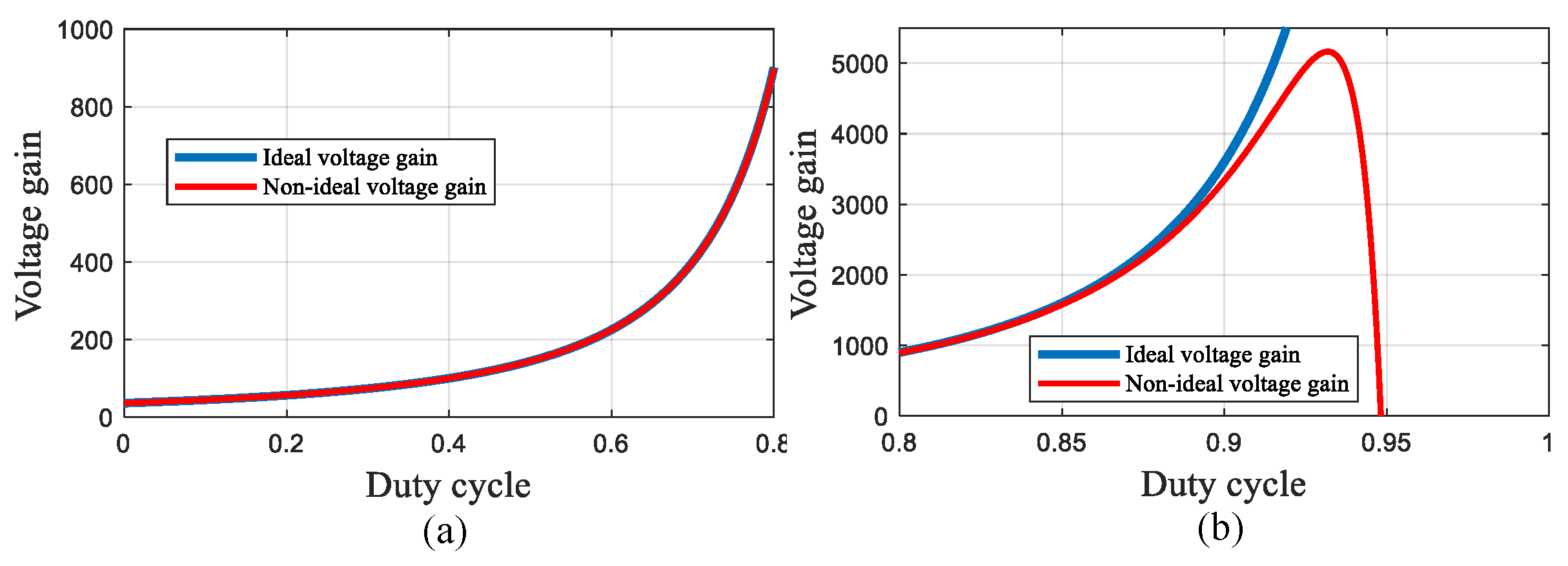
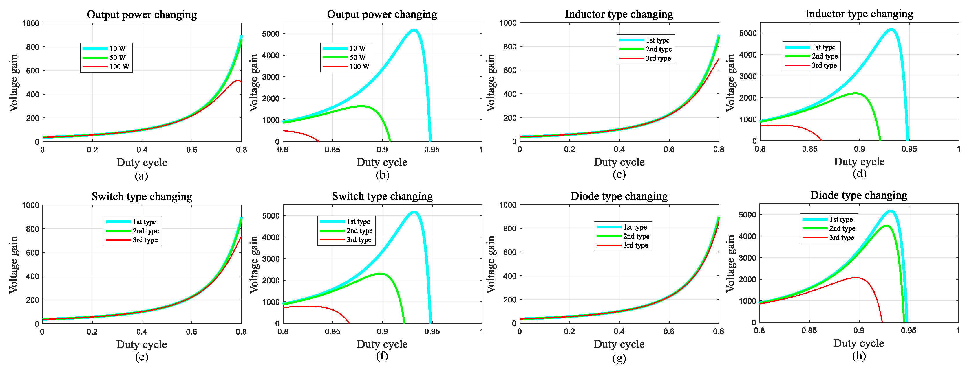
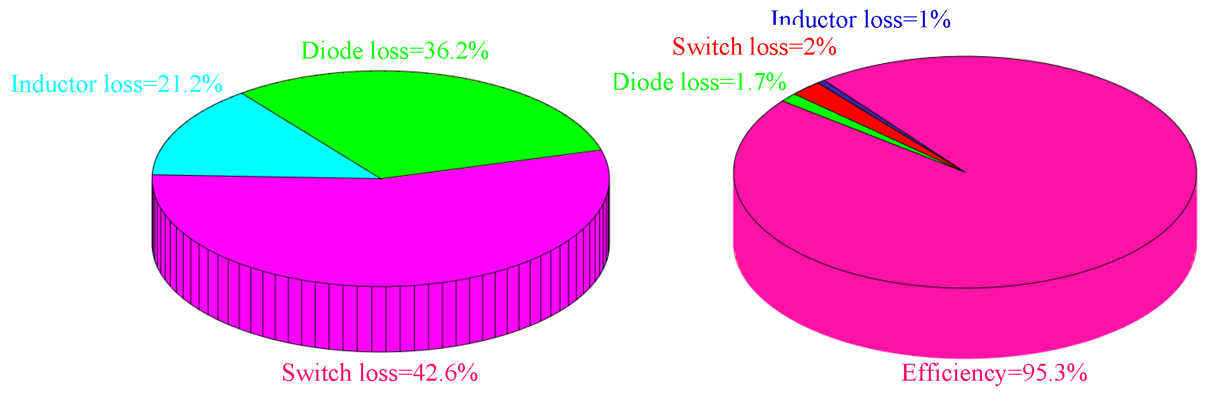
3. Non-Ideal Voltage Gain and Efficiency

The extracted relation of the voltage gain in the second section is for the ideal mode, where the equivalent series resistance of the inductor ( r L ), switch ( r S ), diode ( r D ), and load (R) are absent. Considering the mentioned parameters, the voltage gain of the boost converter is as follows in the non-ideal mode.
v o V i n = 1 ( 1 D ) 1 r L R 1 ( 1 D ) 2 r S R D ( 1 D ) 2 r D R 1 ( 1 D )
For the cascaded boost topology, we have
v o V i n = 1 ( 1 D ) 2 1 r L R 1 ( 1 D ) 4 r S R D ( 1 D ) 4 r D R 1 ( 1 D ) 3
Applying the effect of the voltage multiplier cells to the relation, the non-ideal voltage gain relation of the proposed topology becomes as follows:
v o V i n = 36 ( 1 D ) 2 1 r L R 36 ( 1 D ) 4 r S R 36 D ( 1 D ) 4 r D R 36 ( 1 D ) 3
According to the extracted relation, the voltage gain depends on the duty cycle, load, and component quality, which stands for r L , r S , and r D . Figure 7 compares the ideal voltage gain (expressed in the second section) with the non-ideal voltage gain (expressed in this section). It can be understood that the non-ideal voltage gain is not compatible with the ideal voltage gain in all duty cycle values. The interval of their compatibility depends on the output power and component quality. Figure 8 presents the non-ideal voltage gain behavior according to the output power and component quality changes. Changing the output power has the highest impact, and changing the diode quality has the lowest impact.
The converter’s input power and output power are equal in the ideal mode. However, this equality is not valid in the non-ideal mode. Considering the components’ conduction loss, the efficiency becomes accessible.
P L = n = 1 4 r L i i L i 2 P S C = r S i S 2 P D = n = 1 15 V D F i i D i 2 η = P o P o + P L + P S C + P D
Notably, the frequency loss of the semiconductors is ignored. In other words, they have negligible values. For example, for IRF450, which is used in the prototype, the frequency loss is approximately 0.01 W. Notably, the switch of the converter has the highest voltage and current stresses among the employed semiconductors of this topology. The loss of capacitors is ignored due to the use of MKT capacitors. This kind of capacitor has a negligible equivalent series resistor (0.001 Ω).
According to this equation, the efficiency depends on the duty cycle, output power, and component quality. Figure 9 presents the efficiency behavior of the topology according to the output power and component quality changes. According to the illustrated figure, the output power strongly influences efficiency behavior. After this, the switch type has the highest influence on the efficiency of component quality.
It is good to note that such high-gain proposed topologies with an ultra-high voltage gain can be discussed from various aspects, like in [155,156], to determine the various features with detailed simulations. Our research team will consider this for future research purposes.

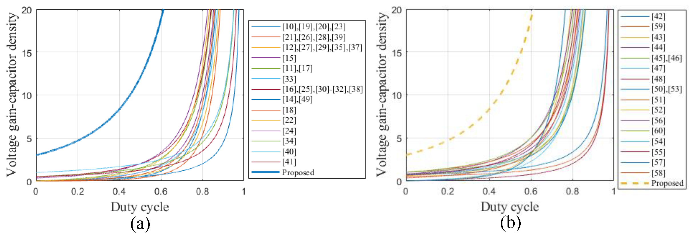
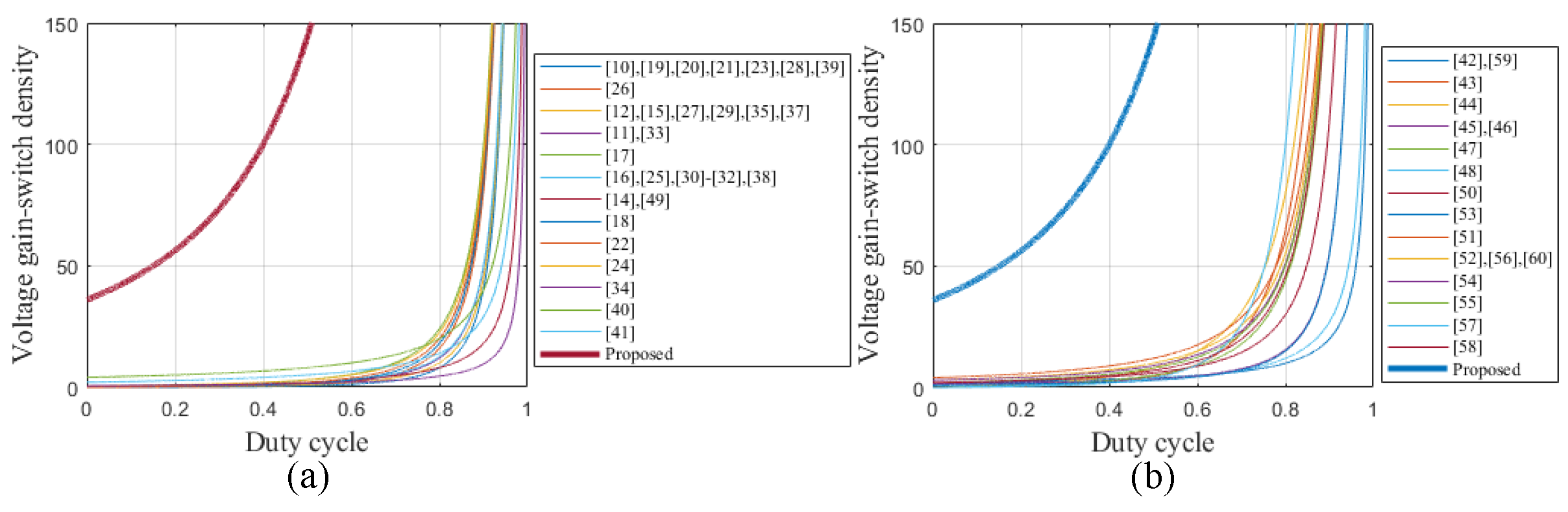
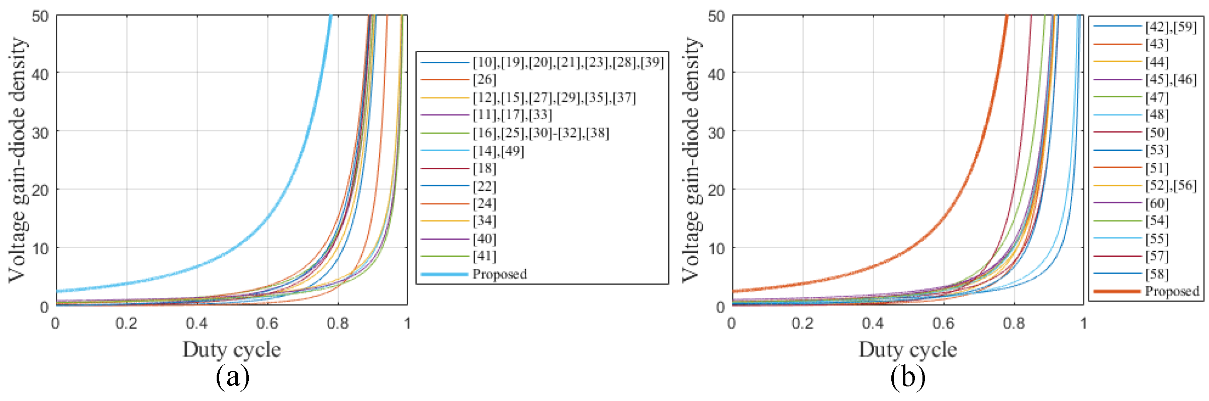
4. Voltage Gain and Voltage Gain Density Comparison of the Proposed Topology with Other High-Gain Topologies

One of the prominent points of the proposed topology is its voltage gain. Figure 10 compares the voltage gains. According to this figure, the proposed topology’s provided voltage gain is higher than that of [10,11,12,13,14,15,16,17,18,19,20,21,22,23,24,25,26,27,28,29,30,31,32,33,34,35,36,37,38,39,40,41,42,43,44,45,46,47,48,49,50,51,52,53,54,55,56,57,58,59,60]. Notably, the proposed topology’s provided voltage gain at low-duty cycles is higher than that of [10,11,12,13,14,15,16,17,18,19,20,21,22,23,24,25,26,27,28,29,30,31,32,33,34,35,36,37,38,39,40,41,42,43,44,45,46,47,48,49,50,51,52,53,54,55,56,57,58,59,60]. At higher-duty cycles. In comparing different components, let us consider the number of inductors, capacitors, switches, diodes, and overall components. Table 1 and Table 2 showcase these numbers. The proposed topology has more capacitors, diodes, and overall components than the other topologies. In terms of switch number, the proposed and most other converters have the same number of switches. However, the lower component count results in a lower voltage gain, which is consistent with references [10,11,12,13,14,15,16,17,18,19,20,21,22,23,24,25,26,27,28,29,30,31,32,33,34,35,36,37,38,39]. The design of the proposed topology is further analyzed by discussing the voltage gain density over the number of components. Figure 11 illustrates the voltage gain density over the components at all duty cycles. It shows that the proposed topology has a higher gain density. Additionally, Figure 12, Figure 13, Figure 14 and Figure 15 present the voltage gain density over each type of component. According to these figures, the proposed topology has the highest voltage gain density in terms of inductors, capacitors, switches, and diodes. These results highlight that the superior voltage gain is not solely due to the number of components but also signifies a better design compared to other topologies. To better understand the superiority of the proposed topology in terms of voltage gain density, the value of this parameter is extracted per type of component number. The voltage gain of converters is calculated at a 50% duty cycle, where the energy-storing and -releasing times are the same. Table 3 displays the voltage gain density over the number of inductors, capacitors, switches, diodes, and overall components. It becomes evident that the proposed topology has the highest voltage gain density, justifying the number of components employed in it.

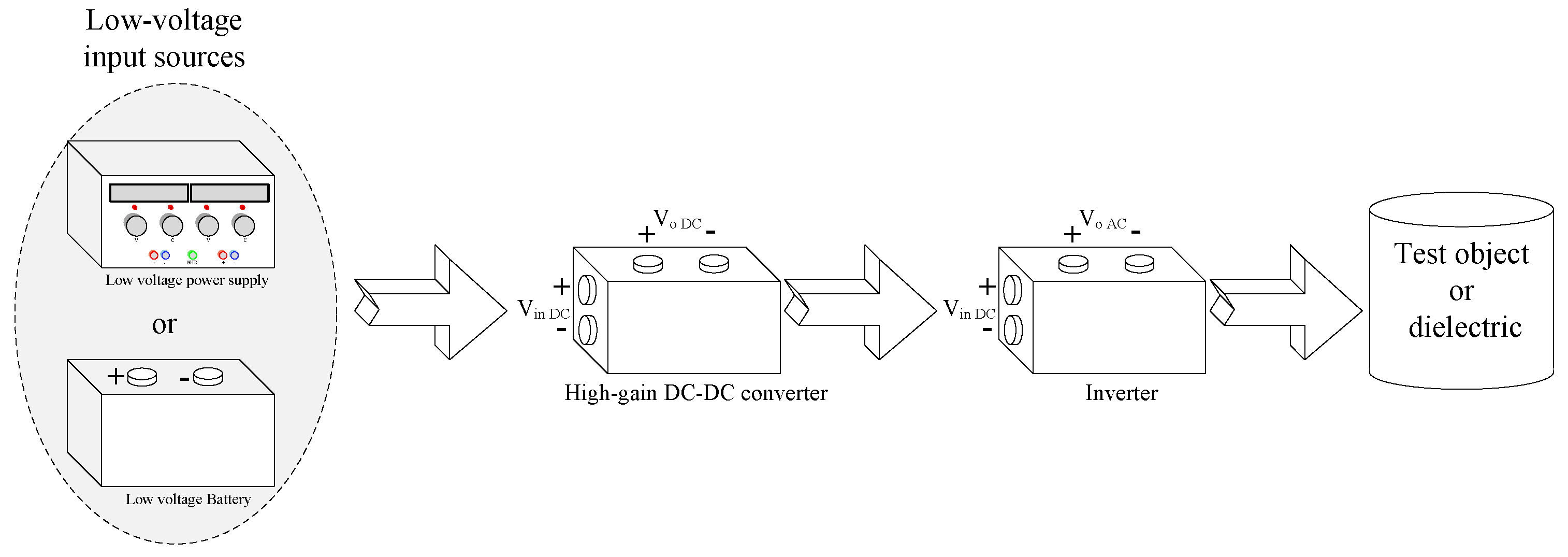
5. Application of the Proposed Topology

High-step-up DC–DC converters are used in various applications, as shown in Figure 16. A number of dielectric test procedures require a high DC voltage. Using a non-isolated high-gain DC–DC converter to supply this voltage reduces the size and weight of the testing equipment. One common application of this setup is measuring the dielectric resistance of equipment, which necessitates both a high DC voltage and a pico ammeter. Additionally, when the output voltage ripple is low enough, measuring a dielectric’s polarization and depolarization currents (PDC) becomes possible. This capability is valuable for monitoring the condition of high-voltage equipment. Another application of these converters is the electrolysis of water to produce hydrogen as a clean energy resource. The low DC voltage provided by renewable energy sources can be used as the input source of a high-gain DC–DC converter. The high voltage offered at the output of the DC–DC converter can be applied to a pulse power converter for the electrolysis of water to produce hydrogen.

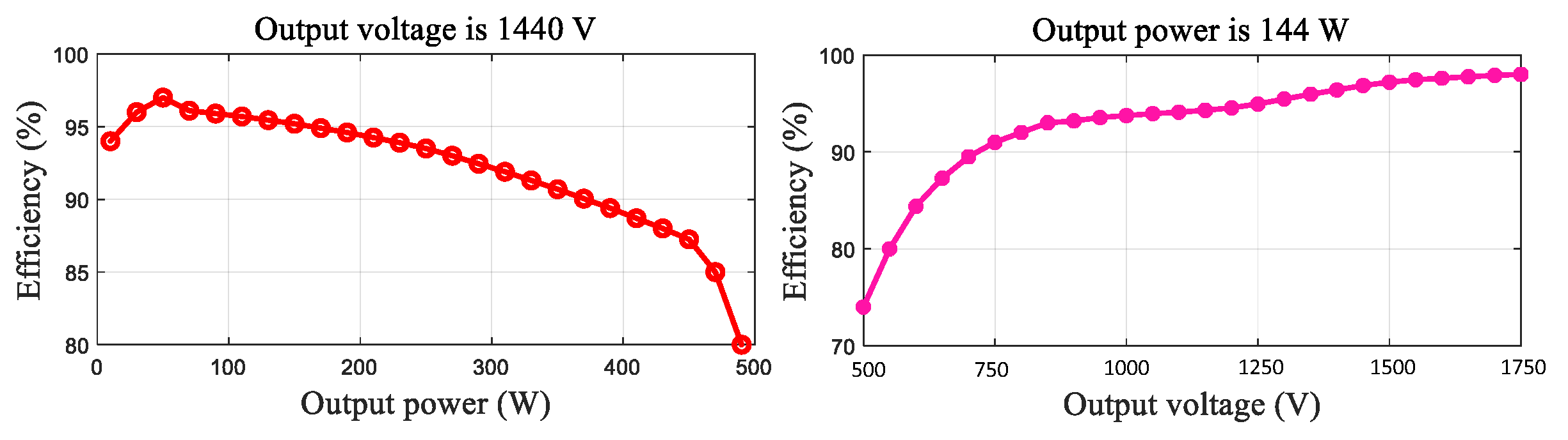
6. Experimental Results

The experimental results are discussed in this section to validate the extracted theoretical relations. The prototype of the converter is accessible by defining the voltage/current characteristics of the circuit components. In other words, the inductors’ average current, capacitors’ average voltage, and semiconductors’ voltage/current stresses must be determined. All these voltage variables are a function of the duty cycle, and input voltage and current variables are a function of the output current and duty cycle. Considering the safety considerations and measurement equipment limits, the input voltage, output current, and duty cycle are as follows:
V i n = 10 V I o = 55 mA D = 50 %
The input voltage and output current have been considered according to safety considerations, components, and measurement equipment limits. The mentioned duty cycle leads to equal energy storage and release times. According to the expressed values and reported relations in the second section, the inductors’ average current, capacitors’ average voltage, and semiconductors’ voltage/current stresses are as follows:
I L 1 = I L 2 = 18 ( 1 D ) 2 I o = 4 A I L 3 = I L 4 = 3 1 D I o = 0.33 A
V C 1 = V i n = 10 V V C 2 = V C 3 = 2 1 D V i n = 40 V V C 4 = V C 5 = 2 1 D V i n = 40 V V C 6 = V C 7 = 6 1 D V i n = 120 V V C 8 = V C 9 = 12 ( 1 D ) 2 V i n = 480 V V C 10 = V C 11 = 12 ( 1 D ) 2 V i n = 480 V V o = 6 1 D 2 V i n = 1440 V
I S = 35 + 2 D D 2 ( 1 D ) 2 I o = 7.9 A I D 1 = I D 2 = 18 ( 1 D ) 2 I o = 4 A I D 3 = I D 4 = 6 1 D I o = 0.66 A I D 5 = I D 6 = I D 7 = 6 1 D I o = 0.66 A I D 8 = I D 9 = 3 1 D I o = 0.33 A I D 10 = 5 + D 1 D I o = 0.61 A I D 11 = I D 12 = I D 13 = I o = 0.055 A I D 14 = I D 15 = I o = 0.055 A
V D 1 = V D 2 = V i n 1 D = 20 V V D 3 = V D 4 = 2 1 D V i n = 40 V V D 5 = V D 6 = V D 7 = 2 1 D V i n = 40 V V D 8 = V D 9 = 6 ( 1 D ) 2 V i n = 240 V V S = V D 11 = 12 ( 1 D ) 2 V i n = 480 V V D 12 = V D 13 = 12 ( 1 D ) 2 V i n = 480 V V D 14 = V D 15 = 12 ( 1 D ) 2 V i n = 480 V
To determine the inductors’ and capacitors’ values, the inductors’ current ripple, capacitors’ voltage ripple, and switching frequency are as follows:
Δ i L = 30 % Δ v c = 5 % f s = 50 kHz
According to the power quality standards, the voltage ripple must be between 1% and 10%, and the current ripple must be between 20% and 40%. In this study, the average value of the lower and upper margins was used. According to the mentioned values, the inductors’ and capacitors’ values are as follows:
Δ i L 1 = D V i n L 1 f s 83 μ H Δ i L 2 = D V i n L 2 f s 83 μ H Δ i L 3 = 6 D V i n ( 1 D ) L 3 f s 12 mH Δ i L 4 = 6 D V i n ( 1 D ) L 4 f s 12 mH
Δ V C 1 = 18 I o ( 1 D ) C 1 f s 80 μ F Δ V C 2 = 6 I o ( 1 D ) C 2 f s 6.6 μ F Δ V C 3 = 12 I o ( 1 D ) C 3 f s 13 μ F Δ V C 4 = 6 I o ( 1 D ) C 4 f s 6.6 μ F Δ V C 5 = 6 I o ( 1 D ) C 5 f s 6.6 μ F Δ V C 6 = 3 ( 3 + D ) I o ( 1 D ) C 6 f s 3.8 μ F Δ V C 7 = 3 I o C 7 f s 550 nF Δ V C 8 = I o C 8 f s 46 nF Δ V C 9 = 2 I o C 9 f s 96 nF Δ V C 10 = I o C 10 f s 46 nF Δ V C 11 = I o C 11 f s 96 nF Δ V o = ( 1 + D ) I o C o f s 69 nF
The calculated values are minimum values, and higher values for capacitors can be used spatially. According to the expressed values, the component types are reported in Table 4. According to the mentioned types, the prototype is presented in Figure 17. Additionally, the experimental results are presented in Figure 18. In this figure, the current waveforms of the inductors, the voltage waveforms of the capacitors, and voltage/current waveforms of the semiconductors are the extracted experimental results.
According to the experimental results in Figure 18, the inductors’ average current, capacitors’ average voltage, semiconductors’ average current, and semiconductors’ peak voltage are as follows:
I L 1 = 3.7 A I L 2 = 3.7 A I L 3 = 0.31 A I L 4 = 0.31 A
V C 1 = 9.7 V V C 2 = 39.5 V V C 3 = 38.7 V V C 4 = 36.5 V V C 5 = 36.5 V V C 6 = 112.2 V V C 7 = 112 V V C 8 = 450 V V C 9 = 450 V V C 10 = 448.5 V V C 11 = 448.4 V V o = 1360 V
I S = 7.1 A I D 1 = I D 2 = 3.7 A I D 3 = I D 4 = 0.62 A I D 5 = I D 6 = I D 7 = 0.62 A I D 8 = I D 9 = 0.3 A I D 10 = 0.59 A I D 11 = I D 12 = I D 13 = 0.051 A I D 14 = I D 15 = 0.051 A
V D 1 = V D 2 = 19 V V D 3 = V D 4 = 38 V V D 5 = V D 6 = 38 V V D 8 = V D 9 = 225 V V S = V D 11 = 450 V V D 12 = V D 13 = 450 V V D 14 = V D 15 = 450 V
It can be understood that the extracted values are compatible with the design considerations, and the differences are in the parasitic components of the circuit elements. The efficiency of the converter according to the extracted data is illustrated in Figure 19 as a pie chart. It is worth noting that the mentioned application for the proposed topology does not need high-efficiency values. Additionally, the current values are less than the considered value in the experimental results. Consequently, the conduction losses are not a dramatic issue in this study. Notably, the efficiency of the proposed converter is extracted for a varying output voltage and constant output power besides a constant output voltage and varying output power. Both conditions show an acceptable value of efficiency in Figure 20. To provide higher output voltages, two proposed topologies can be used in a stacked form, as in Figure 21. In this condition, the input sources must be isolated from each other, and the switch of the second converter must be derived as a high-sided switch. The extracted output voltages are presented in Figure 22. According to this figure, a 2680 V is provided with such a structure. Consequently, a much higher value than this, which is used in very-high-voltage DC tests of dielectrics, can be achieved by increasing the number of stacked levels.

7. Conclusions

An ultra-high step-up DC–DC converter is proposed. A high voltage gain was provided without a high-frequency transformer and a high-duty cycle. Moreover, the semiconductors’ voltage stress was less than the output voltage. A high voltage gain density was also extracted from the proposed topology, which justified the number of components and the voltage gain value. Such a high voltage density was extracted according to all types of components. The current stress of the semiconductors was low and acceptable, making the design of such a converter easier. Furthermore, the provided voltage gain by the proposed topology is high enough that the stacked connection of two converters from this type can easily achieve a 2.6 kV without using transformers. All these points make the proposed topology suitable for dielectric test applications.

Author Contributions

H.G.: Conceptualization, Data curation, Formal analysis, Investigation, Methodology, Resources, Software, Writing—original draft; R.S.S.: Formal analysis, Investigation, Software, Validation; S.A.: Investigation, Software, Validation; T.R.: Data curation, Project administration, Supervision, Writing—review & editing. All authors have read and agreed to the published version of the manuscript.

Funding

This research received no external funding.

Data Availability Statement

The data presented in this study are available on request from the corresponding author.

Conflicts of Interest

The authors declare no conflicts of interest.

References

  1. Mohammadi, F.; Gharehpetian, G.B.; Rastegar, H.; Farhadi-Kangarlu, M. Non-isolated Step-up DC-DC Converter Based on Switched Capacitor Cells. CSEE J. Power Energy Syst. 2023, 9, 1161–1172. [Google Scholar] [CrossRef]
  2. Forouzesh, M.; Siwakoti, Y.P.; Gorji, S.A.; Blaabjerg, F.; Lehman, B. Step-Up DC–DC Converters: A Comprehensive Review of Voltage-Boosting Techniques, Topologies, and Applications. IEEE Trans. Power Electron. 2017, 32, 9143–9178. [Google Scholar] [CrossRef]
  3. Hakemibarabadi, A.; Gorji, S.A.; Sera, D.; Walker, G. DZ-Source Converter: A Duality Inspiration of Z-Source Converter for Current-Source High-Conversion Ratio Applications. In Proceedings of the 2022 IEEE Energy Conversion Congress and Exposition (ECCE), Detroit, MI, USA, 9–13 October 2022; pp. 1–4. [Google Scholar] [CrossRef]
  4. Imanlou, A.; Seifi Najmi, E.; Babaei, E. A new high voltage gain DC-DC converter based on active switched-inductor technique. Int. J. Circuit Theory Appl. 2024, 52, 634–657. [Google Scholar] [CrossRef]
  5. Hasanpour, S.; Nouri, T.; Shaneh, M. Analysis and Design of a New Ultra-Step-Up DC–DC Converter with Reduced Voltage Stress for Renewable Energy Systems Applications. Iran J. Sci. Technol. Trans. Electr. Eng. 2023, 48, 817–830. [Google Scholar] [CrossRef]
  6. Hasanpour, S.; Lee, S.S. New Step-Up DC/DC Converter with Ripple-Free Input Current. IEEE Trans. Power Electron. 2024, 39, 2811–2821. [Google Scholar] [CrossRef]
  7. Hasanpour, S.; Lee, S.S. A New Quadratic DC/DC Converter with Ultra-High Voltage Gain. IEEE Trans. Power Electron. 2024, 39, 8800–8812. [Google Scholar] [CrossRef]
  8. Sun, D.; Ge, B.; Yan, X.; Bi, D.; Zhang, H.; Liu, Y.; Abu-Rub, H.; Ben-Brahim, L.; Peng, F.Z. Modeling, Impedance Design, and Efficiency Analysis of Quasi- Z Source Module in Cascaded Multilevel Photovoltaic Power System. IEEE Trans. Ind. Electron. 2014, 61, 6108–6117. [Google Scholar] [CrossRef]
  9. Mizani, A.; Shoushtari, M.; Shoulaie, A. A Novel Quadratic High Step-up DC-DC converter. In Proceedings of the 2020 11th Power Electronics, Drive Systems, and Technologies Conference (PEDSTC), Tehran, Iran, 4–6 February 2020; pp. 1–6. [Google Scholar] [CrossRef]
  10. Miao, S.; Wang, F.; Ma, X. A New Transformerless Buck–Boost Converter with Positive Output Voltage. IEEE Trans. Ind. Electron. 2016, 63, 2965–2975. [Google Scholar] [CrossRef]
  11. Ding, S.; Wang, F. A New Negative Output Buck–Boost Converter with Wide Conversion Ratio. IEEE Trans. Ind. Electron. 2017, 64, 9322–9333. [Google Scholar] [CrossRef]
  12. Maroti, P.K.; Padmanaban, S.; Wheeler, P.; Blaabjerg, F.; Rivera, M. Modified high voltage conversion inverting cuk DC-DC converter for renewable energy application. In Proceedings of the 2017 IEEE Southern Power Electronics Conference (SPEC), Puerto Varas, Chile, 4–7 December 2017; pp. 1–5. [Google Scholar] [CrossRef]
  13. Valdez-Resendiz, J.E.; Rosas-Caro, J.C.; Mayo-Maldonado, J.C.; Llamas-Terres, A. Quadratic boost converter based on stackable switching stages. IET Power Electron. 2018, 11, 1373–1381. [Google Scholar] [CrossRef]
  14. Ahmadi, M.; Hosseinpour, M.; Mousavi-Aghdam, S.R.; Sedaghati, F. A High Conversion Ratio Transformerless Buck-Boost Converter with Continuous Input Current. In Proceedings of the 2021 12th Power Electronics, Drive Systems, and Technologies Conference (PEDSTC), Tabriz, Iran, 2–4 February 2021; pp. 1–7. [Google Scholar] [CrossRef]
  15. García-Vite, P.M.; Soriano-Rangel, C.A.; Rosas-Caro, J.C.; Mancilla–David, F. A DC–DC converter with quadratic gain and input current ripple cancelation at a selectable duty cycle. Renew. Energy 2017, 101, 431–436. [Google Scholar] [CrossRef]
  16. Wang, F. A novel quadratic Boost converter with low current and voltage stress on power switch for fuel-cell system applications. Renew. Energy 2018, 115, 836–845. [Google Scholar] [CrossRef]
  17. Mostaan, A.; Gorji, S.A.; Soltani, M.N.; Ektesabi, M. A novel single switch transformerless quadratic DC/DC buck-boost converter. In Proceedings of the 2017 19th European Conference on Power Electronics and Applications (EPE’17 ECCE Europe), Warsaw, Poland, 11–14 September 2017; pp. 1–6. [Google Scholar] [CrossRef]
  18. Allahverdinejad, B.; Modaberi, S.A.; Ajami, A. A Non-isolated Buck-Boost DC–DC Converter with Continuous Input Current and Wide Conversion Ratio Range for Photovoltaic Applications. In Proceedings of the 2022 13th Power Electronics, Drive Systems, and Technologies Conference (PEDSTC), Tehran, Iran, 1–3 February 2022; pp. 491–497. [Google Scholar] [CrossRef]
  19. Rosas-Caro, J.C.; Sanchez, V.M.; Valdez-Resendiz, J.E.; Mayo-Maldonado, J.C.; Beltran-Carbajal, F.; Valderrabano-Gonzalez, A. Quadratic buck-boost converter with positive output-voltage and continuous input-current. In Proceedings of the 2018 International Conference on Electronics, Communications and Computers (CONIELECOMP), Cholula, Mexico, 21–23 February 2018; pp. 152–158. [Google Scholar] [CrossRef]
  20. Rosas-Caro, J.C.; Valdez-Resendiz, J.E.; Mayo-Maldonado, J.C.; Alejo-Reyes, A.; Valderrabano-Gonzalez, A. Quadratic buck–boost converter with positive output voltage and minimum ripple point design. IET Power Electron. 2018, 11, 1306–1313. [Google Scholar] [CrossRef]
  21. Sarikhani, A.; Allahverdinejad, B.; Hamzeh, M.; Afjei, E. A continuous input and output current quadratic buck-boost converter with positive output voltage for photovoltaic applications. Sol. Energy 2019, 188, 19–27. [Google Scholar] [CrossRef]
  22. Sarikhani, A.; Allahverdinejad, B.; Hamzeh, M. A Nonisolated Buck–Boost DC–DC Converter with Continuous Input Current for Photovoltaic Applications. IEEE J. Emerg. Sel. Top. Power Electron. 2021, 9, 804–811. [Google Scholar] [CrossRef]
  23. Loera-Palomo, R.; Morales-Saldaña, J.A.; Rivero, M.; Álvarez-Macías, C.; Hernández-Jacobo, C.A. Noncascading Quadratic Buck-Boost Converter for Photovoltaic Applications. Micromachines 2021, 12, 984. [Google Scholar] [CrossRef] [PubMed]
  24. Naresh, S.V.K.; Peddapati, S.; Alghaythi, M.L. Non-Isolated High Gain Quadratic Boost Converter Based on Inductor’s Asymmetric Input Voltage. IEEE Access 2021, 9, 162108–162121. [Google Scholar] [CrossRef]
  25. Gupta, N.; Bhaskar, M.S.; Almakhles, D.; Sanjeevikumar, P.; Blaabjerg, F.; Leonowicz, Z. Two-Tier Converter: A New Structure of High Gain DC-DC Converter with Reduced Voltage Stress. In Proceedings of the 2020 IEEE International Conference on Environment and Electrical Engineering and 2020 IEEE Industrial and Commercial Power Systems Europe (EEEIC/I&CPS Europe), Madrid, Spain, 9–12 June 2020; pp. 1–6. [Google Scholar] [CrossRef]
  26. Zhang, N.; Zhang, G.; See, K.W.; Zhang, B. A Single-Switch Quadratic Buck–Boost Converter with Continuous Input Port Current and Continuous Output Port Current. IEEE Trans. Power Electron. 2018, 33, 4157–4166. [Google Scholar] [CrossRef]
  27. Maroti, P.K.; Padmanaban, S.; Holm-Nielsen, J.B.; Bhaskar, M.S.; Meraj, M.; Iqbal, A. A New Structure of High Voltage Gain SEPIC Converter for Renewable Energy Applications. IEEE Access 2019, 7, 89857–89868. [Google Scholar] [CrossRef]
  28. Gholizadeh, H.; Salehi, M.; Rafiee, Z.; Afjei, E.; Hamzeh, M. A Transformer less Quadratic Buck-Boost Converter with Wide Range of Output Voltage and Low Switch Stresses. In Proceedings of the 2020 11th Power Electronics, Drive Systems, and Technologies Conference (PEDSTC), Tehran, Iran, 4–6 February 2020; pp. 1–6. [Google Scholar] [CrossRef]
  29. Gholizadeh, H.; Aboufazeli, S.; Rafiee, Z.; Afjei, E.; Hamzeh, M. A Non-Isolated High Gain DC-DC Converters with Positive Output Voltage and Reduced Current Stresses. In Proceedings of the 2020 11th Power Electronics, Drive Systems, and Technologies Conference (PEDSTC), Tehran, Iran, 4–6 February 2020; pp. 1–6. [Google Scholar] [CrossRef]
  30. Golizedeh, H.; Hashemi, M.R.; Rafiee, Z.; Hamzeh, M.; Afjei, E. A Quadratic Boost Converter with Continuous Input Current and Suitable for Photo Voltaic Solar Panels. In Proceedings of the 2020 28th Iranian Conference on Electrical Engineering (ICEE), Tabriz, Iran, 4–6 August 2020; pp. 1–5. [Google Scholar] [CrossRef]
  31. Afjei, E.; Siadatan, A.; Rezaei-Zare, A.; Gholizadeh, H. A Quadratic Boost Converter with Continuous Input Current and Low Normalized Voltage/Current Stresses. In Proceedings of the 2022 International Symposium on Power Electronics, Electrical Drives, Automation and Motion (SPEEDAM), Sorrento, Italy, 22–24 June 2022; pp. 395–401. [Google Scholar] [CrossRef]
  32. Sharifi Shahrivar, R.; Gholizadeh, H.; Siadatan, A.; Afjei, S.E. Design and Implementation of a Modified Boost Topology with High Voltage Ratio and Efficiency Besides the Lower Semiconductors Stresses. Res. Technol. Electr. Ind. 2022, 1, 75–84. [Google Scholar] [CrossRef]
  33. Gholizadeh, H.; Gorji, S.A.; Afjei, E.; Sera, D. Design and Implementation of a New Cuk-Based Step-Up DC–DC Converter. Energies 2021, 14, 6975. [Google Scholar] [CrossRef]
  34. Rahimi, T.; Islam, M.R.; Gholizadeh, H.; Mahdizadeh, S.; Afjei, E. Design and Implementation of a High Step-Up DC-DC Converter Based on the Conventional Boost and Buck-Boost Converters with High Value of the Efficiency Suitable for Renewable Application. Sustainability 2021, 13, 10699. [Google Scholar] [CrossRef]
  35. Totonchi, N.; Gholizadeh, H.; Afjei, E.; Hamzeh, M. A Novel Transformer less High Gain DC-DC Converter with Continuous Input Current and Suitable for Photo Voltaic Panels. In Proceedings of the 2020 11th Power Electronics, Drive Systems, and Technologies Conference (PEDSTC), Tehran, Iran, 4–6 February 2020; pp. 1–6. [Google Scholar] [CrossRef]
  36. Marzoni, A.T.; Amini, S.; Gholizadeh, H.; Kalamialhashem, S.M.; Afjei, E. A Quadratic DC-DC converter with Continuous Input Current And Selectable Duty Cycle to Provide A Zero Current Switching of Switch Suitable for renewable Applications. In Proceedings of the 2022 9th Iranian Conference on Renewable Energy and Distributed Generation (ICREDG), Mashhad, Iran, 23–24 February 2022; pp. 1–5. [Google Scholar] [CrossRef]
  37. Monfared, M.T.; Gholizadeh, H.; Amini, S.; Kalamialhashem, S.M.; Afjei, S.A.A.; Afjei, S.E. A Modified Zeta DC-DC Converter with Higher Voltage Gain Besides Low Value of the Normalized Current Stresses. In Proceedings of the 2022 13th Power Electronics, Drive Systems, and Technologies Conference (PEDSTC), Tehran, Iran, 1–3 February 2022; pp. 269–274. [Google Scholar] [CrossRef]
  38. Monfared, M.T.; Gholizadeh, H.; Ben-Brahim, L. New Enhanced Family of QBC Topologies: Mitigating Capacitor Stress and Increasing Voltage Gain. In Proceedings of the 2024 IEEE 8th Energy Conference (ENERGYCON), Doha, Qatar, 4–7 March 2024; pp. 1–6. [Google Scholar] [CrossRef]
  39. Gholizadeh, H.; Gorji, S.A.; Sera, D. A Quadratic Buck-Boost Converter with Continuous Input and Output Currents. IEEE Access 2023, 11, 22376–22393. [Google Scholar] [CrossRef]
  40. Banaei, M.R.; Ajdar Faeghi Bonab, H. High-efficiency transformerless buck–boost DC–DC converter. Int. J. Circuit Theory Appl. 2017, 45, 1129–1150. [Google Scholar] [CrossRef]
  41. Shokri, G.; Naderi, E.; SeyedShenava, S. Active and Reactive Power Control of Grid-Connected PV Power Systems based on HGNISS DC-DC Converter and SMDPC Strategy. In Proceedings of the 2020 11th Power Electronics, Drive Systems, and Technologies Conference (PEDSTC), Tehran, Iran, 4–6 February 2020; pp. 1–6. [Google Scholar] [CrossRef]
  42. Ghabeli Sani, S.; Mohammadi, F.; Banaei, M.R.; Farhadi-Kangarlu, M. Design and implementation of a new high step-up DC-DC converter for renewable applications. Int. J. Circuit Theory Appl. 2019, 47, 464–482. [Google Scholar] [CrossRef]
  43. Amir, A.; Che, H.S.; Amir, A.; Khateb, A.E.; Rahim, N.A. Transformerless high gain boost and buck-boost DC-DC converters based on extendable switched capacitor (SC) cell for stand-alone photovoltaic system. Sol. Energy 2018, 171, 212–222. [Google Scholar] [CrossRef]
  44. Sanjeevikumar, P.; Maroti, P.K.; Blaabjerg, F.; Holm-Nielsen, J.B.; Ionel, D.M.; He, J. Modified CUK Converter with Two Switched Inductor Module Configurations for Photovoltaic Application: Part-II. In Proceedings of the 2020 IEEE International Conference on Environment and Electrical Engineering and 2020 IEEE Industrial and Commercial Power Systems Europe (EEEIC / I&CPS Europe), Madrid, Spain, 9–12 June 2020; pp. 1–6. [Google Scholar] [CrossRef]
  45. Maroti, P.K.; Al-Ammari, R.; Iqbal, A.; Ben-Brahim, L.; Padmanaban, S.; Abu-Rub, H. A Novel High Gain Configurations of Modified SEPIC Converter for Renewable Energy Applications. In Proceedings of the 2019 IEEE 28th International Symposium on Industrial Electronics (ISIE), Vancouver, BC, Canada, 12–14 June 2019; pp. 2503–2508. [Google Scholar] [CrossRef]
  46. Lee, S.S.; Chu, B.; Lim, C.S.; Lee, K.B. Two-Inductor Non-Isolated DC-DC Converter with High Step-Up Voltage Gain. J. Power Electron. 2019, 19, 1069–1073. [Google Scholar] [CrossRef]
  47. Varesi, K.; Hassanpour, N.; Saeidabadi, S. Novel high step-up DC–DC converter with increased voltage gain per devices and continuous input current suitable for DC microgrid applications. Int. J. Circuit Theory Appl. 2020, 48, 1820–1837. [Google Scholar] [CrossRef]
  48. Hosseinpour, M.; Ahmadi, M.; Seifi, A.; Mousavi-Aghdam, S.R. A new transformerless semi-quadratic buck–boost converter based on combination of Cuk and traditional buck–boost converters. Int. J. Circuit Theory Appl. 2022, 50, 3926–3948. [Google Scholar] [CrossRef]
  49. Banaei, M.R.; Sani, S.G. Analysis and Implementation of a New SEPIC-Based Single-Switch Buck–Boost DC–DC Converter with Continuous Input Current. IEEE Trans. Power Electron. 2018, 33, 10317–10325. [Google Scholar] [CrossRef]
  50. Gholizadeh, H.; Sharifi Shahrivar, R.; Hashemi, M.R.; Afjei, E.; A. Gorji, S. Design and Implementation a Single-Switch Step-Up DC-DC Converter Based on Cascaded Boost and Luo Converters. Energies 2021, 14, 3584. [Google Scholar] [CrossRef]
  51. Mahdizadeh, S.; Gholizadeh, H.; Shahrivar, R.; Afjei, E.; Mosallanejad, A. An ultra high step-up DC-DC converter based on VMC, POSLLC, and boost converter. IET Power Electron. 2022, 15, 901–918. [Google Scholar] [CrossRef]
  52. Rahimi, T.; Ding, L.; Gholizadeh, H.; Shahrivar, R.S.; Faraji, R. An Ultra High Step-Up DC–DC Converter Based on the Boost, Luo, and Voltage Doubler Structure: Mathematical Expression, Simulation, and Experimental. IEEE Access 2021, 9, 132011–132024. [Google Scholar] [CrossRef]
  53. Mahdizadeh, S.; Gholizadeh, H.; Gorji, S.A. A Power Converter Based on the Combination of Cuk and Positive Output Super Lift Lou Converters: Circuit Analysis, Simulation and Experimental Validation. IEEE Access 2022, 10, 52899–52911. [Google Scholar] [CrossRef]
  54. Totonchi, N.; Gholizadeh, H.; Mahdizadeh, S.; Afjei, E. A High Step up DC-DC Converter Based on the Cascade Boost, Voltage Multiplier Cell and Self Lift Luo Converter. In Proceedings of the 2020 10th Smart Grid Conference (SGC), Kashan, Iran, 16–17 December 2020; pp. 1–5. [Google Scholar] [CrossRef]
  55. Totonchi, N.; Gholizadeh, H.; Afjei, E. A Transformer-less Double Quadratic Boost Converter with Positive Output Polarity and Non Zero Input Current. In Proceedings of the 2020 28th Iranian Conference on Electrical Engineering (ICEE), Tabriz, Iran, 4–6 August 2020; pp. 1–5. [Google Scholar] [CrossRef]
  56. Gholizadeh, H.; Ben-Brahim, L. A New Non-Isolated High-Gain Single-Switch DC-DC Converter Topology with a Continuous Input Current. Electronics 2022, 11, 2900. [Google Scholar] [CrossRef]
  57. Monfared, M.T.; Gholizadeh, H.; Kalamialhashem, S.M.; Amini, S.; Afjei, S.A.A.; Afjei, S.E. A Cubic Transformer-less DC-DC Converter with Continuous Input Current: Mathematical model, Simulation, and Experimental. In Proceedings of the 2022 13th Power Electronics, Drive Systems, and Technologies Conference (PEDSTC), Tehran, Iran, 1–3 February 2022; pp. 19–25. [Google Scholar] [CrossRef]
  58. Gholizadeh, H.; Ben-Brahim, L. A High-Gain Single-Switch DC-DC Converter Based on Cascaded Boost and Voltage Lift Technique. In Proceedings of the 2024 IEEE 8th Energy Conference (ENERGYCON), Doha, Qatar, 4–7 March 2024; pp. 1–6. [Google Scholar] [CrossRef]
  59. Gorji, S.A.; Gholizadeh, H. A Modified Positive Output Super-Lift Luo DC-DC Converter with Improved Voltage Boost Ability. In Proceedings of the 2022 5th International Conference on Renewable Energy and Power Engineering (REPE), Beijing, China, 28–30 September 2022; pp. 282–286. [Google Scholar] [CrossRef]
  60. Gorji, S.A.; Gholizadeh, H.; Sera, D. A New Non-Isolated High-Gain Single-Switch DC-DC Converter with Continuous Input Current. In Proceedings of the IECON 2023- 49th Annual Conference of the IEEE Industrial Electronics Society, Singapore, 16–19 October 2023; pp. 1–5. [Google Scholar] [CrossRef]
  61. Alkhaldi, A.; Elkhateb, A.; Laverty, D. Voltage Lifting Techniques for Non-Isolated DC/DC Converters. Electronics 2023, 12, 718. [Google Scholar] [CrossRef]
  62. Jalilyan, S.; Abbasi, V.; Varmenjeh, A.R.; Ahmadian, S.; Gorji, S.A. High Voltage-Gain Common-Ground Three-Port DC-DC Converter with Low Current Ripples on the PV Source for Standalone Applications. IEEE Access 2024, 12, 80896–80909. [Google Scholar] [CrossRef]
  63. Gorji, S.A.; Sahebi, H.G.; Movahed, M.; Ektesabi, M. Multi-Input Boost DC-DC Converter with Continuous Input-Output Current for Renewable Energy Systems. In Proceedings of the 2019 IEEE 4th International Future Energy Electronics Conference (IFEEC), Singapore, 25–28 November 2019; pp. 1–5. [Google Scholar] [CrossRef]
  64. Shaabani, M.; Mirzaei, A.; Rezvanyvardom, M.; Khosravi, F.; Gorji, S.A. A Hybrid Switched-Inductor/Switched-Capacitor DC-DC Converter with High Voltage Gain Using a Single Switch for Photovoltaic Application. Energies 2023, 16, 5524. [Google Scholar] [CrossRef]
  65. Taghavi, S.S.; Rezvanyvardom, M.; Mirzaei, A.; A. Gorji, S. High Step-Up Three-Level Soft Switching DC-DC Converter for Photovoltaic Generation Systems. Energies 2023, 16, 41. [Google Scholar] [CrossRef]
  66. Mahdizadeh, A.H.; Kashani, M.; Soltani, M.; Hajizadeh, A.; Gorji, S.A. A Quadratic Boost Converter Suitable for Fuel Cell-Powered Electric Vehicles. In Proceedings of the IECON 2023- 49th Annual Conference of the IEEE Industrial Electronics Society, Singapore, 16–19 October 2023; pp. 1–6. [Google Scholar] [CrossRef]
  67. Alilou, S.M.; Ahmadi, S.; Maalandish, M.; Hosseini, S.H. A Transformerless Single-Switch DC-DC Boost Converter Suitable for Renewable Energy Applications. In Proceedings of the 2022 30th International Conference on Electrical Engineering (ICEE), Tehran, Iran, 17–19 May 2022; pp. 221–226. [Google Scholar] [CrossRef]
  68. Azmoon-Asmarood, S.; Maalandish, M.; Shoghli, I.; Nazemi-Oskuee, S.H.R.; Hosseini, S.H. A non-isolated high step-up MIMO DC-DC converter for renewable energy applications. IET Power Electron. 2022, 15, 953–962. [Google Scholar] [CrossRef]
  69. Maalandish, M.; Hosseini, S.H.; Sabahi, M.; Rostami, N.; Khooban, M.-H. High step-up multi input–multi output DC–DC converter with high controllability for battery charger/EV applications. IET Power Electron. 2023, 16, 2606–2623. [Google Scholar] [CrossRef]
  70. Radmanesh, H.; Jashnani, H.; Pourjafar, S.; Maalandish, M. A dual-output single-input non-isolated DC-DC converter with reduced semiconductors stress. Int. J. Circuit Theory Appl. 2023, 51, 594–610. [Google Scholar] [CrossRef]
  71. Hassani, M.Y.; Maalandish, M.; Hosseini, S.H. A New Single-Input Multioutput Interleaved High Step-Up DC–DC Converter for Sustainable Energy Applications. IEEE Trans. Power Electron. 2021, 36, 1544–1552. [Google Scholar] [CrossRef]
  72. Maalandish, M.; Hosseini, S.H.; Pourjafar, S.; Nouri, S.; Hashemzadeh, S.M.; Marangalu, M.G. A Non-isolated High Step-Up DC-DC Converter Recommended for Photovoltaic Systems. In Proceedings of the 2021 12th Power Electronics, Drive Systems, and Technologies Conference (PEDSTC), Tabriz, Iran, 2–4 February 2021; pp. 1–5. [Google Scholar] [CrossRef]
  73. Radmanesh, H.; Maalandish, M.; Pourjafar, S. A Non-Isolated High Step-up Two-Input Single Output DC-DC Converter with Less Number of Components. In Proceedings of the 2022 13th Power Electronics, Drive Systems, and Technologies Conference (PEDSTC), Tehran, Iran, 1–3 February 2022; pp. 574–579. [Google Scholar] [CrossRef]
  74. Radmanesh, H.; Jashnani, H.; Pourjafar, S.; Maalandish, M. Analyze and Implementation of High Gain DC-DC Topology Recommended for Renewable Power Generation. In Proceedings of the 2022 13th Power Electronics, Drive Systems, and Technologies Conference (PEDSTC), Tehran, Iran, 1–3 February 2022; pp. 294–299. [Google Scholar] [CrossRef]
  75. Hassani, M.Y.; Maalandish, M.; Hosseini, S.H. A Single-Switch High Step-Up DC–DC Converter with Low Input Current Ripple for Renewable Energy Applications. In Proceedings of the 2022 13th Power Electronics, Drive Systems, and Technologies Conference (PEDSTC), Tehran, Iran, 1–3 February 2022; pp. 186–190. [Google Scholar] [CrossRef]
  76. Shalbaf, A.A.; Shahidi, N.; Hemati, M. A high-gain interleaved DC-DC converter with reduced components for EV charging application. Comput. Electr. Eng. Part A 2024, 118, 109316. [Google Scholar] [CrossRef]
  77. Mollajafari, M.; Mohammadiazar, F.; Akbari, E.; Sheykhi, E.; Chaoui, H. A New Voltage-Multiplier-Based Power Converter Configuration Suitable for Renewable Energy Sources and Sustainability Applications. Sustainability 2022, 14, 16698. [Google Scholar] [CrossRef]
  78. Hayat, A.; Sibtain, D.; Murtaza, A.F.; Shahzad, S.; Jajja, M.S.; Kilic, H. Design and Analysis of Input Capacitor in DC–DC Boost Converter for Photovoltaic-Based Systems. Sustainability 2023, 15, 6321. [Google Scholar] [CrossRef]
  79. Alghaythi, M.L. A Non-Isolated High Voltage Gain DC–DC Converter Suitable for Sustainable Energy Systems. Sustainability 2023, 15, 12058. [Google Scholar] [CrossRef]
  80. Subbulakshmy, R.; Palanisamy, R.; Alshahrani, S.; Saleel, C.A. Implementation of Non-Isolated High Gain Interleaved DC-DC Converter for Fuel Cell Electric Vehicle Using ANN-Based MPPT Controller. Sustainability 2024, 16, 1335. [Google Scholar] [CrossRef]
  81. Almalaq, Y.; Matin, M. Three Topologies of a Non-Isolated High Gain Switched-Inductor Switched-Capacitor Step-Up Cuk Converter for Renewable Energy Applications. Electronics 2018, 7, 94. [Google Scholar] [CrossRef]
  82. Dimitrov, B.; Hayatleh, K.; Barker, S.; Collier, G.; Sharkh, S.; Cruden, A. A Buck-Boost Transformerless DC–DC Converter Based on IGBT Modules for Fast Charge of Electric Vehicles. Electronics 2020, 9, 397. [Google Scholar] [CrossRef]
  83. Huang, X.; Wang, H.; Zhou, Y.; Zhang, X.; Wang, Y.; Xu, H. Photovoltaic Power Plant Collection and Connection to HVDC Grid with High Voltage DC/DC Converter. Electronics 2021, 10, 3098. [Google Scholar] [CrossRef]
  84. Meshael, H.; Elkhateb, A.; Best, R. Topologies and Design Characteristics of Isolated High Step-Up DC–DC Converters for Photovoltaic Systems. Electronics 2023, 12, 3913. [Google Scholar] [CrossRef]
  85. Shahir, F.M.; Aberoumandazar, M.; Babaei, E. High Gain DC-DC Boost Converter Applied in Hybrid System of Photovoltaic and Battery. In Proceedings of the 2021 International Symposium on Devices, Circuits and Systems (ISDCS), Higashihiroshima, Japan, 3–5 March 2021; pp. 1–4. [Google Scholar] [CrossRef]
  86. Abolhassani, P.; Maalandish, M.; Nadermohammadi, A.; Sharifian, M.B.B.; Feyzi, M.R.; Hosseini, S.H. A high step-up high step-down coupled inductor based bidirectional DC–DC converter with low voltage stress on switches. IET Power Electron. 2024, 17, 802–823. [Google Scholar] [CrossRef]
  87. Maalandish, M.; Babaei, E.; Abolhasani, P.; Gheisarnejad, M.; Khooban, M.-H. Ultra high step-up soft-switching DC/DC converter using coupled inductor and interleaved technique. IET Power Electron. 2023, 16, 1320–1338. [Google Scholar] [CrossRef]
  88. Nadermohammadi, A.; Maalandish, M.; Seifi, A.; Abolhassani, P.; Hosseini, S.H.; Farsadi, M. A non-isolated single-switch ultra-high step-up DC–DC converter with coupled inductor and low-voltage stress on switch. IET Power Electron. 2024, 17, 251–265. [Google Scholar] [CrossRef]
  89. Pourjafar, S.; Sedaghati, F.; Shayeghi, H.; Maalandish, M. High step-up DC–DC converter with coupled inductor suitable for renewable applications. IET Power Electron. 2019, 12, 92–101. [Google Scholar] [CrossRef]
  90. Pourjafar, S.; Madadi Kojabadi, H.; Maalandish, M.; Abarzadeh, M.; Blaabjerg, F. Non-Isolated Coupled Inductor Based DC-DC Converter with High Voltage Conversion Ratio Recommended for Renewable Applications. Electr. Power Compon. Syst. 2021, 48, 1695–1707. [Google Scholar] [CrossRef]
  91. Pourjafar, S.; Shayeghi, H.; Hashemzadeh, S.M.; Sedaghati, F.; Maalandish, M. A non-isolated high step-up DC–DC converter using magnetic coupling and voltage multiplier circuit. IET Power Electron. 2021, 14, 1637–1655. [Google Scholar] [CrossRef]
  92. Sharma, P.; Hasanpour, S.; Kumar, R. A new soft-switching high step-up DC–DC converter with low voltage stress. Energy Sci. Eng. 2024, 12, 3062–3073. [Google Scholar] [CrossRef]
  93. Nouri, T.; Hasanpour, S.; Lee, S.S. A Semi-Quadratic Trans-Inverse High Step-Up DC-DC Converter for Renewable Energy Applications. IEEE Trans. Power Electron. 2024. [Google Scholar] [CrossRef]
  94. Hasanpour, S. A novel soft-switching quadratic high voltage gain trans-inverse DC/DC converter. IET Power Electron. 2024, 1–16. [Google Scholar] [CrossRef]
  95. Hasanpour, S.; Mostaan, A.; Haghighi, S.K.S. Dual-Output Classic Buck and Buck-Boost Converter with Fast Dynamic Response. IEEE J. Emerg. Sel. Top. Ind. Electron. 2024, 1–11. [Google Scholar] [CrossRef]
  96. Hasanpour, S.; Siwakoti, Y.P.; Blaabjerg, F. Analysis of a New Soft-Switched Step-Up Trans-Inverse DC/DC Converter Based on Three-Winding Coupled-Inductor. IEEE Trans. Power Electron. 2022, 37, 2203–2215. [Google Scholar] [CrossRef]
  97. Esmaeili, S.; Hasanpour, S.; Hafezi, H. New High Step-Up Coupled Dual Winding Quadratic Enhanced SEPIC DC-DC Converter. In Proceedings of the 2021 International Conference on Smart Energy Systems and Technologies (SEST), Vaasa, Finland, 6–8 September 2021; pp. 1–6. [Google Scholar] [CrossRef]
  98. Hasanpour, S.; Nouri, T.; Blaabjerg, F.; Siwakoti, Y.P. High Step-Up SEPIC-Based Trans-Inverse DC–DC Converter with Quasi-Resonance Operation for Renewable Energy Applications. IEEE Trans. Ind. Electron. 2023, 70, 485–497. [Google Scholar] [CrossRef]
  99. Hasanpour, S.; Siwakoti, Y.P.; Blaabjerg, F. A New High Efficiency High Step-Up DC/DC Converter for Renewable Energy Applications. IEEE Trans. Ind. Electron. 2023, 70, 1489–1500. [Google Scholar] [CrossRef]
  100. Hasanpour, S. New Structure of Single-Switch Ultra-High-Gain DC/DC Converter for Renewable Energy Applications. IEEE Trans. Power Electron. 2022, 37, 12715–12728. [Google Scholar] [CrossRef]
  101. Hasanpour, S.; Forouzesh, M.; Siwakoti, Y. Full Soft-Switching Ultra-High Gain DC/DC Converter Using Three-Winding Coupled-Inductor with Modular Scalability for Renewable Energy Applications. AUT J. Electr. Eng. 2022, 54, 49–66. [Google Scholar] [CrossRef]
  102. Upadhyay, P.; Sharma, P.; Khandelwal, S.; Kumar, R.; Hassanpour, S. An active clamp coupled inductor-based soft-switched quadratic boost converter. Int. J. Circuit Theory Appl. 2023, 51, 2141–2162. [Google Scholar] [CrossRef]
  103. Sharma, P.; Upadhyay, P.; Kumar, R.; Hassanpour, S. ZCS-ZVS Operation of a Double Frequency High-Voltage Gain Boost Converter. In Proceedings of the 2022 IEEE 19th India Council International Conference (INDICON), Kochi, India, 24–26 November 2022; pp. 1–6. [Google Scholar] [CrossRef]
  104. Esmaeili, S.; Shekari, M.; Rasouli, M.; Hasanpour, S.; Khan, A.A.; Hafezi, H. High Gain Magnetically Coupled Single Switch Quadratic Modified SEPIC DC-DC Converter. IEEE Trans. Ind. Appl. 2023, 59, 3593–3604. [Google Scholar] [CrossRef]
  105. Hasanpour, S.; Nouri, T. New Coupled-Inductor High-Gain DC/DC Converter with Bipolar Outputs. IEEE Trans. Ind. Electron. 2024, 71, 2601–2613. [Google Scholar] [CrossRef]
  106. Hasanpour, S.; Siwakoti, Y.P.; Blaabjerg, F. A New Soft-Switched High Step-Up Trans-Inverse DC/DC Converter Based on Built-In Transformer. IEEE Open J. Power Electron. 2023, 4, 381–394. [Google Scholar] [CrossRef]
  107. Mostaan, A.; Esmaeili, S.; Hasanpour, S.; Taleshani, T.B.; Khan, A.A. A Symmetric Bipolar Quadratic Buck–Boost Converter with Synchronous Triple Switches. IEEE J. Emerg. Sel. Top. Ind. Electron. 2023, 4, 1055–1062. [Google Scholar] [CrossRef]
  108. Hasanpour, S.; Siwakoti, Y.P.; Blaabjerg, F. A new soft-switching high gain DC/DC converter with bipolar outputs. IET Power Electron. 2024, 17, 144–156. [Google Scholar] [CrossRef]
  109. Wu, Y.-E.; Chiu, P.-N. A High-Efficiency Isolated-Type Three-Port Bidirectional DC/DC Converter for Photovoltaic Systems. Energies 2017, 10, 434. [Google Scholar] [CrossRef]
  110. Premkumar, M.; Subramaniam, U.; Haes Alhelou, H.; Siano, P. Design and Development of Non-Isolated Modified SEPIC DC-DC Converter Topology for High-Step-Up Applications: Investigation and Hardware Implementation. Energies 2020, 13, 3960. [Google Scholar] [CrossRef]
  111. Bakeer, A.; Chub, A.; Vinnikov, D.; Rosin, A. Wide Input Voltage Range Operation of the Series Resonant DC-DC Converter with Bridgeless Boost Rectifier. Energies 2020, 13, 4220. [Google Scholar] [CrossRef]
  112. Zheng, W.; Hu, C.; Zhao, B.; Su, X.-B.; Wang, G.; Hou, X.-W.; Gu, B. A Two-Stage DC/DC Isolated High-Voltage Converter with Zero-Voltage Switching and Zero-Current Switching Applied in Electronic Power Conditioners. Energies 2022, 15, 6378. [Google Scholar] [CrossRef]
  113. Ataullah, H.; Iqbal, T.; Khalil, I.U.; Ali, U.; Blazek, V.; Prokop, L.; Ullah, N. Analysis of the Dual Active Bridge-Based DC-DC Converter Topologies, High-Frequency Transformer, and Control Techniques. Energies 2022, 15, 8944. [Google Scholar] [CrossRef]
  114. Bathala, K.; Kishan, D.; Harischandrappa, N. Soft Switched Current Fed Dual Active Bridge Isolated Bidirectional Series Resonant DC-DC Converter for Energy Storage Applications. Energies 2023, 16, 258. [Google Scholar] [CrossRef]
  115. Chen, S.-J.; Yang, S.-P.; Huang, C.-M.; Huang, P.-S. Analysis and Design of a New High Voltage Gain Interleaved DC–DC Converter with Three-Winding Coupled Inductors for Renewable Energy Systems. Energies 2023, 16, 3958. [Google Scholar] [CrossRef]
  116. Kang, H.-W.; Lee, H.-S.; Rhee, J.-H.; Lee, K.-A. DC Voltage Source Based on a Battery of Supercapacitors with a Regulator in the Form of an Isolated Boost LCC Resonant Converter. Energies 2023, 16, 6721. [Google Scholar] [CrossRef]
  117. Xue, Y.; Yang, G. A Wide-Output-Range DC-DC Converter and Minimum Loss Collaborative Control Strategy. Energies 2024, 17, 499. [Google Scholar] [CrossRef]
  118. Sucameli, M.; Adragna, C. LLC Resonant Converters as Isolated Power Factor Corrector Pre-Regulators—Analysis and Performance Evaluation. Energies 2023, 16, 7114. [Google Scholar] [CrossRef]
  119. Chen, S.-H.; Chen, C.-T.; Lin, Y.-F. Dual-Coupled-Inductor-Based High-Step-Up Boost Converter with Active-Clamping and Zero-Voltage Switching. Energies 2024, 17, 2018. [Google Scholar] [CrossRef]
  120. Lichev, A.; Madankov, Y.; Mihov, V.; Spirov, D. Bidirectional Resonant Power Converter for Hybrid Energy Systems. Eng. Proc. 2024, 70, 3. [Google Scholar] [CrossRef]
  121. Alsaleem, A.; Alsakran, F.; Simões, M.G. An Isolated High Voltage Boost Current-Fed DC–DC Converter Based on 1:1 Transformer Multiplier Cells and ZVS Operation. Electronics 2020, 9, 102. [Google Scholar] [CrossRef]
  122. Maheri, H.M.; Heris, P.C.; Saadatizadeh, Z.; Babaei, E.; Vinnikov, D. A New Coupled-Inductor-Based Buck/Boost DC/DC Converter with Soft Switching for DC Microgrid Applications. In Proceedings of the 2021 IEEE 15th International Conference on Compatibility, Power Electronics and Power Engineering (CPE-POWERENG), Florence, Italy, 14–16 July 2021; pp. 1–6. [Google Scholar] [CrossRef]
  123. Bektas, S.; Shahir, F.M.; Babaei, E. New High Step-Up DC-DC Converter in PV System: Performance and Analysis. In 11th International Conference on Theory and Application of Soft Computing, Computing with Words and Perceptions and Artificial Intelligence—ICSCCW-2021; Aliev, R.A., Kacprzyk, J., Pedrycz, W., Jamshidi, M., Babanli, M., Sadikoglu, F.M., Eds.; Springer: Berlin/Heidelberg, Germany, 2021. [Google Scholar]
  124. Hashemzadeh, S.M.; Babaei, E.; Hosseini, S.H.; Sabahi, M. Design and Analysis of a New Coupled Inductor-Based Interleaved High Step-Up DC-DC Converter for Renewable Energy Applications. Int. Trans. Electr. Energy Syst. 2022, 2022, 7618242. [Google Scholar] [CrossRef]
  125. Maheri, H.M.; Saadatizadeh, Z.; Heris, P.C.; Babaei, E.; Vinnikov, D. A New High Step-Up Switched-Capacitor/inductor Based DC-DC Converter. In Proceedings of the 2021 IEEE 62nd International Scientific Conference on Power and Electrical Engineering of Riga Technical University (RTUCON), Riga, Latvia, 15–17 November 2021; pp. 1–5. [Google Scholar] [CrossRef]
  126. Rajabi, A.; Mohammadzadeh Shahir, F.; Babaei, E. Designing a novel voltage-lift technique based non-isolated boost DC-DC converter with high voltage gain. Int. Trans. Electr. Energy Syst. 2021, 31, e13213. [Google Scholar] [CrossRef]
  127. Babazadeh, Y.; Sabahi, M.; Babaei, E.; Kai, S. A New Continuous Input Current Nonisolated Bidirectional Interleaved Buck-Boost DC-DC Converter. Int. Trans. Electr. Energy Syst. 2022, 2022, 9453913. [Google Scholar] [CrossRef]
  128. Hosseinzadehlish, M.; Hashemzadeh, S.M.; Pourjafar, S.; Babaei, E. A Single Switch High Step-Up DC-DC Converter Based on Tri-Winding Coupled Inductor for Renewable Energy Applications. Int. Trans. Electr. Energy Syst. 2022, 2022, 4175292. [Google Scholar] [CrossRef]
  129. Falahi, F.; Babaei, E.; Bagheri, S. Soft-Switched Interleaved High Step-Up Non-isolated DC-DC Converter with High Voltage Gain Ratio. In Proceedings of the 2022 13th Power Electronics, Drive Systems, and Technologies Conference (PEDSTC), Tehran, Iran, 1–3 February 2022; pp. 128–133. [Google Scholar] [CrossRef]
  130. Alizadeh, D.; Babaei, E. Non-Isolated Bidirectional DC-DC Soft-Switching Converter without Auxiliary Switches. In Proceedings of the 2022 13th Power Electronics, Drive Systems, and Technologies Conference (PEDSTC), Tehran, Iran, 1–3 February 2022; pp. 346–350. [Google Scholar] [CrossRef]
  131. Alizadeh, D.; Babaei, E.; Sabahi, M. High Step-Up Quadratic Impedance Source DC-DC Converter Based on Coupled Inductor. IEEE J. Emerg. Sel. Top. Power Electron. 2023, 11, 5930–5939. [Google Scholar] [CrossRef]
  132. Hosseinzadeh, M.A.; Sarebanzadeh, M.; Khalilian, M.; Kennel, R.; Garcia, C.; Babaei, E.; Rodriguez, J. A New Power Converter Design for Electrical Vehicle Inductive Wireless Power Transfer Charging with Zero Common-Mode Current. In Proceedings of the 2023 IEEE Wireless Power Technology Conference and Expo (WPTCE), San Diego, CA, USA, 4–8 June 2023; pp. 1–6. [Google Scholar] [CrossRef]
  133. Aalami, M.; Babaei, E.; Zadeh, S.G. Coupled Inductor Assisted High-Voltage Gain Half-Bridge Z-Source Inverter. IEEE Open J. Ind. Electron. Soc. 2023, 4, 176–188. [Google Scholar] [CrossRef]
  134. Falahi, F.; Allahyari, H.; Babaei, E. An Improved High Step-up Non Isolated DC-DC Converter: Steady-State Analysis, Design and Simulation. In Proceedings of the 2023 14th Power Electronics, Drive Systems, and Technologies Conference (PEDSTC), Babol, Iran, 31 January–2 February 2023; pp. 1–6. [Google Scholar] [CrossRef]
  135. Hashemzadeh, S.M.; Hosseini, S.H.; Babaei, E.; Sabahi, M. Design and modelling of a new three winding coupled inductor based high step-up DC–DC converter for renewable energy applications. IET Power Electron. 2022, 15, 1322–1339. [Google Scholar] [CrossRef]
  136. Hashemzadeh, S.M.; Hosseini, S.H.; Babaei, E.; Sabahi, M. A soft switched high step-up DC-DC converter based on VMC and coupled inductor for photovoltaic energy applications. IET Renew. Power Gener. 2023, 17, 1583–1596. [Google Scholar] [CrossRef]
  137. Pashaie, R.; Sabahi, M.; Babaei, E. An interleaved high step-down coupled inductor based quadratic DC-DC converter. IET Power Electron. 2023, 16, 1558–1572. [Google Scholar] [CrossRef]
  138. Pourali, F.; Babaei, E.; Alizadeh, D.; Sabahi, M. An extendable step-up/down DC-DC converter based on switched capacitors. IET Power Electron. 2023, 16, 2138–2149. [Google Scholar] [CrossRef]
  139. Hashemzadeh, S.M.; Al-Hitmi, M.A.; Aghaei, H.; Marzang, V.; Iqbal, A.; Babaei, E.; Hosseini, S.H.; Islam, S. An ultra-high voltage gain interleaved converter based on three-winding coupled inductor with reduced input current ripple for renewable energy applications. IET Renew. Power Gener. 2024, 18, 141–151. [Google Scholar] [CrossRef]
  140. Karimi, K.; Babaei, E.; Karimi, M.; Alizadeh, D.; Mousavi, S.M.J. An interleaved high step-up DC–DC converter based on coupled-inductor. IET Power Electron. 2024, 17, 473–485. [Google Scholar] [CrossRef]
  141. Alizadeh, D.; Babaei, E.; Sabahi, M.; Cecati, C. A Family of High Step-Up Interleaved DC–DC Converters Based on the Coupled Inductors. IEEE Trans. Ind. Electron. 2024, 1–11. [Google Scholar] [CrossRef]
  142. Saadatizadeh, Z.; Babaei, E.; Hosseini, S.H. Double-input triple-output non-isolated DC–DC converter based on coupled inductor with high step-up output voltages. Int. J. Circuit Theory Appl. 2024, 52, 3703–3733. [Google Scholar] [CrossRef]
  143. Alizadeh, D.; Babaei, E.; Sabahi, M.; Cecati, C. Hybrid interleaved DC-DC step-up converter based on coupled inductor. Int. J. Circuit Theory Appl. 2024, 52, 2655–2685. [Google Scholar] [CrossRef]
  144. Nikbakht, M.; Abbaszadeh, K.; Abbasian, S.; Allahyari, H.; Gorji, S.A. An Ultra-Step-Up Quadratic Boost DC–DC Converter Based on Coupled Inductors and Quasi-Resonance Operation. J. Emerg. Sel. Top. Ind. Electron. 2023, 4, 1096–1109. [Google Scholar] [CrossRef]
  145. Moradi, A.; Gorji, S.A.; Hakemi, A.; Ganjavi, A.; Sera, D. Study of a DC Micro-Gird Configuration to Produce Hydrogen (DCMG-H2). In Proceedings of the 2022 IEEE 7th Southern Power Electronics Conference (SPEC), Nadi, Fiji, 5–8 December 2022; pp. 1–5. [Google Scholar] [CrossRef]
  146. Shalmaei, A.H.M.; Gorji, S.A. A Non-inverting Transformerless Semi-Quadratic Buck-Boost Converter. In Proceedings of the 2022 12th International Conference on Power, Energy and Electrical Engineering (CPEEE), Shiga, Japan, 25–27 February 2022; pp. 113–119. [Google Scholar] [CrossRef]
  147. Gorji, S.A.; Mostaan, A.; Tran My, H.; Ektesabi, M. Non-isolated buck–boost dc–dc converter with quadratic voltage gain ratio. IET Power Electron. 2019, 12, 1425–1433. [Google Scholar] [CrossRef]
  148. Kaye, R.; Gorji, S.A.; Kalam, A. Multi-Input DC-DC Boost Converter with Voltage Multiplier Cells and Continuous Input-Output Current. In Proceedings of the 2022 IEEE PES 14th Asia-Pacific Power and Energy Engineering Conference (APPEEC), Melbourne, Australia, 20–23 November 2022; pp. 1–5. [Google Scholar] [CrossRef]
  149. Tran, V.-T.; Nguyen, M.-K.; Choi, Y.-O.; Cho, G.-B. Switched-Capacitor-Based High Boost DC-DC Converter. Energies 2018, 11, 987. [Google Scholar] [CrossRef]
  150. Karthikeyan, M.; Elavarasu, R.; Ramesh, P.; Bharatiraja, C.; Sanjeevikumar, P.; Mihet-Popa, L.; Mitolo, M. A Hybridization of Cuk and Boost Converter Using Single Switch with Higher Voltage Gain Compatibility. Energies 2020, 13, 2312. [Google Scholar] [CrossRef]
  151. Ullah, Q.; Busarello, T.D.C.; Brandao, D.I.; Simões, M.G. Design and Performance Evaluation of SMC-Based DC-DC Converters for Microgrid Applications. Energies 2023, 16, 4212. [Google Scholar] [CrossRef]
  152. de Sá, F.L.; Ruiz-Caballero, D.; Dal’Agnol, C.; da Silva, W.R.; Mussa, S.A. High Static Gain DC–DC Double Boost Quadratic Converter. Energies 2023, 16, 6362. [Google Scholar] [CrossRef]
  153. Mihov, V.; Lichev, A.; Madankov, Y.; Spirov, D. Examination of Two-Quadrant DC-DC Converter with Single-Ended LC Output Filter. Eng. Proc. 2024, 70, 8. [Google Scholar] [CrossRef]
  154. Maheri, H.M.; Shahir, F.M.; Babaei, E. A New Transformer-Less Single Switch Boost DC-DC Converter with Lower Stress. In Proceedings of the 2020 IEEE 61th International Scientific Conference on Power and Electrical Engineering of Riga Technical University (RTUCON), Riga, Latvia, 5–7 November 2020; pp. 1–6. [Google Scholar] [CrossRef]
  155. Ding, B.; Li, Z.; Li, Z.; Xue, Y.; Chang, X.; Su, J.; Jin, X.; Sun, H. A CCP-based distributed cooperative operation strategy for multi-agent energy systems integrated with wind, solar, and buildings. Appl. Energy 2024, 365, 123275. [Google Scholar] [CrossRef]
  156. Zhang, H.; Zhai, X.; Zhang, J.; Bai, X.; Li, Z. Mechanism Analysis of the Effect of the Equivalent Proportional Coefficient of Inertia Control for a Doubly Fed Wind Generator on Frequency Stability in Extreme Environments. Sustainability 2024, 16, 4965. [Google Scholar] [CrossRef]
Figure 1. (a) Cascaded boost topology, (b) 1st improved boost topology, (c) 2nd improved boost topology, (d) 3rd improved boost topology, (e) 4th improved boost topology.
Energies 17 03861 g001
Figure 2. Voltage gain comparison of the boost, cascaded boost, and improved boost topologies.
Energies 17 03861 g002
Figure 3. (a) Proposed topology, (b) the equivalent circuit of the first operating mode, (c) the equivalent circuit of the second operating mode.
Energies 17 03861 g003
Figure 4. Voltage gain comparison of the proposed topology with the boost, cascaded boost, and improved boost topologies.
Energies 17 03861 g004
Figure 5. The semiconductors’ normalized (a) voltage stress, (b) current stress.
Energies 17 03861 g005
Figure 6. The operating region of the converter between CCM and DCM according to the output current and the duty cycle while (a) the output voltage is constant, (b) the input voltage is constant.
Energies 17 03861 g006
Figure 7. The comparison of the ideal and non-ideal voltage gains: (a) the duty cycle is less than 80%, (b) the duty cycle is more than 80%.
Energies 17 03861 g007
Figure 8. The behavior of the non-ideal voltage gain while (a,b) the output power is changing, (c,d) the inductors’ resistance is changed by the core quality, (e,f) the switch dynamic resistance is changing, (g,h) the diodes’ voltage drop is changing.
Energies 17 03861 g008
Figure 9. The behavior of the efficiency while (a) the output power is changing, (b) the inductors’ resistance is changed by core quality, (c) the switch dynamic resistance is changing, (d) the diodes’ voltage drop is changing.
Energies 17 03861 g009
Figure 10. Comparison of the voltage gain among the proposed and recently suggested topologies: (a) [10,11,12,13,14,15,16,17,18,19,20,21,22,23,24,25,26,27,28,29,30,31,32,33,34,35,36,37,38,39], (b) [40,41,42,43,44,45,46,47,48,49,50,51,52,53,54,55,56,57,58,59,60].
Energies 17 03861 g010
Figure 11. Comparison of the voltage gain density according to all components among the proposed and recently suggested topologies: (a) [10,11,12,13,14,15,16,17,18,19,20,21,22,23,24,25,26,27,28,29,30,31,32,33,34,35,36,37,38,39], (b) [40,41,42,43,44,45,46,47,48,49,50,51,52,53,54,55,56,57,58,59,60].
Energies 17 03861 g011
Figure 12. Comparison of the voltage gain density according to inductors number among the proposed and recently suggested topologies: (a) [10,11,12,13,14,15,16,17,18,19,20,21,22,23,24,25,26,27,28,29,30,31,32,33,34,35,36,37,38,39,40,41,49], (b) [42,43,44,45,46,47,48,50,51,52,53,54,55,56,57,58,59,60].
Energies 17 03861 g012
Figure 13. Comparison of the voltage gain density according to capacitors number among the proposed and recently suggested topologies: (a) [10,11,12,13,14,15,16,17,18,19,20,21,22,23,24,25,26,27,28,29,30,31,32,33,34,35,36,37,38,39,40,41,49], (b) [42,43,44,45,46,47,48,50,51,52,53,54,55,56,57,58,59,60].
Energies 17 03861 g013
Figure 14. Comparison of the voltage gain density according to switch number among the proposed and recently suggested topologies: (a) [10,11,12,13,14,15,16,17,18,19,20,21,22,23,24,25,26,27,28,29,30,31,32,33,34,35,36,37,38,39,40,41,49], (b) [42,43,44,45,46,47,48,50,51,52,53,54,55,56,57,58,59,60].
Energies 17 03861 g014
Figure 15. Comparison of the voltage gain density according to diodes number among the proposed and recently suggested topologies: (a) [10,11,12,13,14,15,16,17,18,19,20,21,22,23,24,25,26,27,28,29,30,31,32,33,34,35,36,37,38,39,40,41,49], (b) [42,43,44,45,46,47,48,50,51,52,53,54,55,56,57,58,59,60].
Energies 17 03861 g015
Figure 16. Symbolic presentation of the proposed high voltage gain.
Energies 17 03861 g016
Figure 17. The prototype.
Energies 17 03861 g017
Figure 18. The experimental results: (a) V i n and V c 1 , (b) V c 2 and V c 3 , (c) V c 4 and V c 5 , (d) V c 6 and V c 7 , (e) V c 8 and V c 9 , (f) V c 10 and V c 11 , (g) V o , (h) I L 1 and I L 2 , (i) I L 3 and I L 4 , (j) V D 1 and V D 2 , (k) V D 8 and V D 9 , (l) V D 10 and V S 1 , (m) V D 6 and V D 4 , (n) V D 13 and V D 15 , (o) V D 3 and V D 5 , (p) V D 11 and V D 7 , (q) V D 12 and V D 14 , (r) I D 12 and I D 14 , (s) I D 8 and I D 9 , (t) I D 4 and I D 6 , (u) I D 15 and I o , (v) I D 13 and I D 11 , (w) I D 10 and I D 3 , (x) I D 1 and I D 2 , (y) I D 5 and I D 7 , (z) I S 1 .
Energies 17 03861 g018
Figure 19. The pie chart of the efficiency and loss.
Energies 17 03861 g019
Figure 20. The efficiency behavior according to the experimental results for a constant output voltage and varying output power besides a constant output power and varying output voltage.
Energies 17 03861 g020
Figure 21. The stacked connection of the proposed topology.
Energies 17 03861 g021
Figure 22. The output voltage of the stacked connection of the proposed topologies to provide a higher output voltage.
Energies 17 03861 g022
Table 1. Components numbers.
TopologyLCSDAll
[10]23228
[11]22228
[12]331310
[13]22138
[14]341210
[15]22228
[16]22228
[17]22138
[18]342312
[19]22228
[20]22228
[21]332210
[22]232310
[23]22228
[24]232310
[25]22228
[26]331512
[27]331310
[28]332210
[29]332210
[30]22228
[31]22228
[32]22228
[33]332210
[34]22228
[35]332210
[36]22228
[37]332210
[38]22228
[39]332210
Proposed41211532
Table 2. Components number.
LCSDAll
[41]241512
[42]341412
[43]13138
[44]531918
[45]551718
[46]232310
[47]232310
[48]342312
[49]361313
[40]341210
[50]231410
[51]341614
[52]351615
[53]232310
[54]341513
[55]331512
[56]341614
[57]331512
[58]331512
[59]241310
[60]331512
proposed41211532
Table 3. Voltage gain density over the inductors number.
Topology G L G C G S G D G A
[10]0.50.50.50.50.125
[11]1.51.51.51.50.375
[12]0.660.6620.660.2
[13]2241.330.5
[14]0.660.5210.2
[15]11110.25
[16]22220.5
[17]1.51.51.51.50.375
[18]10.751.510.25
[19]0.50.50.50.50.125
[20]0.50.50.50.50.125
[21]0.330.330.50.50.1
[22]21.321.30.4
[23]0.50.50.50.50.125
[24]32320.5
[25]22220.5
[26]0.332220.5
[27]0.660.66110.2
[28]0.332220.5
[29]0.330.330.50.50.1
[30]22220.5
[31]22220.5
[32]22220.5
[33]111.51.50.3
[34]1.51.51.51.50.375
[35]0.670.67110.2
[36]22220.5
[37]0.660.66110.2
[38]22220.5
[39]0.330.330.50.50.1
[41]4281.60.75
[42]1.661.2551.250.42
[43]41.341.30.5
[44]0.91.54.50.50.25
[45]1.61.681.140.44
[46]3.52.333.52.330.7
[47]3.52.333.52.330.7
[48]1.661.252.51.660.42
[49]10.5310.23
[40]0.660.5210.2
[50]3261.50.6
[51]431220.85
[52]3.332101.660.66
[53]32320.6
[54]32.2591.80.69
[55]2.662.6681.60.75
[56]3.332.5101.660.69
[5]1.331.3340.80.33
[58]2.332.33710.5
[59]2141.330.4
[60]3.333.331020.83
Proposed36121449.64.5
Table 4. Components type.
InductorCapacitorDiodeSwitch
EC typeMKTDTV56FIRF450
Disclaimer/Publisher’s Note: The statements, opinions and data contained in all publications are solely those of the individual author(s) and contributor(s) and not of MDPI and/or the editor(s). MDPI and/or the editor(s) disclaim responsibility for any injury to people or property resulting from any ideas, methods, instructions or products referred to in the content.

