Article

A Novel Single-Stage Boost Single-Phase Inverter and Its Composite Control Strategy to Suppress Low-Frequency Input Ripples

by
Yong Wei
1,
Zhenying Jiang
2,
Tao Lv
2,
Xiaohan Tong
2,
Benxu Jiang
1 and
Kun Qian
1,*
1
School of Physics and Electronic Science, Hunan Institute of Science and Technology, Yueyang 414006, China
2
Fujian Key Laboratory of New Energy Generation and Power Conversion, Fuzhou University, Fuzhou 350116, China
*
Author to whom correspondence should be addressed.
Energies 2024, 17(17), 4522; https://doi.org/10.3390/en17174522
Submission received: 1 August 2024 / Revised: 4 September 2024 / Accepted: 6 September 2024 / Published: 9 September 2024
(This article belongs to the Section F: Electrical Engineering)

Abstract

:
Low-frequency pulsating ripples exist on the input side of a single-phase inverter, which bring some adverse effects and harm to the inverter and photovoltaic power generation system. In order to suppress the low-frequency pulsating ripple and reduce the filter circuit parameters, a novel single-stage boost single-phase inverter is proposed, which can suppress low-frequency ripple. And a three-closed-loop compound control strategy that can suppress input low-frequency ripples under the limitation of an energy storage inductor current and buffer capacitor voltage is proposed. The circuit topology, control strategy, key circuit parameters design, system modeling, and simulation of the inverters are deeply analyzed and studied. Simulation and experimental results show that the inverter has a good ability to suppress input low-frequency ripples.

1. Introduction

With the development of the global economy, the problem of energy crisis and environmental deterioration has become increasingly serious, and the new energy power generation system represented by fuel cells and photovoltaics has attracted more and more attention [1,2,3,4]. The output of photovoltaic cells and fuel cells are DC, and the voltage is low, the fluctuation range is large, and it is difficult to directly use; the booster inverter needs to convert DC power into AC power and transmit it to the grid or for loading. The single-phase inverter produces input current low-frequency ripples on the DC input side during normal operation, which affect the performance of the converter and cause some adverse harm and influence [5,6,7]. For example, in the application of fuel cell inverters, the input current low-frequency ripple increases the loss of the battery and reduces the efficiency and performance of the system [8]. When the photovoltaic is inverted, the low-frequency current ripple on the input side affects the MPPT of the photovoltaic cell and decreases the efficiency and energy utilization of the photovoltaic generation system [9,10,11,12,13,14]. The low-frequency ripple also has a certain impact on the power battery of electric vehicles [15]. The method of filtering out the low-frequency ripple on the input side is usually to use a larger filter on the DC side of the inverter, but this leads to the large volume, weight, and cost of the system, and the large electrolytic capacitor life is short, which affects the long-term reliable operation of the system. In addition, the electrified railway, which has developed rapidly in recent years as a single-phase rectifier or inverter load electric locomotive, injects large and fluctuating low-frequency current ripples and negative-sequence currents into the power system through the traction power supply system, which affects the power quality of the system. Therefore, it is also necessary to consider ripple suppression and the elimination of negative-sequence components to solve power quality problems [16,17,18]. In order to adapt to the application of low input voltage, such as new energy power generation, it is necessary to seek a single-stage boost single-phase inverter that can suppress the low-frequency ripple on the DC side.
In order to better suppress the secondary current ripple at the input side of the single-phase inverter, researchers have put forward many solutions. Generally, they can be divided into two categories: the first is the two-stage inverter circuit topology and its optimal control strategy; the second category is the single-stage inverter circuit topology and its control strategy. Based on the traditional two-stage inverter circuit topology, Refs. [19] and [20] proposed an inductor current feedback control strategy that could introduce low-frequency pulsating power into the DC bus capacitor, which realized the suppression of the input current secondary ripple, though the DC bus capacitor was large. In [21], an active LC decoupling circuit was connected to the AC side of the traditional two-stage inverter, and the low-frequency pulsating power was transferred to the decoupling circuit to suppress the secondary ripple of input current. However, more power switches were introduced, and the decoupling circuit was slightly complicated. A single-phase current source boost inverter with active filter was proposed in [22] and adds some effective circuit modes. By flexibly controlling these circuit modes, the low-frequency pulsating power can be transferred to the active filter to suppress the secondary ripple of the input current. A single-phase Buck-Boost inverter with source decoupling circuit was proposed in [23], where the low-frequency ripple of the input current was suppressed by the thin-film decoupling capacitor to absorb the low-frequency pulsation power. However, limited by the working principle of the circuit, the duty cycle adjustment range was narrow. A single-stage battery integrated inverter was proposed in [24], and a thin film capacitor was used to replace the electrolytic capacitor for the mismatch between input and output power, but the inverter used a large number of energy storage components. Ref. [25] proposed a single-phase current source inverter, which used a switching cell (SC) structure to reduce the overlap time. At the same time, when the main circuit switches were all disconnected, the SC provided the current path for the input inductor and compensated the ripple power through the decoupling circuit. Ref. [26] proposed a multi-proportional resonant closed-loop decoupling method to suppress the voltage ripple of the DC bus and analyzed the ripple component of the capacitor voltage by solving differential equations. Ref. [27] introduced single-phase converter topologies with secondary ripple suppression and classified and compared different power-decoupling topologies.
Based on the research of the above-related papers, this paper proposes a novel single-stage boost single-phase inverter that can suppress low-frequency ripple and analyzes the circuit topology, circuit mode, and working mode of the inverter, putting forward the suppression strategy of the inverter input low-frequency ripple, and conducting the physical modeling of the circuit. And through simulation and prototype experiments, the proposed inverter and control strategy are verified.

2. Circuit Topology and Circuit Mode

2.1. Circuit Topology

The single-stage boost single-phase inverter that can suppress low-frequency ripple proposed in this paper is shown in Figure 1.
The boost inverter and low-frequency ripple suppression function of the circuit are mainly realized by the energy storage inductor, the active buffer circuit, and the single-phase current inverter bridge. The active buffer circuit controls the charge and discharge state of the buffer capacitor Cb through the switches S6 and S5, which can realize the transfer of the low-frequency pulsating power on the load side with the purpose of suppressing the low-frequency ripple of the input current. The buffer circuit also provides a current path for the energy storage inductor when the drive is missing, which realizes the compatibility of the current source inverter with the unexpected overlap and dead zone of the inverter bridge and improves the reliability of the converter. In addition, in order to reliably realize the boost inverter, make the inverter adapt to capacitive and inductive loads, and meet the control of the charge and discharge of the buffer capacitor in the energy feedback stage, the inverter’s energy storage inductor current and buffer capacitor voltage must meet certain conditions.

2.2. Circuit Mode

The proposed inverter has four circuit modes in one power frequency cycle, respectively: (1) The magnetizing mode: S1, S3 (or S2, S4) conduct, Ui magnetizes L works through the left bridge arm (or the right bridge arm), and, at the same time, the output filter Cf supplies power to the load ZL. (2) The energy-feeding mode: S1, S4 (or S2, S3) conduct, and Ui outputs a positive (or negative) modulation current im through L and S1, S4 (or S2, S3) to supply power to Cf and ZL, respectively. (3) The buffer capacitor charging mode: S1-S6 cut off, D5, D6 represent natural conduction, and L works through D5, D6 to Cb charging while Cf supplies power to ZL. (4) Buffer capacitor discharging mode: S5, S6 are connected, Cb magnetizes L through S5, S6, and Cf supplies power to ZL.

3. Control Strategy

3.1. Output Voltage Feedback SPWM Control Strategy and Its Working Mode Design

According to the different circuit mode combinations of each switching cycle Ts, the proposed inverter can be designed into three working modes: the magnetizing working mode composed of the (1 – d)Ts magnetizing mode and dTs energy-feeding mode. The charging working mode is composed of the (1 – d)Ts buffer capacitor charging mode and dTs energy-feeding mode. The discharge working mode is composed of the (1 – d)Ts buffer capacitor discharge mode and dTs energy feed mode. Taking the resistive load as an example, when the inverter works in the magnetizing mode of three working modes, the power flow flows from the input source to the inductor and load. In the charging mode, the power flow flows from the input source and the inductor to the buffer capacitor and the load. In the discharge mode, the power flow flows from the input source and the buffer capacitor to the inductor and the load.
Based on these three working modes, the proposed inverter can adopt the output voltage feedback SPWM control strategy with a t energy storage inductor current limit and buffer capacitor voltage limit, and the driving logic is shown in Table 1. Let IL* be the current limit value of the energy storage inductor and Ucb* be the voltage limit value of the buffer capacitor. When ucb < Ucb* and iL < IL*, the inverter works in the magnetizing working mode. When ucb > Ucb* and iL < IL*, the inverter works in discharging working mode. When iL > IL*, the inverter works in the charging working mode. Under the premise of ensuring that the inverter bridge outputs the appropriate modulation current, the control strategy preferentially limits iL near IL* in order to ensure the continuity of the inductor current iL. At the same time, by limiting the buffer capacitor voltage near Ucb*, the energy buffer of the buck stage and the load energy feedback stage of the converter is realized.

3.2. Ideas for Suppressing Low-Frequency Ripple of Input Current

The output voltage, current, and power of the single-phase inverter are as follows:
u o ( t ) = 2 U o sin ( ω t )
i o ( t ) = 2 I o sin ( ω t φ )
p o ( t ) = u o ( t ) i o ( t ) = U o I o cos φ U o I o cos ( 2 ω t φ )
Ignore the power loss of the inverter, which, according to the principle of power conservation, can be obtained as follows:
p in ( t ) = p o ( t ) = U o I o cos φ U o I o cos ( 2 ω t φ )
As can be seen from (4), the input power consists of a DC component and a low-frequency AC component with double-frequency pulsation. Since the input voltage is constant, the low-frequency AC component is reflected as the input current pulsation component. The corresponding input current is as follows:
i in ( t ) = U o I o cos φ U in U o I o U in cos ( 2 ω t φ )
If this part of energy can be transferred to the buffer capacitor through appropriate circuit control, the AC and DC power decoupling of the inverter can be achieved as follows:
p o ( t ) = p in ( t ) + p c ( t ) = U o I o cos φ U o I o cos ( 2 ω t φ )
p in ( t ) = U in I in = U o I o cos φ
p c ( t ) = u c ( t ) i c ( t ) = u c ( t ) C b d u c ( t ) d t = U o I o cos ( 2 ω t φ )
When po is ensured as (3), it can be seen from (6) that if pin satisfies (7), then pc satisfies (8). Similarly, if pc satisfies (8), then pin satisfies (7). Therefore, the low-frequency ripple of the input current can be suppressed by controlling pin or pc. Considering that the control target of the input current only contains DC and high-frequency switching components, according to the principle of impulse equivalence, it is easier to control the input current directly using PWM, so the scheme of direct control pin can be considered. The voltage feedback SPWM control based on three working modes is limited by the modulation mode, which cannot take into account the transfer of low-frequency pulsating power on the load side by the active buffer circuit, and it is difficult to suppress the low-frequency ripple of the input current. Therefore, in order to stabilize the output AC voltage and input DC pulse current of the inverter, a two-objective, three-closed-loop composite control strategy is proposed in this paper.

3.3. Two-Objective Three-Closed-Loop Composite Control Strategy and Its Working Mode Design

The input current Ii of the proposed inverter is the pulse current. In order to ensure that the average value of Ii in each Ts is constant, each Ts needs to contain an energy-feeding circuit mode, magnetizing the circuit mode of L (Ii = iL), and charging or discharging the circuit mode of Cb (Ii = 0). Set d1 as the magnetizing duty cycle, d2 as the energy-feeding duty cycle, and 1 – d1d2 as the capacitor charge/discharge duty cycle, according to the different circuit mode combinations of each switching cycle Ts, and the proposed inverter can be designed into two working modes: the magnetizing charging working mode and magnetizing discharge working mode. The magnetizing charging working mode consists of the d1Ts magnetizing mode, d2Ts energy feeding mode, and (1 – d1d2)Ts buffer capacitor charging mode; the magnetizing discharge working mode consists of the d1Ts magnetizing mode, d2Ts energy feed mode, and (1 – d1d2)Ts buffer capacitor discharge mode. Taking the resistive load as an example, when the inverter works in the magnetizing charging mode, the power flow flows from the input source and the inductor to the buffer capacitor and the load. In the magnetizing discharge mode, the power flow flows from the input source and the buffer capacitor to the inductor and the load. By controlling the duty cycles d1 and d2, this two-mode modulation strategy can ensure that the inverter bridge outputs the appropriate modulation current and limit the current of the energy storage inductor and the voltage of buffer capacitor, controlling the average value of the input DC pulse current, which is equal, and thereby suppressing the low-frequency ripple of the input current.
Based on these two working modes, the proposed inverter can adopt the two-objective, three-closed-loop composite control strategy with the energy storage inductor current limit and buffer capacitor average voltage limit. The block diagram and principle waveform are shown in Figure 2. In Figure 2a, the cascaded double loop control composed of the buffer capacitor voltage average outer loop and the input current inner loop realizes the low-frequency ripple suppression of the input current, and the output voltage feedback control loop realizes the stability of the output voltage. In cascade double-loop control, the error of the buffer capacitor voltage average outer loop is amplified by the P regulator to obtain the signal Iiavg*, which is used as the reference value of the input current inner loop and the sum di of the magnetizing mode duty cycle d1 and the energy feed-mode duty cycle d2 in a switching cycle, which is directly obtained by the inner loop of the input current through the single-cycle control. The output voltage loop provides the feed-energy duty cycle d2 through the PI regulator to realize the errorless tracking of the output voltage reference. Both isy0 and isy1 in the control circuit are the output voltage polarity judgment signal and the energy storage inductance current limit signal, respectively.
The combined logic circuit mainly selects the working mode of the inverter and generates the corresponding drive signal according to the control signal isy0, isy1, isy2, isy3. The regulation of the control signal isy2 is used to ensure that the average input current in each switching cycle can track the DC given and stabilize the buffer capacitor voltage; the feed-energy duty cycle d2 is used to adjust the output voltage, and current signal isy1 of the energy storage inductor is used to determine the two working modes of the system to achieve the purpose of limiting the inductor current. Therefore, the driving logic signal of the switch S1~S6 of the inverter is shown in Table 2.

4. Design Key Circuit Parameters

4.1. Buffer Capacitor

4.1.1. Buffer Capacitor Voltage Average Limit Value Ucavg*

The buffer capacitor voltage can be obtained from (6) as follows:
u c t = ( U cavg * ) 2 + U o I o ω C b sin ( 2 ω t + φ )
In (9), Ucavg* is the one buffer capacitor voltage average limit value.
According to the switching equivalent circuit of the inverter energy feed mode, the diodes D5 and D6 must be in the cut-off state in this mode, and the body diodes of the switches S5 and S6 must be in the cut-off state.
In order to ensure that D5 and D6 are cut off when energy is fed, the capacitor voltage must meet the following:
u c t > | u o t | U in
Both (1) and (9) can be combined into (10) to obtain the following:
( U cavg * ) 2 + U o I o ω C b sin ( 2 ω t + φ ) > 2 U o | sin ( ω t ) | U in
Then, the case of limit can be considered alongside the following:
( U cavg * ) 2 U o I o ω C b > 2 U o U in

4.1.2. Buffer Capacitor Value Cb

In addition, the value of the buffer capacitor depends on the pulsation of the buffer capacitor voltage and the low-frequency pulsation of the buffer capacitor voltage is selected not to exceed Kc% of the limited value Ucavg*, as shown below:
( U cavg * ) 2 + U o I o ω C b U cavg * K c % U cavg *
From the above formula,
C b U o I o 2 K c % + ( K c % ) 2 ω ( U cavg * ) 2

4.2. Energy Storage Inductor

4.2.1. Energy Storage Inductor Current Limit Value IL*

In order to ensure the normal operation of the inverter and completely transfer the low-frequency ripple to the buffer capacitor, it is necessary to effectively limit the current of the energy storage inductor. This requires that the charging mode of the inverter ensures that the current of energy storage inductor drops, while the discharge mode can ensure that the energy storage inductor current rises. It can be seen from (15) that when io and uo reach the peak at the same time, d2 is the largest. If the buffer capacitor discharges, iL rises, and buffer capacitor discharges can make iL rise in any case; then, the inverter must meet the following requirements:
U in d 1 min T s L + U cavg * ( 1 d 1 min d 2 max ) T s L ( u o max U in ) d 2 max T s L
Combined with the system control strategy, we can obtain the following:
d 2 max = i o max i L min 2 P o ( 1 K L % ) U o I L * d 1 min = i i i L min d 2 max = P o ( 1 K L % ) U in I L * 2 P o ( 1 K L % ) U o I L *
where KL% is the pulsation of the inductor current.
Both (7) and (16) can be combined into (15) to obtain the following:
I L * P o ( 1 K L % ) ( 1 U in + 1 U cavg * )
In view of the lowest possible line loss, iL needs to be as small as possible, so (17) is equal.

4.2.2. Energy Storage Inductor Value L

According to the switching equivalent circuits of four circuit modes, the variation in iL under each circuit mode is as follows:
Δ i L mag = U i L d 1 T s
Δ i L rec = u cb L ( 1 d 1 d 2 ) T s
Δ i L disc = u cb L ( 1 d 1 d 2 ) T s
Δ i L fed = U i u o L d 2 T s
When the output voltage is near the zero-crossing point, d2 approaches zero, and d1 is the largest. In this interval, the inverter is mainly switched to the charging and discharging modes of the buffer capacitor, so the pulsation of energy storage inductor current is the largest:
Δ i L max = U in d 1 max T s L + U cavg * ( 1 d 1 max ) T s L
Combined with the proposed system control strategy, we can obtain the following:
d 1 max = I i i L min = P o ( 1 k iL % ) U in I L *
According to the state limit condition, it is known that the continuous occurrence of the discharge circuit mode lasts for up to two switching cycles. Therefore, the maximum relative pulsation of inductor current is as follows:
Δ i L max I L * = U in d 1 max T s L I L * + U cavg * ( 1 d 1 max ) T s L I L *
If the ripple of the energy storage inductor current is no greater than kiL%, then
L U in T s I L * k i L % P o ( 1 k i L % ) U in I L *   + U cavg * T s I L * k i L % 1 P o ( 1 k i L % ) U in I L *

4.3. Filter Capacitor

4.3.1. Input Filter Capacitance Value Ci

Assuming that the DC source has an internal resistor ri, in order to make the harmonics in the input current ii with a frequency greater than fi be filtered by Ci, and attenuated below K%, then the following is performed:
1 1 + 2 π f i r i C i 2 K %
Therefore, the input filter capacitor Ci is as follows:
C i 1 / K % 2 1 2 π r i f i

4.3.2. Output Filter Capacitance Value Cf

Combined with the four circuit modes of the proposed inverter, it can be seen that in the non-energy-feeding stage, Cf supplies power to the load, and the voltage variation caused by it is the output voltage ripple Δuo, which can be expressed as follows:
Δ u o = Δ Q C f = i o Δ t C f = i o ( d 1 + d 3 ) T s C f = i o ( 1 d 2 ) T s C f
The ripple of the output voltage is obtained as follows:
Δ u o u o = i o ( 1 d 2 ) T s u o C f = ( 1 d 2 ) T s Z L C f
If the ripple is less than Ko%, then the expression of Cf can be obtained from (29) as follows:
C f ( 1 d 2 min ) T s K o % Z Lmin = T s K o % Z Lmin = P o max T s K o % U o 2

5. System Modeling and Controller Parameter Design

According to the system power conservation, when the input power and output power are not equal, excess energy is transferred to the buffer capacitor, causing the voltage rise of the buffer capacitor, according to the power relationship:
P i P o = Δ P
In (31), ΔP is the power difference. According to the relation of power and energy,
Δ W = 0 t Δ P d t = 1 2 C b ( U cavg 2 ( U cavg * ) 2 )   = 1 2 C b ( U cavg + U cavg * ) ( U cavg U cavg * )
Since Ucavg fluctuates slightly near Ucavg*, Ucavg can be approximately replaced by Ucavg*, then the following can be calculated:
Δ W C b U cavg * ( U cavg U cavg * )
According to the power conservation, the bus capacitor voltage outer loop output Iiavg* is used as the reference for the input current single cycle control inner loop. Single-cycle control is used mainly to realize that the average value of the input pulse current in each switching cycle is equal to the average value of the input current, and the single-cycle control can be equivalent to a proportional link Koc here. The control block diagram on DC side is shown in Figure 3.
Since the current loop on the DC side before correction is a type I system, the P regulator is used here, and the open-loop transfer function from the output power to the input current is as follows:
G P o i i ( s ) = U i K o c K p C b U cavg * s
In Figure 3, the reference of the average value of the bus capacitor voltage is Ucavg*, and the error is ΔUcavg. Controlling the average value of the buffer capacitor voltage to retain Ucavg*, which is essential to control the input power and the load power balance, the given loop is equivalent to the load power Po, the output feedback of the loop is the input power UiIi, and the input current inner loop can be regarded as the control object of the outer loop.
According to (34), taking into account the stability and fast following of the system, it is assumed that the crossing frequency of the open-loop transfer function is fc1 = 10 Hz, and the phase margin is 90 degrees, the system can track the low-frequency DC signal well, and the system stability is good.
U i K o c K p C b U cavg * s s = j 2 π × f c 1 = 1
The inverter bridge adopts unipolar the SPWM modulation scheme, and the circuit carrier frequency is much higher than the modulation wave frequency, ignoring the impact of the switching action on the system; then, the inverter bridge can be approximated as a gain link KPWM
K PWM = I m ( s ) I r ( s )
In (36), Im(s) is the modulated current, and Ir(s) is the modulated current reference.
When the capacitor filtering is adopted, the transfer function of output voltage Uo(s) and inverter bridge modulation current Im(s) is as follows:
G C ( s ) = U o ( s ) I m ( s ) = Z L ( s ) Z L ( s ) C f s + 1
In (37), ZL(s) is the load impedance.
Figure 4 shows the inverter output voltage loop control block diagram, where GPI(s) is the transfer function of PI controller, and Hu(s) is the output voltage feedback coefficient.
The open-loop transfer function can be obtained from Figure 4:
G u o _ open ( s ) = K PWM G PI ( s ) G C ( s ) H u ( s )
Taking into account the stability and fast following of the system, the crossing frequency is set to fc2 = fs/10 in order to make the amplitude–frequency response decay faster at a higher frequency, which is set to the zero point of the PI controller at s = −1; then,
K I K P = 1 K P s + K I s K PWM R R C f s + 1 s = j 2 π × f c 2 = 1

6. Simulation and Experiment

6.1. Simulation Analysis

Under the parameters shown in Table 3, the proposed inverter adopts the output voltage feedback SPWM control strategy and the dual-objective three-closed-loop composite control strategy, respectively, and the simulation results are shown in Figure 5. In the output voltage feedback SPWM control strategy, the limited value of buffer capacitor voltage is Ucavg* = 260 V, and the limited value of the energy storage inductor current is IL* = 30 A. In the double objective three-closed-loop composite control strategy, the buffer capacitor voltage limit value is Ucavg* = 360 V, and the energy storage inductor current limit value is IL* = 18 A. The current ripple of the two control strategies is no more than 20%, and the voltage ripple of the buffer capacitor is not more than 20%.
Figure 5a–d depict the simulation waveforms of the proposed inverter using output voltage feedback SPWM control, and Figure 5e–h show the simulation waveform of the proposed inverter using three-closed-loop composite control, which can suppress the low-frequency ripple of the input current. (1) It can be seen from Figure 5b,f that both control strategies can realize single-stage boost inverter, and the quality of output voltage and current waveforms are high. The output voltage THD of the output voltage feedback SPWM control strategy is 3.2%, and the output voltage THD of the dual-objective three-closed-loop composite control strategy is 1.5%. (2) From Figure 5a,e, it can be seen that the three-closed-loop control strategy can realize power decoupling to suppress the low-frequency ripple of the input current, so that the input current is approximately DC. (3) In Figure 5d,h, at full load, the second harmonic content of the input current of the inverter system controlled by output voltage feedback SPWM is 10.6%, and the second harmonic content of the input current of the inverter system controlled by the three-closed-loop composite control is 1%. Clearly, the three-closed-loop composite control strategy with the limit of energy storage inductor current and the buffer capacitor voltage brings about a better low-frequency ripple suppression effect. (4) As can be seen from Figure 5c,g, when the three-closed-loop composite control is adopted, the voltage of the buffer capacitor double-frequency pulsation, which achieves the purpose of transferring the low-frequency pulsation power on the load side to the buffer capacitor, the voltage ripple component of the buffer capacitor is 11%, which meets the design requirements.
The steady-state full-load simulation waveform of the inverter under the three-closed-loop composite control with the energy storage inductor current limit and the buffer capacitor voltage limit is shown in Figure 6. As can be seen from Figure 6, (1) The output voltage and current THD are 1.5%, and the waveform quality is high. (2) The proposed state limit modulation strategy can smoothly switch between two working modes and four circuit modes and realize the limitation of two state quantities. (3) This can drive resistive, resistive-inductive, and resistive-capacitive loads.
The simulation waveforms of the load mutation on the output side of the inverter are shown in Figure 7. The resistive load power changes from 1000 W to 500 W, and the changes from 500 W to 1000 W. It is clear from Figure 7 that the inverter has good dynamic performance and can realize the fast-tracking and stability of output voltage when the load changes.

6.2. Experimental Results

A 1000 VA 100 VDC/220 V50 HzAC single-stage boost single-phase inverter experimental device was designed and built using the parameters in Table 3, as shown in Figure 8. The power switches S1~S6 are IPW60R099C6 (Infineon, München, Germany), and the diodes D1~D6 are DSEI60-06A (Littelfuse, Chicago, IL, USA).
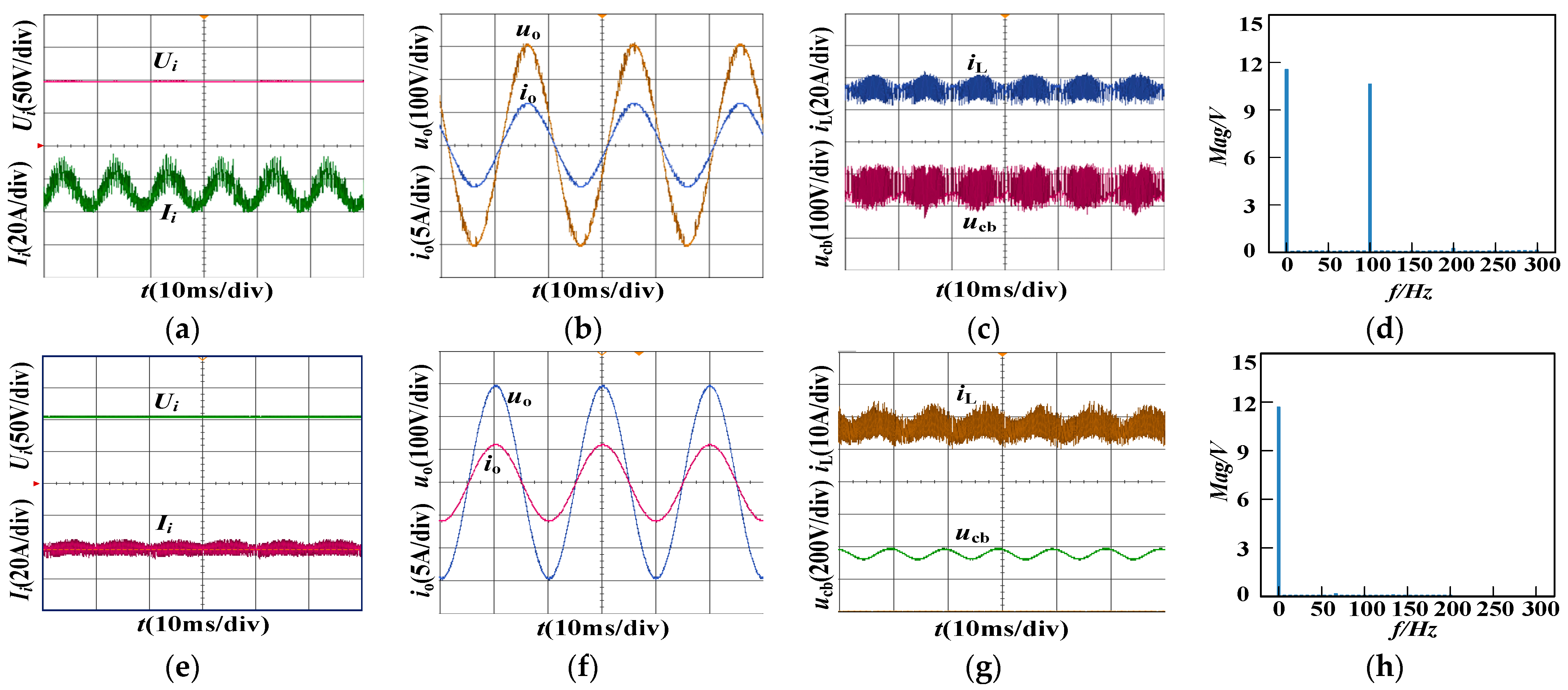
The experimental waveforms of the inverter under the two strategies are shown in Figure 9. Among them, Figure 9a–d represent the experiment waveforms of the proposed inverter using output voltage feedback SPWM control, and Figure 9e–h show the experiment waveforms of the inverter using three-closed-loop composite control that can suppress the low-frequency ripple of the input current. It can be seen from Figure 9 that the proposed inverter under the two control strategies can realize single-stage booster inverters. The three-closed-loop control strategy can realize power decoupling and transfer low-frequency pulsating power on the load side to the buffer capacitor uc, while uc pulsates at twice the frequency near the limit value so as to suppress the low-frequency ripple component of input current and make the input current approximate the DC. It can be seen from Figure 9d,h that the secondary ripple content of the input current before decoupling is 10.13%, and the secondary ripple content of the input current after decoupling is 1.2%.
The steady-state waveforms of the inverter with resistive full load, inductive full load (PF = 0.75), and capacitive full load (PF = 0.75) are shown in Figure 10. The experimental waveforms show that the following: (1) when the inverter is working normally, the buffer capacitor voltage is stable at 360 V and pulsates at double frequency, and the inductor current of the energy storage is stable around 18 A, which is consistent with theoretical analysis and simulation. Due to the actual inductance value, the capacitance value, and the error of the duty cycle generated by DSP, the capacitor voltage and inductor current pulsation are slightly larger than the design value. (2) The proposed inverter is suitable for resistive, resistive–inductive, and resistive–capacitive loads, and the output voltage and current waveforms are of good quality. (3) Figure 10h,I give the high-frequency switching waveforms of the positive and negative half-cycle operating modes of the output voltage and four circuit modes, respectively, where Ta and Tb correspond to the discharge working mode and charging working mode, respectively.
The experimental waveforms of the single-stage, single-phase current source inverter with a source buffer when the load on the output side changes abruptly are shown in Figure 11. The resistive load power changes from 1000 W to 500 W and changes from 500 W to 1000 W, respectively.
It can be seen from the experimental waveforms in Figure 11 that the proposed inverter adopts three-closed-loop composite control with an energy storage inductor current limit and buffer capacitor voltage limit, which has good steady-state and dynamic performance. When the load changes, the inverter state fluctuates slightly, and the output voltage and current can transition quickly and smoothly. The experimental results are basically consistent with theoretical analysis and simulation, which verify the correctness and feasibility of the proposed research scheme.
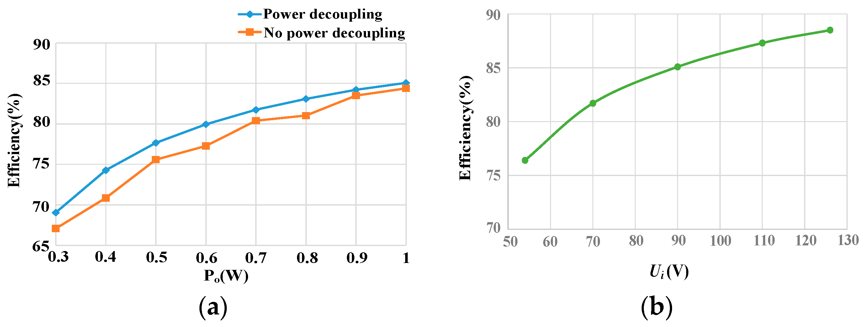
The losses of the proposed converter are mainly inductor loss (copper loss PCu and iron loss PFe) and power device loss (switching loss PSw and on-state loss PS-on). Due to the inductor loss, because the inductor current is dominated by the DC component and the value is large, PCu is much larger than PFe, and the inductor loss is approximately equal to PCu, while PCu basically does not change with the output power Po. In power device loss, PSw depends on the number of switches of the switch action, frequency, voltage stress, and current stress when the circuit mode is switched. PS-on depends on the number of switch conductions, the conduction time, the on-state current, and internal resistance in each circuit mode. Under different Po, the operating modes that switch by each high-frequency switching cycle are roughly the same (i.e., the number of switches working is the same), and the switching frequency and input/output voltage are basically unchanged (i.e., the voltage stress is unchanged). Considering that the inductor current is approximately DC, the influence of other factors is basically unchanged except when the output current causes PS-on increases with Po. Figure 12 shows the efficiency of the system before and after power decoupling under resistive load and the efficiency of the input voltage Ui change under full load. In Figure 12a, the efficiency increases with the increase in output power in both cases. This is because when Po is low, the inherent loss PCu is dominant. As Po increases, the proportion of PCu decreases. Meanwhile, Po increases, and the duty cycle of the magnetization mode and the energy-feeding mode increases, resulting in a significant increase in PS-on, so the rate of increase in efficiency decreases. In addition, because the inverter bridge uses four blocking diodes, which bring a certain proportion of system loss, with the development of the reverse–resistance device, these blocking diodes can be omitted so that the system efficiency can be greatly improved.
In Figure 12b, the efficiency increases with the increase in input voltage Ui. From (17), it can be seen that as Ui increases, the inductor current limit value decreases, resulting in a decrease in PCu. At the same time, the duty cycle of the inductance magnetization mode decreases, and the duty cycle of the energy-feeding mode increases slightly. Therefore, PS-on decreases, while PSw does not change significantly, so the efficiency increases.
Table 4 shows the comparison of several research schemes. In [21], the proposed scheme uses a thin film capacitor to replace the electrolytic capacitor, which greatly reduces the capacitance value of the buffer capacitor; the inductance parameter is small and has good secondary ripple suppression ability. However, the control strategy is complex, the boost ratio is low, and experimental data such as efficiency, output voltage THD, and dynamic response time are not given. The scheme proposed in [23] suppresses the low-frequency ripple of the input current to a certain extent, but the control method is complex, and the relevant data of the experimental results are not given. The control method used in [24] is relatively simple, the system efficiency is high, and the output dynamic response time is fast when the load changes abruptly. However, the number of energy storage elements is the largest, and the value is the largest, and the experimental data, such as the second harmonic content and the output voltage THD, are not given. In [28], the proposed scheme has fewer components, higher system efficiency, and faster dynamic response time, but the secondary ripple content of the input current and the output voltage THD are relatively high. The control method proposed in this paper is simple: the output voltage THD and input current second harmonic content are low, and the dynamic performance is good, but the system efficiency is low. With the development of the reverse resistance device, the reverse resistance device can be used to replace the MOS tube of the inverter bridge of the proposed circuit in the future, and four blocking diodes can be removed, which significantly reduces the loss of the power device and makes the system’s obtain better overall efficiency.

7. Conclusions

  • The circuit topology of the single-stage boost source single-phase inverter is proposed, which is mainly composed of the energy storage inductor, active buffer circuit, and single-phase current source inverter bridge and filter. The active buffer circuit provides the hardware conditions for the inverter energy feedback and input and output power decoupling, so the circuit has the ability of a single-stage boost inverter and can undertake the low-frequency ripple suppression of the input current.
  • A three-closed-loop composite control strategy is proposed under the limitation of the inductor current and buffer capacitor voltage, and the limit values of the inductor current and buffer capacitor voltage are derived, respectively, according to the circuit boost transformation mechanism and working mode characteristics.
  • The proposed inverter has four circuit modes in the boost stage, where the energy storage inductor can be demagnetized through the energy feed mode, and the circuit mainly works in the magnetizing mode and the energy feed mode. In the buck stage of the inverter, the energy storage inductor can only be demagnetized by the buffer capacitor, and the circuit mainly works in the buffer capacitor charging and discharging modes.
  • The circuit parameters of the proposed inverter are analyzed and designed. The mathematical model of the inverter is established from the perspective of energy conservation, combined with the state space average method, and the controller parameters of the system are designed. The simulation and experiments show that the proposed inverter is equipped with good input current low-frequency ripple suppression and single-stage boost conversion capability. It has a simple circuit and control, the output voltage THD is low, and can adapt to various types of loads, such as resistive, resistive-inductive, and resistive-capacitive load, and has a good steady state and dynamic performance.

Author Contributions

Conceptualization, Y.W.; investigation Z.J., X.T., T.L. and B.J.; methodology, Y.W. and T.L.; validation X.T.; formal analysis Z.J. and K.Q.; data curation B.J.; writing—original draft preparation, Z.J.; writing—review and editing, X.T. and T.L.; visualization, B.J.; supervision, K.Q. project administration, Y.W.; funding acquisition, Y.W. All authors have read and agreed to the published version of the manuscript.

Funding

This research was funded by the Education Department of Hunan Province (grant number 22A0476).

Data Availability Statement

Data are contained within the article.

Conflicts of Interest

The authors declare no conflicts of interest.

References

  1. Prasad, K.R.; Madhavi, S.V.; Satyanarayana, A.V.; Mallam, M.; Prasad, J.S.; Suman, J.V. Design and Management of an Integrated Solar-Wind Conversion System Using DFIG. In Proceedings of the 2024 International Conference on Advances in Modern Age Technologies for Health and Engineering Science (AMATHE), Shivamogga, Karnataka, India, 9–10 May 2024; pp. 1–6. [Google Scholar]
  2. Tang, M.; Li, J.; Qiu, J.; Guo, X.; An, B.; Zhang, Y.; Wang, W. MPPT Strategy of Waterborne Bifacial Photovoltaic Power Generation System Based on Economic Model Predictive Control. Energies 2023, 17, 152. [Google Scholar] [CrossRef]
  3. Blaabjerg, F.; Yang, Y.; Kim, K.A.; Rodriguez, J. Power Electronics Technology for Large-Scale Renewable Energy Generation. Proc. IEEE 2023, 111, 335–355. [Google Scholar] [CrossRef]
  4. Rakib, K.; Salimullah, S.M.; Hossain, M.S.; Chowdhury, M.A.; Ahmed, J.S. Stability Analysis of Grid Integrated BESS Based Hybrid Photovoltaic (PV) and Wind Power Generation. In Proceedings of the 2020 IEEE Region 10 Symposium (TENSYMP), Dhaka, Bangladesh, 5–7 June 2020; pp. 1717–1720. [Google Scholar]
  5. Chen, Y.; Jiang, Z.; Wei, L.; Zhang, Y.; Jiang, J. An Asymmetric Full-Bridge Bidirectional DC–AC Converter With Power Decoupling and Common-Mode Current Suppression for V2G Application. IEEE J. Emerg. Sel. Top. Power Electron. 2024, 12, 2870–2881. [Google Scholar] [CrossRef]
  6. Nie, L.; Zhu, G.; Luo, B.; Qi, E.; Zeng, D.; Huang, S. A Novel Control Method for the Active Power Decoupling Module with Plug-and-Play in Single Phase Inverter. In Proceedings of the 2018 IEEE International Power Electronics and Application Conference and Exposition (PEAC), Shenzhen, China, 4–7 November 2018; pp. 1–6. [Google Scholar]
  7. Xu, S.; Chang, L.; Shao, R. Single-Phase Voltage Source Inverter With Voltage Boosting and Power Decoupling Capabilities. IEEE J. Emerg. Sel. Top. Power Electron. 2020, 8, 2977–2988. [Google Scholar] [CrossRef]
  8. Rekha, Y.; Christopher, I.W.; Jamuna, V. Fuel Cell Based Sl Quasi Z-Source Inverter for Motor Drive. In Proceedings of the 2019 Fifth International Conference on Electrical Energy Systems (ICEES), Chennai, India, 21–22 February 2019; pp. 1–6. [Google Scholar]
  9. Hwang, D.-H.; Lee, J.-Y.; Cho, Y. PCC Voltage Compensation of PV Inverter with Active Power Decoupling Circuit. In Proceedings of the 2018 International Power Electronics Conference (IPEC-Niigata 2018-ECCE Asia), Niigata, Japan, 20–24 May 2018; pp. 1403–1408. [Google Scholar]
  10. Seta, Y.; Shimizu, T. Low Power Factor Operation of PV Inverter with Power Decoupling Function. In Proceedings of the 2016 IEEE Energy Conversion Congress and Exposition (ECCE), Milwaukee, WI, USA, 18–22 September 2016; pp. 1–6. [Google Scholar]
  11. Emar, W.; Issa, H.; Kanaker, H.; Fares, O.; Attar, H. A New Double-Switch SEPIC-Buck Topology for Renewable Energy Applications. Energies 2024, 17, 238. [Google Scholar] [CrossRef]
  12. Jain, S.; Shadmand, M.B.; Balog, R.S. Decoupled Active and Reactive Power Predictive Control for PV Applications Using a Grid-Tied Quasi-Z-Source Inverter. IEEE J. Emerg. Sel. Top. Power Electron. 2018, 6, 1769–1782. [Google Scholar] [CrossRef]
  13. Sabeeh Al-Obaidi, S.A.; Hodge, K.C.; Enjeti, P. A Dual-Phase Output 4-Leg Inverter with Active Decoupling and Integrated Power Optimizer for Off-Grid Applications. In Proceedings of the 2018 9th IEEE International Symposium on Power Electronics for Distributed Generation Systems (PEDG), Charlotte, NC, USA, 25–28 June 2018; pp. 1–6. [Google Scholar]
  14. SeyyedHosseini, M.; Yazdian-Varjani, A.; Mohamadian, M. Power Decoupling Method for Single Stage Current Fed Flyback Micro Inverter. In Proceedings of the 2020 11th Power Electronics, Drive Systems, and Technologies Conference (PEDSTC), Tehran, Iran, 4–6 February 2020; pp. 1–6. [Google Scholar]
  15. Wickramasinghe Abeywardana, D.B.; Acuna, P.; Hredzak, B.; Aguilera, R.P.; Agelidis, V.G. Single-Phase Boost Inverter-Based Electric Vehicle Charger With Integrated Vehicle to Grid Reactive Power Compensation. IEEE Trans. Power Electron. 2018, 33, 3462–3471. [Google Scholar] [CrossRef]
  16. Chen, J.; Hu, H.; Wang, M.; Ge, Y.; Wang, K.; Huang, Y.; Yang, K.; He, Z.; Xu, Z.; Li, Y.R. Power Flow Control-Based Regenerative Braking Energy Utilization in AC Electrified Railways: Review and Future Trends. IEEE Trans. Intell. Transp. Syst. 2024, 25, 6345–6365. [Google Scholar] [CrossRef]
  17. Chen, J.; Zhao, Y.; Wang, M.; Wang, K.; Huang, Y.; Xu, Z. Power Sharing and Storage-Based Regenerative Braking Energy Utilization for Sectioning Post in Electrified Railways. IEEE Trans. Transp. Electrif. 2024, 10, 2677–2688. [Google Scholar] [CrossRef]
  18. Li, T.; Shi, Y. Application of MMC-RPC in High-Speed Railway Traction Power Supply System Based on Energy Storage. Appl. Sci. 2022, 12, 10009. [Google Scholar] [CrossRef]
  19. Kan, S.; Ruan, X.; Dang, H.; Zhang, L.; Huang, X. Second Harmonic Current Reduction in Front-End DC−DC Converter for Two-Stage Single-Phase Photovoltaic Grid-Connected Inverter. IEEE Trans. Power Electron. 2019, 34, 6399–6410. [Google Scholar] [CrossRef]
  20. Zhang, L.; Ruan, X.; Ren, X. Second-Harmonic Current Reduction and Dynamic Performance Improvement in the Two-Stage Inverters: An Output Impedance Perspective. IEEE Trans. Ind. Electron. 2015, 62, 394–404. [Google Scholar] [CrossRef]
  21. Zhang, Y.; Fu, W.; He, P. A Novel Power Decoupling Circuit in Paralleled with AC Side in Photovoltaic Micro-Inverter. In Proceedings of the 2019 14th IEEE Conference on Industrial Electronics and Applications (ICIEA), Xi’an, China, 19–21 June 2019; pp. 821–826. [Google Scholar]
  22. Watanabe, H.; Itoh, J.; Iwabuchi, A. Experimental Verification of DC to Single-Phase AC Converter with Power Decoupling Capability Using 1.2 kV SiC-MOSFET Module. In Proceedings of the 2019 IEEE Workshop on Wide Bandgap Power Devices and Applications in Asia (WiPDA Asia), Taipei, Taiwan, 23–25 May 2019; pp. 1–4. [Google Scholar]
  23. Xu, S.; Chang, L.; Shao, R.; Mohomad, A.H. Single-Phase Bridge Inverter with Active Power Decoupling Based on Buck-Boost Converter. In Proceedings of the 2018 IEEE Energy Conversion Congress and Exposition (ECCE), Portland, OR, USA, 23–27 September 2018; pp. 6725–6732. [Google Scholar]
  24. Bodele, N.; Kulkarni, P.S. A Zero-Leakage-Current Single-Stage PV-Battery Integrated Inverter with Active Power Decoupling. IEEE Trans. Circuits Syst. II Express Briefs 2024. [Google Scholar] [CrossRef]
  25. Kim, J.; Cha, H. Switching Cell Current Source Inverter With Active Power Decoupling Circuit. IEEE Trans. Ind. Electron. 2024, 71, 12183–12191. [Google Scholar] [CrossRef]
  26. Shi, S.; Sun, Y.; Dan, H.; Song, D.; Su, M.; Guo, B.; Tang, H. A General Closed-Loop Power-Decoupling Control for Reduced-Switch Converter-Fed IM Drives. Electr. Eng. 2020, 102, 2423–2433. [Google Scholar] [CrossRef]
  27. Jiang, J.; Sun, H.; Wang, H. A Comprehensive Review of Single-Phase Converter Topologies with 2ω-Ripple Suppress. Electr. Eng. 2024, 106, 225–262. [Google Scholar] [CrossRef]
  28. Tian, H.; Chen, M.; Liang, G.; Xiao, X. A Single-Phase Transformerless Common-Ground Type PV Inverter With Active Power Decoupling. IEEE Trans. Ind. Electron. 2023, 70, 3762–3772. [Google Scholar] [CrossRef]
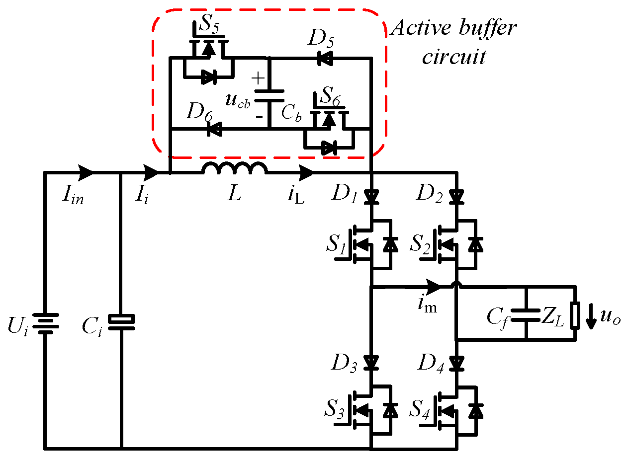
Figure 1. Circuit topology of new single-stage booster single-phase inverter.
Energies 17 04522 g001
Figure 2. Two−target three−closed−loop composite control strategy: (a) System control block diagram; (b) Principle waveform diagram.
Energies 17 04522 g002
Figure 3. Two-loop control block diagram on DC side.
Energies 17 04522 g003
Figure 4. Output voltage loop control block diagram.
Energies 17 04522 g004
Figure 5. Comparison of key waveforms at full load for two control strategies: (a) Ui, Ii; (b) resistive load uo, io; (c) ucb, iL; (d) Ii THD; (e) Ui, Ii; (f) resistive load uo, io; (g) ucb, iL; and (h) Ii THD.
Energies 17 04522 g005
Figure 6. Output full−load simulation waveform: (a) resistive load uo, io; (b) S1, S3 voltage stress; (c) S2, S4 voltage stress; (d) S5, S6 voltage stress; (e) positive half−cycle mode switching; (f) negative half−cycle mode switching; (g) resistive−inductive load uo, io; and (h) resistive−capacitive load uo, io.
Energies 17 04522 g006
Figure 7. Dynamic simulation waveform of sudden load change: (a) Ui, Ii (1000 W→500 W); (b) uo, io (1000 W→500 W); (c) ucb (1000 W→500 W); (d) iL (1000 W→500 W); (e) Ui, Ii (1000 W→500 W); (f) uo, io (1000 W→500 W); (g) uc (500 W→1000 W); and (h) iL (500 W→1000 W).
Energies 17 04522 g007
Figure 8. Experimental device for circuit topology of new single-stage booster single-phase inverter.
Energies 17 04522 g008
Figure 9. Waveform comparison before and after decoupling: (a) Ui, Ii; (b) resistive load uo, io; (c) ucb, iL; (d) Ii THD; (e) Ui, Ii; (f) resistive load uo, io; (g) ucb, iL; and (h) Ii THD.
Energies 17 04522 g009
Figure 10. Full-load steady-state experimental waveform: (a) resistive load uo, io; (b) S1, S3 drive and stress; (c) high-frequency expansion of S1, S3; (d) S2, S4 drive and stress; (e) high-frequency expansion of S2, S4; (f) S5, S6 drive and stress; (g) high-frequency expansion of S5, S6; (h) positive half-cycle mode switching; (i) negative half-cycle mode switching; (j) inductive load uo, io; and (k) resistive capacitance load uo, io.
Energies 17 04522 g010
Figure 11. Waveform of load jump experiment: (a) Ui, Ii (1000 W→500 W); (b) uo, io (1000 W→500 W); (c) uc, iL (1000 W→500 W); (d) Ui, Ii (500 W→1000 W); (e) uo, io (500 W→1000 W); and (f) uc, iL (500 W→1000 W).
Energies 17 04522 g011
Figure 12. System efficiency: (a) efficiency before and after power decoupling; (b) efficiency of input voltage variation.
Energies 17 04522 g012
Table 1. Output voltage feedback drive logic signal under SPWM control.
Circuit StatusHigh-Frequency-Switching IntervalS1S2S3S4S5S6
uo > 0, iL < IL*, ucb < Ucb*(1 – d)TS101000
dTS100100
uo > 0, iL < IL*, ucb > Ucb*(1 – d)TS000011
dTS100100
uo > 0, iL > IL*(1 – d)TS000000
dTS100100
uo < 0, iL < IL*, ucb < Ucb*(1 – d)TS101000
dTS011000
uo < 0, iL < IL*, ucb > Ucb*(1 – d)TS000011
dTS011000
uo < 0, iL > IL*(1 – d)TS000000
dTS011000
Table 2. Drive logic signal under two target three-closed-loop compound controls.
isy0isy1isy2isy3S1S2S3S4S5S6
1x11101000
1x10100100
110x000000
100x000011
0x11010100
0x10011000
010x000000
000x000011
Table 3. Key parameters of circuit.
Circuit ParametersNumerical Values
Rated capacity S/VA1000
Rated output voltage RMS Uo/V220
Input voltage Ui/V90
Energy storage inductor L/mH1.5
Buffer capacitor Cb/uF120
Input filter capacitor Ci/uF200
Output filter capacitor Cf/uF16.8
Switching frequency f/kHz50
Table 4. Performance comparison among the converters.
Parameters[21][23][24][28]Proposed
No. of levels21111
No. of switches126756
No. of diodes10016
Capacitance20 µF/10 µF100 µF/10 µF170 µF/220 µF/220 µF22 µF120 µF/200 µF/16.8 µF
Inductance70 µH/10 mH300 µH/0.8 mH2.5 mH/1.8 mH30 µH/1.5 mH1.5 mH
Control complexityComplexComplexMediumMediumSimple
Boost levelSmallMediumLargerLargerLarger
Rated power500 W400 W1000 W320 W1000 W
Secondary ripple content1.73%--3.67%1.2%
Efficiency--96.3%95.8%85%
Output voltage THD --5.62%1.5%
Output dynamic response time--40 ms25 ms3 ms
“-” Denotes that the metric was not provided in the reference.
Disclaimer/Publisher’s Note: The statements, opinions and data contained in all publications are solely those of the individual author(s) and contributor(s) and not of MDPI and/or the editor(s). MDPI and/or the editor(s) disclaim responsibility for any injury to people or property resulting from any ideas, methods, instructions or products referred to in the content.