Article

Research on Solid-State Linear Transformer Driver Power Source Driving Atmospheric Pressure Plasma Jet Treatment of Epoxy Resin

1
State Key Laboratory of Reliability and Intelligence of Electrical Equipment, Hebei University of Technology, Tianjin 300401, China
2
University of Chinese Academy of Sciences, Beijing 100049, China
*
Author to whom correspondence should be addressed.
Energies 2024, 17(18), 4749; https://doi.org/10.3390/en17184749
Submission received: 5 August 2024 / Revised: 2 September 2024 / Accepted: 8 September 2024 / Published: 23 September 2024
(This article belongs to the Section F: Electrical Engineering)

Abstract

:
The Solid-State Linear Transformer Driver (SSLTD) is a nanosecond pulse power source characterized by its fast rise time and adjustable output waveform. It can generate uniform and stable atmospheric plasma jets, which is suitable for material surface modification. In this study, a 15-stage SSLTD was designed and assembled, which can produce a stable nanosecond pulse voltage up to 15 times the amplitude of the charging voltage at high frequencies, with a rise time of approximately 10 ns. This device can be used to generate stable atmospheric pressure Ar plasma jets with an electron density in the range of 1015~1016 cm−3 and gas temperatures close to room temperature. After the modification treatment by the plasma jets, the content of the C=O groups on the surface of the epoxy resin significantly increased in the wavelength range of 1720~1740 cm−1, and its flashover resistance was noticeably enhanced. The optimal comprehensive modification effect was achieved at a charging voltage of 600 V, pulse width of 50 ns, and pulse frequency in the range of 800~1000 Hz.

1. Introduction

In recent years, plasma technology has developed rapidly, and the generation and application of atmospheric pressure plasma have become hot topics in the field of plasma [1,2]. Plasma can be divided into high-temperature plasma and low-temperature plasma, in which the low-temperature plasma has a significant difference between the electron temperature and ion temperature, characterized by high electron energy and low gas temperature. This minimizes adverse effects on materials and can facilitate some chemically demanding reactions under conventional conditions. Low-temperature plasma jets can precisely act on specific areas, showing great potential in applications that require localized fine processing or operation in confined spaces, such as biomedicine and material surface modification [3,4,5,6].
Common power sources used to drive plasma generation include DC power sources, AC power sources, and pulsed power sources. Compared with traditional AC and DC excitation discharge, a nanosecond pulse power source for material surface modification has unique advantages. On the one hand, nanosecond pulse discharge plasma is more uniform. The ultra-fast rise time in the nanosecond range generates a strong equivalent electric field, rapidly energizing electrons and greatly enhancing gas ionization and excitation, producing many active radicals. On the other hand, due to the narrow pulse width, the discharge channel heating time is in the nanosecond range, while other heavier particles remain at room temperature and do not evolve into equilibrium plasma. This results in high electron energy with low ohmic heating and energy consumption, allowing for simplified or eliminated electrode cooling systems and a simplified discharge system structure, facilitating discharge control [1,7]. Notably, the generation time of low-temperature plasma is in the nanosecond range. By varying the pulse repetition frequency of the nanosecond pulse power source, the plasma can be fully exposed to the material’s surface, promoting plasma chemical processes and allowing for the precise control of the plasma chemical process time, which is unattainable with other power source forms. Research on material modification using nanosecond pulse power supplies has become a focal point for many researchers. BUNIN I Z used short-term (10~30 s) nanosecond pulsed dielectric barrier discharge and low-temperature plasma under atmospheric pressure to reduce the adsorption and flotation activity of magnetic pyrite, which is beneficial for the removal of sulfides in the metallurgical industry [8]. Lada Z.G effectively increased the regeneration rate of SERS solid substrates in gas and liquid using nanosecond pulsed dielectric barrier discharge plasma, with the degradation rate being the fastest in gas [9]. Attri Pankaj enhanced the efficiency of polymer solar cells by modifying graphene oxide (GO) sheets using nanosecond pulsed plasma [10]. Zhang Cheng used nanosecond pulse diffuse discharge to treat the surface of copper metal, achieving oxidation and increasing its surface hardness [11]. These studies demonstrate that nanosecond pulse power supplies are efficient excitation sources for plasma surface modification and have been applied to material surface modification.
The SSLTD power source is a nanosecond pulse power source based on inductive stacking technology, featuring high repetition rates, controllable switching, high reliability, and a long lifespan [12,13,14]. Compared to other pulse methods, the SSLTD’s parallel switch structure and low inductance in the discharge circuit enable faster pulse rise times. Additionally, the modular design allows for the generation of waveforms of any shape based on the switching times, and a fault in a single module does not affect the operation of other modules [15,16]. Currently, various circuit topologies of SSLTDs have been developed. Y. Wang and L. designed an SSLTD based on a full-bridge module that can produce bipolar nanosecond pulses. However, the leakage inductance of the magnetic core led to an output pulse rise time exceeding 20 ns [17]. Jiang Weihua designed a 30-stage stacked SSLTD with an output voltage of up to 29 kV and a pulse rise time (10–90%) of 30–40 ns [18]. With continuous innovation and optimization in pulse power technology, the plasma generated by SSLTD has been applied in environmental pollution control and biomedicine, but research on material modification is still limited [19,20]. Additionally, low-temperature plasma also exhibits significant application potential in the field of energy conversion. Plasma generated by SSLTD driving can be utilized for energy conversion.
This paper uses a laboratory-developed 15-stage SSLTD to excite low-temperature argon plasma jets, diagnosing and analyzing the emission spectrum of the plasma jet. Additionally, surface modification of the epoxy resin sheets was performed by adjusting the power source parameters (charging voltage, pulse width, and pulse frequency), and the modification effects were evaluated using FTIR analysis and flashover testing. The experimental results indicate that the plasma jet excited by the SSLTD power source effectively enhances the DC flashover field strength on the surface of the epoxy resin sheets, providing a stable and efficient nanosecond pulse power source for material surface modification, which holds significant practical value.

2. Experimental Setup and Measurements

2.1. Principles and Design of SSLTD

The equivalent circuit diagram of the SSLTD is shown in Figure 1a. During its operation, the SSLTD can be considered as a 1:1 pulse transformer. The primary side of the transformer uses a parallel structure consisting of multiple SSLTD modules. Each module has a diode connected between the high-voltage and low-voltage terminals. This diode serves two important functions in the circuit: firstly, it provides a charging path for the capacitor during the charging phase; secondly, it acts as a bypass for non-triggered modules during the discharge phase, enabling modulation of the pulse output waveform. The secondary side of the transformer uses a series structure, where the outputs of each module are summed. At this point, the output voltage of the secondary side is close to the sum of all module voltages, while the output current remains the same as that of a single module [21]. Figure 1b depicts the cross-sectional structure of the SSLTD modules. Each SSLTD module requires an external main capacitor charging voltage, gate drive voltage (12 V), and gate trigger signal (fiber input). To avoid core saturation after multiple pulses, an external circuit with DC reset (2 A) is employed.
The SSLTD used in this experiment consists of 15 modules, with the structural diagram of a single module and the 15-stage SSLTD device shown in Figure 1c,d. As shown in Figure 1a, each module includes ten switch-capacitor branches arranged in a circular pattern around the core, and the specifications and quantities of the main components are listed in Table 1. The maximum voltage of a single module is limited by the voltage of each component, with the maximum output voltage of a single module not exceeding 1 kV.

2.2. Experimental Method

The experimental samples used were G10 epoxy resin sheets with dimensions of 40 mm × 40 mm × 0.2 mm. Before the experiment, the samples were cleaned by wiping with anhydrous ethanol and then placed in a 30 °C constant temperature drying oven for 2 h.
The experimental system for modifying the plasma jet excited by the SSLTD is shown in Figure 2. The Teslaman TD2202 high-voltage DC source is used to charge the internal capacitors of the SSLTD. The DG645 signal generator provides trigger signals to the SSLTD through the signal driver board while also adjusting the width and frequency of the pulse signals. The MAISHENG MS-1201D DC source supplies approximately 4.5 V of driving voltage to the signal driver board. The MAISHENG MN-1003D DC source provides approximately 12 V of gate drive voltage to the SSLTD circuit board. A DC demagnetizing device with a current of 2 A is used to protect the core from saturation.
The experiment tested the load-driving capability of the SSLTD under different parameters, setting the SSLTD charging voltage to a range from 600 to 800 V (a stable plasma jet needs to be generated at high frequencies of 600 Hz and above when the charging voltage is 550 V), the pulse frequency from 200 to 1000 Hz, and the pulse width from 50 to 100 ns. The emission spectra of the plasma jet driven by the SSLTD were obtained using an Ocean Optics QE65000 spectrometer. To ensure that the collected spectrum is the emission spectrum of the plasma on the surface of the epoxy resin, the fiber optic probe was placed in close contact with the epoxy resin sample at a distance of 10 mm from the plasma.
In the plasma modification of epoxy resin, 99.999% pure argon was used as the diluent and carrier gas. The precursor was atomized, diluted, and delivered to the jet tube using an aerosol generator. Under the influence of the plasma, physical and chemical reactions occurred with the epoxy resin. To achieve stable excitation of the plasma jet by the solid-state SSLTD, the flow rate of argon for dilution was set to 10 L/min, and the flow rate of argon for carrying the Benzyl methacrylate precursor was set to 25 L/h. The bottom of the jet tube was positioned 5 mm from the sample’s surface, and the treatment time was consistently 5 min. After processing, flashover testing was conducted using a copper finger electrode. The high-voltage and ground electrodes had a diameter of 20 mm each, with an electrode gap of 5 mm. The rise rate of the DC power supply voltage was controlled by a computer at 2 kV/s.

3. Experimental Results Analysis and Discussion

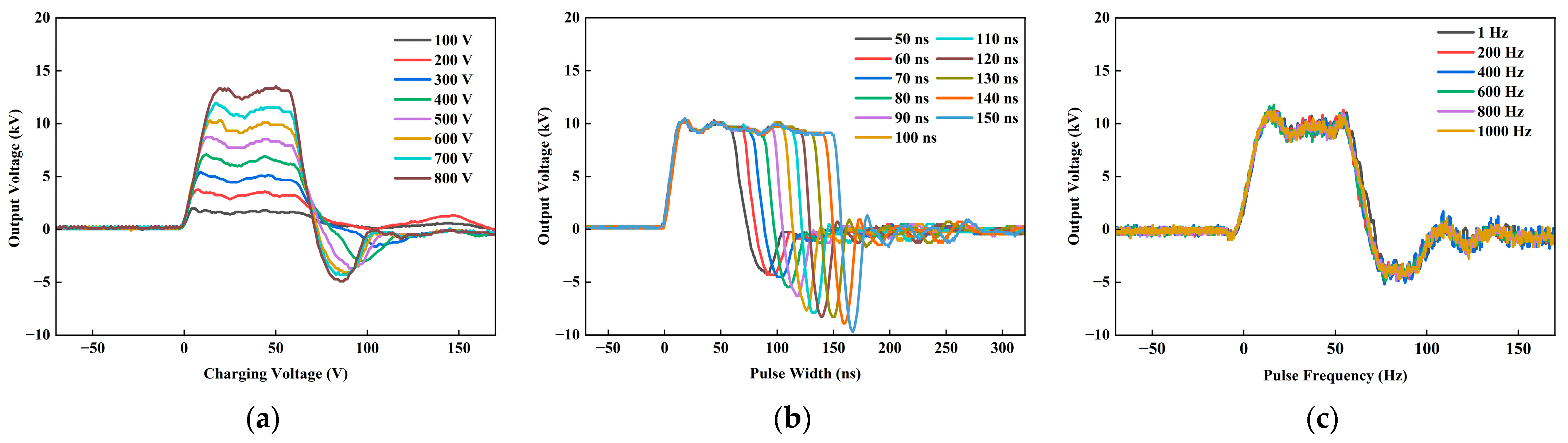
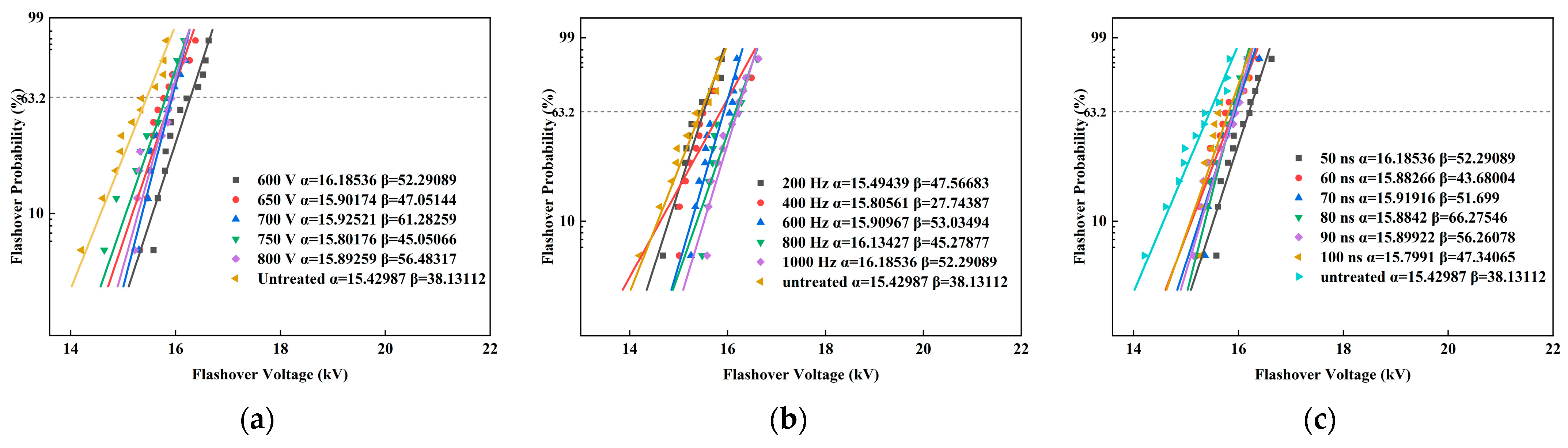
3.1. Performance Testing of SSLTD

Figure 3a shows the output voltage waveforms obtained at different charging voltages. The pulse width of the gate signal controlling the MOSFET is kept constant at 50 ns, with a pulse frequency of 1 Hz. As the charging voltage gradually increases from 100 V to 800 V, the output voltage amplitude rises from approximately 1.5 kV to nearly 14 kV, effectively validating the voltage stacking effect of the SSLTD module. Additionally, due to the influence of the resonance phenomena, the ratio of the output voltage to the input voltage amplitude exceeds the number of stages in the 15-stage SSLTD circuit board.
Figure 3b shows the output voltage waveforms obtained under control signals with different pulse widths. When the pulse width of the control signal increases from 50 ns to 150 ns, the half-width of the output voltage across the load correspondingly increases from approximately 50 ns to about 150 ns. The results indicate that the pulse width of the output voltage from the SSLTD can be continuously adjusted within a certain range by modifying the control signal. The observed rise time of approximately 10 ns is primarily attributed to the time required for the MOSFET driver chip (IXDN630YI) to receive the signal.
Since nanosecond pulse power sources often excite plasma discharges under high repetition frequency conditions, the stability of the power source at high frequencies is particularly important. Figure 3c shows the output voltage waveforms obtained under control signals with different pulse frequencies. It can be observed that as the pulse frequency gradually increases from 1 Hz to 1000 Hz, the output voltage waveform remains mostly consistent, demonstrating the stability of the SSLTD power source under high-frequency conditions.
In summary, the constructed 15-stage SSLTD has the capability to adjust the voltage amplitude, pulse width, and pulse frequency, with the output voltage amplitude exceeding 15 times the charging voltage and a rise time of approximately 10 ns. Furthermore, its performance remains highly stable at high frequencies, with the output voltage waveform essentially unchanged, making it suitable for exciting plasma discharges. However, it is noteworthy that there is a significant oscillation phenomenon at the pulse peak and after the pulse ends. This phenomenon may be related to various factors, such as parasitic inductance in the circuit and stray capacitance, which requires further analysis and research.

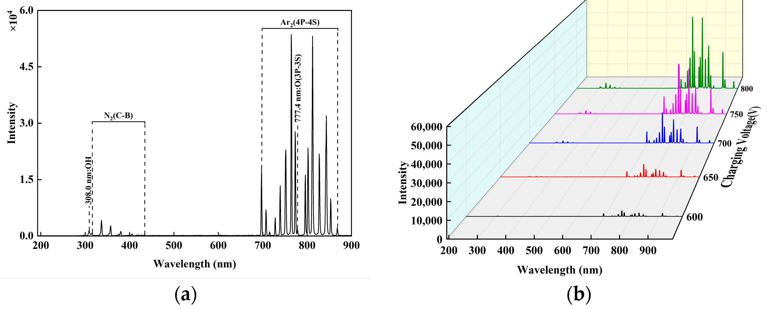
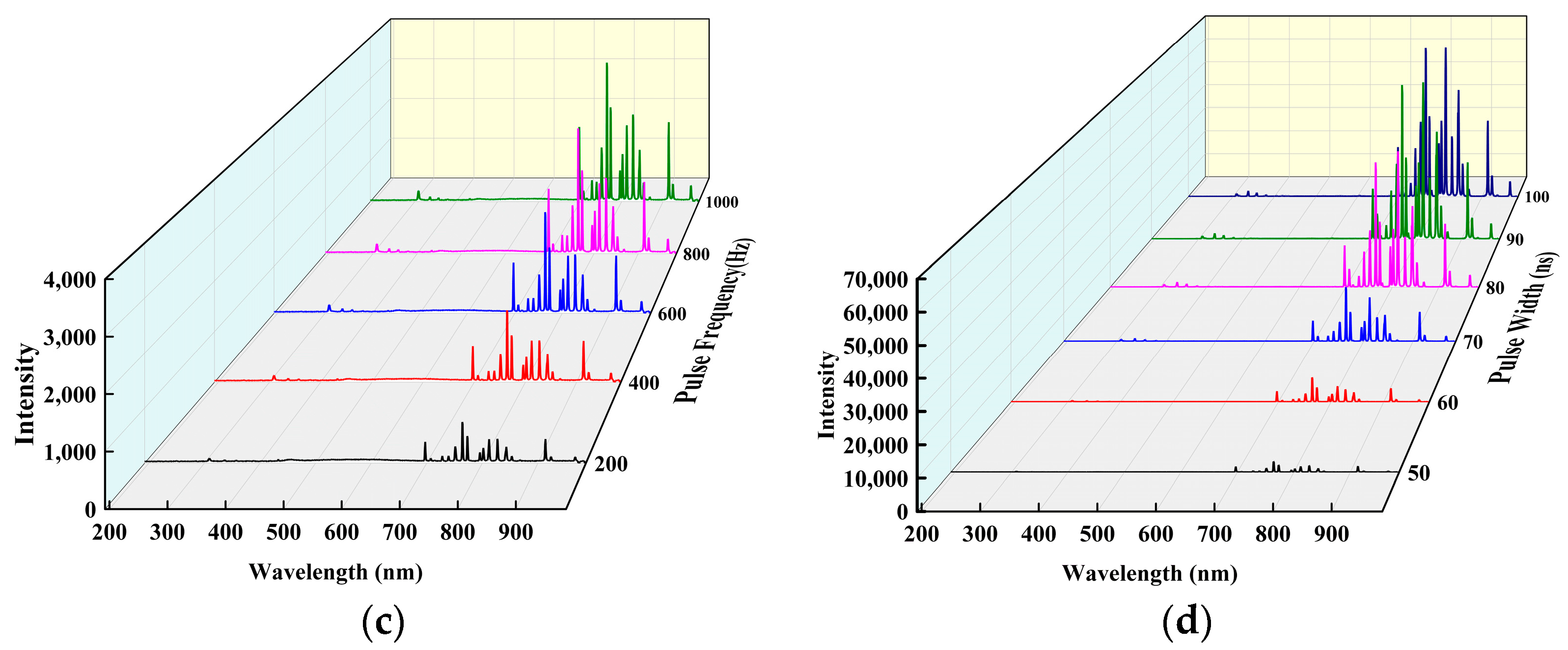
3.2. Optical Characteristics of Atmospheric Pressure Plasma Jet Driven by SSLTD

Figure 4 shows images of plasma jets generated under different experimental conditions using an SSLTD power source. It can be observed that the SSLTD successfully excites a stable plasma jet, and the brightness of the plasma jet increases with higher charging voltage, pulse width, and pulse frequency.
Figure 5a shows the emission spectrum of the plasma jet within the wavelength range of 193~980 nm. It can be observed that the emission spectrum peaks mainly include OH (A→X), N2 (C→B), Ar (4p→4s), and O (3p→3s). The presence of N2 (C→B), OH (A→X) near 308.0 nm and O (3p→3s) near 777.4 nm is attributed to the diffusion of N2 and H2O from the atmospheric environment into the plasma jet, leading to excitation or dissociation phenomena [22].
e + N 2 x e + N 2 A , B , C
e + H 2 O e + H + O H A 2 +
e + O 2 e + O + O
The spectral lines of the Ar (4p→4s) transition in the wavelength range of 680~980 nm primarily originate from the collision of argon atoms with electrons, ionization, and the subsequent collisional–radiative recombination process [23].
e + A r A r 4 p , 4 s + e
e + A r A r + + 2 e
e + A r + A r 4 p , 4 s
e + A r 2 + A r 4 p , 4 s + A r
A r + + A r + A r A r 2 + + A r 4 p , 4 s
Electron density is one of the key parameters reflecting the fundamental characteristics of a plasma, directly influencing the plasma’s dynamic processes and energy transfer efficiency [24]. The Stark broadening method is commonly used to measure the electron density of low-temperature atmospheric pressure plasma jets.
The basic principle of the Stark broadening method is based on the linear response relationship between the Stark broadening of spectral lines in the emission spectrum and the electron density. By analyzing the broadening of the spectral lines measured in experiments, the electron density of the plasma can be calculated after considering Stark broadening. The broadening mechanisms of the atomic emission spectra mainly include Stark broadening (Δλs), instrumental broadening (Δλi), Doppler broadening (ΔλD), and Van der Waals broadening (Δλw). Among these, Δλi and ΔλD are both Gaussian line shapes, corresponding to a broadening of ΔλG, while Δλw and Δλs belong to Lorentzian line shapes, corresponding to a broadening of ΔλL. By performing convolution operations on these two types of line shapes, the Voigt profile function of the atomic emission spectrum can be obtained. Let the linewidth of this spectrum be ΔλV, and then the various broadening mechanisms satisfy the following relationship [25]:
Δ λ w = 3.6 × P / T g 0.7
Δ λ D = 7.16 × 10 7 λ 0 T g / M
Δ λ L = Δ λ s + Δ λ w
Δ λ G = Δ λ D 2 + Δ λ i 2
Δ λ V = Δ λ L 2 2 + Δ λ G 2 1 2 + Δ λ L 2
In the equation, P is the gas pressure, measured in atm; Tg is the gas temperature, measured in K; λ0 is the central wavelength of the spectral line; and M is the relative atomic mass.
Furthermore, the electron density Ne can be calculated using the following formula [26]:
Δ λ S = 2 ω [ 1 + 1.75 α ( 1 c 0 r ) ]
ω = ( N e / N e 0 ) ω n ( T e )
r 9 × 10 3 N e 1 / 6 / T e
α = ( N e / N e 0 ) 1 / 4 α n ( T e )
In the equation, Te is the electron temperature, r is the ratio of the average distance between ions to the Debye length, ω is the half-width due to collisions with electrons, and α is the characteristic of quasi-static ion broadening. The parameters ωn and an, N e 0 = 1016 cm−3, are used to normalize the electron density, expressed in cm−3, and for neutral particles, c0 = 0.75 [27].
In this study, the Ar 738.4 nm spectral line, which is relatively prominent and free from overlap, was used for a straightforward calculation of electron density. The calculation results are as follows. The plasma electron densities at different charging voltages, pulse frequencies, and pulse widths are given in Table 2, Table 3 and Table 4, respectively.
Under the experimental conditions, the electron density of the plasma jet excited by the SSLTD power source is in the range of 1015 to 1016 cm−3. This range avoids both excessively low electron densities, which would result in insufficient plasma jet energy and inadequate interaction with the material surface, leading to insufficient modification effects and excessively high electron densities, which could cause the plasma jet to be too intense, resulting in rapid increases in surface temperature or excessive localized heat, potentially damaging the material and affecting the final modification effect. Additionally, a temperature gun was used to measure the modified area, with an overall temperature ranging from 26 to 33 °C, close to room temperature, indicating no damage to the material surface.
Figure 5b–d show the emission spectra of the plasma jet under different experimental parameters. Overall, the spectral intensity increases consistently with variations in experimental parameters, specifically with increases in the SSLTD power source’s charging voltage, pulse frequency, and pulse width. This is because the increase in the SSLTD charging voltage and pulse width raises the output energy of the SSLTD, resulting in higher expected energy for free electrons, increased electron density, and intensified electron–atom–ion three-body collisions. These effects promote the production of more excited state particles that emit photons, ultimately leading to increased spectral intensity. Although changes in pulse frequency within the range of 200~1000 Hz do not significantly affect electron density, they cause the power source’s energy to be transferred to the plasma more frequently, improving energy deposition efficiency and increasing the number of excited state particles in the plasma jet, which accumulates and increases the spectral intensity.

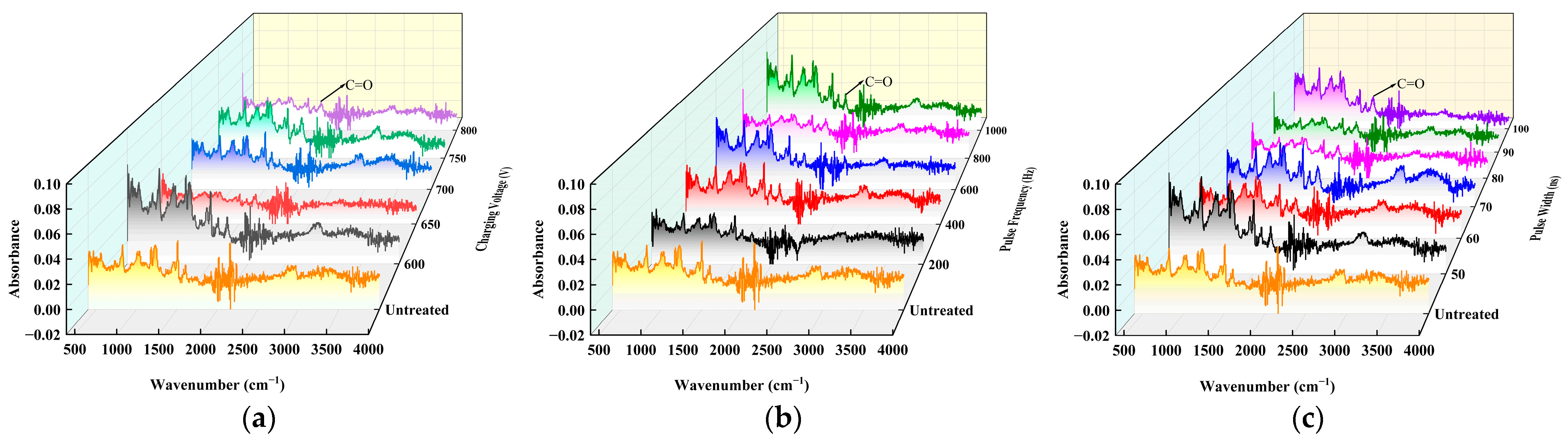
3.3. Analysis of Typical Properties of Epoxy Resin Treated by Atmospheric Pressure Plasma Jet

FTIR can reveal molecular vibrations and provide information about molecular functional groups, making it an essential tool for identifying changes in the molecular structure of epoxy resin surfaces. Figure 6 shows the FTIR results for the central region of epoxy resin treated under different experimental conditions. By comparing the new absorption peaks with the original ones on the epoxy resin surface, the modification effect of the plasma jet is evident. After the modification treatment, the intensity of the C-O absorption peak around 1750 cm−1 on the epoxy resin surface increased significantly, and it showed a trend of further increase with rising pulse frequency. However, with increasing pulse width and charging voltage, the changes became irregular and even slightly decreased.
In response to the aforementioned phenomenon, this paper conducts a comparative study of the modified regions of the samples, as shown in Figure 7. It can be observed that under the experimental conditions of this study, the increase in pulse frequency primarily affects the central part of the modified region, resulting in a more uniform modification effect, while increases in pulse width and charging voltage lead to the outward expansion of the modified region. This paper suggests that this phenomenon is closely related to charge density, and the specific mechanism requires further investigation. It is important to note that due to the influence of the electrode structure, the plasma near the tube wall is more intense than that at the center of the tube, which has a certain impact on the profile of the sample.
Figure 8 shows the variation in the flashover voltage on the surface of the epoxy resin after modification. The results indicate that the surface flashover voltage of untreated epoxy resin sheets is approximately 15.43 kV. After modification, the flashover voltage of the samples increased, and it was found to be consistent with the FTIR detection results of the central area of the modified region. Under the experimental conditions of a charging voltage of 600 V, a pulse width of 50 ns, and a pulse frequency of 1000 Hz, the intensity of the C=O stretching peak near the wavelength range of 1720~1740 cm−1 was the highest, and the flashover voltage reached a maximum value of approximately 16.18 kV, which is similar to that observed at a pulse frequency of 800 Hz.
The excellent insulating properties of epoxy resin make it commonly used in the manufacturing of electronic and electrical equipment. In this paper, the flashover resistance of epoxy resin samples modified by plasma jet treatment has been significantly improved, enhancing the safety and reliability of electrical equipment operation. Specifically, with a charging voltage of 600 V, a pulse width of 50 ns, and a pulse frequency in the range of 800~1000 Hz, the modification effect of the plasma jet was more pronounced.

4. Conclusions

This study designed and built a 15-stage SSLTD power source, and its output characteristics were measured. This power source was used to generate stable Ar plasma jets; whose emission spectra were captured. Subsequently, the plasma jets were used for the modification of epoxy resin, and the flashover experiments evaluated the modification effects. The main conclusions are as follows:
(1)
The designed 15-stage SSLTD can stably output nanosecond pulse voltages with an amplitude 15 times the charging voltage under high-frequency conditions, with a rise time of approximately ten nanoseconds, making it suitable for plasma discharge.
(2)
The SSLTD successfully excited stable Ar plasma jets with temperatures ranging between approximately 26 and 33 °C and electron densities in the range of 1015~1016 cm−3, which can effectively interact with material surfaces while avoiding excessive plasma jet intensity that could damage the materials and affect the final modification outcome.
(3)
In the modification process of the argon plasma jet excited by SSLTD, the increase in pulse frequency primarily affects the central part of the modified region, resulting in a more uniform modification effect. In contrast, increases in charging voltage and pulse width promote the outward expansion of the modified region. After modification, the dielectric breakdown resistance of the epoxy resin surface is significantly enhanced. Optimal modification effects are observed at a charging voltage of 600 V, a pulse width of 50 ns, and a pulse frequency within the range of 800 to 1000 Hz.

Author Contributions

Conceptualization, X.C. and G.S.; methodology, X.C.; validation, X.C., H.C. and Y.C.; formal analysis and investigation, X.C. and Y.C.; resources, X.C. and Y.C.; data curation, X.C. and G.S.; writing—original draft preparation, G.S.; writing—review and editing, G.S. and X.C.; supervision, X.C.; project administration, G.S. All authors have read and agreed to the published version of the manuscript.

Funding

This research received no external funding.

Data Availability Statement

The original contributions presented in this study are included in the article; further inquiries can be directed to the corresponding author.

Conflicts of Interest

The authors declare no conflicts of interest.

References

  1. Shao, T.; Zhang, C.; Wang, R.; Yan, P.; Ren, C. Atmospheric-pressure Pulsed Gas Discharge and Pulsed Plasma Application. High Volt. Eng. 2016, 42, 685–705. [Google Scholar]
  2. Bhuiyan, S.I.; Wang, K.; Baky, M.A.H.; Kraus, J.; Jemison, H.; Staack, D. Controlling Parameters in the Efficiency of Hydrogen Production via Electrification with Multi-Phase Plasma Processing Technology. Energies 2023, 16, 5509. [Google Scholar] [CrossRef]
  3. Nastuta, A.V.; Asandulesa, M.; Doroftei, F.; Dascalu, I.-A.; Varganici, C.-D.; Tiron, V.; Topala, I. Atmospheric Pressure Plasma Jet Exposure of Polylactic Acid Surfaces for Better Adhesion: Plasma Parameters towards Polymer Properties. Polymers 2024, 16, 240. [Google Scholar] [CrossRef] [PubMed]
  4. Svarnas, P.; Poupouzas, M.; Papalexopoulou, K.; Kalaitzopoulou, E.; Skipitari, M.; Papadea, P.; Varemmenou, A.; Giannakopoulos, E.; Georgiou, C.D.; Georga, S.; et al. Water Modification by Cold Plasma Jet with Respect to Physical and Chemical Properties. Appl. Sci. 2022, 12, 11950. [Google Scholar] [CrossRef]
  5. Kikuchi, S.; Saiki, S.; Ohashi, T.; Nakazawa, K. Surface modification for steel rods based on atmospheric-pressure nitrogen plasma treatment at room temperature. Results Mater. 2024, 23, 100612. [Google Scholar] [CrossRef]
  6. Kang, H.; Lee, S.H.; Kim, K. Wettability of polytetrafluoroethylene surfaces by plasma etching modifications. PLoS ONE 2023, 18, 0282352. [Google Scholar] [CrossRef]
  7. Shen, J.; Zhou, Y.; Zhu, X.; Cui, X.; Fang, Z. Enhancement of Ceramic Hydrophobicity with Plasma Jet Excited by AC and Nanosecond Pulse Power Supply. Proc. CSEE 2022, 42, 8781–8791. [Google Scholar]
  8. Bunin, I.Z.; Khabarova, I.A. Comparative study on high-voltage nanosecond pulses and dielectric barrier discharge effects on surface morphology and physico-chemical properties of natural pyrrhotite. J. Phys. Conf. Ser. 2021, 2064, 012056. [Google Scholar] [CrossRef]
  9. Lada, Z.G.; Voyiatzis, G.A.; Aggelopoulos, C.A. A novel, green, low-cost regeneration method for surface enhanced raman scattering (SERS) solid substrates based on nanosecond pulsed cold plasma technology. Surf. Interfaces 2022, 34, 102330. [Google Scholar] [CrossRef]
  10. Attri, P.; Park, J.H.; Gaur, J.; Kumar, N.; Park, D.H.; Jeon, S.N.; Park, B.S.; Chand, S.; Uhm, H.S.; Choi, E.H. Influence of nanosecond pulsed plasma on the non-enzymatic pathway for the generation of nitric oxide from L-arginine and the modification of graphite oxide to increase the solar cell efficiency. Phys. Chem. Chem. Phys. 2014, 16, 18375–18382. [Google Scholar] [CrossRef]
  11. Zhang, C.; Zhou, Z.; Wang, R.; Shen, Y.; Shao, T.; Fang, Z. Modification of Copper Surface by Nanosecond-pulse Diffuse Discharges at Atmospheric Pressure. High Volt. Eng. 2015, 41, 1458–1465. [Google Scholar]
  12. Kazemi, M.R.; Sugai, T.; Tokuchi, A.; Jiang, W. Waveform control of pulsed-power generator based on solid-state LTD. IEEE Trans. Plasma Sci. 2017, 45, 247–251. [Google Scholar] [CrossRef]
  13. Holma, J.; Barnes, M.J. Measurements on a 20-layer 12.5 kV prototype inductive adder for the CLIC DR kickers. In Proceedings of the 2017 IEEE 21st International Conference on Pulsed Power (PPC), Brighton, UK, 18–22 June 2017; pp. 1–5. [Google Scholar]
  14. Woog, D.; Barnes, M.J.; Ducimetière, L.; Holma, J.; Kramer, T. Design of an inductive adder for the FCC injection kicker pulse generator. Physics 2017, 874, 012096. [Google Scholar] [CrossRef]
  15. Yu, F.; Sugai, T.; Tokuchi, A.; Jiang, W. Development of Solid-State LTD Module Using Silicon Carbide MOSFETs. IEEE Trans. Plasma Sci. 2019, 47, 5037–5041. [Google Scholar] [CrossRef]
  16. Jiang, W.; Sugiyama, H.; Tokuchi, A. Pulsed power generation by solid-state LTD. IEEE Trans. Plasma Sci. 2014, 11, 3603–3608. [Google Scholar] [CrossRef]
  17. Wang, Y.; Xu, L.; Jiang, S.; Li, Z.; Rao, J. Solid-State Linear Transformer Driver Based on Full-Bridge Bricks. IEEE Trans. Plasma Sci. 2022, 5, 1269–1275. [Google Scholar] [CrossRef]
  18. Jiang, W. High-frequency Repetitive LTD Based on Semiconductor Switches. High Volt. Eng. 2015, 41, 1776–1780. [Google Scholar]
  19. Zeng, W.; Yu, L.; Dong, S.; Ma, J.; Wang, Y.; He, Y.; Wang, X.; Yao, C. A Novel High-Frequency Bipolar Pulsed Power Generator for Biological Applications. IEEE Trans. Power Electron. 2020, 35, 12861–12870. [Google Scholar] [CrossRef]
  20. Zhao, S.; Hao, C.; Xu, D.; Wen, Y.; Qiu, J.; Liu, K. Effect of electrical parameters on energy yield of organic pollutant degradation in a dielectric barrier discharge reactor. IEEE Trans. Plasma Sci. 2017, 6, 1043–1050. [Google Scholar] [CrossRef]
  21. Feng, Y.; Mao, Y.; Luo, H.; Jiang, W. Performance test and analysisi based on solid-stste high repetitive frequency LTD. High Power Laser Part. Beams 2018, 30, 100–104. [Google Scholar]
  22. Yao, X.; Su, Z.; Gong, D.; Liu, R.; Li, X.; Liu, F.; Jia, P. Study on the Gas Temperature of Atmospheric Pressure Argon Plasma Jet by Spectroscopy. J. Hebei Norm. Univ. (Nat. Sci. Ed.) 2019, 43, 225–229. [Google Scholar]
  23. Tian, F.; Chen, L.; Pei, H.; Bai, J.; Zeng, W. Diagnostic study on jet emission spectroscopy of helium, methane and air plasma under atmospheric pressure. Spectrosc. Spectr. Anal. 2023, 43, 2694–2698. [Google Scholar]
  24. Guo, K.; Zhang, C.; Sun, J.; Chen, G.; Li, J.; Shao, T. Temporal Evolution Characteristics of Discharge Parameters in Insulating Oil Based on Optical Emission Spectra. High Volt. Eng. 2024, 50, 3191–3198. [Google Scholar]
  25. Feng, B.; Wang, R.; Ma, Y.; Zhong, X. Evolution of atmospheric needle-plate discharge plasma. Acta Phys. Sin. 2021, 70, 128–138. [Google Scholar] [CrossRef]
  26. Zeng, X.; Zhang, S.; Bai, H.; Zhang, C.; Shao, T. Electron density calculation of high-voltage discharge plasma based on atomic spectroscopy Stark. Proc. CSEE 2024, 44, 4579–4589. [Google Scholar]
  27. Pellerin, S.; Musiol, K.; Pokrzywka, B.; Chapelle, J. Stark width of 4p’[1/2]-4s [3/2]0 Ar I transition (696.543 nm). J. Phys. B-At. Mol. Opt. Phys. 1996, 29, 3911–3924. [Google Scholar] [CrossRef]
Figure 1. Principles and physical diagram of SSLTD: (a) equivalent circuit of SSLTD; (b) cross-sectional structure of the SSLTD module; (c) single SSLTD module; (d) pulse power generator with 15 SSLTD modules.
Energies 17 04749 g001
Figure 2. Schematic diagram of plasma jet modification experiment driven by the SSLTD.
Energies 17 04749 g002
Figure 3. Performance testing of SSLTD: (a) different charging voltages; (b) different pulse widths of the control signal; (c) different pulse frequencies of the control signal.
Energies 17 04749 g003
Figure 4. Images of plasma jets under different experimental conditions: (a) pulse width 50 ns, pulse frequency 1000 Hz, charging voltage 600~800 V; (b) pulse width 50 ns, charging voltage 600 V, pulse frequency 200~1000 Hz; (c) charging voltage 600 V, pulse frequency 1000 Hz, pulse width 50~100 ns.
Energies 17 04749 g004
Figure 5. Emission spectra of the plasma jet under different experimental conditions: (a) emission spectra of the plasma jet in the wavelength range of 193~980 nm; (b) Ar emission spectra with varying charging voltages; (c) Ar emission spectra with varying pulse frequencies; (d) Ar emission spectra with varying pulse widths.
Energies 17 04749 g005aEnergies 17 04749 g005b
Figure 6. FTIR detection results of epoxy resin: (a) 600~800 V; (b) 200~1000 Hz; (c) 50~100 ns.
Energies 17 04749 g006
Figure 7. Comparison of modified areas of epoxy resin.
Energies 17 04749 g007
Figure 8. Flashover voltage Weibull distribution of epoxy resin: (a) 600~800 V; (b) 200~1000 Hz; (c) 50~100 ns.
Energies 17 04749 g008
Table 1. Specifications and quantities of main components used in SSLTD modules.
DeviceModelValueNumbers
MOSFETC3M0160120J1200 V, 17 A10
Driver-ICIXDN630YI35 V, 30 A10
CapacitorC2220X164KFRL1500 V, 0.16μF30
MagneticCore1k107Outer dia./innerdia./thickness130/86/8 (mm)1
Optical ModuleAFBR-2624ZDC~50 Mbaud1
DiodeSF16001600 V, 1 A (DC)4
Table 2. Electron density of the plasma jet with varying charging voltages.
Charging Voltage (V)600650700750800
Ne (cm−3)4.28 × 10156.24 × 10158.30 × 10159.78 × 10151.31 × 1016
Table 3. Electron density of the plasma jet with varying pulse frequencies.
Pulse Frequency (Hz)2004006008001000
Ne (cm−3)4.35 × 10153.94 × 10154.04 × 10154.59 × 10154.28 × 1015
Table 4. Electron density of the plasma jet with varying pulse widths.
Pulse Width (ns)5060708090100
Ne (cm−3)4.28 × 10155.97 × 10157.83 × 10151.04 × 10161.56 × 10162.28 × 1016
Disclaimer/Publisher’s Note: The statements, opinions and data contained in all publications are solely those of the individual author(s) and contributor(s) and not of MDPI and/or the editor(s). MDPI and/or the editor(s) disclaim responsibility for any injury to people or property resulting from any ideas, methods, instructions or products referred to in the content.

