

Experimental Evaluation of a 2 kW/100 kHz DC–DC Bidirectional Converter Based on a Cuk Converter Using a Voltage-Doubler Concept
 , , and
Abstract
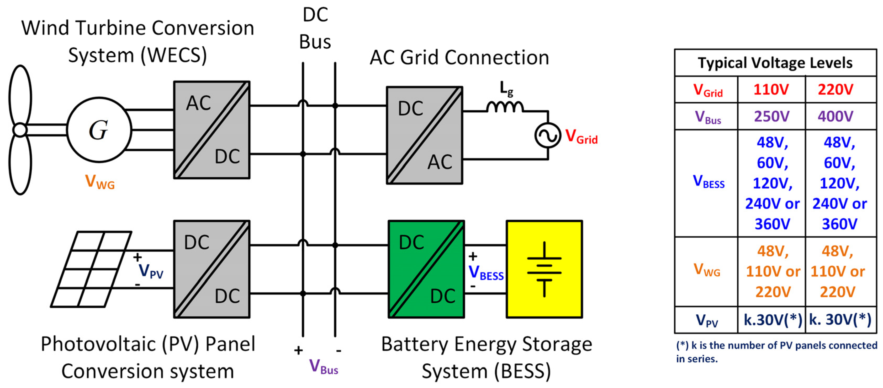
:1. Introduction
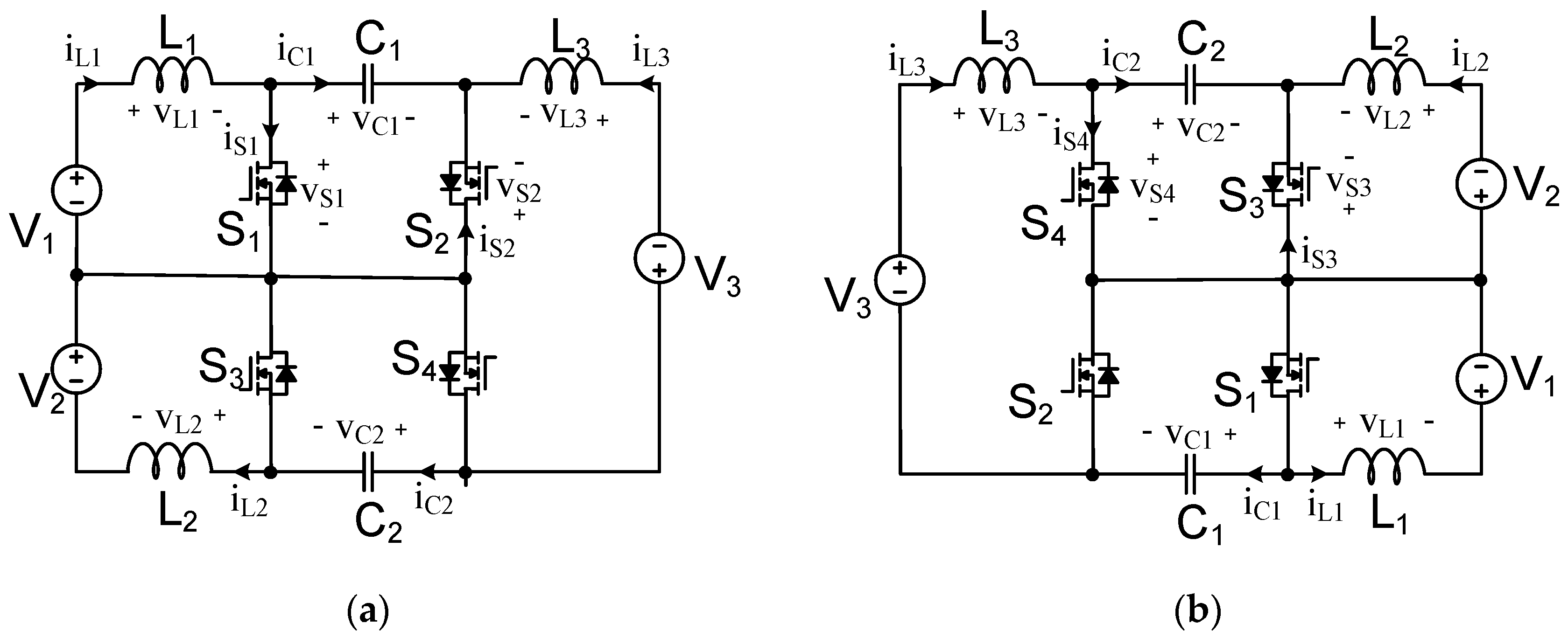
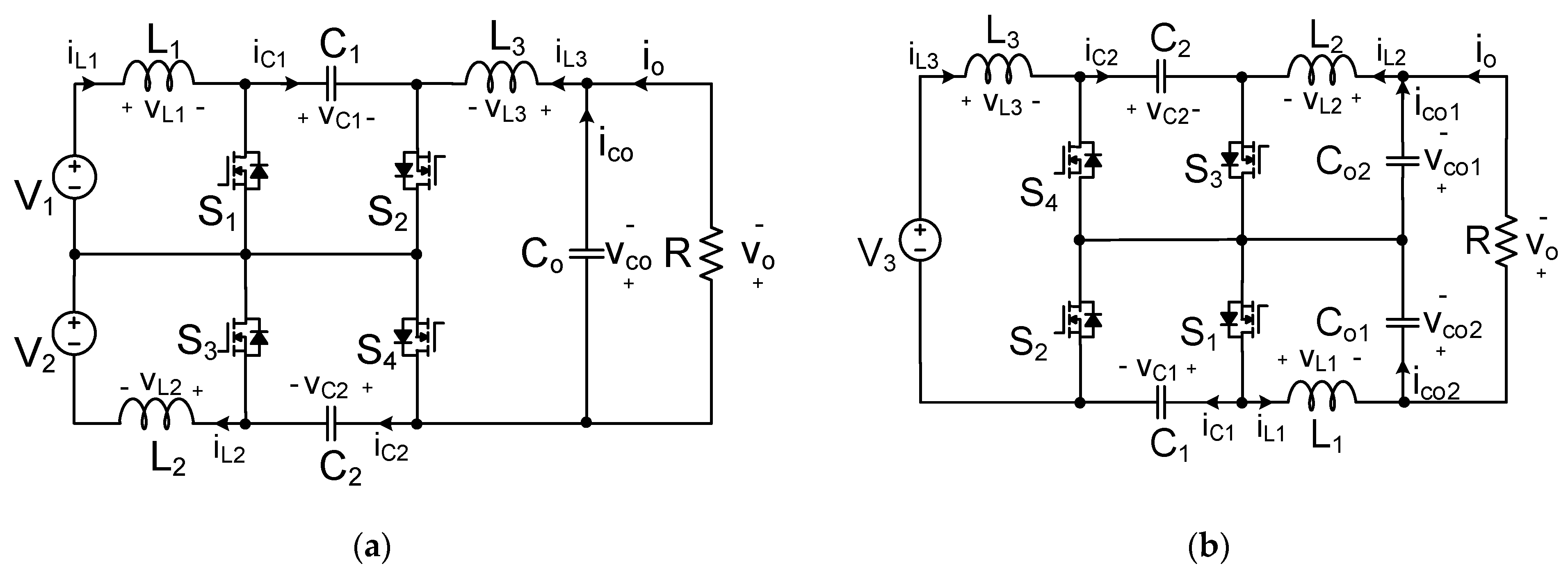
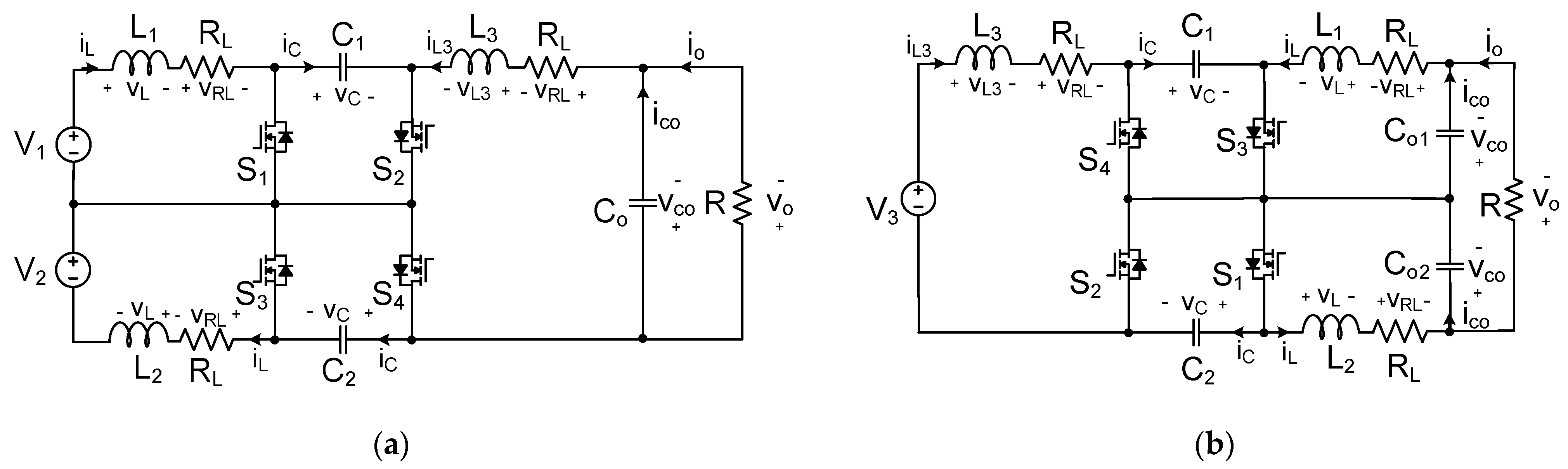
2. The Proposed DC–DC Bidirectional Converter Based on a Cuk Converter
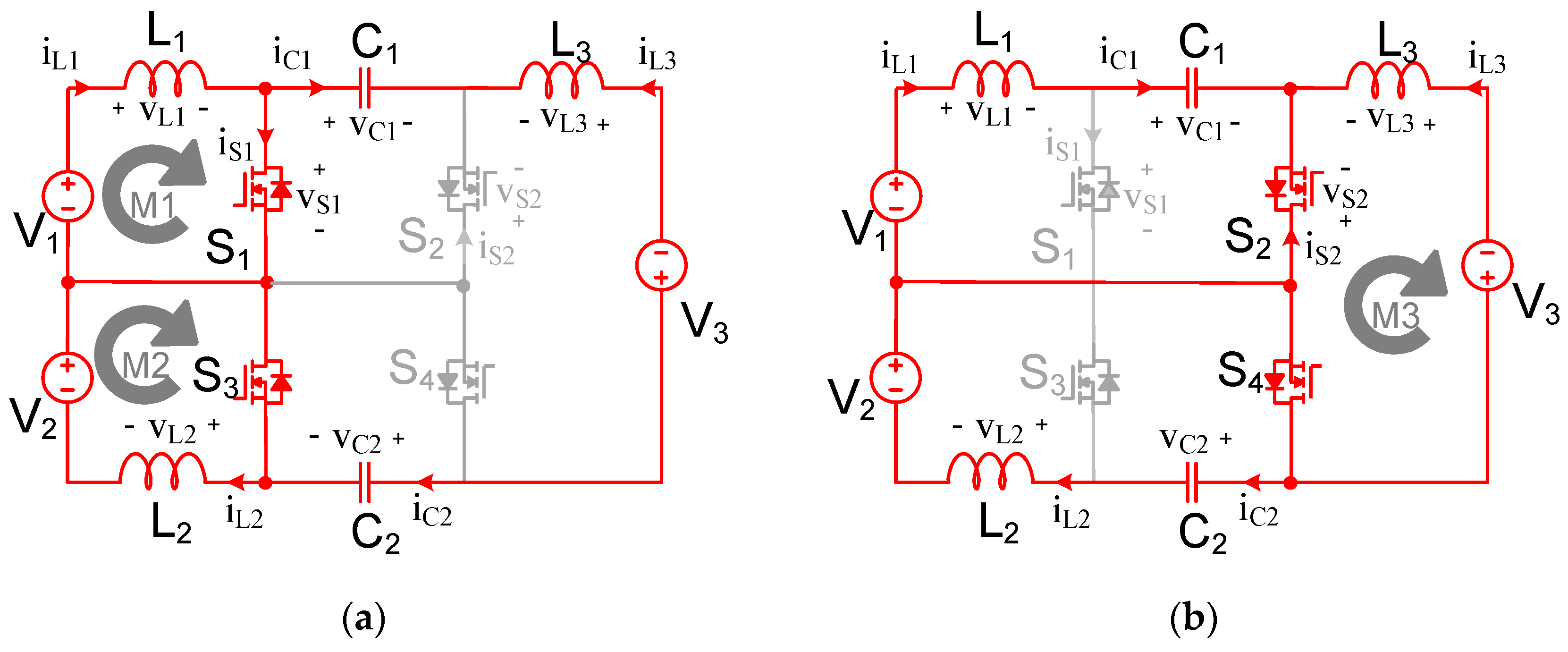
2.1. Operating Stages
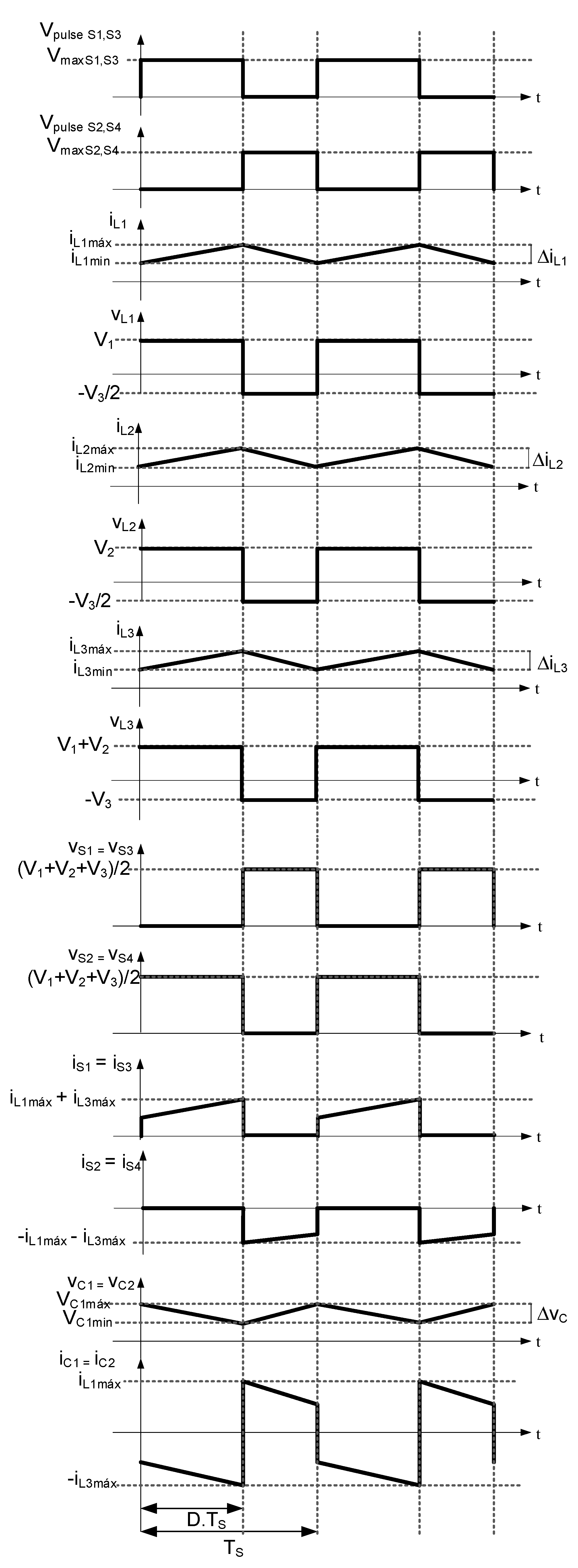
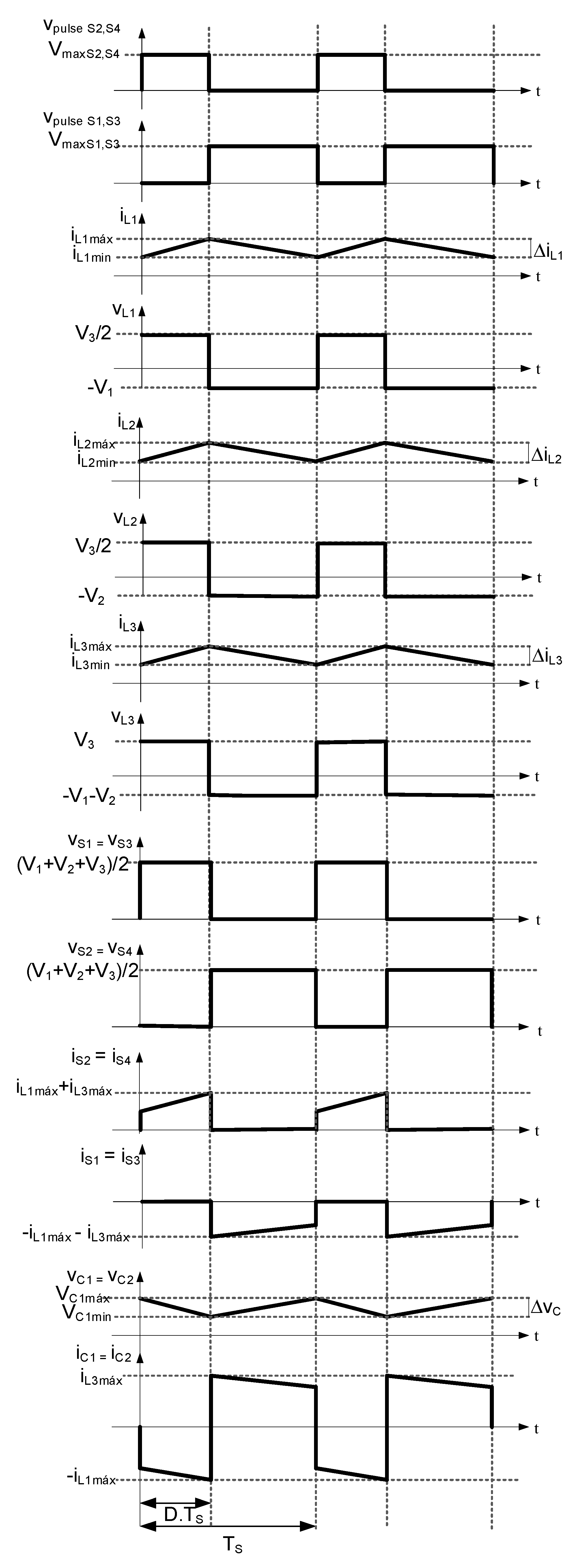
2.2. Main Ideal Waveforms
- -
- the currents in all inductors are composed of a continuous current with a high-frequency ripple;
- -
- the maximum voltage across the switches is equal to the sum of half of the input voltage and half of the output voltage;
- -
- the current of the switches is equal to the sum of the current in the inductors;
- -
- the voltage across the capacitors is equal to the sum of half of the input voltage and half of the output voltage.
2.3. Static Gain
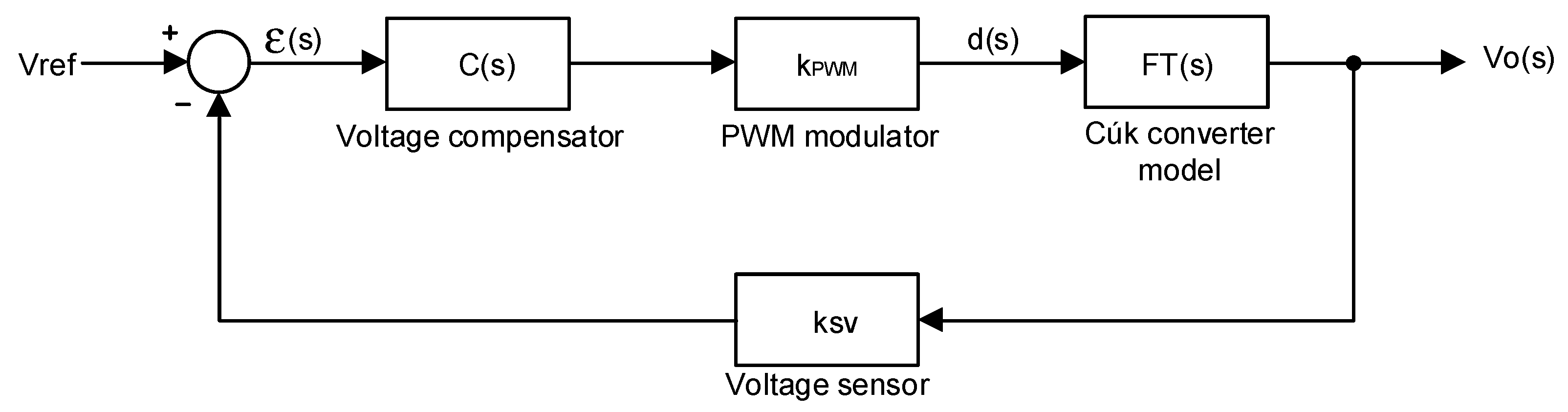
2.4. Control and PWM Scheme
2.5. Comparative Analysis
3. Control-Oriented Model for Voltage Control
3.1. Linearized Transfer Function in the Direct Mode without Losses
- A2 = 2.R.C1.L1.VC1
- A1 = −2.D.L1.(IL1 + IL3).R
- A0 = −2.R.VC1.(D − 1)
- B4 = R.C1.L1.L3.Co
- B3 = C1.L1.L3
- B2 = R.((2.(L1 + (1/2).L3)).Co.D2 − 2.Co.L3.D + C1.L1 + Co.L3)
- B1 = (2.L1 + L3).D2 − 2.L3.D + L3
- B0 = R.(D − 1)2
3.2. Linearized Transfer Function in the Reverse Mode without Losses
- A2 = 2.R.C1.L3.VC1
- A1 = −2.D.L3.(IL1 + IL3).R
- A0 = −4.R.VC1.(D − 1)
- B4 = R.C1.L1.L3.Co1
- B3 = 2.C1.L1.L3
- B2 = R.(((2.L1 + L3).D2 − 4.D.L1 + 2.L1).Co1 + C1.L3)
- B1 = (4.L1 + 2.L3).D2 − 8.D.L1 + 4.L1
- B0 = 2.R.(D − 1)2
3.3. Linearized Transfer Function in the Direct Mode with Losses
- A2 = 2.R.C1.L1.VC1
- A1 = −2.D.L1.(IL1 + IL3).R + 2.R.C1.VC1.RL
- A0 = 2.R.((−IL1 − IL3).RL − VC1).D + VC1)
- B4 = R.C1.L1.L3.Co
- B3 = (−IL1 − IL3).RL − VC1).D + VC1
- B2 = 2.Co.(L1 + (1/2).L3).R.D2 − 2.Co.D.L3.R + ((2.C1.RL + L3).Co + C1.L1).R + C1.(L1.RL + L3.RL)
- B1 = (3.Co.RL.R + 2.L1 + L3).D2 + (−2.Co.R.RL − 2.L3).D + (C1.RL + Co.RL).R + 2.C1.RL + L3
- B0 = (R + 3.RL).D2 + (−2.R − 2.RL).D + R + RL
3.4. Linearized Transfer Function in the Reverse Mode with Losses
- A2 = R.C1.L3.VC1
- A1 = R.(−L3.(IL1 + IL3).D + C1.VC1.RL)
- A0 = R.(((−IL1 − IL3).RL − 2.VC1).D + 2.VC1)
- B4 = R.C1.L1.L3.Co1
- B3 = (Co1.(L1.RL3 + L3.RL).R + 2.L1.L3).C1
- B2 = 2.R.Co1.(L1 + (1/2).L3).D2 − 4.Co1.D.L1.R + ((2.C1.RL + 2.L1).Co1 + C1.L3).R + 2.C1.(L1.RL + L3.RL)
- B1 = (3.Co1.RL.R + 4.L1 + 2.L3).D2 + (−4.Co1.R.RL − 8.L1).D + (C1.RL + 2.Co1.RL).R + 4.C1.RL + 4.L1
- B0 = (2.R + 6.RL).D2 + (−4.R − 8.RL).D + 2.R + 4.RL
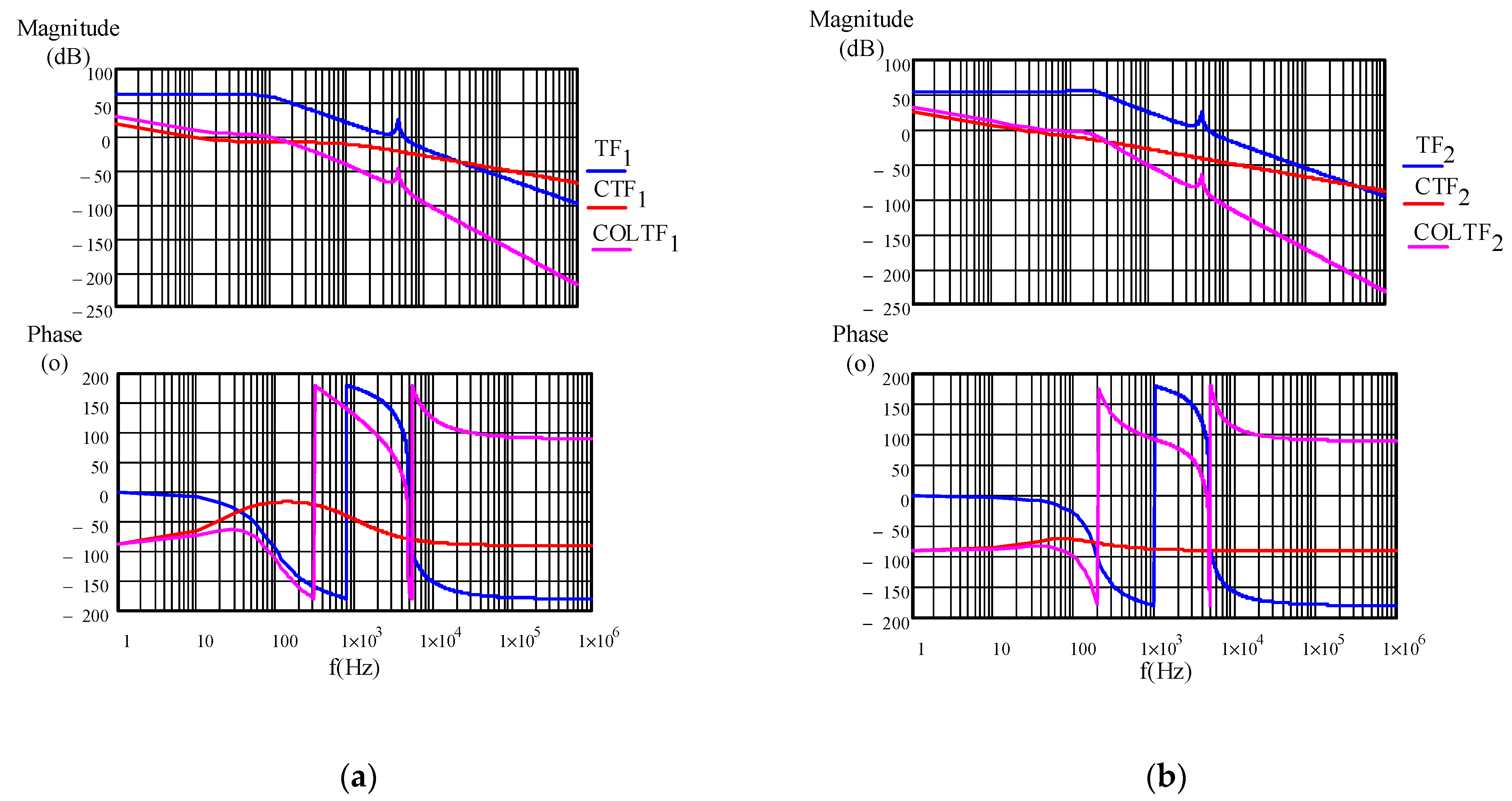
3.5. Validation of the Transfer Functions
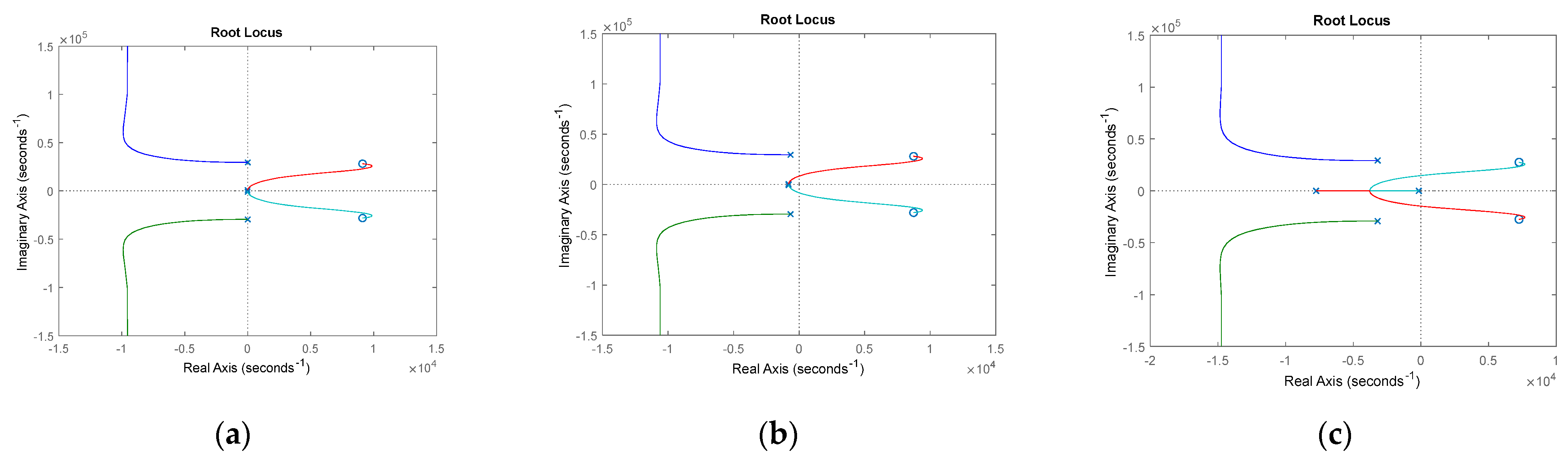
3.6. Root Locus Analysis
4. Compensator Design
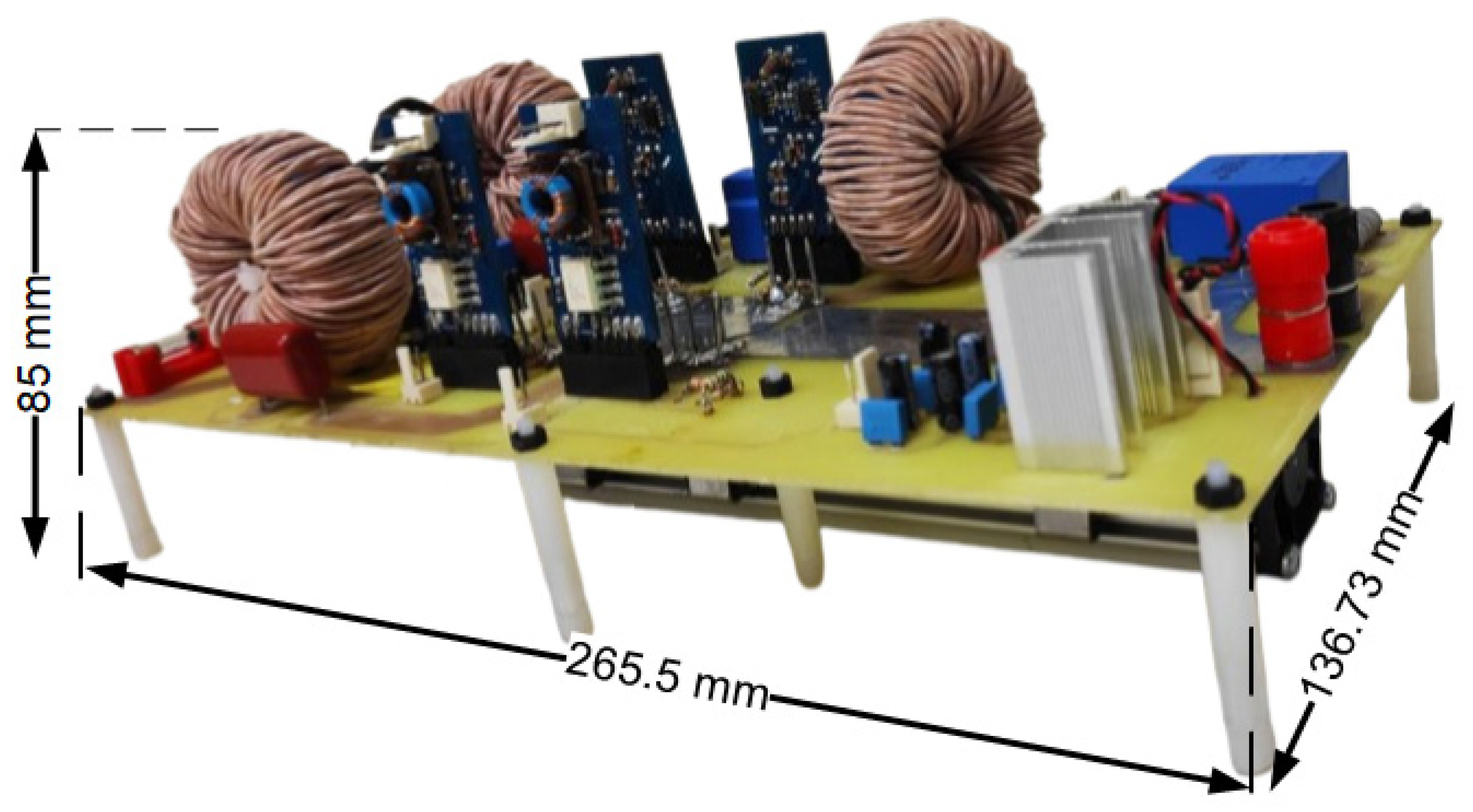
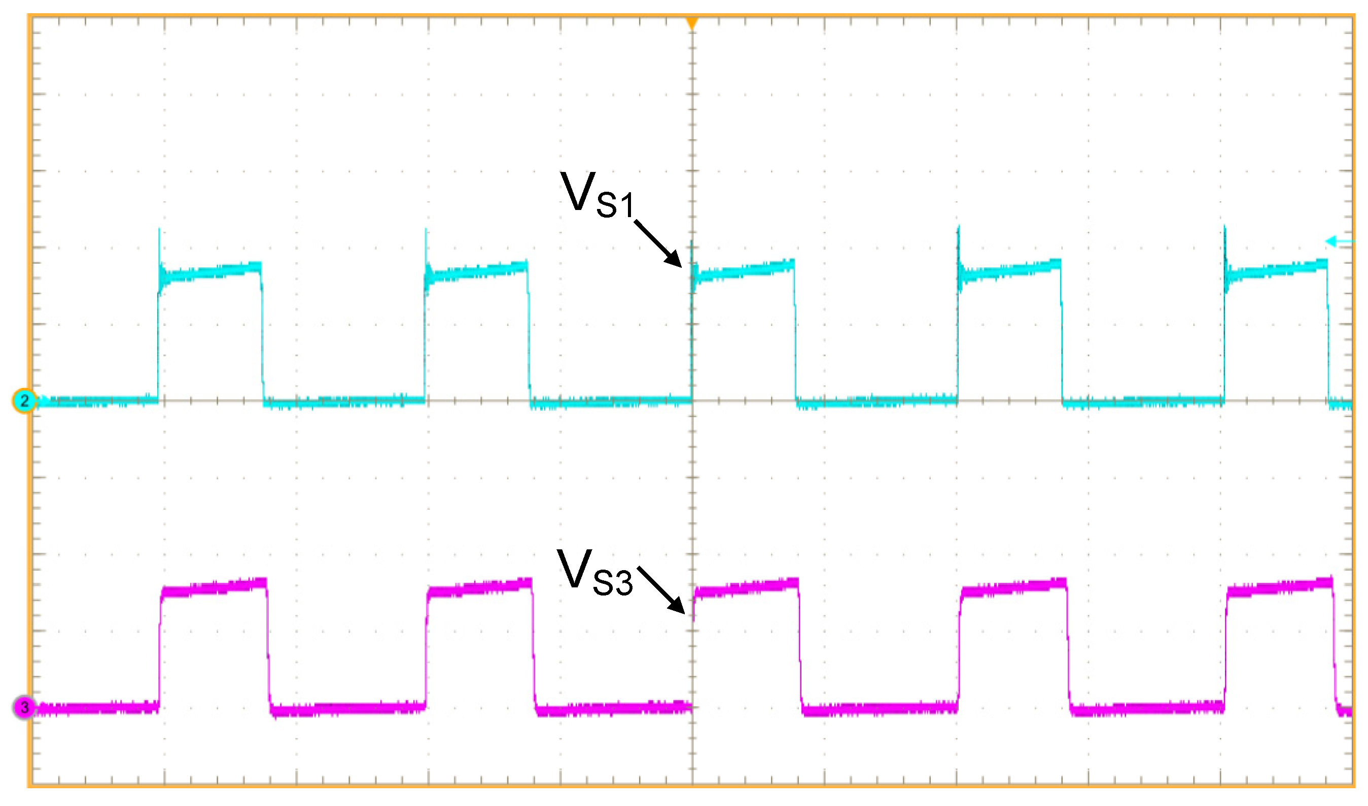
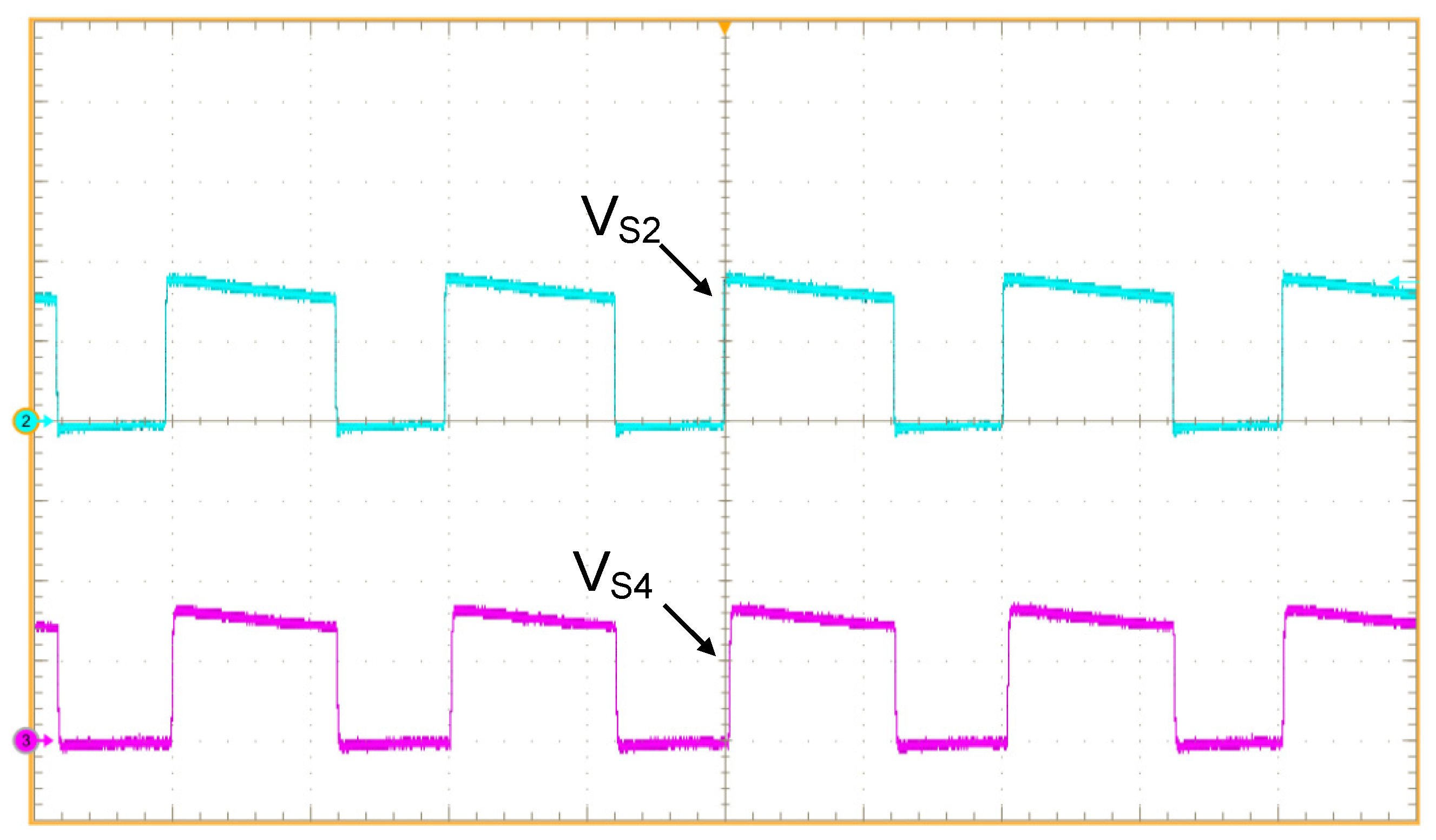
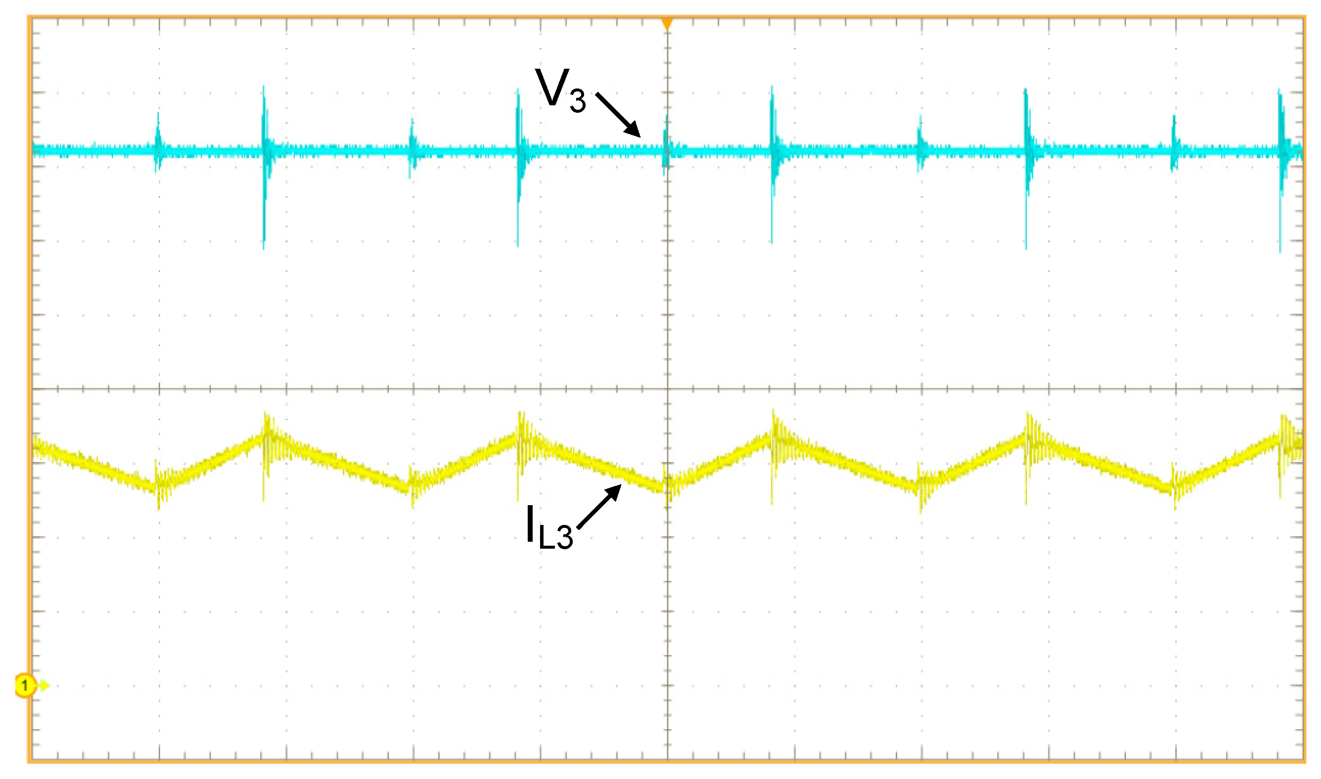
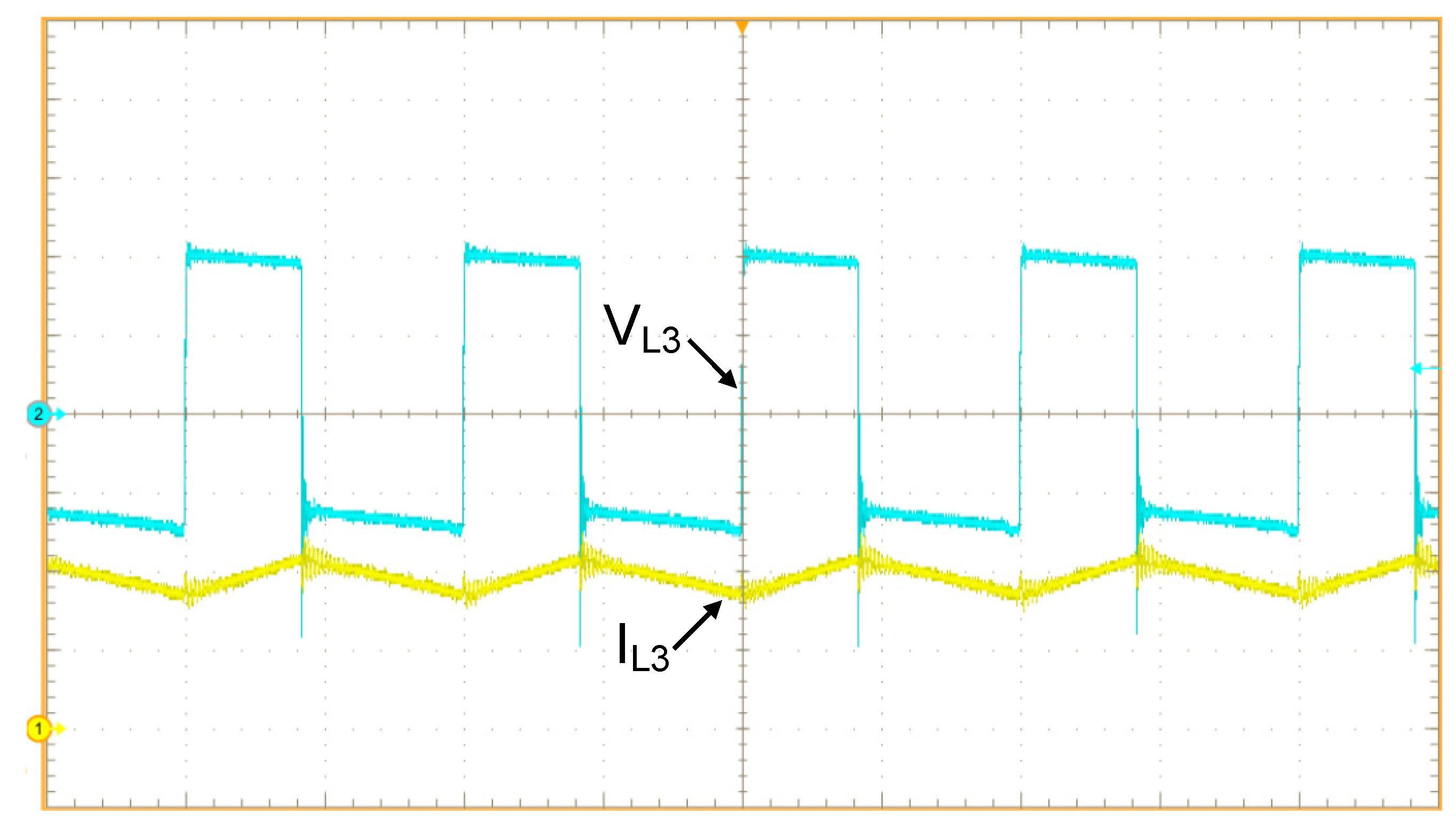
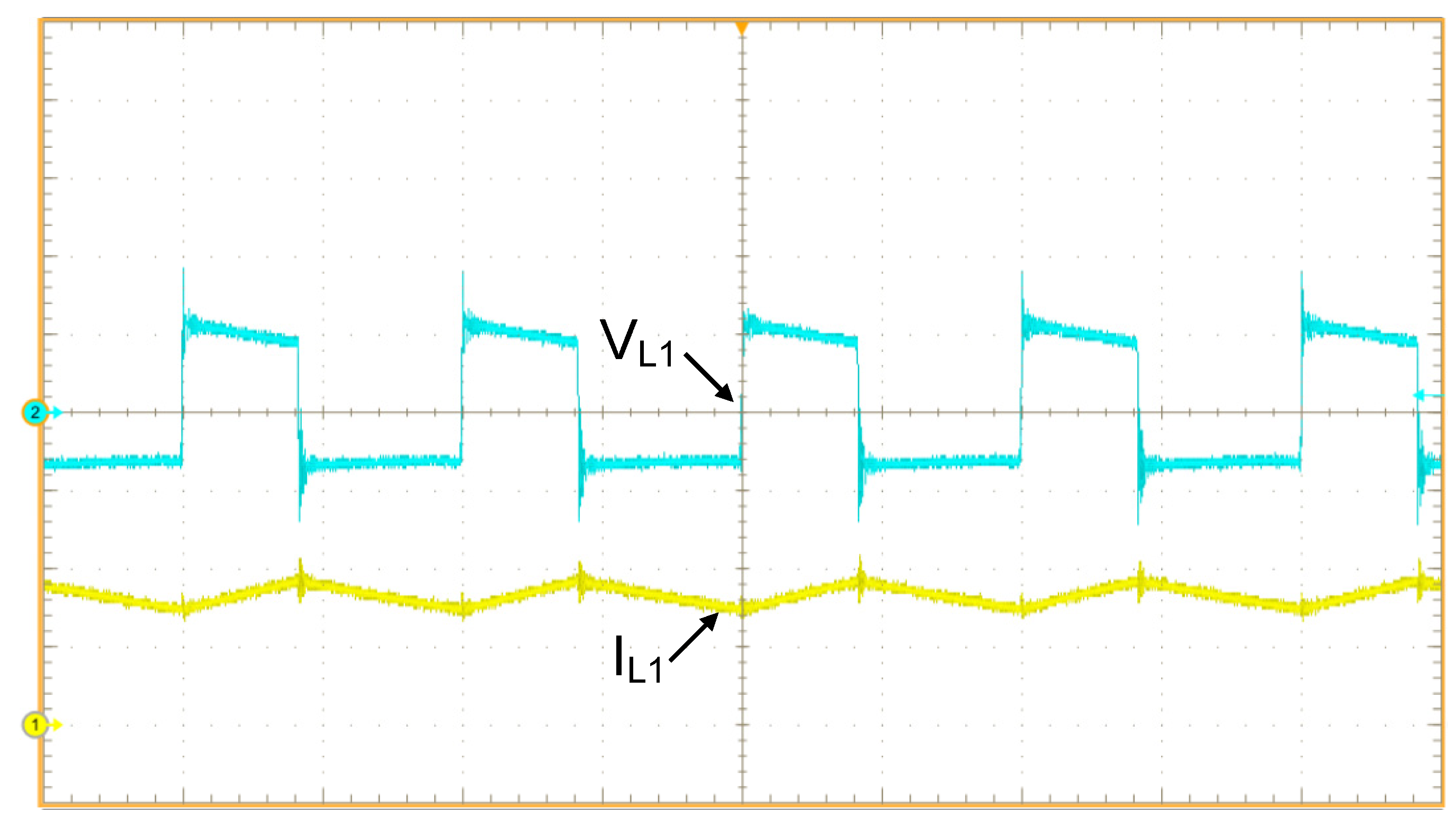
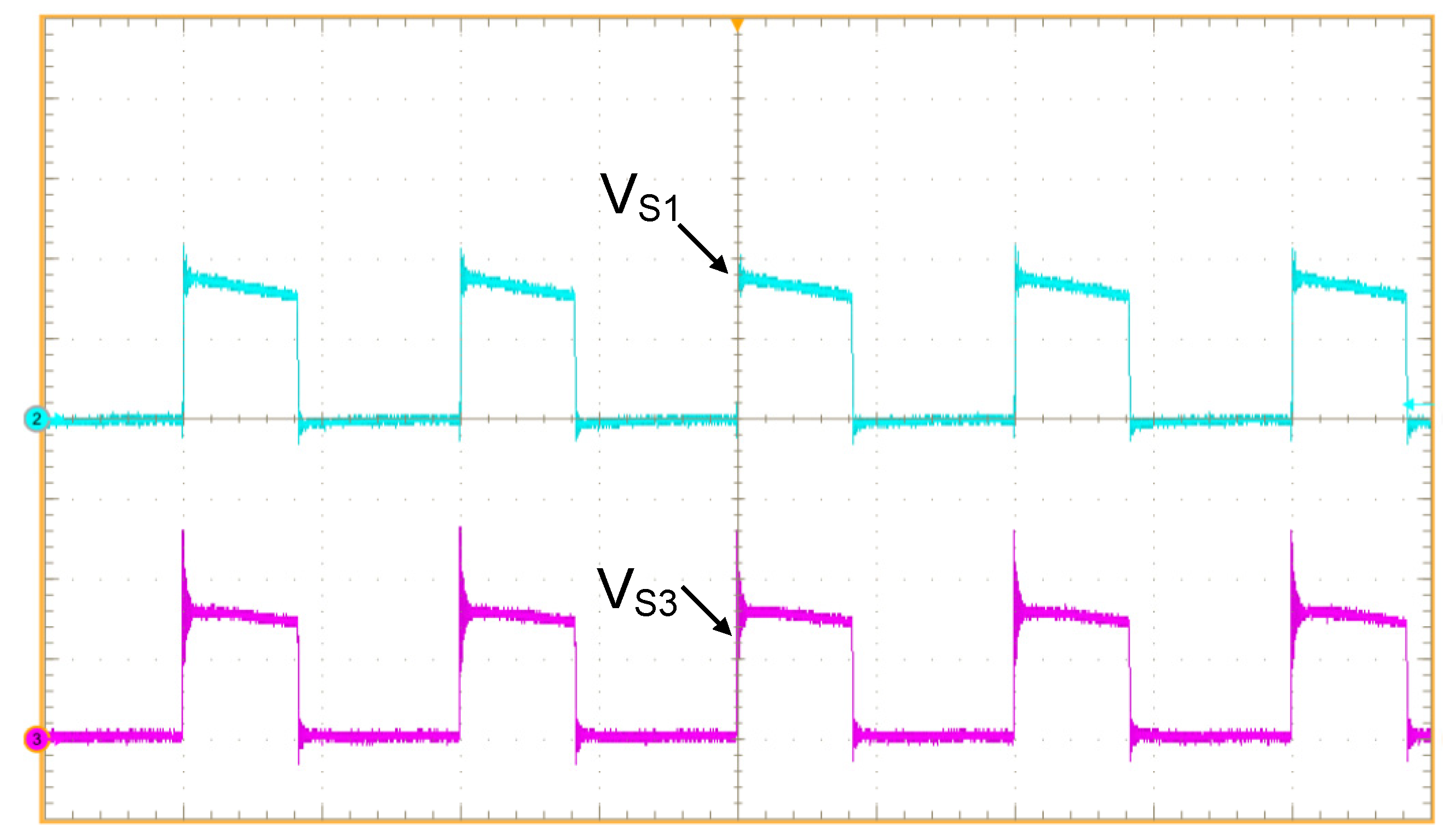
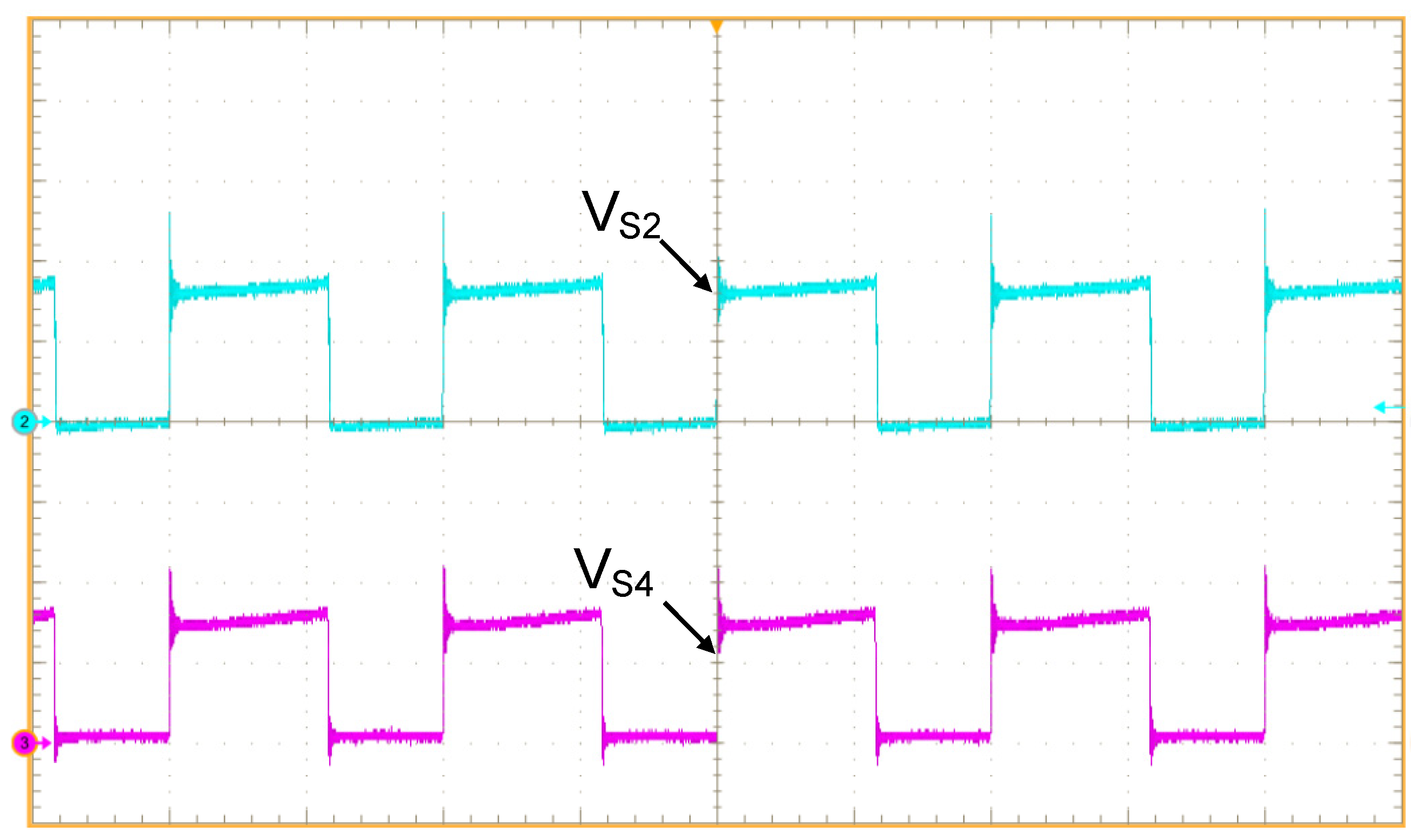
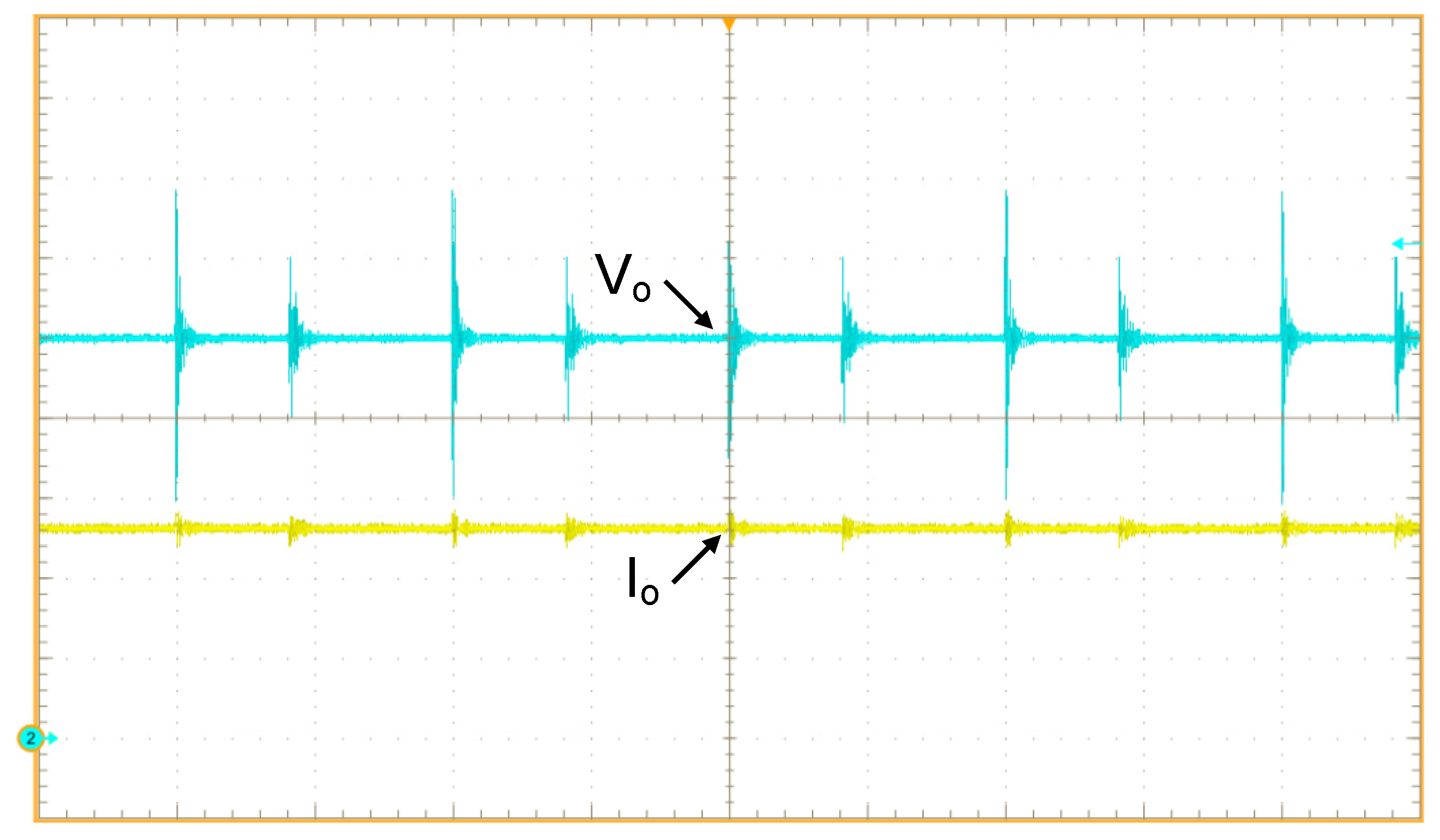
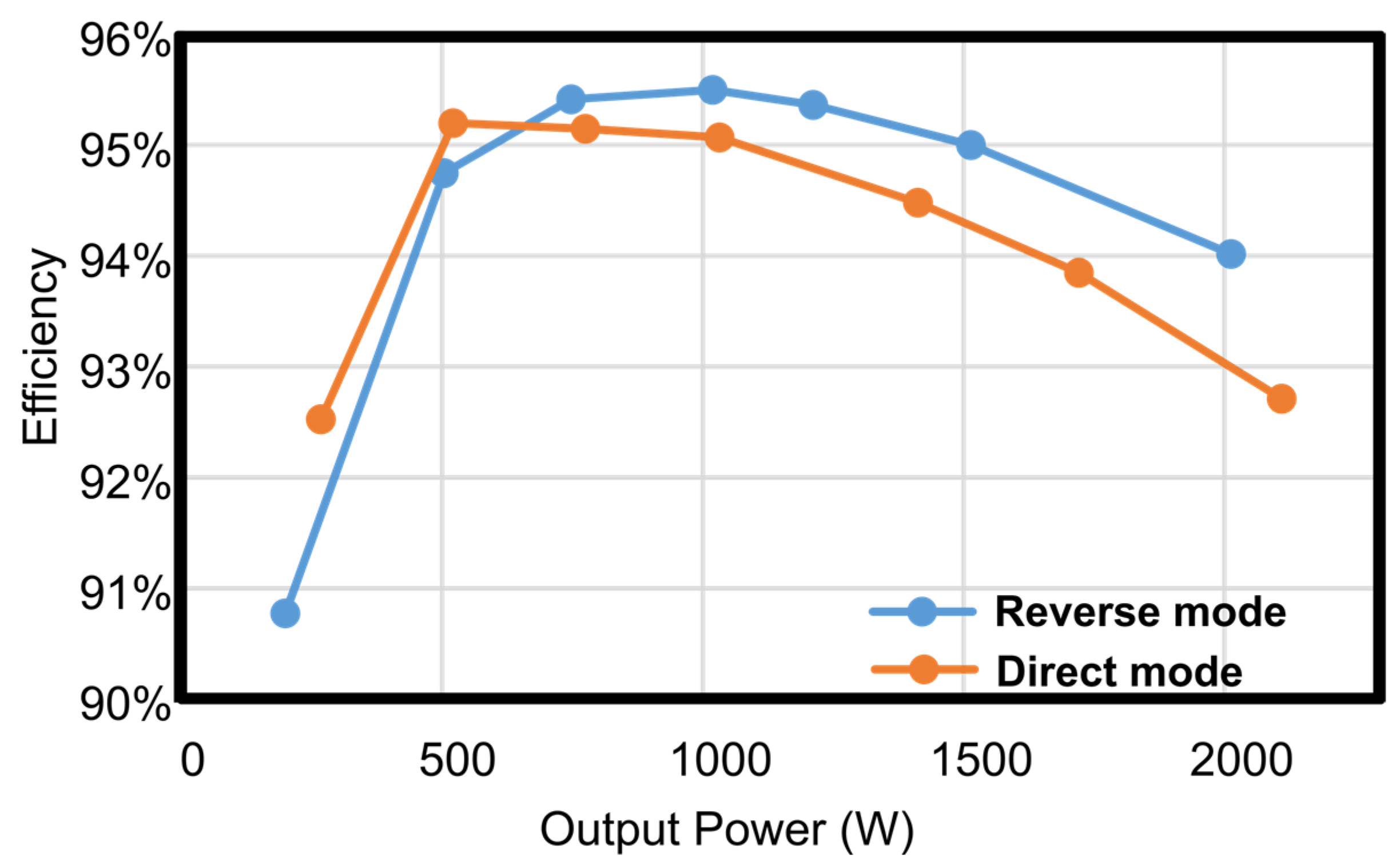
5. Experimental Results
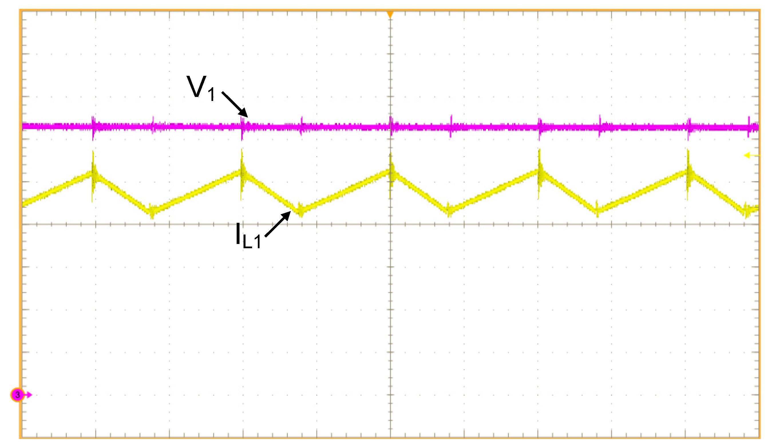
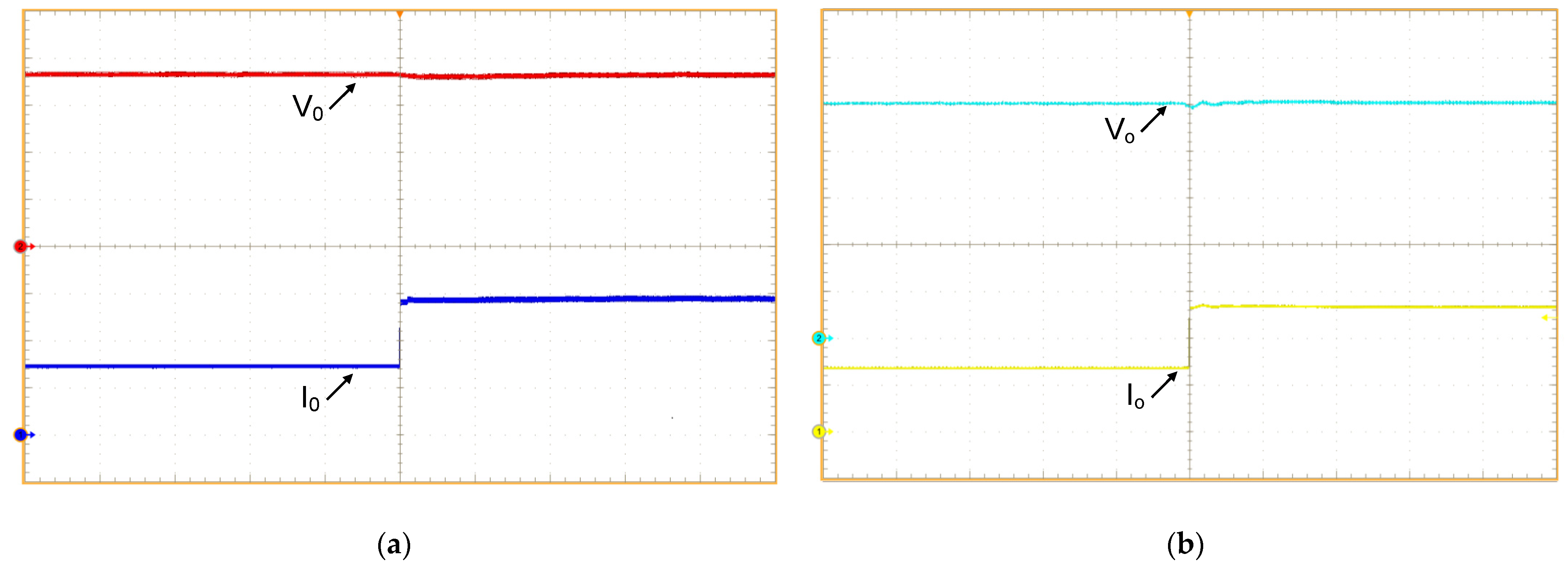
5.1. Waveforms Obtained in the Direct Mode with RC Load and Open Loop Operation
5.2. Waveforms Obtained in the Reverse Mode with RC Load and Open Loop Operation
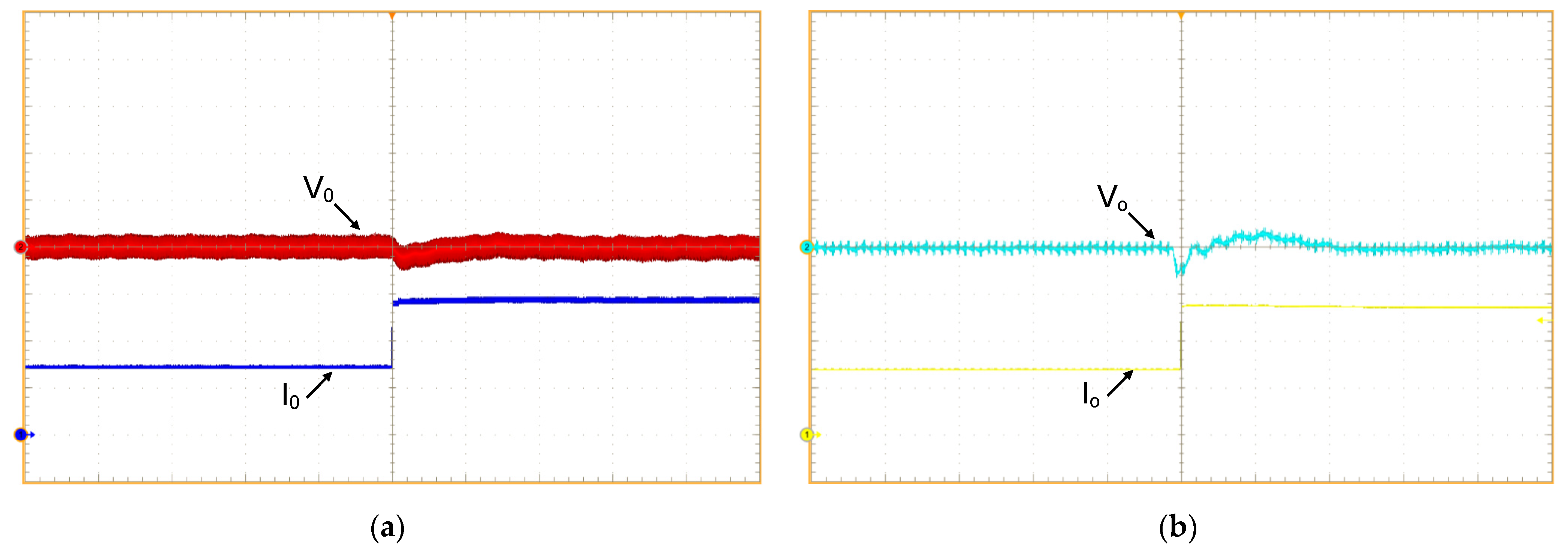
5.3. Waveforms Obtained with RC Load and Closed Loop Operation
6. Conclusions
Author Contributions
Funding
Data Availability Statement
Conflicts of Interest
References
- Dragičević, T.; Lu, X.; Vasquez, J.C.; Guerrero, J.M. DC microgrids—Part I: A review of control strategies and stabilization techniques. IEEE Trans. Power Electron. 2016, 31, 4876–4891. [Google Scholar] [CrossRef]
- Dragičević, T.; Lu, X.; Vasquez, J.C.; Guerrero, J.M. DC microgrids—Part II: A review of power architectures, applications, and standardization issues. IEEE Trans. Power Electron. 2016, 31, 3528–3549. [Google Scholar] [CrossRef]
- Rodriguez-Diaz, E.; Savaghebi, M.; Vasquez, J.C.; Guerrero, J.M. An overview of low voltage dc distribution systems for residential applications. In Proceedings of the IEEE 5th International Conference on Consumer Electronics, Berlin, Germany, 6–9 September 2015; pp. 318–322. [Google Scholar] [CrossRef]
- Elsayed, A.T.; Mohamed, A.A.; Mohammed, O.A. DC microgrids and distribution systems: An overview. Electr. Power Syst. Res. 2015, 119, 407–417. [Google Scholar] [CrossRef]
- Sofla, M.A.; Wang, L. Control of DC-DC bidirectional converters for interfacing batteries in microgrids. In Proceedings of the IEEE/PES Power Systems Conference and Exposition, Phoenix, AZ, USA, 20–23 March 2011; pp. 1–6. [Google Scholar] [CrossRef]
- Pires, V.F.; Pires, A.; Cordeiro, A. DC Microgrids: Benefits, Architectures, Perspectives and Challenges. Energies 2023, 16, 1217. [Google Scholar] [CrossRef]
- Gruner, V.F.; Zanotti, J.W.; Santos, W.M.; Pereira, T.A.; Schmitz, L.; Martins, D.C.; Coelho, R.F. Modified Current Sensorless Incremental Conductance Algorithm for Photovoltaic Systems. Energies 2023, 16, 790. [Google Scholar] [CrossRef]
- Al-Ismail, F.S. DC Microgrid Planning, Operation, and Control: A Comprehensive Review. IEEE Access 2021, 9, 36154–36172. [Google Scholar] [CrossRef]
- Ali, S.; Zheng, Z.; Aillerie, M.; Sawicki, J.-P.; Péra, M.-C.; Hissel, D. A Review of DC Microgrid Energy Management Systems Dedicated to Residential Applications. Energies 2021, 14, 4308. [Google Scholar] [CrossRef]
- Andrade, A.M.S.S.; da Silva Martins, M.L. Isolated boost converter based high step-up topologies for PV microinverter applications. IET Power Electron. 2020, 13, 1353–1363. [Google Scholar] [CrossRef]
- Broday, G.R.; Lopes, L.A. A novel 5-Switch tapped-inductor multi-state bidirectional DC-DC converter. In Proceedings of the IEEE International Conference on Industrial Technology (ICIT), Lyon, France, 20–22 February 2018; pp. 596–599. [Google Scholar] [CrossRef]
- Tibola, G.; Duarte, J.L. Isolated bidirectional DC-DC converter for interfacing local storage in two-phase DC grids. In Proceedings of the IEEE 8th International Symposium on Power Electronics for Distributed Generation Systems (PEDG), Florianopolis, Brazil, 17–20 April 2017; pp. 1–8. [Google Scholar] [CrossRef]
- Lenz, E.; Pagano, D.J.; Saito, M.T.; Pou, J. Nonlinear Control of a Bidirectional Power Converter for Connecting Batteries in DC Microgrids. In Proceedings of the IEEE 8th International Symposium on Power Electronics for Distributed Generation Systems (PEDG), Florianopolis, Brazil, 17–20 April 2017; pp. 1–8. [Google Scholar] [CrossRef]
- Soman, D.E.; Vikram, K.; Krishna, R.; Gabrysch, M.; Kottayil, S.K.; Leijon, M. Analysis of three-level Buck-Boost converter operation for improved renewable energy conversion and smart grid integration. In Proceedings of the IEEE International Energy Conference (ENERGYCON), Cavtat, Croatia, 13–16 May 2014; pp. 76–81. [Google Scholar] [CrossRef]
- Elamalayil Soman, D.; Leijon, M. Cross-Regulation assessment of DIDO Buck-Boost converter for renewable energy application. Energies 2017, 10, 846. [Google Scholar] [CrossRef]
- Park, C.H.; Jang, S.J.; Lee, B.K.; Won, C.Y.; Lee, H.M. Design and control algorithm research of active regenerative bidirectional DC/DC converter used in electric railway. In Proceedings of the 7th International Conference on Power Electronics, Daegu, Republic of Korea, 22–26 October 2007; pp. 790–794. [Google Scholar] [CrossRef]
- Pham, C.; Kerekes, T.; Teodorescu, R. High efficient bidirectional battery converter for residential PV systems. In Proceedings of the 3rd IEEE International Symposium on Power Electronics for Distributed Generation Systems (PEDG), Aalborg, Denmark, 25–28 June 2012; pp. 890–894. [Google Scholar] [CrossRef]
- Uddin, K.; Moore, A.D.; Barai, A.; Marco, J. The effects of high frequency current ripple on electric vehicle battery performance. Appl. Energy 2016, 178, 142–154. [Google Scholar] [CrossRef]
- Middlebrook, R.D.; Cuk, S.; Behen, W. A new battery charger/discharger converter. In Proceedings of the IEEE Power Electronics Specialists Conference (PESC), Syracuse, NY, USA, 13–15 June 1978; pp. 251–255. [Google Scholar]
- De Almeida, A.B.; Font, C.H.I. DC-DC Bidirectional 4-Switch Cúk Converter with Voltage-Doubler Concept for Interfacing Batteries in Microgrids. In Proceedings of the 2018 13th IEEE International Conference on Industry Applications (INDUSCON), Sao Paulo, Brazil, 12–14 November 2018; pp. 263–268. [Google Scholar]
- Agarwal, A.; Singh, R.K. Implementation and Control of a Magnetically Coupled ‘Cuk Converter with Damping Network for Optimal Battery Charging’. In Proceedings of the 7th IET International Conference on Power Electronics, Machines and Drives (PEMD 2014), Manchester, UK, 8–10 April 2014; pp. 1–12. [Google Scholar]
- Chinmaya, K.A.; Singh, G.K. A Plug-in Electric Vehicle (PEV) with Compact Bidirectional Cuk Converter and Sturdier Induction Motor Drive. In Proceedings of the IECON 2018-44th Annual Conference of the IEEE Industrial Electronics Society, Washington, DC, USA, 21–23 October 2018; pp. 937–942. [Google Scholar]
- Khaleghi, H.; Varjani, A.Y.; Mohamadian, M. A new bidirectional zeta DC/DC converter. In Proceedings of the 5th Annual International Power Electronics, Drive Systems and Technologies Conference (PEDSTC 2014), Tehran, Iran, 5–6 February 2014; pp. 131–136. [Google Scholar]
- Shahin, M. Analysis of bidirectional SEPIC/Zeta converter with coupled inductor. In Proceedings of the 2015 International Conference on Technological Advancements in Power and Energy (TAP Energy), Kollam, India, 24–26 June 2015; pp. 103–108. [Google Scholar]
- Lee, H.Y.; Liang, T.J.; Chen, J.F.; Chen, K.H. Design and implementation of a bidirectional SEPIC-Zeta DC-DC Converter. In Proceedings of the 2014 IEEE International Symposium on Circuits and Systems (ISCAS), Melbourne, VIC, Australia, 1–5 June 2014; pp. 101–104. [Google Scholar]
- Kim, I.D.; Paeng, S.H.; Ahn, J.W.; Nho, E.C.; Ko, J.S. New bidirectional ZVS PWM sepic/zeta DC-DC converter. In Proceedings of the 2007 IEEE International Symposium on Industrial Electronics, Vigo, Spain, 4–7 June 2007; pp. 555–560. [Google Scholar]
- de Sá, M.V.D.; Andersen, R.L. Dynamic modeling and design of a Ćuk converter applied to energy storage systems. In Proceedings of the IEEE 13th Brazilian Power Electronics Conference and 1st Southern Power Electronics Conference (COBEP/SPEC), Fortaleza, Brazil, 29 November–2 December 2015; pp. 1–6. [Google Scholar]
- Faistel, T.M.K.; Font, C.H.I.; Andrade, A.M.S.S.; da Silva Martins, M.L. Modelling and control of DC–DC Ćuk converter with R2P2 and voltage multiplier cells for PV applications. IET Power Electron. 2019, 12, 2214–2223. [Google Scholar] [CrossRef]
- Dixon, L.H., Jr. The Right-Half-Plane Zero—A Simplified Explanation; Technical Note; Literature Number SLUP084; Texas Instrument: Dallas, TX, USA, 2017. [Google Scholar]
- Leoncini, M.; Levantino, S.; Ghioni, M. Design issues and performance analysis of CCM boost converters with RHP zero mitigation via inductor current sensing. J. Power Electron. 2021, 21, 285–295. [Google Scholar] [CrossRef]


| Characteristic | Conventional Cuk | Voltage-Doubler Cuk |
|---|---|---|
| Component count | 5 | 9 |
| Number of inductors | 2 | 3 |
| Number of capacitors | 1 | 2 |
| Number of switches | 2 | 4 |
| Input characteristic | Current source | Current source |
| Output characteristic | Current source | Current source |
| Static characteristic | Step down/Step up | Step down/Step up |
| Static gain | ||
| Voltage stress on capacitors | ||
| Voltage stress on switches |
| Specifications | Value |
|---|---|
| Average value of voltage sources V1 and V2 | 125 V |
| Average value of voltage source V3 | 360 V |
| Output rated power (Po) | 2000 W |
| Switching frequency (fs) | 100 kHz |
| Voltage ripple in capacitors C1 and C2 (VC1,2) | 10% |
| Voltage ripple in capacitors Co, Co1, and Co2 (VCo) | 1% |
| Current ripple in inductors L1, L2, and L3 (iL1,2,3) | 20% |
| Parameters | Value |
|---|---|
| Equivalent load resistance (R)—direct mode | 64.80 Ω |
| Equivalent load resistance (R)—reverse mode | 31.25 Ω |
| Capacitive bank (Co)—direct mode | 1410.0 μF |
| Capacitive bank (Co1) and (Co2)—reverse mode | 1410.0 μF |
| Capacitors (C1) and (C2) | 1.0 μF |
| Inductors (L1) and (L2) | 461.07 μF |
| Inductor (L3) | 1.33 mH |
| Inductor resistances (RL) | 1 Ω |
| Average current of inductors L1 (IL1) and L2 (IL2) | 8.0 A |
| Average current of inductor L3 (IL3) | 5.56 A |
| Average voltage in capacitors C1 (VC1) and C2 (VC2) | 305.0 V |
| Nominal duty cycle (D)—direct mode | 0.59 |
| Nominal duty cycle (D)—reverse mode | 0.41 |
| Parameters | Direct Mode | Reverse Mode |
|---|---|---|
| Vref | 2.5 V | 2.5 V |
| ks | 0.00694 | 0.01 |
| Vpk | 3.5 V | 3.5 V |
| KPWM | 0.37 | 0.37 |
| fc | 100 Hz | 50 Hz |
| fz | 20 Hz | 50 Hz |
| fp | 1 kHz | 100 Hz |
| kC | 2615 | 254.47 |
| Components | Specification |
|---|---|
| Inductors L1 and L2 | Inductance: 474 μF Number of turns: 57 Wire: 64 × 32 AWG Core: 0088439A7 AmoFlux |
| Inductor L3 | Inductance: 1.35 mF Number of turns: 97 Wire: 32 × 32 AWG Core: 0088439A7 AmoFlux |
| Capacitors C1 and C2 | 1 μF/630 V |
| Switches S1, S2, S3, and S4 | SCT3080AL (650 V/30 A/80 mΩ) |
| Heatsink | LAM3K15012 |
Disclaimer/Publisher’s Note: The statements, opinions and data contained in all publications are solely those of the individual author(s) and contributor(s) and not of MDPI and/or the editor(s). MDPI and/or the editor(s) disclaim responsibility for any injury to people or property resulting from any ideas, methods, instructions or products referred to in the content. |
© 2024 by the authors. Licensee MDPI, Basel, Switzerland. This article is an open access article distributed under the terms and conditions of the Creative Commons Attribution (CC BY) license (https://creativecommons.org/licenses/by/4.0/).
Share and Cite
Lopes, W.F.; Martins, M.L.d.S.; Converti, A.; Siqueira, H.V.; Illa Font, C.H. Experimental Evaluation of a 2 kW/100 kHz DC–DC Bidirectional Converter Based on a Cuk Converter Using a Voltage-Doubler Concept. Energies 2024, 17, 362. https://doi.org/10.3390/en17020362
Lopes WF, Martins MLdS, Converti A, Siqueira HV, Illa Font CH. Experimental Evaluation of a 2 kW/100 kHz DC–DC Bidirectional Converter Based on a Cuk Converter Using a Voltage-Doubler Concept. Energies. 2024; 17(2):362. https://doi.org/10.3390/en17020362
Chicago/Turabian StyleLopes, Wanderson Francisco, Mário Lúcio da Silva Martins, Attilio Converti, Hugo Valadares Siqueira, and Carlos Henrique Illa Font. 2024. "Experimental Evaluation of a 2 kW/100 kHz DC–DC Bidirectional Converter Based on a Cuk Converter Using a Voltage-Doubler Concept" Energies 17, no. 2: 362. https://doi.org/10.3390/en17020362