Article

Novel Burst-Mode Control for Medium-to-Light Load Operation of Dual-Active-Bridge Converters, Achieving Minimum Backflow Power, Zero-Voltage-Switching, and DC Bias Suppression

by
Chanh-Tin Truong
,
Byeong-Ryeol Na
,
Jeong-Soo Park
and
Sung-Jin Choi
*
Department of Electrical, Electronic and Computer Engineering, University of Ulsan, Ulsan 44610, Republic of Korea
*
Author to whom correspondence should be addressed.
Energies 2024, 17(22), 5748; https://doi.org/10.3390/en17225748
Submission received: 24 October 2024 / Revised: 8 November 2024 / Accepted: 14 November 2024 / Published: 17 November 2024
(This article belongs to the Section F3: Power Electronics)

Abstract

:
The dual-active-bridge (DAB) converter is widely used in many applications such as solid-state transformers, multi-port converters, and on-board chargers. Nevertheless, its efficiency degrades significantly under light-load conditions due to high switching and conduction losses. Since a detailed analysis for burst-mode design has not been presented in the literature, effective burst-mode control for the light-load condition is proposed in this paper. In the proposed burst-mode, the regular duty cycle and the burst duty cycle are optimally coordinated to achieve the zero-voltage-switching (ZVS) condition and the minimum backflow power at the same time. Moreover, DC bias current is effectively eliminated in the proposed burst-mode. The switching loss and conduction loss are simultaneously minimized in the proposed burst-mode control. Therefore, the light-load efficiency is significantly improved. The detailed analysis and design procedure are also presented for both buck- and boost-mode operations to deal with widely varying output voltage ranges. The control mode switching condition is determined for achieving the ZVS condition for the whole load condition; thus, the proposed burst-mode control flowchart is presented. A 4 kW DAB converter prototype is built to verify the proposed method and the experiment results show about a 2% increment in efficiency of the proposed method compared to the conventional burst-mode method.

1. Introduction

The isolated dual-active-bridge (DAB) converter is one of the most popular converters in applications such as solid-state transformers, multi-port converters, and other applications due to its bidirectional and symmetrical structure, zero-voltage-switching (ZVS), and wide voltage gain regulation capabilities [1,2,3]. These features allow it to be used in systems such as energy storage systems and uninterruptible power supplies, which are characterized by widely varying output voltage conditions from renewable energy sources or loads such as energy storages that include batteries and variable loads. These characteristics of the DAB converter necessitate high efficiency over a wide range of effective input/output voltage ratios, particularly under light-load conditions.
The single-phase-shift (SPS) control for DAB converters is the most popular modulation method for DAB control strategies used by industrial practitioners due to its low cost, simple implementation, and easy design [4]. However, SPS control of DAB increases backflow power under light-loads, generating circulating currents [5,6,7,8]. To overcome this limitation, many modulation controls such as extended-phase-shift (EPS), dual-phase-shift (DPS), and triple-phase-shift (TPS) have been proposed [9,10,11,12,13]. However, the complexity of control strategies with many control variables make optimal control difficult [14]. Furthermore, if the voltage gain is not unity in light-load conditions, hard switching occurs, resulting in reduced efficiency [15,16]. Although the magnetizing inductance of a transformer is utilized by introducing an air gap to achieve a full-range ZVS and improve the light-load efficiency of the DAB converter [4], this is not recommended due to the increased size, cost, and losses [17,18,19].
To address the two main issues of SPS control under a light-load operation of the DAB, burst-mode is widely used. Burst-mode significantly reduces conduction loss, switching loss, and core loss [20], and has been widely used in power converters [21,22,23]. In burst-mode control, the switching cycles are minimized during light-load conditions, which significantly improves efficiency. This is in contrast to EPS, DPS, and TPS, which continuously adjust phase shifts and maintain high switching losses, leading to a significant improvement in the light-load efficiency of the burst-mode control, particularly in applications with highly variable load conditions. Recently, burst-mode has been applied to DAB converters to improve light-load efficiency [24]. The design of burst-mode parameters, such as the burst-mode frequency and burst-mode duty cycle, are presented in [25]. Small-signal modeling for burst-mode control is presented in [26]. However, DC bias occurs in a conventional burst-mode at every first cycle of a burst-mode operation, which can cause current spikes in the inductor and an oversaturation of the transformer [27,28,29]. In conventional method, the current direction is considered for deriving the ZVS condition. However, the positive or negative direction of the current does not always guarantee soft switching in MOSFETs [30,31]. To further elaborate the ZVS condition, the energy in the output capacitors of the MOSFETs in the full-bridge should be considered as well [30,31]. Moreover, the regular duty cycle and the burst duty cycle are not optimally coordinated to achieve the zero-voltage-switching (ZVS) condition and the minimum backflow power at the same time. Therefore, the switching loss and conduction loss are not simultaneously minimized; thus, the light-load efficiency is not much improved.
To improve the performance of the burst-mode, the optimal burst-mode control for the light-load condition is proposed in this paper. In the proposed method, the optimal duty cycle is adaptively calculated in the burst-mode control to minimize the backflow power, while the burst duty cycle is used for regulating the output voltage. Moreover, the DC bias current is effectively eliminated in the proposed burst-mode. This paper is an expanded version of our conference paper, which was presented only for buck-mode operations [32]. In this paper, a detailed analysis and design procedure are presented for both buck- and boost-mode operations to deal with widely varying output voltage range. The control mode switching condition is determined for achieving the ZVS condition for whole-load conditions, and thus, the proposed burst-mode control flowchart is presented, which is newly appended. Moreover, the MOSFETs’ nonlinear output capacitance characteristics are taken into account for the complete ZVS condition. The advantages of the proposed burst-mode can be listed as follows:
  • No additional components are needed for efficiency improvement under light-load conditions.
  • Complete ZVS condition is considered for optimal operation of burst-mode and ZVS is achieved for entire load range.
  • Backflow power is minimized at the light-load condition.
  • DC bias current elimination is applied for the burst-mode.
  • A mode switching algorithm between the burst-mode and normal-mode is proposed.
A comparative table of advantages and disadvantages of the proposed method compared with other investigations is shown in Table 1.
The rest of this paper is structured as follows: Section 2 discusses the operation of the DAB converter, then Section 3 presents the proposed burst-mode for the DAB converter. The design procedure and control mode sequence are presented in Section 4 and Section 5, respectively. The analysis is verified via experimentation in Section 6. Finally, the results of the study are summarized in Section 7.

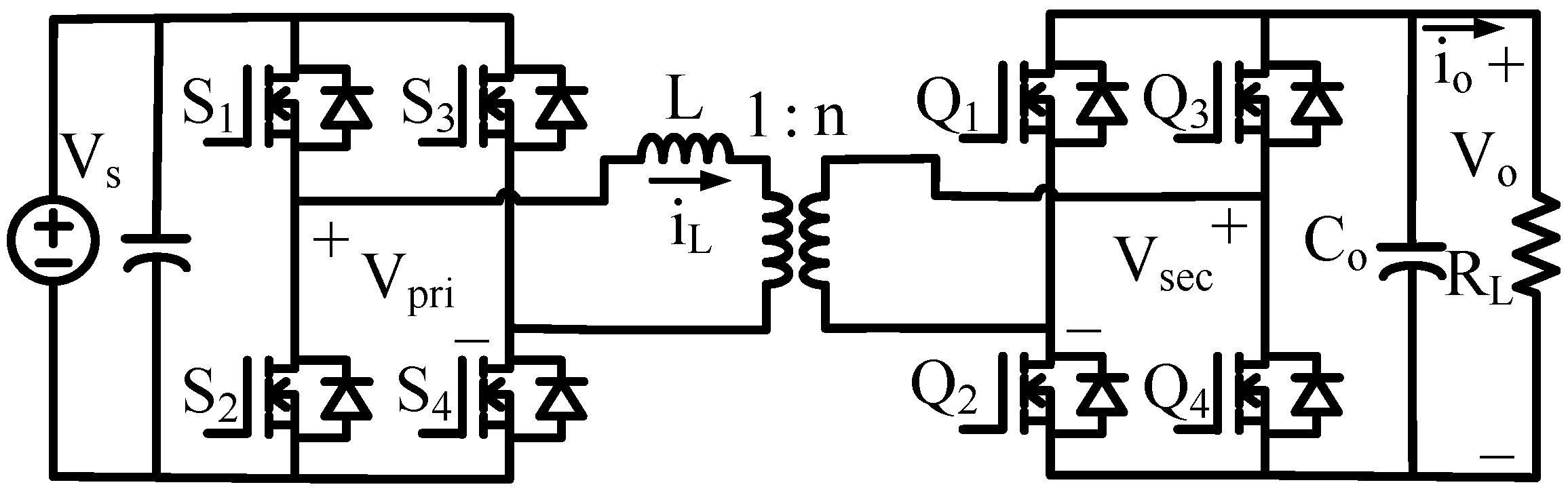
2. Operation of the Isolated DAB Converter

Figure 1 shows a DAB converter circuit that has two active full bridges to generate a square wave voltage; a series inductor L to store energy for power transfer; and a transformer with a turn ratio of 1:n to meet the high-voltage ratio and provide galvanic isolation. The key waveforms under the SPS modulation of the DAB converter in either buck or boost operation modes are shown in Figure 2, where the currents at the vertices are given by
I 0 = V s 2 D 1 + V o n T s 4 L I 1 = V s + V o n 2 D 1 T s 4 L .
According to the analysis in [6,15], the voltage gain M and the output power P o of the DAB converter are given by
M = V o n V s = D ( 1 D ) T s R L 2 L n 2 ,
P o = V s V o D ( 1 D ) 2 n f s L
where D, T s , and R L are the regular duty cycle, the switching period, and the load resistance, respectively. V s and V o are the input voltage and the output voltage of the DAB converter. The buck-mode and the boost-mode operations of the DAB converter can be defined as n V s V o and n V s V o , respectively. The currents causing the backflow power Q of the DAB converter are shown by the red areas in Figure 2 and their formulae are given by
Q = n V s V o M + ( 2 D 1 ) 2 16 f s L M + 1 n V s V o Q = n V s V o 1 M + ( 2 D 1 ) 2 16 f s L 1 M + 1 n V s < V o .
The ZVS conditions of the DAB converter are given by
D > 1 2 1 M n V s V o D > 1 2 1 1 M n V s < V o .
The ratio of the backflow power to the real power and ZVS condition are plotted within the M-D plane in Figure 3. It should be noted that the operating point moves into the non-ZVS region with high backflow power as the load decreases. Therefore, system efficiency is significantly reduced under light-load conditions for an SPS modulation of the DAB converter.

3. Proposed Burst-Mode

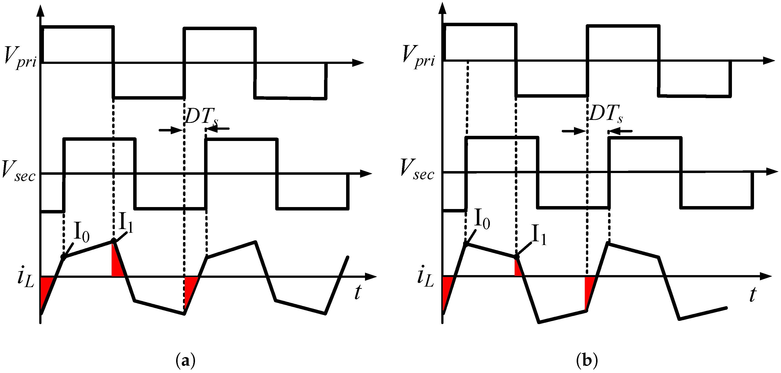
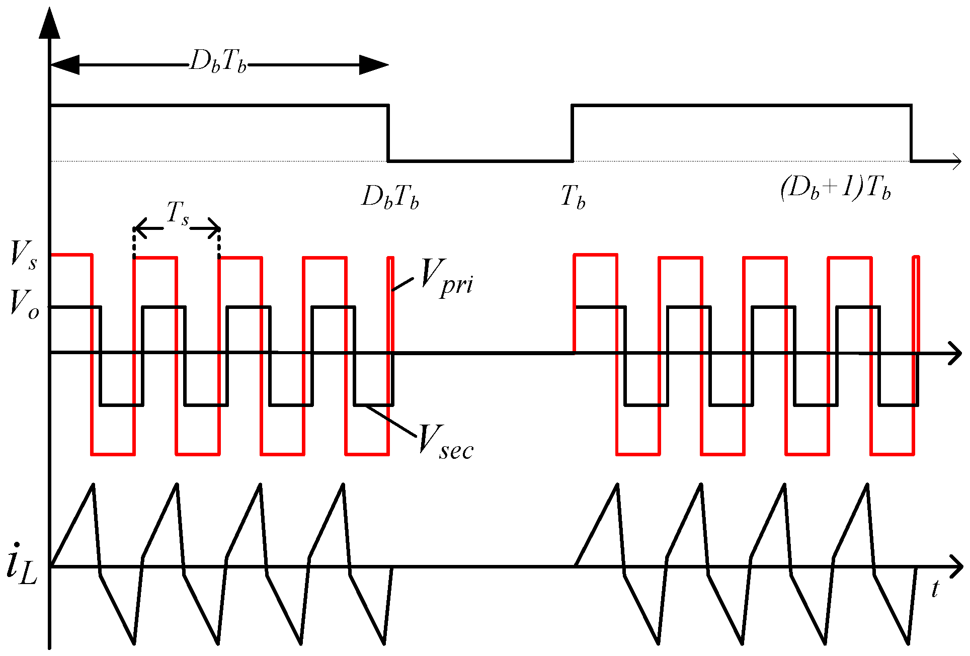
3.1. Burst-Mode Operation
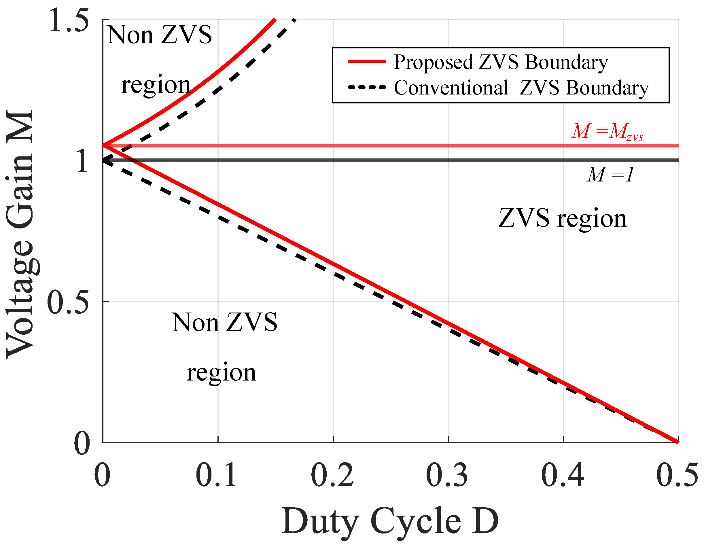
In this burst-mode operation, the PWM signal will be turned on with the burst-mode period T b , and thus, the burst duty D b is used as a control variable for regulating the output voltage V o , as shown in Figure 4. When the burst-mode is applied to the DAB converter, the voltage gain can be expressed as
M b = M D b .
Substituting (2) into (6), the voltage gain is derived as
M b = D ( 1 D ) T s R L 2 L n 2 D b .
It should be noted that the output voltage can be regulated by either the regular duty cycle, D, or the burst-mode duty cycle, D b , as shown in Figure 5.
To minimize the backflow power in the burst-mode, the DAB converter should be operated at the optimally calculated duty cycle D o p . The optimal duty cycle D o p for the minimum backflow power of the DAB converter can be found when the backflow power in (4) is set to zero. As such, the optimal duty cycle D o p can be expressed as
D o p = 1 2 1 M b n V s V o D o p = 1 2 1 1 M b n V s < V o .
While the minimum backflow power in burst-mode is achieved by D o p , the output voltage can be regulated by D b . Substituting D o p into D in (7), the updated voltage gain formula, M b is written as
M b = D o p ( 1 D o p ) T s R L 2 L n 2 D b .
For widely varying output voltage application with maximum and minimum voltages, M m a x and M m i n , the maximum and minimum optimal duty cycles D o p , m i n and D o p , m a x can be calculated; thus, the recommended operation region can be determined as shown in Figure 5.

3.2. ZVS Condition

In the conventional way, ZVS condition in burst-mode can be given by
D o p > 1 2 1 M b D b n V s V o D o p > 1 2 1 D b M b n V s < V o .
Substituting (10) into (9), the ZVS condition is found to be
D b > 2 L n 2 ( 1 2 D o p ) D o p ( 1 D o p ) T s R L n V s V o D b > 2 L n 2 D o p ( 1 2 D o p ) ( 1 D o p ) T s R L n V s < V o .
This means that with the given load condition, the series inductor L can be optimally designed to achieve the ZVS condition. By performing this, minimum backflow and ZVS operation can be achieved simultaneously in the proposed burst-mode.
In the above conventional method, current direction is considered for deriving the ZVS condition. However, the positive or negative direction of the current does not always guarantee soft switching in MOSFETs [30,31]. To further elaborate on the ZVS condition, the energy in the output capacitors of the MOSFETs in the full-bridge should be considered as well [30,31]. As such, the ZVS condition is given by
1 2 L i L 2 ( t ) 2 Q o s s ( V s ) V o
where Q o s s ( V s ) is the total stored charge of the output MOSFET capacitor C o s s at input voltage V s . Substituting (1) into (12), the ZVS condition considering the parasitic capacitance is derived as
D > 1 2 1 M b D b 1 8 Q o s s ( V s ) V o L V s T s n V s V o D > 1 2 1 D b M b 1 8 n Q o s s ( V s ) V o L V o T s n V s < V o .
The further updated optimal duty cycle D o p for ZVS and minimum backflow is given by
D o p = 1 2 1 M b D b 1 8 Q o s s ( V s ) V o L V s T s n V s V o D o p = 1 2 1 D b M b 1 8 n Q o s s ( V s ) V o L V o T s n V s < V o .
The ZVS boundary considering the parasitic capacitances of the MOSFETs is shown as Figure 6. From (14), the adjusted voltage gain for achieving ZVS condition for the entire load condition M z v s can be calculated as
M z v s = 1 8 Q o s s ( V s ) V o L V s T s 1 8 n Q o s s ( V s ) V o L V o T s .
It should be noted that the value of M z v s is not unity as is in the conventional method and is slightly shifted upward.

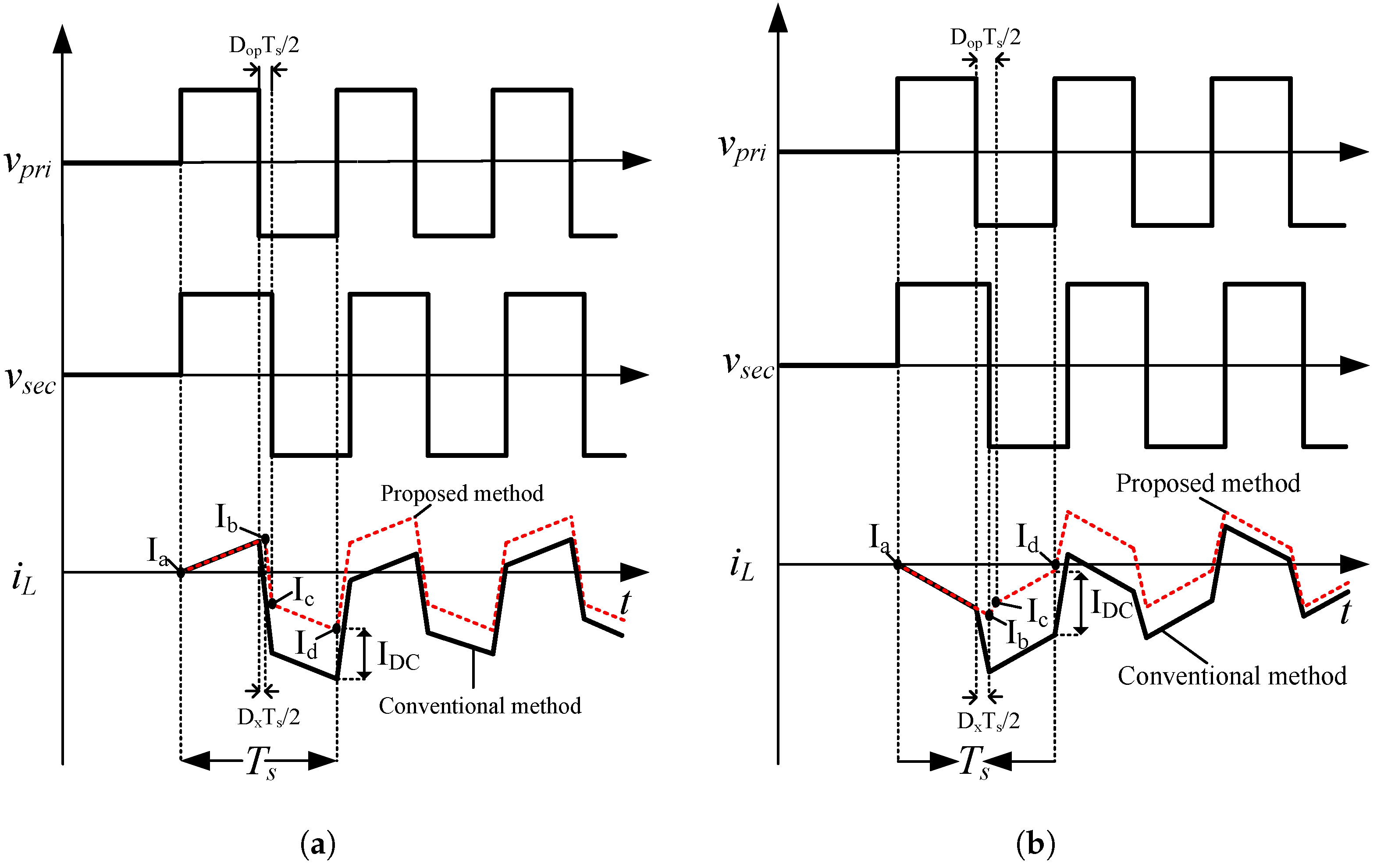
3.3. DC Bias Elimination

In the burst-mode operation, the series inductor current i L jumps from zero to the burst-mode current. In this case, DC bias I D C occurs as shown in Figure 7, which may cause transformer saturation [27,28]. To eliminate the DC bias current, the additional duty cycle D x can be introduced to the optimal regular duty D o p to cancel this effect. The value of D x can be calculated by simple algebraic manipulation.
In the burst-mode operation, the vertex value of the series inductor current i L for both buck and boost mode can be expressed as follows:
I a = 0 I b = I a + n V s V o L 1 + D x T s 2 I c = I b n V s + V o L D o p D x T s 2 I d = I c n V s V o L 1 D o p T s 2 ,
By arranging (16), the DC bias I D C can be expressed as
I D C = D x n V s D o p V o T s L
At steady state, when the DC bias is zero, the value of I d can be expressed as
I d = V s + V o n 2 D o p 1 T s 4 L .
By substituting (18) into (16), the value of D x for zero bias current is given by
D x = 1 4 M ( 2 D o p + 1 ) 1
In order to not disturb the optimal duty operation, the additional duty cycle is applied only for the first pulse of each burst-mode cycle, and its formula is given by
D n = D o p + D x .

4. Design Procedure

Based on to the analysis in Section 3, we developed the design procedure, which is established in this section. Choosing a series inductance L is a critical design step, as it impacts power transfer, efficiency, and control dynamics. The series inductance L should enable efficient power transfer based on the converter’s rated power, input and output voltage levels, and switching frequency. Upon rearranging the power transfer formula in (3), the series inductance L should be satisfied as
L V s V o D ( 1 D ) 2 n f s P o , m a x .
where P o , m a x is the output power at the maximum load condition. In the proposed burst-mode control, the DAB converter achieves the zero-voltage-switching (ZVS) condition and the minimum backflow power at the same time. Therefore, (12) should be satisfied when the series inductor current at optimal duty condition is given by
L 4 Q o s s ( V s ) V o I L , Z V S 2
where I L , Z V S = min ( I o , D o p , I 1 , D o p ) , I 0 , D o p and I 1 , D o p are series inductor currents at optimal duty D o p . With the combined condition of (21) and (22), the series inductor L of the DAB should be within the following specified range:
4 Q o s s ( V s ) V o I L , Z V S 2 L V s V o D ( 1 D ) 2 n f s P o .
Choosing the burst-mode frequency f b in burst-mode control is an important factor which directly affects the efficiency, output ripple, and response time of the power converter, particularly under light-load conditions. A higher f b results in smaller output ripple voltage, but can lead to higher switching losses. Therefore, burst-mode frequency f b should be chosen to balance those factors. In this paper, the burst-mode frequency is chosen as 2.5 kHz.
From the updated voltage gain formula in (9), it can be realized that when the duty cycle D is fixed at the optimal duty cycle D op for the minimum backflow power, the burst duty cycle D b should be used to regulate the output voltage while in the burst-mode, and it is determined by
D b = 2 M b L n 2 D o p ( 1 D o p ) T s R L .
As can be seen from (24), the burst-mode duty cycle D b is a function of the load resistance R L . It is well known that the range of the burst duty cycle is 0 D b 1 . Therefore, the critical load value R c r i t i c a l for the mode switching between the burst-mode and the normal mode of the DAB converter is determined as shown in Figure 8a, and its formula is given by
R c r i t i c a l = 2 M b L n 2 D b D o p ( 1 D o p ) T s .
Notably, the output filter capacitor C o plays a very important role in the burst-mode. Since the power is directly supplied from C o to the load under the burst-mode, the maximum allowable output voltage ripple V o , m a x is directly related to the capacitance value of C o , as shown below:
C o = I o V o , m a x V o f b .
where I o is the output current of the DAB converter. By substituting (26) into (24), the burst duty cycle D b can be rewritten as
D b = 2 M b L n 2 D o p ( 1 D o p ) T s f b C o V o , m a x V o V o .
It should be noted that with a given maximum allowable output voltage ripple V o , m a x , a higher f b would lead to a smaller C o . The burst-mode duty cycle D b versus burst frequency f b can be plotted as shown in Figure 8b; therefore, the burst-mode frequency f b is also determined. The design process of the proposed burst-mode is shown in Figure 9 and detailed as follows:
Step 1:
The initial system parameters such as V s , V o , P o f s , f b , and V o , m a x are given by the system requirement.
Step 2:
The value of inductance L can be calculated by (3).
Step 3:
The voltage gain M b and the optimal duty cycle D op can be calculated by (2) and (14).
Step 4:
The critical load resistance value R c r i t i a l is calculated by (25).
Step 5:
Output capacitor value C o is calculated by (26).
Step 6:
The value of series inductance L should be satisfied by (23). If it is not satisfied, then the design procedure is repeated from Step 3. If the condition is met, the design procedure is finished.

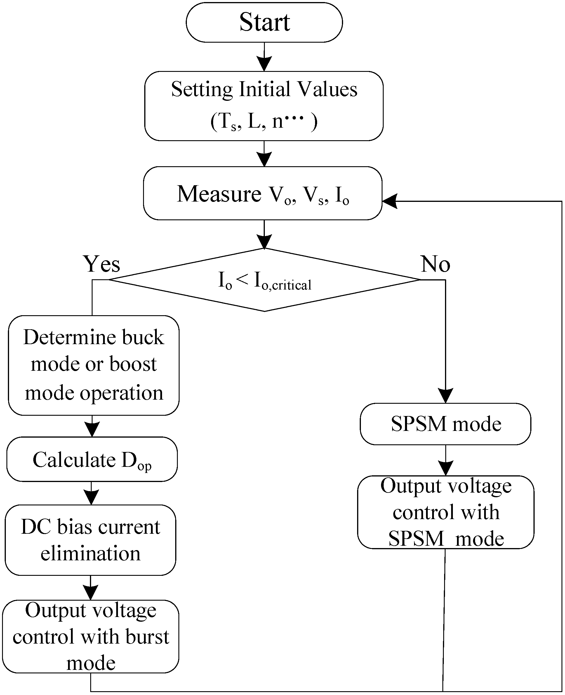
5. Control Mode Switching

The control mode sequence is presented in this section for the dynamic operation of the DAB converter. The critical value of the output current I o , c r i t i c a l can be calculated by the resistance value R c r i t i a l and the output voltage V o , which can be used for the mode change condition. Whenever the measured output current I o is smaller than I o , c r i t i c a l the burst-mode is activated. The proposed burst-mode is, therefore, used as the optimal duty cycle D o p is calculated for minimum backflow power as well as the ZVS condition of the proposed burst-mode. The operation mode of the DAB converter for buck mode or boost mode is determined by comparing the value of n V s with V s . If n V s V o , the buck operation mode is used; otherwise, the boost operation mode is applied. The DC bias current elimination is applied at the first switching period. Moreover, the output voltage V o is regulated by the burst-mode duty cycle D b . If I o becomes larger than I o , c r i t i c a l , the normal SPS mode is activated and the output voltage is regulated by the regulation duty cycle D. The burst-mode period T b can be used as the update period for this sequence. The overall control flowchart of the proposed system is shown in Figure 10.

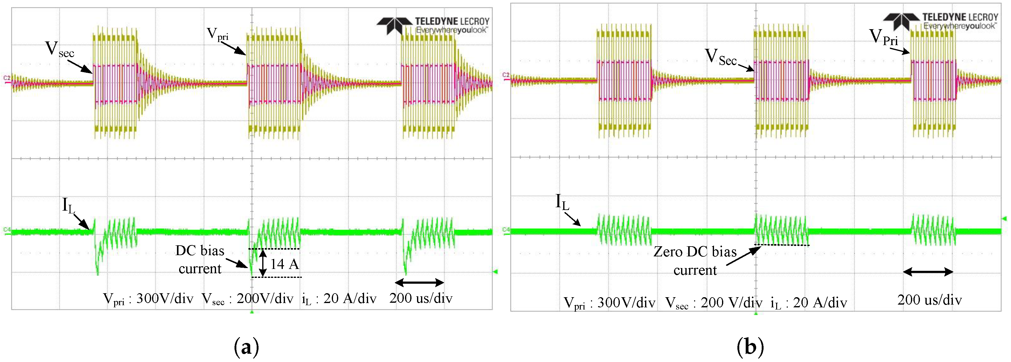
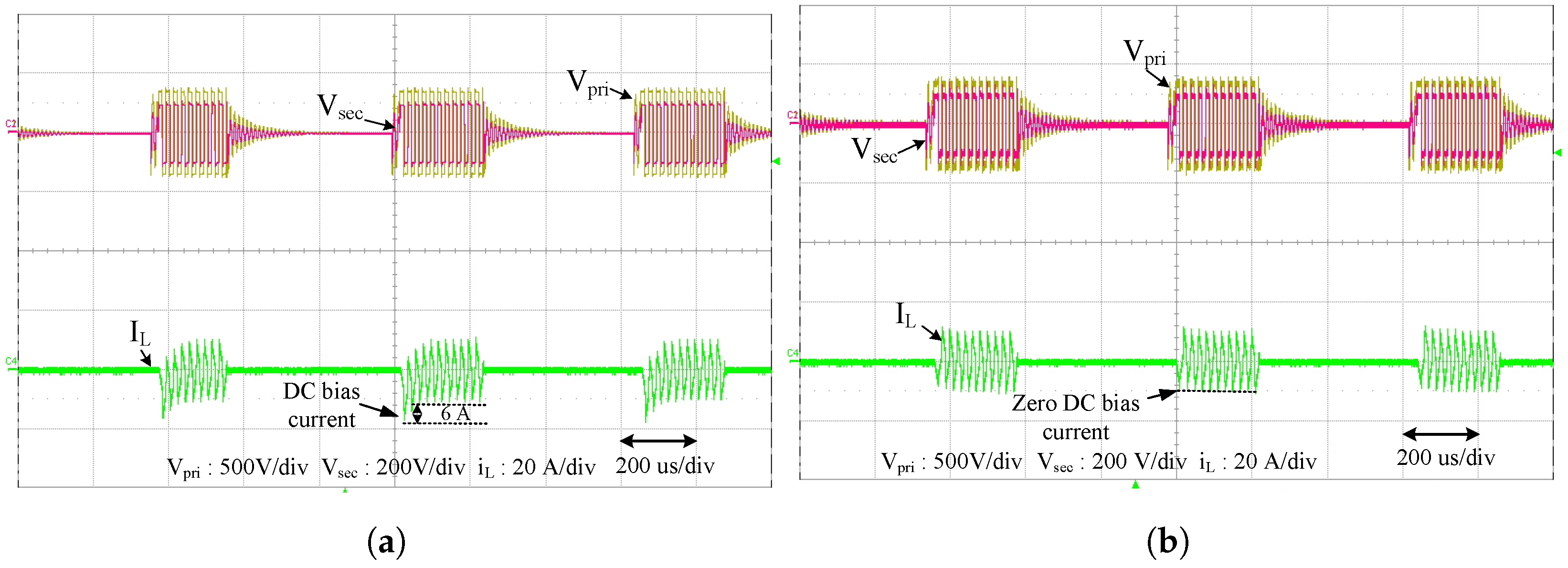
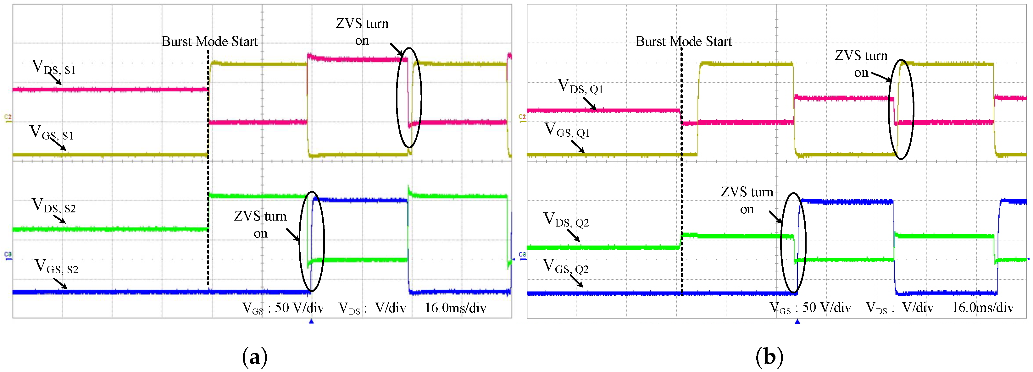
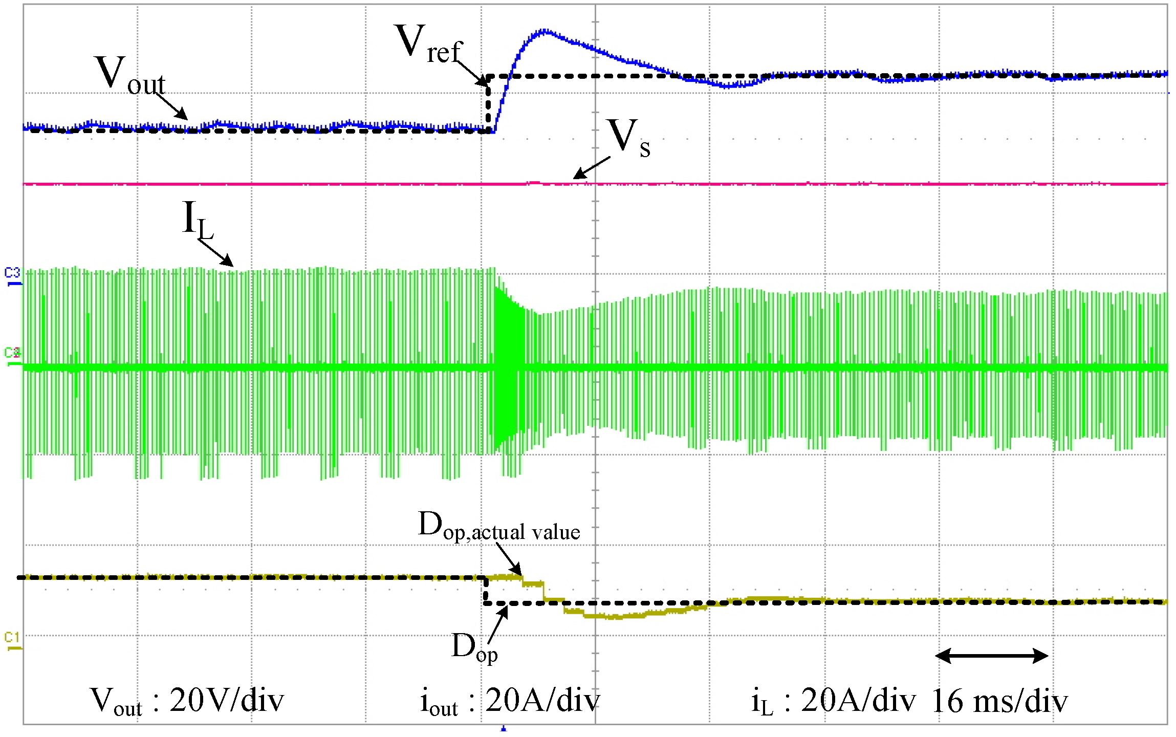
6. Experimental Verification

To verify the proposed control strategy, a 4 kW DAB converter prototype was built as shown in Figure 11. The design procedure in Section 4 is applied to design the system parameters shown in Table 2. The DSP (TMS320F28335 from Texas Instruments, Dallas, TX, USA) is used as the digital controller for algorithm implementation. The MOSFET module (F4-17MR12W1M1H B76 from Infineon, Augsburg, Germany) is used for the main power switches. A power analyzer (Yokogawa Electric, WT1804E, Tokyo, Japan) is used for efficiency measurement. Several experimental tests are conducted to verify the performance of the proposed burst-mode control, which have been performed with a buck-mode configuration.
In case of the conventional burst-mode without DC bias elimination, there are 14 A DC and 6 A DC bias currents for buck and boost modes while starting up the PWM of the burst-mode as shown in Figure 12a and Figure 13a. In the proposed method, after the DC bias current elimination is activated, there is zero bias current as shown in Figure 12b and Figure 13b. Moreover, when SPS modulation is applied, the ZVS condition of switches S 1 and S 2 are similar with switches S 3 and S 4 , and thus, only ZVS of switches S 1 and S 2 are checked. As shown in Figure 14a, ZVS is achieved at the primary side switches. Likewise, ZVS is achieved at the secondary side switches as shown in Figure 14b.
The step change of the output voltage V o is also tested when V r e f steps up from 90 V to 120 V. The output voltage V o can be regulated well with the reference value. Moreover, the optimal duty cycle D o p is changed from 0.275 to 0.2 when the V o is increased from 90 V to 120 V, which matches well with the calculated value in Figure 15.
The load current is increased from 1.5 A to 3 A when the load resistance is changed from 80 Ω to 40 Ω . The undershoot of the output voltage is 4 V, which is 4% of the steady-state output voltage as shown in Figure 16.
The mode switching operation of the proposed control strategy is also tested: burst-mode to normal mode and normal mode to burst-mode. In the case of burst-mode to normal mode, the load resistance is reduced from 80 Ω to 40 Ω when the output current changes from 1.5 A to 3 A. During the mode switching, the output voltage can be regulated with a slight undershoot as shown in Figure 17a. Moreover, in the case of normal mode to burst-mode, when the load resistance is increased from 40 Ω to 80 Ω , the output current changes from 3 A to 1.5 A. During the mode change, the output voltage can be regulated with a slight overshoot as shown in Figure 17b.
The three different voltage gains M = 0.5, 0.9, and 1.3 are tested to verify the effectiveness of the proposed burst-mode control method over the conventional method. In the proposed burst-mode control, the duty cycle D is equal to the optimal duty cycle D o p which is equal to 0.256, 0.06, and 0.116 while M = 0.5, 0.9, and 1.3, respectively. However, the duty cycle D is fixed for all voltage gain conditions in conventional burst-mode control, which is 0.17 and 0.34. Due to the ZVS operation and minimum backflow power, the efficiency of the proposed method is always higher than conventional burst-mode control as shown in Figure 18. The efficiency improvement of the proposed burst-mode control can be more significant, in case higher-frequency operations are used due to the whole-load range ZVS feature.

7. Conclusions

In order to achieve ZVS for the whole operation range and improve efficiency of light-load conditions, the burst-mode for the SPS modulation of the DAB converter is proposed in this paper. With the proposed burst-mode, the DAB converter is operated with minimum backflow power as well as achieving ZVS under light-load conditions. Therefore, the system efficiency is significantly improved. The DC bias current issue of the conventional burst-mode is also mitigated in the proposed method. The detailed analysis of proposed burst-mode operation of the DAB converter is derived for both buck and boost operation modes. The detailed design procedure of the DAB converter for the burst-mode control is also presented. Moreover, the proposed burst-mode control flowchart is also presented for achieving ZVS in all load conditions. Therefore, the efficiency of the whole load range condition is also improved. The effectiveness of the proposed burst-mode is verified by experiment. The system efficiency can be improved by 2% compared with the conventional burst-mode method.

Author Contributions

S.-J.C. proposed the basic concept of this paper, C.-T.T. contributed to the mathematical formulation and wrote the original manuscript, B.-R.N. contributed to the investigation and simulation, and J.-S.P. contributed to hardware implementation. All authors have read and agreed to the published version of the manuscript.

Funding

This work was supported by the Regional Innovation Strategy (RIS) through the National Research Foundation of Korea (NRF), funded by the Ministry of Education (MOE) (2021RIS-003), and in part by National Research Foundation of Korea (NRF) grant, funded by the Korea government (MSIT) (RS-2023-00240194).

Data Availability Statement

The original contributions presented in the study are included in the article, further inquiries can be directed to the corresponding author.

Conflicts of Interest

The authors declare no conflicts of interest.

References

  1. Kheraluwala, M.; Gascoigne, R.; Divan, D.; Baumann, E. Performance characterization of a high-power dual active bridge DC-to-DC converter. IEEE Trans. Ind. Appl. 1992, 28, 1294–1301. [Google Scholar] [CrossRef]
  2. Zhao, B.; Song, Q.; Liu, W.; Sun, Y. Overview of Dual-Active-Bridge Isolated Bidirectional DC–DC Converter for High-Frequency-Link Power-Conversion System. IEEE Trans. Power Electron. 2014, 29, 4091–4106. [Google Scholar] [CrossRef]
  3. De Doncker, R.; Divan, D.; Kheraluwala, M. A three-phase soft-switched high-power-density DC/DC converter for high-power applications. IEEE Trans. Ind. Appl. 1991, 27, 63–73. [Google Scholar] [CrossRef]
  4. Chen, X.; Xu, G.; Han, H.; Liu, D.; Sun, Y.; Su, M. Light-Load Efficiency Enhancement of High-Frequency Dual-Active-Bridge Converter Under SPS Control. IEEE Trans. Ind. Electron. 2021, 68, 12941–12946. [Google Scholar] [CrossRef]
  5. Bai, H.; Mi, C. Eliminate Reactive Power and Increase System Efficiency of Isolated Bidirectional Dual-Active-Bridge DC–DC Converters Using Novel Dual-Phase-Shift Control. IEEE Trans. Power Electron. 2008, 23, 2905–2914. [Google Scholar] [CrossRef]
  6. Shi, H.; Wen, H.; Chen, J.; Hu, Y.; Jiang, L.; Chen, G.; Ma, J. Minimum-Backflow-Power Scheme of DAB-Based Solid-State Transformer With Extended-Phase-Shift Control. IEEE Trans. Ind. Appl. 2018, 54, 3483–3496. [Google Scholar] [CrossRef]
  7. Lee, S.H.; Kim, B.K.; Kim, S. Single pulse width modulation for dual-active-bridge converters considering parasitic capacitance of MOSFETs. J. Power Electron. 2023, 23, 68–78. [Google Scholar] [CrossRef]
  8. Heo, K.W.; Yun, C.W.; Jung, G.G.; Lee, J.S.; Kim, H.S.; Jung, J.H. Enhanced four-port dual-active-bridge converter employing power decoupling capability for DC microgrid islanding mode operation. J. Power Electron. 2024, 24, 171–180. [Google Scholar] [CrossRef]
  9. Zhao, B.; Yu, Q.; Sun, W. Extended-Phase-Shift Control of Isolated Bidirectional DC–DC Converter for Power Distribution in Microgrid. IEEE Trans. Power Electron. 2012, 27, 4667–4680. [Google Scholar] [CrossRef]
  10. Bai, H.; Nie, Z.; Mi, C.C. Experimental Comparison of Traditional Phase-Shift, Dual-Phase-Shift, and Model-Based Control of Isolated Bidirectional DC–DC Converters. IEEE Trans. Power Electron. 2010, 25, 1444–1449. [Google Scholar] [CrossRef]
  11. Huang, J.; Wang, Y.; Li, Z.; Lei, W. Unified Triple-Phase-Shift Control to Minimize Current Stress and Achieve Full Soft-Switching of Isolated Bidirectional DC–DC Converter. IEEE Trans. Ind. Electron. 2016, 63, 4169–4179. [Google Scholar] [CrossRef]
  12. Zhang, C.; Zhou, Y.; Yu, D. Self-Adapting Voltage Balancing Method for IPOS DAB Converter with TPS Control. IEEE Trans. Appl. Supercond. 2024, 34, 5702706. [Google Scholar] [CrossRef]
  13. Li, H.; Song, C.; Zhao, X.; Zhang, H.; Wang, M.; Li, G.; Guo, H.; Hou, N. Direct Phase-Shift-Angle Optimization Strategy for DAB Converters’ Efficiency Enhancement Based on Fundamental Extended Phase-Shift Modulation. IEEE J. Emerg. Sel. Top. Power Electron. 2024, 12, 4678–4690. [Google Scholar] [CrossRef]
  14. Shao, S.; Chen, L.; Shan, Z.; Gao, F.; Chen, H.; Sha, D.; Dragičević, T. Modeling and Advanced Control of Dual-Active-Bridge DC–DC Converters: A Review. IEEE Trans. Power Electron. 2022, 37, 1524–1547. [Google Scholar] [CrossRef]
  15. Rodríguez Alonso, A.R.; Sebastian, J.; Lamar, D.G.; Hernando, M.M.; Vazquez, A. An overall study of a Dual Active Bridge for bidirectional DC/DC conversion. In Proceedings of the 2010 IEEE Energy Conversion Congress and Exposition, Atlanta, GA, USA, 12–16 September 2010; pp. 1129–1135. [Google Scholar] [CrossRef]
  16. Wang, F.; Cui, X.; Zhuo, F.; Tian, J.; Zheng, Z.; Xu, R. Novel asymmetric duty modulation for DAB converters to improve light load efficiency. J. Power Electron. 2023, 23, 592–606. [Google Scholar] [CrossRef]
  17. Chan, Y.P.; Loo, K.H.; Yaqoob, M.; Lai, Y.M. A Structurally Reconfigurable Resonant Dual-Active-Bridge Converter and Modulation Method to Achieve Full-Range Soft-Switching and Enhanced Light-Load Efficiency. IEEE Trans. Power Electron. 2019, 34, 4195–4207. [Google Scholar] [CrossRef]
  18. Li, L.; Xu, G.; Sha, D.; Liu, Y.; Sun, Y.; Su, M. Review of Dual-Active-Bridge Converters with Topological Modifications. IEEE Trans. Power Electron. 2023, 38, 9046–9076. [Google Scholar] [CrossRef]
  19. Truong, C.T.; Choi, S.J. Analysis of Capacitor Parasitic Effects on Output Voltage Ripple and Load Transient of DAB Converters. In Proceedings of the 2023 11th International Conference on Power Electronics and ECCE Asia (ICPE 2023—ECCE Asia), Jeju, Republic of Korea, 22–25 May 2023; pp. 2885–2891. [Google Scholar] [CrossRef]
  20. Feng, W.; Lee, F.C.; Mattavelli, P. Optimal Trajectory Control of Burst Mode for LLC Resonant Converter. IEEE Trans. Power Electron. 2013, 28, 457–466. [Google Scholar] [CrossRef]
  21. Cortes, D.; Hernandez-Gonzalez, L.; Ramirez-Hernandez, J.; Vargas, M. Modeling and Control of an Inductive Power Transmitter Based on Buck–Half Bridge–Resonant Tank. Electronics 2024, 13, 1593. [Google Scholar] [CrossRef]
  22. Carbajal-Retana, M.; Hernandez-Gonzalez, L.; Ramirez-Hernandez, J.; Avalos-Ochoa, J.G.; Guevara-Lopez, P.; Loboda, I.; Sotres-Jara, L.A. Interleaved buck converter for inductive wireless power transfer in DC–DC converters. Electronics 2020, 9, 949. [Google Scholar] [CrossRef]
  23. Shi, L.; Liu, B.; Duan, S. Burst-mode and phase-shift hybrid control method of LLC converters for wide output range applications. IEEE Trans. Ind. Electron. 2019, 67, 1013–1023. [Google Scholar] [CrossRef]
  24. Huang, C.; Mannen, T.; Isobe, T. Improved Burst Mode Operation for DAB Converters to Achieve ZVS in Full-Load-Range by Considering Device Voltage Oscillation. In Proceedings of the 2023 IEEE 24th Workshop on Control and Modeling for Power Electronics (COMPEL), Ann Arbor, MI, USA, 25–28 June 2023; pp. 1–7. [Google Scholar] [CrossRef]
  25. Yao, Y.; Kulothungan, G.S.; Krishnamoorthy, H.S. Improved Circuit Design and Adaptive Burst Mode Control in PSFB Converters for Higher Efficiency Over a Wide Power Range. IEEE Access 2022, 10, 9152–9163. [Google Scholar] [CrossRef]
  26. Iyer, V.M.; Gulur, S.; Bhattacharya, S. Hybrid control strategy to extend the ZVS range of a dual active bridge converter. In Proceedings of the 2017 IEEE Applied Power Electronics Conference and Exposition (APEC), Tampa, FL, USA, 26–30 March 2017; pp. 2035–2042. [Google Scholar] [CrossRef]
  27. Bu, Q.; Wen, H.; Shi, H.; Zhu, Y. A Comparative Review of High-Frequency Transient DC Bias Current Mitigation Strategies in Dual-Active-Bridge DC–DC Converters Under Phase-Shift Modulations. IEEE Trans. Ind. Appl. 2022, 58, 2166–2182. [Google Scholar] [CrossRef]
  28. Zhao, B.; Song, Q.; Liu, W.; Zhao, Y. Transient DC Bias and Current Impact Effects of High-Frequency-Isolated Bidirectional DC–DC Converter in Practice. IEEE Trans. Power Electron. 2016, 31, 3203–3216. [Google Scholar] [CrossRef]
  29. Li, X.; Li, Y.F. An Optimized Phase-Shift Modulation For Fast Transient Response in a Dual-Active-Bridge Converter. IEEE Trans. Power Electron. 2014, 29, 2661–2665. [Google Scholar] [CrossRef]
  30. Yan, Y.; Gui, H.; Bai, H. Complete ZVS Analysis in Dual Active Bridge. IEEE Trans. Power Electron. 2021, 36, 1247–1252. [Google Scholar] [CrossRef]
  31. Truong, C.T.; Choi, S.J. Improved ZVS Criterion for Series Resonant Converters. IEEE Access 2024, 12, 5333–5344. [Google Scholar] [CrossRef]
  32. Na, B.R.; Park, J.S.; Truong, C.T.; Choi, S.J. Novel Burst-mode Control Strategy for Enhanced Light-load Efficiency of DAB Converters. In Proceedings of the 2024 IEEE Energy Conversion Congress and Exposition (ECCE), Phoenix, AZ, USA, 20–24 October 2024; pp. 2691–2697. [Google Scholar]
  33. Oggier, G.G.; Ordonez, M. High-Efficiency DAB Converter Using Switching Sequences and Burst Mode. IEEE Trans. Power Electron. 2016, 31, 2069–2082. [Google Scholar] [CrossRef]
Figure 1. Isolated DAB converter.
Energies 17 05748 g001
Figure 2. Key operation waveforms of the DAB converter with SPS modulation control: (a) buck operation mode and (b) boost operation mode.
Energies 17 05748 g002
Figure 3. ZVS condition and backflow power for different voltage gains and load conditions.
Energies 17 05748 g003
Figure 4. Burst-mode operation waveform.
Energies 17 05748 g004
Figure 5. Determination of the operation region for proposed burst-mode control.
Energies 17 05748 g005
Figure 6. ZVS condition boundary with the new ZVS condition.
Energies 17 05748 g006
Figure 7. DC bias elimination key waveforms of the proposed burst-mode control in (a) buck operation mode and (b) boost operation mode.
Energies 17 05748 g007
Figure 8. (a) Critical load value R c r i t i c a l for mode change condition; (b) the burst-mode duty cycle D b versus burst frequency f b .
Energies 17 05748 g008
Figure 9. Design procedure of the proposed burst-mode method.
Energies 17 05748 g009
Figure 10. Proposed burst-mode control flowchart.
Energies 17 05748 g010
Figure 11. Experimental setup: (a) prototype DAB converter; (b) DC power supply, electronic load, and measurement equipment.
Energies 17 05748 g011
Figure 12. Experimental waveforms of DC bias elimination for buck operation mode: (a) conventional burst-mode and (b) proposed burst-mode.
Energies 17 05748 g012
Figure 13. Experimental waveforms of DC bias current elimination for boost operation mode: (a) conventional burst-mode and (b) proposed burst-mode.
Energies 17 05748 g013
Figure 14. Experimental waveforms for ZVS of (a) primary side and (b) secondary side.
Energies 17 05748 g014
Figure 15. Experimental waveforms of the proposed burst-mode control when V ref changes from 90 V to 120 V.
Energies 17 05748 g015
Figure 16. Experimental waveforms of DAB converter of the proposed burst-mode control when load changes from 80 Ω to 40 Ω .
Energies 17 05748 g016
Figure 17. Experimental waveforms of the mode switching (a) from burst-mode to normal mode and (b) from the normal mode to burst-mode.
Energies 17 05748 g017
Figure 18. Efficiency measurement comparison for (a) M = 0.5 (b) M = 0.9 (c) M = 1.3 .
Energies 17 05748 g018
Table 1. Comparisons with previous control methods.
Ref.Type of ControlSoft-Switching RangeMinimum Backflow PowerImplementation ComplexityDC Bias Elimination
[4]SPSPartialNoLowNo
[9]EPSPartialYesMediumNo
[10]DPSPartialYesMediumNo
[11]TPSFullYesHighNo
[33]SPS + burst-modePartialNoLowNo
This paperSPS + burst-modeFullYesLowYes
Table 2. System parameters.
SymbolParametersValuesCalculatedUnit
V s DC input voltage400 V
V o DC output voltage100–180 V
f s Switching frequency50 kHz
P o Output power0–4 kW
n Transformer turn ratio2:1
C o Output filter capacitance500450 μ F
L Series inductance5044 μ H
f b Burst frequency2.5 kHz
R critical Critical value of load resistance5050.16 Ω
Disclaimer/Publisher’s Note: The statements, opinions and data contained in all publications are solely those of the individual author(s) and contributor(s) and not of MDPI and/or the editor(s). MDPI and/or the editor(s) disclaim responsibility for any injury to people or property resulting from any ideas, methods, instructions or products referred to in the content.

