
Optimizing the Band Alignment of the MZO/CdSeTe/CdTe Solar Cell by Varying the Substrate Temperature of MZO Film

 ,
,
Abstract
:
1. Introduction
2. Materials and Methods
2.1. Preparation and Characterization of MZO Film
2.2. Device Fabrication and Characterization
3. Results
3.1. Substrate Temperature Effect on Optical Property, Composition, Crystal Structure, and Chemical State of MZO Film
3.2. I-V Test Result of MZO Films Applied in CdSeTe/CdTe Solar Cells
4. Discussion
5. Conclusions
Author Contributions
Funding
Data Availability Statement
Conflicts of Interest
References
- Scarpulla, M.A.; McCandless, B.; Phillips, A.B.; Yan, Y.; Heben, M.J.; Wolden, C.; Xiong, G.; Metzger, W.K.; Mao, D.; Krasikov, D.; et al. CdTe-based thin film photovoltaics: Recent advances, current challenges and future prospects. Sol. Energy Mater. Sol. Cells 2023, 255, 112289. [Google Scholar] [CrossRef]
- Ohyama, H.; Aramoto, T.; Kumazawa, S.; Higuchi, H.; Arita, T.; Shibutani, S.; Nishio, T.; Nakajima, J.; Tsuji, M.; Hanafusa, A.; et al. 16.0% efficient thin-film CdS/CdTe solar cells. In Proceedings of the Conference Record of the Twenty Sixth IEEE Photovoltaic Specialists Conference, Anaheim, CA, USA, 29 September–3 October 1997; pp. 343–346. [Google Scholar] [CrossRef]
- Romeo, A.; Artegiani, E. CdTe-Based Thin Film Solar Cells: Past, Present and Future. Energies 2021, 14, 1684. [Google Scholar] [CrossRef]
- Meysing, D.M.; Wolden, C.A.; Griffith, M.M.; Mahabaduge, H.; Pankow, J.; Reese, M.O.; Burst, J.M.; Rance, W.L.; Barnes, T.M. Properties of reactively sputtered oxygenated cadmium sulfide (CdS:O) and their impact on CdTe solar cell performance. J. Vac. Sci. Technol. A 2014, 33, 021203. [Google Scholar] [CrossRef]
- Kephart, J.; McCamy, J.; Ma, Z.; Ganjoo, A.; Alamgir, F.; Sampath, W. Band alignment of front contact layers for high-efficiency CdTe solar cells. Sol. Energy Mater. Sol. Cells 2016, 157, 266–275. [Google Scholar] [CrossRef]
- Kephart, J.M.; Kindvall, A.; Williams, D.; Kuciauskas, D.; Dippo, P.; Munshi, A.; Sampath, W.S. Sputter-Deposited Oxides for Interface Passivation of CdTe Photovoltaics. IEEE J. Photovoltaics 2018, 8, 587–593. [Google Scholar] [CrossRef]
- Munshi, A.H.; Kephart, J.; Abbas, A.; Raguse, J.; Beaudry, J.-N.; Barth, K.; Sites, J.; Walls, J.; Sampath, W. Polycrystalline CdSeTe/CdTe Absorber Cells With 28 mA/cm2 Short-Circuit Current. IEEE J. Photovoltaics 2017, 8, 310–314. [Google Scholar] [CrossRef]
- Pandey, R.; Munshi, A.; Shimpi, T.; Shah, A.; Bothwell, A.; Kuciauskas, D.; Sites, J.R. CdTe-Based Solar Cells with Variations in Mg Concentration in the MgZnO Emitter. Sol. RRL 2021, 5, 2100126. [Google Scholar] [CrossRef]
- Wang, T.; Ren, S.; Li, C.; Li, W.; Liu, C.; Zhang, J.; Wu, L.; Li, B.; Zeng, G. Exploring window buffer layer technology to enhance CdTe solar cell performance. Sol. Energy 2018, 164, 180–186. [Google Scholar] [CrossRef]
- Menossi, D.; Artegiani, E.; Bittau, F.; Barbato, M.; Meneghini, M.; Meneghesso, G.; Bowers, J.; Walls, M.; Piccinelli, F.; Romeo, A. High Efficiency CdTe Solar Cells by Low Temperature Deposition with MgZnO HRT Layer. In Proceedings of the 33rd European Photovoltaic Solar Energy Conference and Exhibition, Amsterdam, The Netherlands, 25–29 September 2017; pp. 1027–1030. [Google Scholar] [CrossRef]
- Ablekim, T.; Perkins, C.; Zheng, X.; Reich, C.; Swanson, D.; Colegrove, E.; Duenow, J.N.; Albin, D.; Nanayakkara, S.; Reese, M.O.; et al. Tailoring MgZnO/CdSeTe Interfaces for Photovoltaics. IEEE J. Photovoltaics 2019, 9, 888–892. [Google Scholar] [CrossRef]
- Song, T.; Kanevce, A.; Sites, J.R. Emitter/absorber interface of CdTe solar cells. J. Appl. Phys. 2016, 119, 233104. [Google Scholar] [CrossRef]
- Kanevce, A.; Reese, M.O.; Barnes, T.M.; Jensen, S.A.; Metzger, W.K. The roles of carrier concentration and interface, bulk, and grain-boundary recombination for 25% efficient CdTe solar cells. J. Appl. Phys. 2017, 121, 214506. [Google Scholar] [CrossRef]
- Ablekim, T.; Colegrove, E.; Metzger, W.K. Interface Engineering for 25% CdTe Solar Cells. ACS Appl. Energy Mater. 2018, 1, 5135–5139. [Google Scholar] [CrossRef]
- Wu, Q.; Zhang, Y.; Li, R.; Huang, K.; Zhao, W.; Liu, X. Effect of direct current bias on MZO window layer in CdTe solar cells. J. Phys. D Appl. Phys. 2023, 56, 41LT01. [Google Scholar] [CrossRef]
- Onno, A.; Reich, C.; Li, S.; Danielson, A.; Weigand, W.; Bothwell, A.; Grover, S.; Bailey, J.; Xiong, G.; Kuciauskas, D.; et al. Understanding what limits the voltage of polycrystalline CdSeTe solar cells. Nat. Energy 2022, 7, 400–408. [Google Scholar] [CrossRef]
- Briggs, D.; Seah, M.P. (Eds.) Surface Analysis; John Wiley & Sons, Inc.: Hoboken, NJ, USA, 2004. [Google Scholar]
- Hwang, D.-K.; Jeong, M.-C.; Myoung, J.-M. Effects of deposition temperature on the properties of Zn1−xMgxO thin films. Appl. Surf. Sci. 2004, 225, 217–222. [Google Scholar] [CrossRef]
- Bittau, F.; Potamialis, C.; Togay, M.; Abbas, A.; Isherwood, P.J.; Bowers, J.W.; Walls, J.M. Analysis and optimisation of the glass/TCO/MZO stack for thin film CdTe solar cells. Sol. Energy Mater. Sol. Cells 2018, 187, 15–22. [Google Scholar] [CrossRef]
- Liu, C.Y.; Xu, H.Y.; Wang, L.; Li, X.H.; Liu, Y.C. Pulsed laser deposition of high Mg-content MgZnO films: Effects of substrate temperature and oxygen pressure. J. Appl. Phys. 2009, 106, 073518. [Google Scholar] [CrossRef]
- Periodic Table of Elements [DB]. Available online: https://www.periodic-table.org/ (accessed on 2 December 2023).
- Gu, K.; Zhou, X.; Zhang, Z.; Tang, K.; Huang, J.; Wang, L. Tailoring microstructure and optical properties of MgZnO film on glass by substrate temperature. Mater. Lett. 2020, 278, 128416. [Google Scholar] [CrossRef]
- Zhao, L.; Shao, G.; Song, S.; Qin, X.; Han, S. Development on transparent conductive ZnO thin films doped with various impurity elements. Rare Met. 2011, 30, 175–182. [Google Scholar] [CrossRef]
- Tu, Y.; Chen, S.; Li, X.; Gorbaciova, J.; Gillin, W.P.; Krause, S.; Briscoe, J. Control of oxygen vacancies in ZnO nanorods by annealing and their influence on ZnO/PEDOT:PSS diode behaviour. J. Mater. Chem. C 2018, 6, 1815–1821. [Google Scholar] [CrossRef]
- Park, S.Y.; Kim, S.; Yoo, J.; Lim, K.-H.; Lee, E.; Kim, K.; Kim, J.; Kim, Y.S. Aqueous zinc ammine complex for solution-processed ZnO semiconductors in thin film transistors. RSC Adv. 2014, 4, 11295–11299. [Google Scholar] [CrossRef]
- Fuchs, A.; Schimper, H.-J.; Klein, A.; Jaegermann, W. Photoemission studies on undoped SnO2 buffer layers for CdTe thin film solar cells. Energy Procedia 2011, 10, 149–154. [Google Scholar] [CrossRef]
- Liu, L.; Mei, Z.; Tang, A.; Azarov, A.; Kuznetsov, A.; Xue, Q.-K.; Du, X. Oxygen vacancies: The origin ofn-type conductivity in ZnO. Phys. Rev. B 2016, 93, 235305. [Google Scholar] [CrossRef]
- Hegedus, S.S.; Shafarman, W.N. Thin-Film Solar Cells: Device Measurements and Analysis. Prog. Photovolt. Res. 2004, 12, 155–176. [Google Scholar] [CrossRef]


| Substrate Temperature (°C) | hkl | 2θ (°) | FWHM (°) |
|---|---|---|---|
| 22 | (0 0 2) | 34.27 | 0.53 |
| 55 | (0 0 2) | 34.44 | 0.52 |
| 103 | (0 0 2) | 34.45 | 0.50 |
| 145 | (0 0 2) | 34.56 | 0.49 |
| 178 | (0 0 2) | 34.44 | 0.51 |
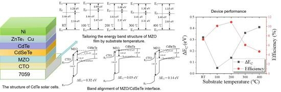
| Substrate Temperature (°C) | Eg MZO (eV) | Eg CdSeTe (eV) | (EF−EV) MZO (eV) | (EF−EV) CdSeTe (eV) | ΔEV (eV) | ΔEC (eV) |
|---|---|---|---|---|---|---|
| RT | 3.44 | 1.44 | 2.18 | 0.50 | −1.63 | 0.32 |
| 100 | 3.44 | 1.44 | 2.45 | 0.50 | −1.95 | 0.05 |
| 200 | 3.43 | 1.44 | 2.35 | 0.50 | −1.85 | 0.14 |
| 300 | 3.41 | 1.44 | 2.11 | 0.50 | −1.61 | 0.36 |
| 400 | 3.40 | 1.44 | 2.05 | 0.50 | −1.55 | 0.41 |
Disclaimer/Publisher’s Note: The statements, opinions and data contained in all publications are solely those of the individual author(s) and contributor(s) and not of MDPI and/or the editor(s). MDPI and/or the editor(s) disclaim responsibility for any injury to people or property resulting from any ideas, methods, instructions or products referred to in the content. |
© 2024 by the authors. Licensee MDPI, Basel, Switzerland. This article is an open access article distributed under the terms and conditions of the Creative Commons Attribution (CC BY) license (https://creativecommons.org/licenses/by/4.0/).
Share and Cite
Wu, Q.; Li, R.; Zhang, Y.; Huang, K.; Li, H.; Liu, X. Optimizing the Band Alignment of the MZO/CdSeTe/CdTe Solar Cell by Varying the Substrate Temperature of MZO Film. Energies 2024, 17, 592. https://doi.org/10.3390/en17030592
Wu Q, Li R, Zhang Y, Huang K, Li H, Liu X. Optimizing the Band Alignment of the MZO/CdSeTe/CdTe Solar Cell by Varying the Substrate Temperature of MZO Film. Energies. 2024; 17(3):592. https://doi.org/10.3390/en17030592
Chicago/Turabian StyleWu, Qiuchen, Ruchun Li, Yufeng Zhang, Kai Huang, Heran Li, and Xiangxin Liu. 2024. "Optimizing the Band Alignment of the MZO/CdSeTe/CdTe Solar Cell by Varying the Substrate Temperature of MZO Film" Energies 17, no. 3: 592. https://doi.org/10.3390/en17030592