Article

Power Loss Modelling and Performance Comparison of Three-Level GaN-Based Inverters Used for Electric Traction

1
STMicroelectronics, Stradale Primo Sole 50, 95121 Catania, Italy
2
Department of Electrical Electronic and Computer Engineering, University of Catania, Via Santa Sofia 64, 95123 Catania, Italy
*
Authors to whom correspondence should be addressed.
Energies 2024, 17(3), 595; https://doi.org/10.3390/en17030595
Submission received: 18 December 2023 / Revised: 11 January 2024 / Accepted: 19 January 2024 / Published: 26 January 2024

Abstract

:
The main aim of this work is to present a step-by-step procedure to model and analyze the power loss distribution of three-level Gallium Nitride (GaN) inverters. It has been applied to three distinct three-phase three-level voltage source inverters utilized in electric traction drives: Active Neutral Point Clamped, Neutral Point Clamped and T-Type Neutral Point Clamped. The proposed analytical power loss modelling, combined with an equivalent representation of the electrical machine proved to be a viable solution to achieve a time-saving and low computational burden simulation platform, leading to satisfying accurate results. This has been confirmed by comparing the results carried out from the simulations of a 110 kW permanent magnet synchronous motor drive and those determined by considering a simplified circuital representation based on the proposed analytical power loss modelling.

1. Introduction

Nowadays, the significance of electric traction is widely acknowledged as fundamental for the advancement of society. Projections indicate substantial growth in the global electric vehicle (EV) market in the upcoming years, largely due to policy objectives aimed at reducing greenhouse gas emissions in transportation across numerous countries worldwide [1,2,3].
Currently, light-duty electric vehicles typically feature powertrains with rated power varying between 60 kW and 200 kW. These powertrains are mostly powered by lithium-ion battery packs with capacities ranging from 30 kWh to 110 kWh, resulting in estimated ranges mostly below 400 km. This limited range stands as a significant barrier hindering the widespread adoption of EVs. Another substantial limitation is the lengthy recharging duration compared to equivalent internal combustion vehicles. Despite significant developments in recharging infrastructure, most charging points still operate at a peak power of 100 kW [4]. Consequently, charging times for reaching 80% battery capacity using 100 kW–480 V DC fast charging typically range from 30 min to 1 h. Reducing charging times would alleviate the inconvenience posed by a limited driving range. Therefore, higher charging power can considerably diminish battery-refueling duration. For instance, increasing fast-charging power levels from 100 kW to 350 kW results in a significant reduction in charging time. However, maintaining the charging voltage at the typical value of 400 V would necessitate increased current ratings for charging cables, leading to amplified system power losses. Some automotive manufacturers are exploring solutions involving an 800 V DC bus to achieve faster battery-charging times [5,6,7,8,9]. However, this approach presents technical challenges related to current electric powertrain technologies, especially semiconductor technologies utilized in electric traction inverters.
Additionally, considering alternative power-converter topologies could potentially enhance efficiency, reliability, and power density, while simultaneously reducing the cost and weight of power-conversion processes.
Because of their notable efficiency and cost-effectiveness, the prevailing choice for most production EVs involves the utilization of two-level (2L) three-phase voltage source inverters (VSIs). These inverters typically rely on insulated gate bipolar transistors (IGBTs), with only a few cases incorporating silicon-carbide-based (SiC) power modules. IGBTs power devices still remain the primary choice for realizing common traction inverters over other available power device technologies. This preference stems from the technology’s maturity, widespread availability, cost-effectiveness, and sufficient power-handling capabilities. IGBTs with blocking voltages ranging from 650 V to 1200 V are well-suited to manage the variable DC-link voltages of today’s battery packs, which typically range from 300 V to 450 V. The VSI topology can be realized using compact power modules, each comprising multiple dies arranged in parallel to evenly distribute the high current load across the switches to reach the appropriate power level. In commercial-vehicle applications, most IGBT-based traction inverters demonstrate efficiencies below 94%. These systems operate at switching frequencies intentionally kept below 30 kHz to limit power losses. Additionally, due to technological limitations inherent in power switches, the dead time between complementary switches is generally set to at least 1 μs. This practice is adopted to mitigate output-current distortion and voltage error, which become more pronounced at higher rotational speeds, consequently impacting on the control performance [10,11,12,13]. A DC-link capacitor, denoted as Cdc, is commonly employed in the standard 2L topology to mitigate current and voltage fluctuations generated using Pulse Width Modulated (PWM) power devices. This capacitor serves to smoothen these fluctuations, mitigating the adverse effects associated with high-frequency current harmonics. Figure 1 shows an example of a traditional IGBT-based traction inverter.
In the last ten years, Wide Band-Gap (WBG) semiconductors like SiC and GaN have gained prominence in various power-conversion applications, replacing silicon (Si) devices due to their superior physical attributes, as detailed in Table 1 [14]. Leveraging these superior properties allows for the creation of smaller-sized switching devices that possess higher breakdown voltages, lower on-resistance, and increased switching frequency capabilities [15]. The reduced dimensions of these devices facilitate the design of inverters featuring a smaller size, with equivalent ratings compared to traditional Si-based inverters. Furthermore, it aids in the integration of motor drives within the inverter design, which is particularly advantageous for GaN-based inverters, fostering the development of integrated modular motor drives [16,17]. SiC-based power modules offer advantages like reduced switching and conduction losses, increased power density, and the ability to operate at higher temperatures. Some SiC inverters have demonstrated efficiency gains of up to +2% compared to their Si counterparts. However, the cost implications still constrain their widespread adoption in automotive traction.
Presently, 2L SiC-based inverters in traction systems operate at frequencies below 30 kHz, with dv/dt values comparable to those of silicon IGBTs. This is to mitigate the adverse effects of PWM on the cable-motor system. Noteworthy issues encompass over-voltages at motor terminals, common mode currents, additional losses, and subsequent reductions in motor efficiency.
Although currently not extensively utilized in motor drives, GaN power switches hold promising potential for enhancing electric drives in traction systems, especially when paired with high-speed electrical machines and operating within GaN-based inverter topologies at elevated switching frequencies. In fact, GaN devices exhibit advantages such as reduced switching and conduction losses, heightened power density, and the capability for operation at higher temperatures, surpassing the performance of Si power switches. Furthermore, GaN devices claim fewer parasitic components, making them more suitable, particularly in hard-switched applications. Consequently, this technology presents an opportunity to develop traction electric drives characterized by compactness, high efficiency, robustness, and reduced weight—factors contributing to expanding a vehicle’s range. The primary limitation of this technology lies in the rated blocking voltage, typically limited to 650 V for most of the available products. Consequently, to harness the full potential of this technology in the upcoming generation of electric traction drives for electric vehicles, the implementation of a multilevel inverter configuration becomes imperative. This will allow the GaN-based power inverters to effectively operate with DC bus voltages ranging between 800 V and 1 kV.
Multilevel inverters offer several advantages over the conventional two-level topologies commonly employed in today’s vehicles [18]. These benefits encompass improved efficiency, superior thermal characteristics, optimized distribution of switching and conduction power losses, and the reduced size of passive components. In low-voltage applications (<1.5 kV), multilevel inverters leverage the advantageous traits of lower-voltage semiconductor switches, leading to decreased conduction and switching power losses. This results in the more efficient distribution of overall losses among multiple switches, effectively reducing junction temperatures compared to the conventional two-switch arrangement in each phase of a three-phase two-level power inverter.
Additional advantages associated with multilevel topologies include the following:
Reduced dv/dt stress on the electric load;
Reduced common mode voltages;
Enhanced freedom to control the output waveform;
Mitigation of Total Harmonic Distortion;
Lower stress on the power switches;
Improved fault-tolerance capability.
Hence, GaN-based multilevel inverters emerge as an appealing solution for designing compact and highly efficient traction inverters, overcoming the breakdown voltage limits (650 V) inherent in existing GaN technologies [19,20]. Additionally, due to reduced output voltage steps, the utilization of multilevel converters proves effective in curbing voltage stress and subsequently reducing electrical aging in traction machines. Numerous topologies of multilevel inverters have been presented in the technical literature, among them are the neutral point clamped (NPC), the active NPC (ANPC), and T-type NPC (TNPC) [21,22,23]. The three-level configurations represent a good compromise between performance, compactness, efficiency, and investment cost for the considered application [8]. The power loss analysis of these inverters is more complex compared to the 2LI configuration due to the increased number of power switch combinations and current paths. Consequently, the use of an effective, fast, and reliable power-analysis tool capable of predicting the power loss distribution among the devices composing the inverter topology becomes imperative before designing the power converter.
In the literature, several methods have been presented to compute the power losses of motor drive fed with an inverter, including both the losses of the electric motor (copper, iron, and friction) and power converter (conduction and switching). Some of them are reported in [19,24,25,26,27,28,29,30]. In [24,25,26], an IGBT-based 2L-VSI power converter is considered, and the related power losses are analytically evaluated, where the conduction ones are determined by computing the load RMS current, duty ratio, and power factor. These models can be improved by taking into consideration the manufacturer’s curve-fitting coefficients [25]; the switching losses are computed starting from the curve fitting of the energy curves provided in the datasheet in [24,25], whereas in [26] the energy switching losses are analytically evaluated taking into account physical aspects of the IGBT, such as transconductance, breakdown voltage, and permittivity of the semiconductor. Furthermore, in [24,25] an analytical dynamic model of the induction motor (IM) drive is considered, which is realized through an equivalent circuit model [24] combined with a state space vector equivalent circuit [25], whereas in [26] a per phase steady-state IM-equivalent circuit model has been implemented. In [27,28], the electric motor and related power losses are estimated using finite element analysis (FEA). Despite a similar approach in electric motor modelling, in [27], IGBT power losses are computed similarly to [24,25,26], while in [28], a look-up table-based approach is implemented. Differently from [24,25,26], in [29,30] the IGBT power losses are computed including the junction temperature function.
With regard to the electric motor model, [29] uses a similar qd-axis-equivalent circuit model to [24], whereas in [30] an inductor load replaces the electric motor. In [19], the power loss in GaN-based 2LI and 3LI NPC inverter topologies used for electric traction are computed considering an analytical approach to evaluate both GaN conduction and switching power losses.
In this paper a systematic procedure for estimating power loss distribution in a three-phase traction inverter feeding a three-phase traction AC motor drive is described. The suggested approach combines analytical power loss modeling of the considered three-phase traction inverter with a simplified equivalent representation of the electrical machine. This integration offers a viable solution, enabling the creation of a simulation platform that saves time, reduces computational load, and yields accurate results. Moreover, the power loss analysis spans a broad operational range of the drive, incorporating energy-saving control techniques like maximum torque per ampere (MTPA) and flux weakening (FW).
Despite general validity, the proposed methodology has been developed for three distinct three-phase three-level voltage source GaN-based inverters employed within a PMSM-based traction drive.
The remaining part of the paper is organized as follows. Section 2 illustrates the traction drive unit under test, the inverter topologies that have been considered in this study, and their corresponding modulation strategies. Section 3 details the step-by-step procedure utilized to develop the analytical power loss models for the three-level inverters (3LIs) examined in this study. Section 4 describes the realization of the entire traction drive in PSIM including accurate loss modelling of power devices. In Section 5, the power loss distributions of the three examined 3LIs will be carried out using both the proposed analytical approach and a detailed “inverter + electrical machine”-based circuit-simulation modelling. Differences between these methodologies will be discussed. Finally, Section 6 provides concluding remarks.

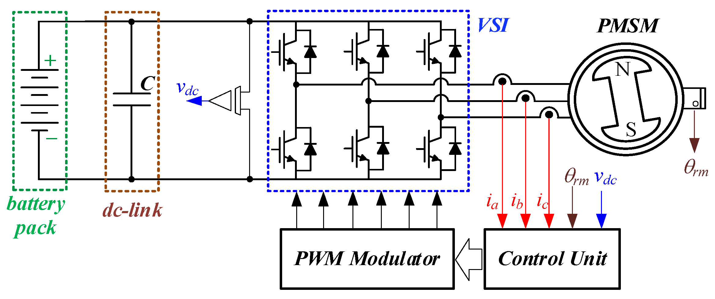
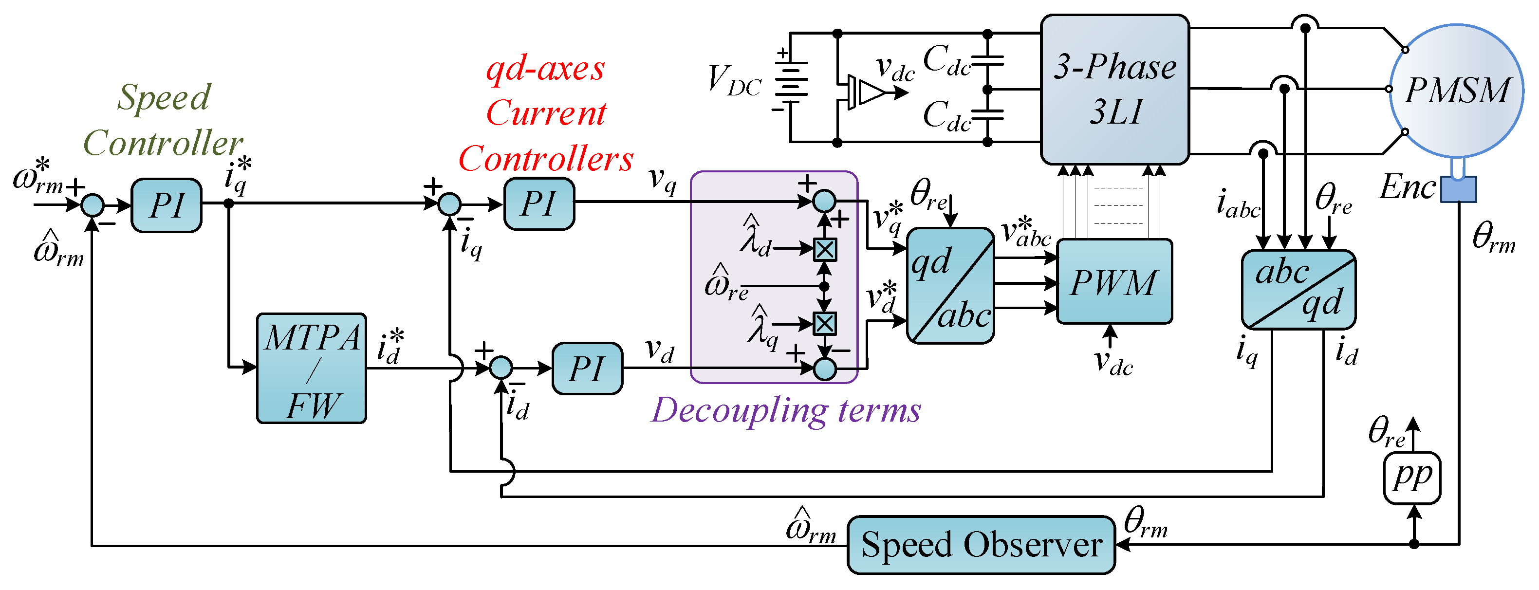
2. Electric Traction Drive Description

The traction drive under examination in this study comprises a DC battery pack, represented as a constant voltage source VDC, which is linked to one of the considered 3LIs. These inverters are responsible for powering the PMSM, employing a rotor flux field-oriented control strategy, enabling an independent control of torque and flux by appropriately managing the two qd-axes stator current components: iq and id. This is achieved through a closed current loop, as depicted in Figure 2. Field orientation is possible thanks to the suitable reference frame transformations abc/qd and qd/abc indicated in the same figure and in the modelling of the electrical machine. An external speed loop has been used to map the overall torque-speed operating range of the traction drive. Concerning the id current, its selection aims to minimize motor drive losses by employing established current vector profiles associated with the conditions of MTPA and FW.
Specifications of the interior permanent magnet synchronous motor (IPM) used for the considered traction drive are listed in Table 2, while motor parameters are presented in Table 3 [31].
The PMSM has been mathematically modelled in a qd-axes synchronous reference frame aligned with the rotor flux position θre [32,33], including iron losses, Figure 3. The equivalent iron loss resistance Rc is determined by accounting for hysteresis and eddy current losses, and is further expressed as a function of the rotational frequency ωre [34].
The PMSM model is described using Equations (1)–(4), encompassing both electrical and mechanical equations that govern the behavior of the electromechanical system [35]. Specifically, the qd-axes air-gap current components ioq and iod are determined starting from the voltage and current relationships (1), where Rs is the stator resistance, Rc is the equivalent iron loss resistance, Lq and Ld are the qd-axes inductances, λpm is the permanent magnet flux linkage, p denotes time derivative d/dt, vq and vd are the qd-axes voltage components, and voq, vod are the qd-axes air-gap voltage components, defined in (2). Meanwhile, icq and icd are the qd-axes iron losses’ current components and iq and id are the qd-axes input current components, both defined in (3). The electromagnetic torque Te and the mechanical equation of motion for the PMSM are provided by (4). Here, J represents the mechanical inertia, ωrm stands for the mechanical rotor speed, TL is mechanical torque load, and B denotes the viscous friction coefficient. The electrical rotor speed ωre is obtained as ωre = ppωrm, where pp are the pole pairs. The rotor position θrm is determined by integrating the rotor speed ωrm, as illustrated in Equation (4).
v q v d = R s i o q i o d + R c + R s R c v o q v o d v o q v o d = p L q ω r e L d ω r e L q p L d i o q i o d + ω r e λ p m 0
v o q = R c R c + R s ( v q R s i o q )   v o d = R c R c + R s ( v d R s   i o d )
i c q = v o q R c   i c d = v o d R c   i q = i c q + i o q   i d = i c d + i o d
T e = 3 2   p p [ λ p m i o q + ( L d L q ) i o d i o q ]   T e = T L + J   d ω r m d t + B ω r m   ω r m = d θ r m d t   ω r e = p p ω r m
The PMSM is powered by one of the three-phase 3LI configurations: ANPC, NPC, and TNPC. To supply the electric drive’s rated voltage at the rated speed, a DC bus voltage ranging 800 V is necessary. A single inverter leg of the NPC topology consists of 4 switches and 2 diodes per phase [36], Figure 4a. Conversely, the inverter leg of an ANPC substitutes the 2 diodes with two power switches [22], Figure 4b. As indicated by their names, both topologies clamp the midpoint of the capacitor to the neutral using diodes or switching devices. However, the NPC topology’s primary drawback involves the need for a balancing circuit to maintain voltage equilibrium across the capacitors. On the other hand, the ANPC topology does not require this additional circuitry but necessitates extra components to control the switches clamping the neutral [37]. The conventional inverter leg of a T-type inverter [38] consists of two power devices in the main inverter leg and inserting two back-to-back switching devices between the output-inverter node and the neutral point of the DC link created by the bulk input capacitors. However, the voltage stress on the devices composing the main leg is VDC, while that at the terminals of the back-to-back switching devices is VDC/2. Consequently, for the considered application the topology is modified by including four devices in the main inverter leg, as depicted in Figure 4c. This modification in the analyzed TNPC implements the serialization of power switches [39,40], posing challenges related to the simultaneous operation of devices functioning as a single switch. This challenge arises because individual switching devices might have differing turn-on and turn-off characteristics, necessitating an appropriate switching strategy for the efficient operation of both devices.
One significant advantage of employing 3LI topologies is the available array of modulating strategies [41,42]. In this study, the level shifted PWM modulation technique is utilized across all three topologies [41]. Throughout each commutation cycle, the output voltage alternates between +VDC/2, 0, and −VDC/2. The voltage across the terminals of each GaN power MOSFET in these topologies is VDC/2, offering a significant advantage, as the selected switching devices can be rated at half of the DC Bus Voltage. The modulation techniques employed for each topology are illustrated in Figure 5.
The realization of three-phase topologies involves adding two additional legs for the remaining two phases. The modulation strategies encompass two additional reference voltages phase shifted with 2π/3 and 4π/3 to synthesize a symmetrical voltage set [37,38,39,40].
The modeling described above has been implemented within the PSIM simulation platform, specifically tailored for simulating power-conversion systems and control algorithms. However, a major limitation of this approach arises due to substantial differences between the extremely rapid switching transients of GaN power MOSFETs and the dynamic response of the electrical machine. Consequently, if the objective is to assess the power loss distribution of the inverter’s power devices, simulating the entire drive will demand a considerable computational load and result in a prolonged time to achieve the steady-state condition in the simulated drive.
The aforementioned consideration has prompted the authors to devise an alternative methodology aimed at modeling the entire traction drive. In this approach, the power converters are implemented using ideal switches, while their conduction and switching power losses are determined using appropriate analytical models. Additionally, as the primary objective is to identify the power loss distribution among the GaN devices, the electrical machine is emulated with an equivalent three-phase RL load for each operating condition of the traction drive. By modelling the overall traction drive in this way, there is a substantial reduction in the computational load required for simulation, while maintaining a satisfactory level of accuracy in estimating 3LI power loss distribution. The efficacy of this approach is supported by the results outlined in the subsequent sections, which delve into the analysis of a 110 kW traction drive as a case study.

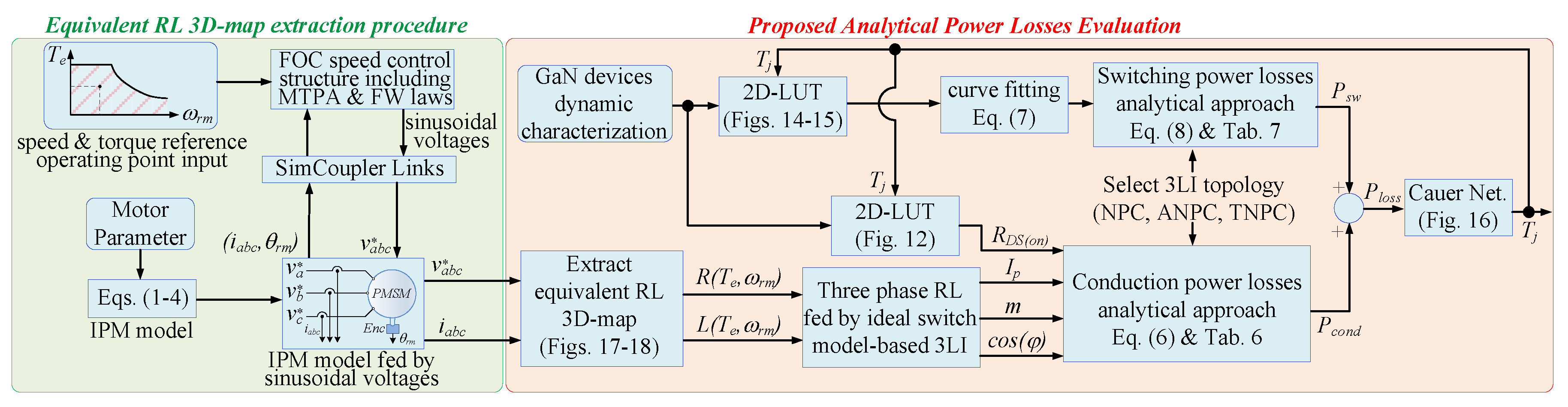
3. Methodology for the Estimation of Power Loss Distribution in GaN-Based 3LI

In this section, the authors describe the procedure that has been implemented to estimate the power loss distribution in the considered 3LIs. The first step is provided using the characterization of the GaN technology power devices in order to quantify the power losses of each power switch composing the inverter. The GaN semiconductor characterization is crucial to realize accurate analytical modelling of the power switch to consider both static and dynamic behaviors, and thus allowing to properly evaluate the switching and conduction losses of power devices in a wide range of operations. The characterization procedure has been applied to an early-stage GaN technology power device.

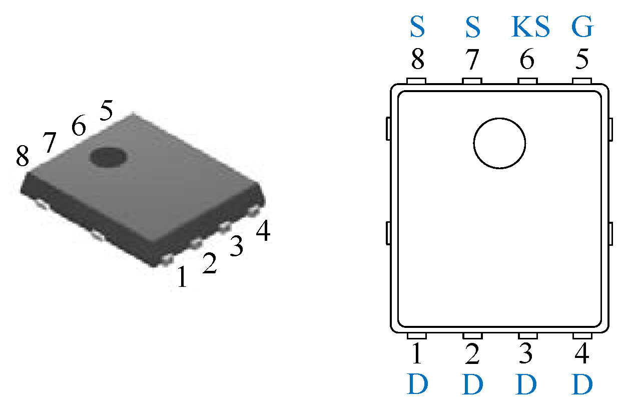
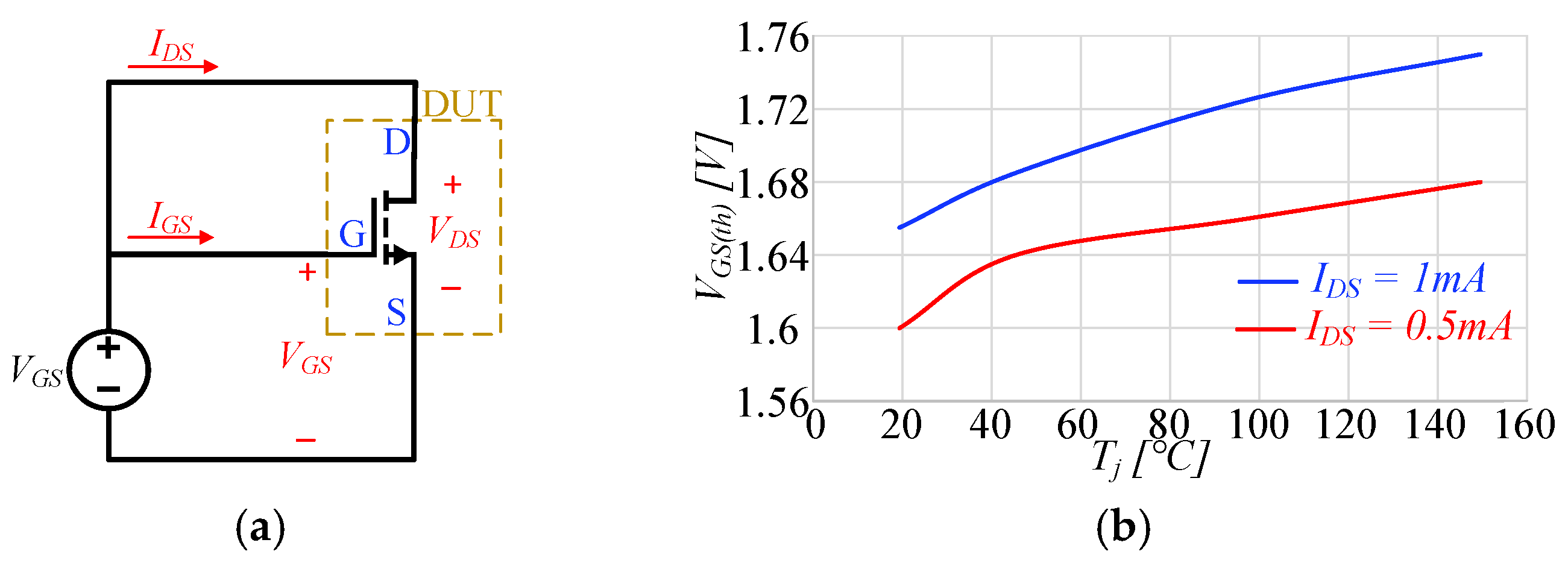
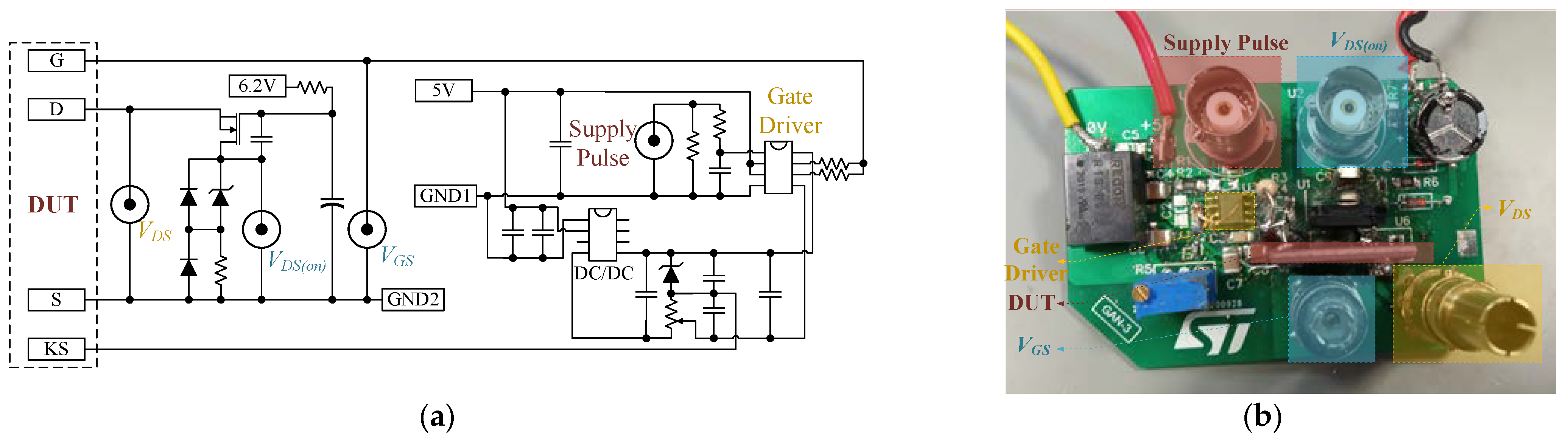
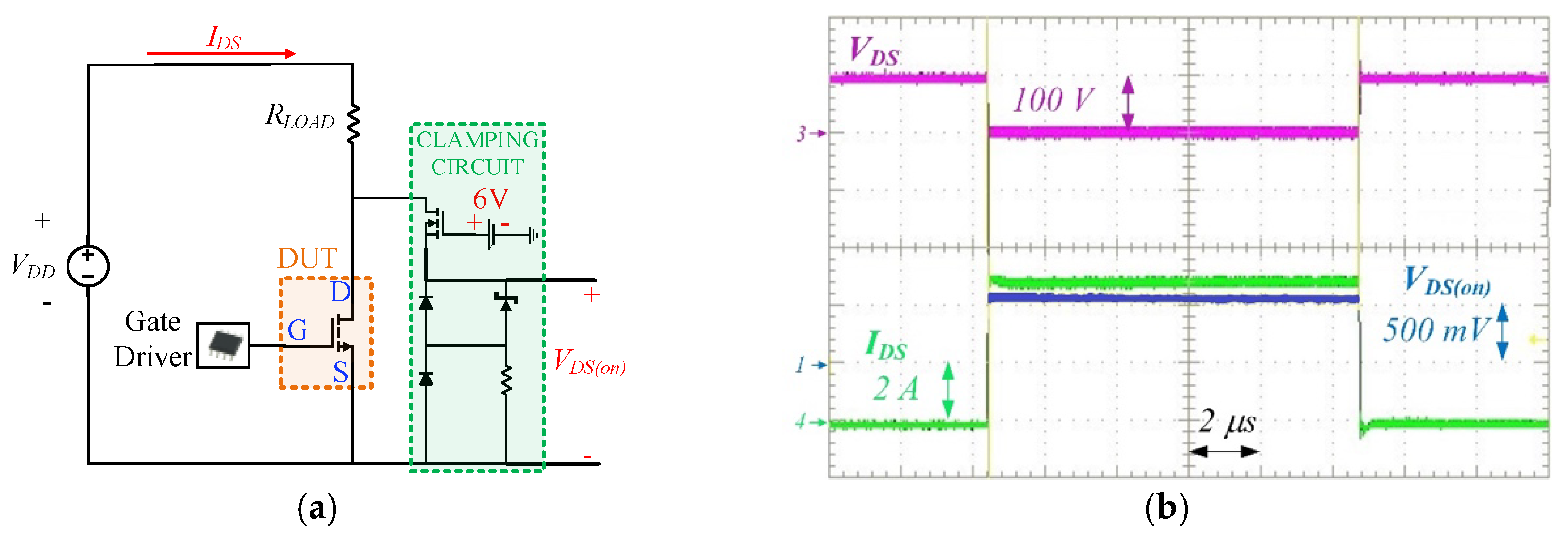
3.1. Characterization of GaN MOSFETs

To accurately assess inverter performance, power-device-parameter evaluation is essential. The SGT120R65AES, a prototype manufactured by STMicroelectronics, is the GaN power device being evaluated in this study. This transistor uses a PowerFLAT 5 × 6 package, shown in Figure 6, with a separate Kelvin source and source terminals to isolate the driving loop from the power loop, improving package parasitics. Table 4 presents the primary specifications of the analyzed GaN MOSFET.
The GaN device’s performance is evaluated based on switching and conduction losses. Hard-switching transients cause energy loss due to parasitic capacitances charging and discharging currents, while conduction losses depend on RDS(on). Proper evaluation of these quantities requires static and dynamic characterization tests, the outcomes of which are typically provided in power MOSFET datasheets. However, during the initial phases of technology development this information is lacking, thereby requiring a comprehensive characterization to be carried out. This becomes a critical concern, especially when integrating these GaN devices across multiple dies connected in parallel to form power modules.

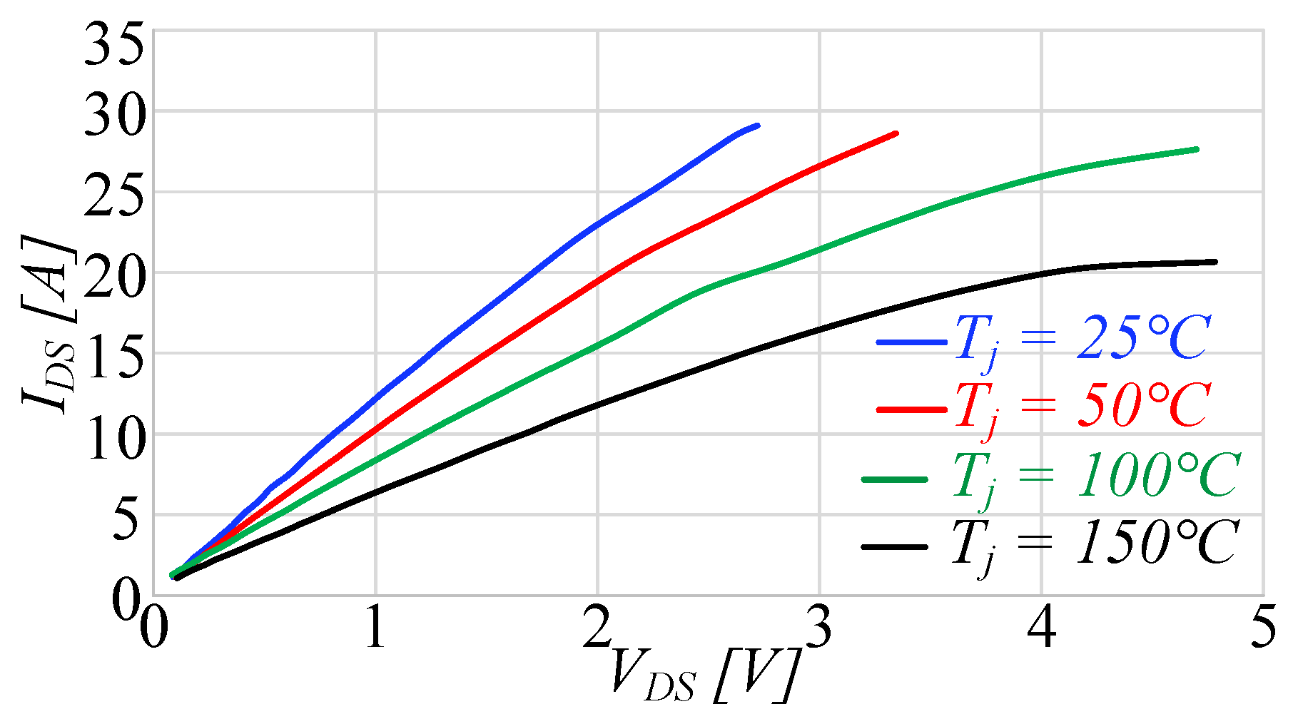
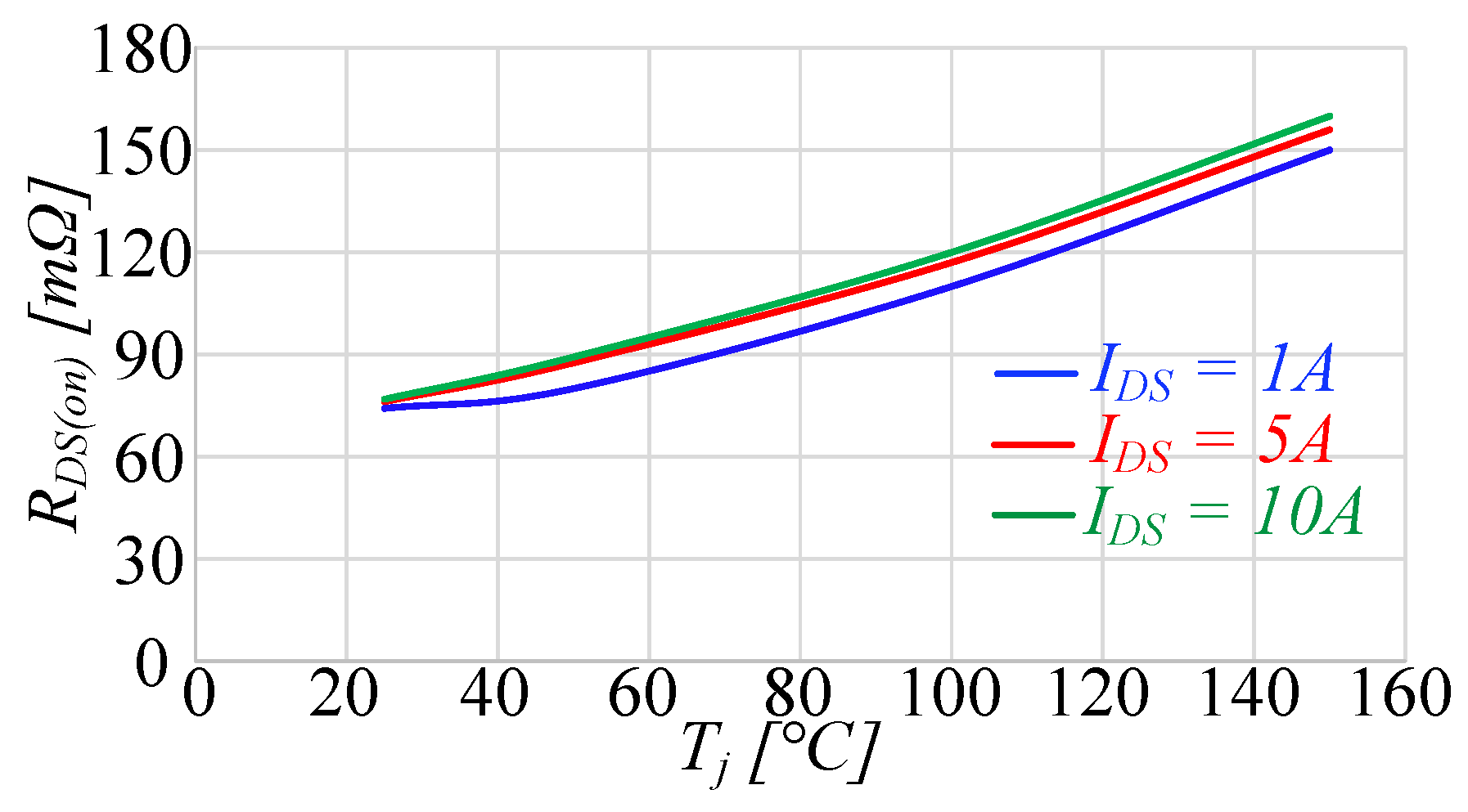
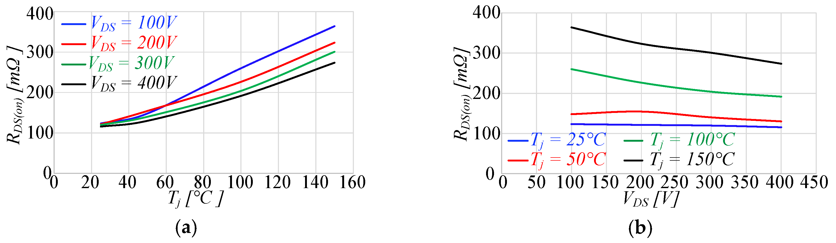
3.1.1. Static Characterization

Two curve tracers are used for static-power-device characterization: the Tektronix 370B for threshold gate-to-source voltage VGS(th) and the Tektronix 371A for static RDS(on) and output v-i characteristics. The 370B provides high-resolution measurements and the capability to set the very low current value (about 10–100 μA) necessary for VGS(th) tests, while the 371A enables high-voltage and high-current sourcing. To measure VGS(th) using the 370B, the drain and gate terminals are shortened to ensure identical current flow (IDS = IGS), as shown in Figure 7a.
The GaN transistor conducts when a 2DEG is created between the AlGaN and GaN layers through the piezoelectric effect [43]. The voltage at which device conduction begins is determined by varying the IDS current at 500 µA and 1 mA across temperatures from 25 °C to 150 °C, as shown in Figure 7b. Assuming the more stable threshold voltage indication at IDS = 1 mA, it increases with temperature from 1.65 V to 1.75 V.
The 371A Curve Tracer was used to establish the output characteristics of the considered GaN MOSFETs. This involves setting a specified VGS and incrementally increasing VDS to obtain the v-i characteristics for that VGS. The output characteristics are also evaluated while varying the junction temperature (Tj), as shown in Figure 8.
The static assessment of the RDS(on) of the analyzed GaN HEMTs is conducted using the Tektronix 371A Curve Tracer. RDS(on) can be determined from the curve tracer as a ratio of VDS(on) to IDS at specific value of VGS. Figure 9 shows the evaluation of the RDS(on) as function of the junction temperature from 25 °C to 150 °C, for three different values of IDS, at VGS = 6 V.
Threshold voltage, output characteristics, and RDS(on) profiles are the main static parameters necessary to implement the proposed model.

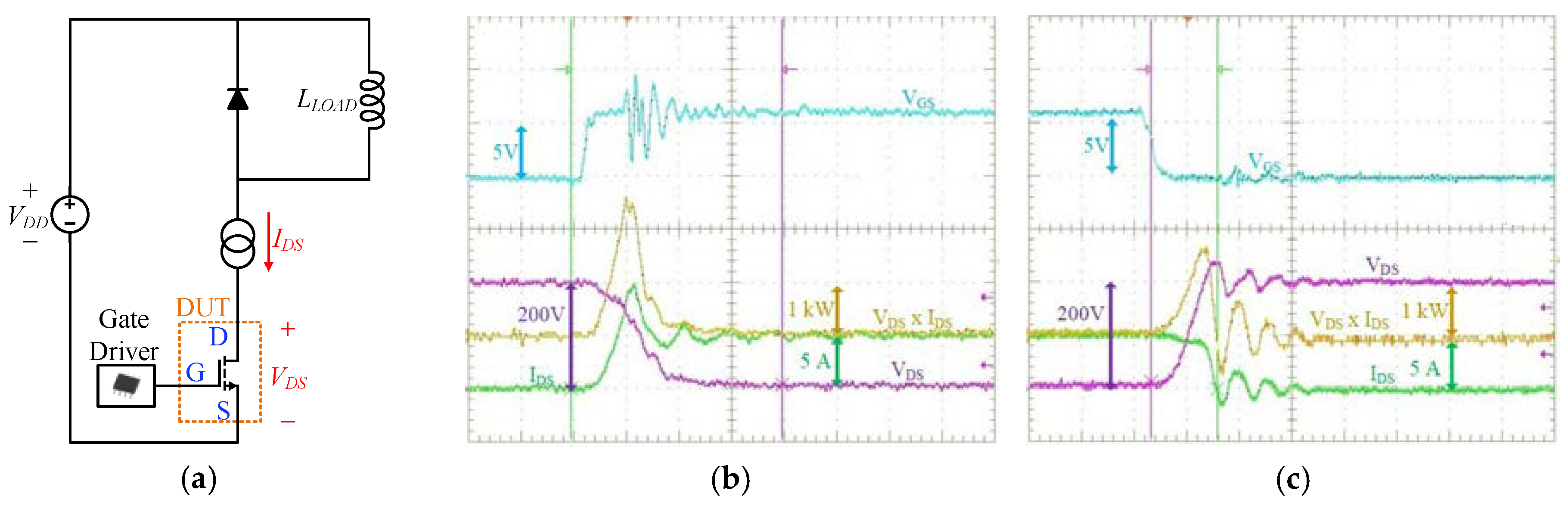
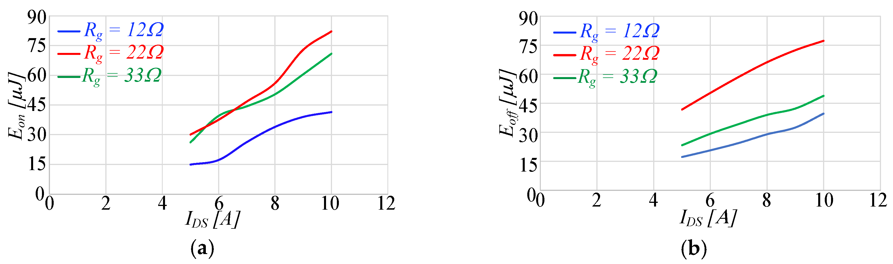
3.1.2. Dynamic Characterization

Dynamic characterization aims to assess “dynamic” parameters of DUTs, which in this case are mainly dynamic on-resistance RDS(on) and switching losses (Eon and Eoff) using a specialized board shown in Figure 10 and the Tektronix TDS 5054 Oscilloscope with TPP0500B probes for data acquisition. The board minimizes parasitic inductance paths, while the higher probe bandwidth of 500 MHz allows to correctly capture all dynamic signal response without impacting on its slew rate.
Dynamic RDS(on) issues are well-know research topics for GaN devices and more information can be found in the literature [44,45], while in this section we provide a more detailed description of its experimental evaluation for its inclusion in the proposed model.
The assessment of dynamic RDS(on) relies on the ratio of measured VDS(on) and IDS. However, a standard voltage probe lacks the sensitivity required to measure VDS(on), which falls within the millivolt range during the GaN HEMT’s turn-on phase, starting the transformation from VDD, that for the device under testing has a typical value of one hundred volts. Consequently, a voltage-clamping circuit has been implemented to clamp the voltage VDS(on) when the DUT is off, enabling the measurement of the actual VDS(on) during the device’s turn-on phase [44]. By concurrently measuring the current flowing through the device using a current probe and VDS(on), it becomes feasible to determine the RDS(on). Figure 11 illustrates the electric scheme of the test bench and typical waveforms of a measurement of VDS(on) (blue trace) and IDS (green trace) for the determination of the dynamic RDS(on).
Measurements of dynamic RDS(on) have been conducted considering a switching commutation on a resistive load applying a fixed number of pulses, typically 100, as a function of VDD from 100 V to 400 V and a case temperature from 25 °C and 150 °C. Due to the relationship between the time and application of the stressing voltage, it is necessary to evaluate the dynamic RDS(on) at different time instances, and example results for 400 V, 5 A at 25 °C are reported in Table 5.
From Table 5, it is apparent that RDS(on) decreases and stabilizes at a constant value over time. The relationship between RDS(on) variations concerning changes in temperature Tj and VDS is depicted in the results of Figure 12, confirming an increase in RDS(on) corresponding to the blocking time of the bus voltage [45]. Look up tables (LUTs) representative of RDS(on) variations with temperature and drain-to-source voltage have been realized and used in the proposed modelling.
Another significant source of losses occurring in the power devices is attributed to the commutations. These can be identified by implementing classical double-pulse tests. The circuit and the related switching energy loss estimation are shown in Figure 13.
The estimation of Eon and Eoff is conducted at the rated voltage VDD = 400 V while varying the current from 5 A to 10 A. The assessment involves varying parameters: Rg is modified while maintaining a constant case temperature Tcase, Figure 14, and case temperature is modified while keeping the gate resistance Rg constant, Figure 15.
The switching losses are recorded also with respect to the change in temperature from 25 °C to 150 °C. An increase in the trend of the losses is observed due to the higher rise time of the voltage and the current at higher junction temperatures. LUTs linking switching energy losses to IDS and Tj have also been developed to be integrated into the PSIM GaN power MOSFET model.
The GaN HEMTs have been modelled in PSIM using a MOSFET model including all results achieved using the static and dynamic characterization: the variations of RDS(on) in the forward and reverse conduction modes and energy losses Eon and Eoff. Drain-to-source voltage and current flowing through the MOSFET model are obtained from the simulation for each instance. These values are then used for the loss calculation. However, the value of RDS(on) is updated at each time step of the simulation.

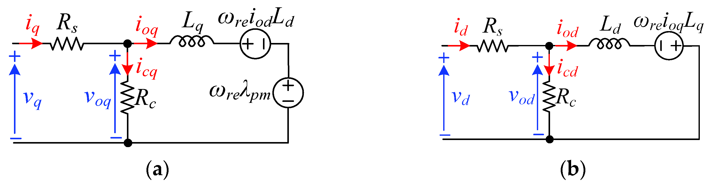
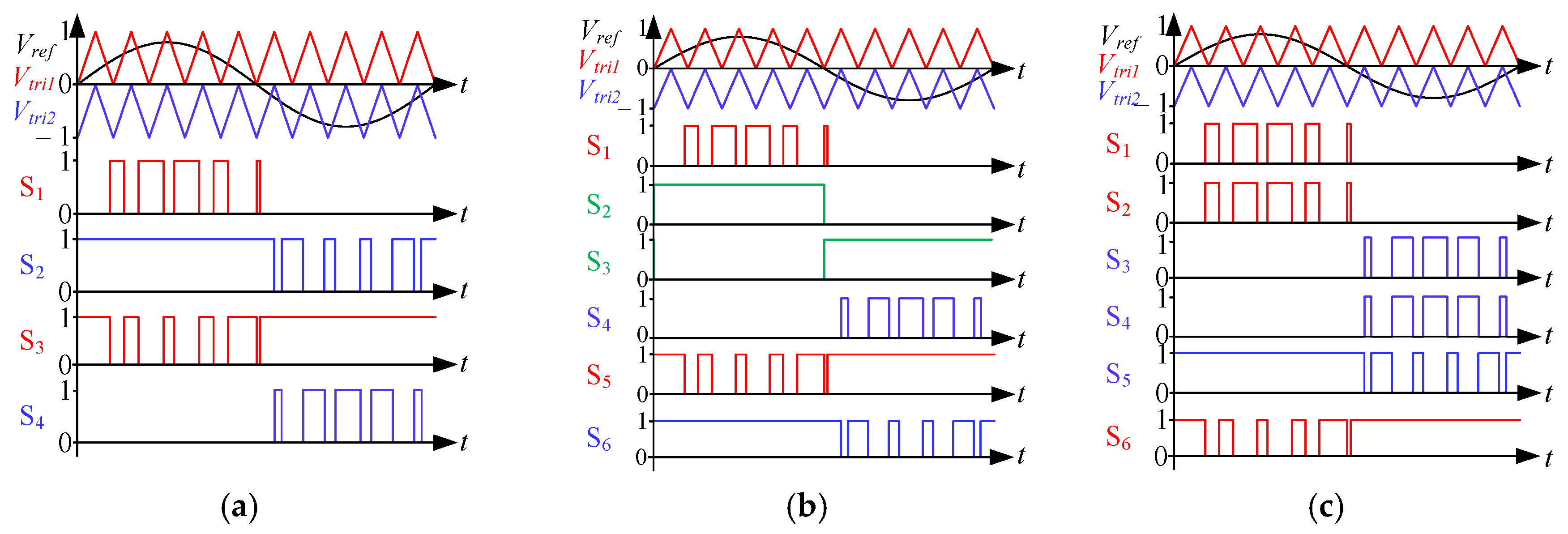
3.2. Analytical Power Loss Modelling of Three-Level Inverters

An alternative and effective approach to simulate the performance of the 3LI is the proposed one, which involves utilizing power converters composed of ideal switches and exploiting analytical models to estimate power losses and approximating the electrical machine with an equivalent RL load for various torque-speed operating conditions of the traction drive.
For each GaN power device composing the 3LI of the conduction losses Pcond are computed according to (5), where the root-mean-square (RMS) current is provided using (6); In this, we are assuming a sinusoidal single-phase load current I ( θ r e ) = I p   s i n ( θ r e φ ) , and the duty cycle δ(θre) of one phase of the PWM voltage waveform is defined as a quantity variable with the modulation index m and power factor cos(φ) [37,38,39,40,41,42,43,44,45,46,47,48]. The load current is identified using the peak value Ip and phase angle φ, while the angular position θre is provided using ωret, where ωre is the angular frequency of the fundamental voltage harmonic. RDS(on) is provided using the LUTs determined in the characterization phase.
P c o n d = R D S ( o n ) I 2 r m s
I r m s = 1 2 π   0 2 π I 2 ( θ r e )   δ ( θ r e ) d θ r e   = 1 2 π   0 2 π I 2 p sin 2 ( θ r e φ )   δ ( θ r e ) d θ r e
The carrier-based modulation techniques feature symmetrical behavior: Irms(S1) = Irms(S4), Irms(S2) = Irms(S3), Irms(S5) = Irms(S6), thus the conduction loss computation is limited to the top half of GaN devices of the power converter, i.e., S1, S2 and S5, whereas in the case of NPC topology D1 is symmetric to D2. The computation of the RMS currents Irms (6) for each device are reported in Table 6. The computation has been carried out considering the reverse-conduction mechanism of GaN HEMT, thus considering the two current parallel paths for each device. The state of the generic jth power switch Sj associated with forward and reverse current conductions is indicated with SjF and SjR, respectively. The same approach can be extended even to other modulation strategies, such as the third harmonic injection PWM techniques.
The switching losses were analytically calculated, starting from the measured Eon and Eoff, and determined from device characterization, which can be defined as the function of VDD, IDS and Rg. Under the assumption that VDS = 400 V and Rg = 10 Ω maintain constant values, the switching energies can be exclusively expressed as functions of IDS, (7). Their behavior can be depicted using a generic curve-fitting mathematical tool, where the weight coefficients k1, k2, k3 and k4 have been determined at different junction temperatures of Tj. For the considered GaNs, the energy loss profiles are provided using:
E o n = k 1 · 10 6   I D S k 2   E o f f = k 3 · 10 6   I D S k 4
The expression of the average switching power losses PSW(on) and PSW(off) over a fundamental period Tre = /ωre are provided in (8), where n is the ratio between switching fSW and fundamental fre = 1/Tre frequencies, equivalent to the number of commutations per fundamental period of the current, while n1 and n2 define the starting and final intervals in which each power device is PWM commutated. Starting from (7), the switching losses for each GaN device composing the 3LI can be expressed as a function of the output-load current characteristics, in terms of peak value Ip and phase angle φ. Their expression for the considered GaNs is as follows:
P S W ( o n ) = 1 n k = n 1 n 2 k 1 · 10 6   f S W   I p   s i n k ω r e f S W φ k 2         P S W ( o f f ) = 1 n k = n 1 n 2 k 3 · 10 6   f S W   I p   s i n k ω r e f S W φ k 4
Table 7 provides the values of n1 and n2 associated with each device used in the considered topologies.
In the calculation of these switching losses, symmetry is considered for the switches, similar to how RMS currents are computed. Based on the modulation strategy employed in the ANPC, the switching loss power associated with S2 and S3 is deemed negligible compared to the other switches within the 3LI configuration. This is due to their lower number of commutations in the fundamental period.
Furthermore, the proposed methodology also includes the estimation of the junction temperature Tj of the GaN HEMTs, updating the 2D-LUT outputs carried out from the static and dynamic characterizations for assessing conduction and switching losses. The determination of the junction temperature is conducted through the implementation of a thermal model. In this paper, a thermal model is realized with the 4th-order Cauer network shown in Figure 16. Network parameters are provided in Table 8, and Plosses = Pcond + Psw is the total loss profile, and the sum of the conduction and switching losses, which is modelled as a current source and the ambient temperature Tamb is provided using a voltage source. Between case and ambient temperature, a heatsink thermal impedance Rheatsink = 0.11 °C/W was included.
To streamline the modeling process, an adaptive RL network is used to represent the electrical equivalent circuit of the AC motor. The network’s values are chosen to be representative of the stator current for each operating torque-speed of the PMSM. The determination of both R and L parameter surfaces can be accomplished by conducting a series of simulations. These simulations involve supplying the controlled PMSM with sinusoidal voltages across the entire torque-speed map. This process is notably swift since it neglects the dynamics of the power converters, resulting in a significantly reduced execution time. The surfaces of the RL network for the considered PMSM are displayed in Figure 17 and Figure 18.
The proposed step-by-step procedure to evaluate the power losses for the three considered GaN-based 3LI topologies, have been displayed in Figure 19 and summarized below:
(1)
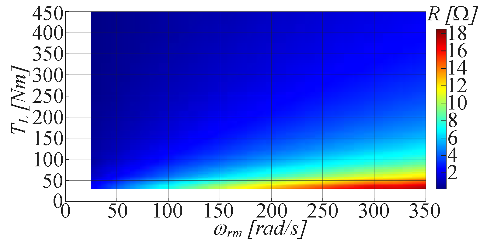
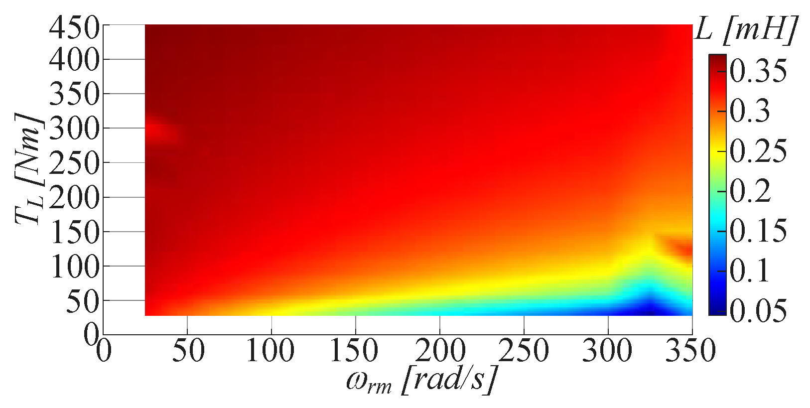
Initially, starting from the traction drive specifications, the IPM motor is modelled according to (1)–(4) and fed with sinusoidal voltage sets, corresponding to the several operating conditions (TL, ωrm). From the motor voltages and currents the R and L maps are carried out.
(2)
Then, according to the considered 3LIs topologies and modulation strategies, the command signals are applied to ideal switches composing the inverter which supplies the motor modelled as in (1)–(4).
(3)
For each working condition, the conduction and switching losses are computed according to (6)–(8).
(4)
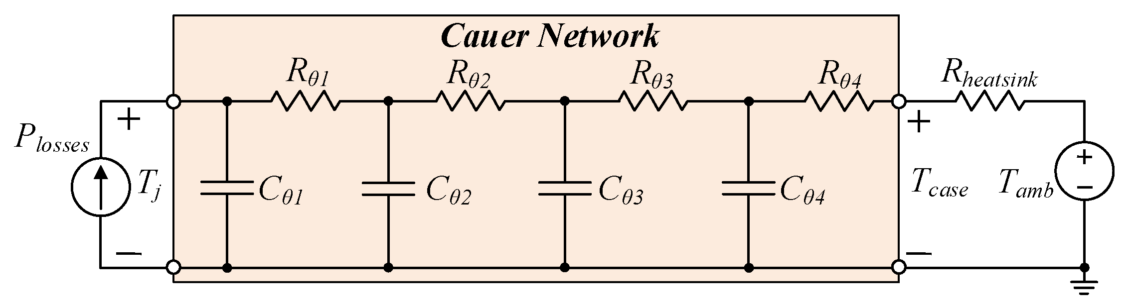
Cauer network is exploited to update the inputs data of the LUTs, and thus the parameters determined in the GaN HEMT characterization.

4. GaN-Based Traction Drive Modelling in PSIM

To verify the effectiveness of the proposed analytical power loss modelling of power converters, the traction drive was entirely implemented in PSIM, including the model of GaN HEMTs, which was determined according to the above-mentioned measurements, and the model of the IPM motor, Figure 20. To achieve the necessary current capability, it is assumed that you must connect 20 dies in parallel. Whereas a standard FOC speed and current control structures including MTPA, FW, speed observer, and the level shifted PWM have been implemented in Matlab/Simulink. Specifically, the SimCoupler block ensures the connection between the Matlab/Simulink control structure and the PSIM model. The gate signals are provided as PSIM inputs to drive the devices composing the 3LI topologies implemented in PSIM. The motor currents iabc and the mechanical rotor position θrm are PSIM outputs, serving as feedback for the speed and current control loops.
The considered 3LI inverters have been realized in PSIM as shown in Figure 21. Moreover, the aforementioned Cauer network has been integrated in the GaN devices of PSIM MOSFET models to estimate their heat dissipation.

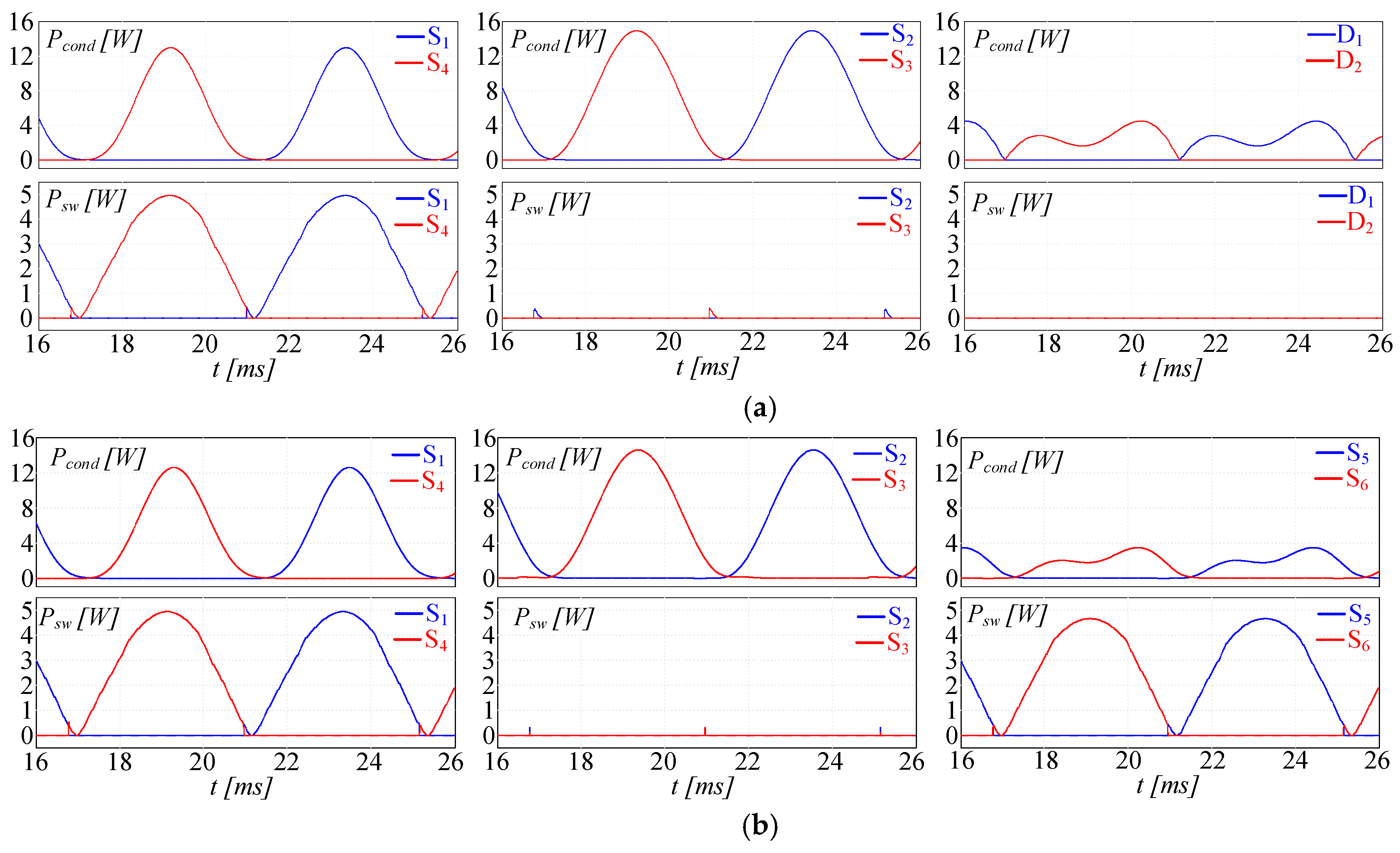
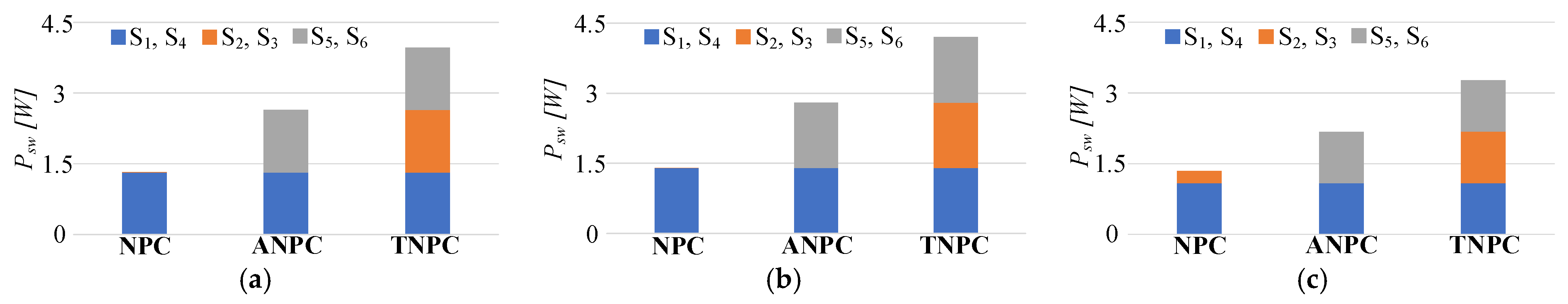
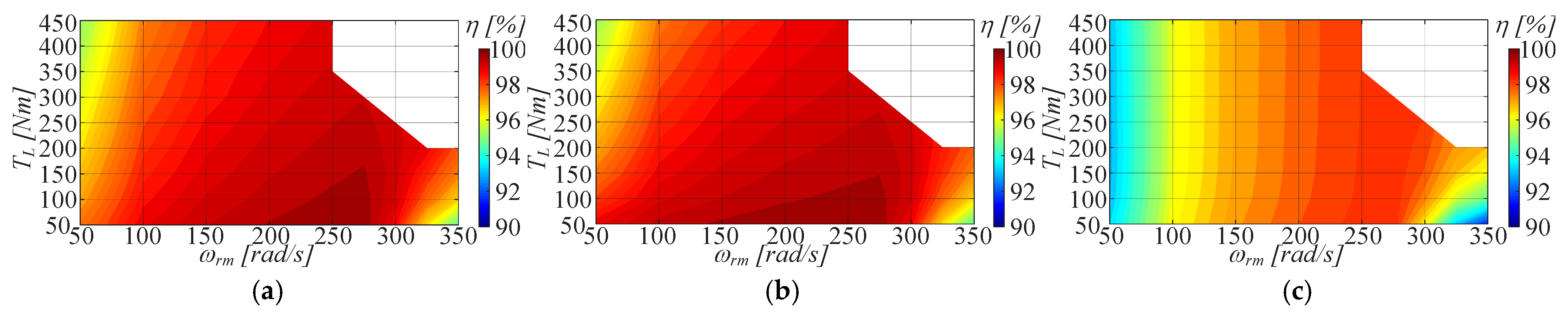
5. Analysis of Power Losses in the Case Study

The 110 kW traction drive considered in this study has been simulated using the two-modelling presented in the above sections. The power loss profiles for each GaN device and for the three considered 3LI topologies have been calculated by averaging each switching period and the profile of power loss distribution. Results are illustrated in Figure 22. It is worth noting that conduction and switching losses take place within a portion of the fundamental period. Moreover, the switching losses are quite limited for some power switches due to their specific switching pattern.
Figure 23 and Figure 24 illustrate the averaged conduction and switching power losses over a fundamental period for a single die, while considering three different motor drive operating points. It can be observed that unequal loss distribution occurs among GaN devices, for all 3LIs. Moreover, the conduction losses result is higher than the switching one because of the high value of RDS(on).
Similarly, Figure 25 summarizes the overall semiconductor losses, taking into account the same three motor drive operating points.
Based on the power loss analysis, it is possible to generate efficiency maps for the three considered inverters, the results of which are depicted in Figure 26.
According to the above results, the 3LI topologies utilizing GaN technology exhibit high performance owing to their notably low switching losses. However, the efficiency declines at low speeds and high torque levels due to conduction losses. Furthermore, efficiency above the rated speed diminishes due to an elevated d-axis current in the flux weakening region. Comparing the ANPC and NPC topologies, their efficiencies are nearly equivalent, with the ANPC offering slightly higher efficiency in the low-speed region. On the contrary, the TNPC demonstrates significantly lower efficiency compared to the other two topologies. This discrepancy is attributed to the series connection of GaN devices in the main leg, leading to increased overall conduction losses.
The power loss evaluation of the 3LIs using the combined mathematical modelling of converter power loss and the RL loads to simulate the electric traction drive offers a time-saving and efficient approach. However, in real-world scenarios, the impact of high-frequency components also needs consideration. Therefore, a comparison of the losses achieved by considering the overall drive, incorporating the inverter along with the effects of high-frequency components, against that estimated by the proposed approach has been conducted. This discrepancy is visually presented in Figure 27.
The higher error percentage is noticeable primarily at low load torque, specifically at low currents, attributed to the presence of high-frequency components. However, it is noteworthy that the error remains consistently below 2% at higher currents.
A comparison between the computational burdens associated with simulating the entire traction drive—encompassing both inverter and electrical machine dynamics—and the one achieved using the proposed approach has been conducted for various operating conditions. In both cases, the simulation stop time has been set at 1s, while the execution time has been set at 0.1ns. In particular, both simulations have been conducted with a reference speed of ωrmR and varying the torque load with a step at 0.5s from no-load to rated torque load conditions. The results are summarized in Table 9, illustrating a notable and substantial reduction in simulation time with the proposed solution, about 68%, independent of the 3LI topology considered.

6. Conclusions

The main key points to highlight in this work can be summarized as follows:
  • The proposed analytical power loss modeling, combined with an equivalent representation of the electrical machine yields accurate results across a wide range of traction drive operating conditions. This is evident from the comparison shown in Figure 27.
  • Moreover, this modelling proved to offer a viable solution capable of significantly reducing simulation times and computational load compared to a traditional approach, as clearly confirmed with the results summarized in Table 9.
  • Additionally, this methodology holds potential for extension to encompass various other topologies and modulation strategies, representing a promising area for future research activity.

Author Contributions

Conceptualization, A.S. and G.S.; methodology, G.S.; software, A.S., A.D.C. and L.D.T.; validation, A.S., M.P., L.S. and A.G.S.; formal analysis, A.S., A.D.C., L.D.T., M.P. and G.S.; investigation, A.S., A.D.C. and L.D.T.; resources, A.D.C. and L.D.T.; data curation, M.P., L.S., A.G.S., G.S. and M.C.; writing-original draft preparation, A.S., A.D.C., L.D.T., M.P. and G.S.; writing-review and editing, A.D.C., L.D.T., M.P. and G.S.; supervision, G.S. All authors have read and agreed to the published version of the manuscript.

Funding

This research was received no external funding.

Data Availability Statement

The original contributions presented in the study are included in the article, further inquiries can be directed to the corresponding authors.

Conflicts of Interest

The authors declare no conflict of interest.

References

  1. Sathiyan, S.P.; Pratap, C.B.; Stonier, A.A.; Peter, G.; Sherine, A.; Praghash, K.; Ganji, V. Comprehensive Assessment of Electric Vehicle Development, Deployment, and Policy Initiatives to Reduce GHG Emissions: Opportunities and Challenges. IEEE Access 2022, 10, 53614–53639. [Google Scholar] [CrossRef]
  2. Barbosa, W.; Prado, T.; Batista, C.; Câmara, J.C.; Cerqueira, R.; Coelho, R.; Guarieiro, L. Electric Vehicles: Bibliometric Analysis of the Current State of the Art and Perspectives. Energies 2022, 15, 395. [Google Scholar] [CrossRef]
  3. Ali, I.; Naushad, M. A Study to Investigate What Tempts Consumers to Adopt Electric Vehicles. World Electr. Veh. J. 2022, 13, 26. [Google Scholar] [CrossRef]
  4. Tu, H.; Feng, H.; Srdic, S.; Lukic, S. Extreme Fast Charging of Electric Vehicles: A Technology Overview. IEEE Trans. Transp. Electrif. 2019, 5, 861–878. [Google Scholar] [CrossRef]
  5. Jahns, T.M.; Dai, H. The past, present, and future of power electronics integration technology in motor drives. CPSS Trans. Power Electron. Appl. 2017, 2, 197–216. [Google Scholar] [CrossRef]
  6. Goli, C.S.; Manjrekar, M.; Essakiappan, S.; Sahu, P.; Shah, N. Landscaping and Review of Traction Motors for Electric Vehicle Applications. In Proceedings of the 2021 IEEE Transportation Electrification Conference & Expo (ITEC), Chicago, IL, USA, 21–25 June 2021; pp. 162–168. [Google Scholar]
  7. Goli, C.S.; Essakiappan, S.; Sahu, P.; Manjrekar, M.; Shah, N. Review of Recent Trends in Design of Traction Inverters for Electric Vehicle Applications. In Proceedings of the 2021 IEEE 12th International Symposium on Power Electronics for Distributed Generation Systems (PEDG), Chicago, IL, USA, 28 June–1 July 2021; pp. 1–6. [Google Scholar]
  8. Aghabali, I.; Bauman, J.; Kollmeyer, P.J.; Wang, Y.; Bilgin, B.; Emadi, A. 800-V Electric Vehicle Powertrains: Review and Analysis of Benefits, Challenges, and Future Trends. IEEE Trans. Transp. Electrif. 2021, 7, 927–948. [Google Scholar] [CrossRef]
  9. Allca-Pekarovic, A.; Kollmeyer, P.J.; Mahvelatishamsabadi, P.; Mirfakhrai, T.; Naghshtabrizi, P.; Emadi, A. Comparison of IGBT and SiC Inverter Loss for 400V and 800V DC Bus Electric Vehicle Drivetrains. In Proceedings of the 2020 IEEE Energy Conversion Congress and Exposition (ECCE), Detroit, MI, USA, 11–15 October 2020; pp. 6338–6344. [Google Scholar]
  10. Reimers, J.; Dorn-Gomba, L.; Mak, C.; Emadi, A. Automotive Traction Inverters: Current Status and Future Trends. IEEE Trans. Veh. Technol. 2019, 68, 3337–3350. [Google Scholar] [CrossRef]
  11. Tang, Z.; Akin, B. Suppression of Dead-Time Distortion Through Revised Repetitive Controller in PMSM Drives. IEEE Trans. Energy Convers. 2017, 32, 918–930. [Google Scholar] [CrossRef]
  12. Dai, S.; Wang, J.; Sun, Z.; Chong, E. Deadbeat Predictive Current Control for High-Speed Permanent Magnet Synchronous Machine Drives With Low Switching-To-Fundamental Frequency Ratios. IEEE Trans. Ind. Electron. 2022, 69, 4510–4521. [Google Scholar] [CrossRef]
  13. Oliveira, A.C.; Jacobina, C.B.; Lima, A.M.N. Improved Dead-Time Compensation for Sinusoidal PWM Inverters Operating at High Switching Frequencies. IEEE Trans. Ind. Electron. 2007, 54, 2295–2304. [Google Scholar] [CrossRef]
  14. Lidow, A.; De Rooij, M.; Strydom, J.; Reusch, D.; Glaser, J. GaN Transistors for Efficient Power Conversion; John Wiley & Sons: Hoboken, NJ, USA, 2019. [Google Scholar]
  15. Millán, J.; Godignon, P.; Perpiñà, X.; Pérez-Tomás, A.; Rebollo, J. A Survey of Wide Bandgap Power Semiconductor Devices. IEEE Trans. Power Electron. 2014, 29, 2155–2163. [Google Scholar] [CrossRef]
  16. Morya, A.; Moosavi, M.; Gardner, M.C.; Toliyat, H.A. Applications of Wide Bandgap (WBG) devices in AC electric drives: A technology status review. In Proceedings of the 2017 IEEE International Electric Machines and Drives Conference (IEMDC), Miami, FL, USA, 21–24 May 2017; pp. 1–8. [Google Scholar]
  17. Yang, Y.; Dorn-Gomba, L.; Rodriguez, R.; Mak, C.; Emadi, A. Automotive Power Module Packaging: Current Status and Future Trends. IEEE Access 2020, 8, 160126–160144. [Google Scholar] [CrossRef]
  18. Foti, S.; Testa, A.; Scimone, T.; De Caro, S.; Tornello, L.D.; Scarcella, G.; Scelba, G. A novel Hybrid N-Level T-Type Inverter Topology. In Proceedings of the 2019 IEEE Energy Conversion Congress and Exposition (ECCE), Baltimore, MD, USA, 29 September–3 October 2019; pp. 5507–5513. [Google Scholar]
  19. Satpathy, S.; Bhattacharya, S.; Veliadis, V. Comprehensive Loss Analysis of Two-level and Three-Level Inverter for Electric Vehicle Using Drive Cycle Models. In Proceedings of the IECON 2020 The 46th Annual Conference of the IEEE Industrial Electronics Society, Singapore, 18–21 October 2020; pp. 2017–2024. [Google Scholar]
  20. Satpathy, S.; Das, P.P.; Bhattacharya, S.; Veliadis, V. Design Considerations of a GaN-based Three-Level Traction Inverter for Electric Vehicles. In Proceedings of the 2022 IEEE 9th Workshop on Wide Bandgap Power Devices & Applications (WiPDA), Redondo Beach, CA, USA, 7–9 November 2022; pp. 192–197. [Google Scholar]
  21. Barater, D.; Concari, C.; Buticchi, G.; Gurpinar, E.; De, D.; Castellazzi, A. Performance Evaluation of a Three-Level ANPC Photovoltaic Grid-Connected Inverter With 650-V SiC Devices and Optimized PWM. IEEE Trans. Ind. Appl. 2016, 52, 2475–2485. [Google Scholar] [CrossRef]
  22. Valente, M.; Iannuzzo, F.; Yang, Y.; Gurpinar, E. Performance Analysis of a Single-phase GaN-based 3L-ANPC Inverter for Photovoltaic Applications. In Proceedings of the 2018 IEEE 4th Southern Power Electronics Conference (SPEC), Singapore, 10–13 December 2018; pp. 1–8. [Google Scholar]
  23. Haitham, A.R.; Holtz, J.; Rodriguez, J.; Baoming, G. Medium volt-age multilevel converters-state of the art, challenges, and requirements in industrial applications. IEEE Trans. Ind. Electron. 2010, 57, 2581–2596. [Google Scholar]
  24. Liu, Y.; Bazzi, A.M. A comprehensive analytical power loss model of an induction motor drive system with loss minimization control. In Proceedings of the 2015 IEEE International Electric Machines & Drives Conference (IEMDC), Coeur d’Alene, ID, USA, 10–13 May 2015; pp. 1638–1643. [Google Scholar]
  25. Mapelli, F.L.; Tarsitano, D.; Mauri, M. Plug-In Hybrid Electric Vehicle: Modeling, Prototype Realization, and Inverter Losses Reduction Analysis. IEEE Trans. Ind. Electron. 2010, 57, 598–607. [Google Scholar] [CrossRef]
  26. Williamson, S.S.; Emadi, A.; Rajashekara, K. Comprehensive Efficiency Modeling of Electric Traction Motor Drives for Hybrid Electric Vehicle Propulsion Applications. IEEE Trans. Veh. Technol. 2007, 56, 1561–1572. [Google Scholar] [CrossRef]
  27. Aarniovuori, L.; Laurila, L.I.E.; Niemela, M.; Pyrhonen, J.J. Measurements and Simulations of DTC Voltage Source Converter and Induction Motor Losses. IEEE Trans. Ind. Electron. 2012, 59, 2277–2287. [Google Scholar] [CrossRef]
  28. Nemeth, T.; Bubert, A.; Becker, J.N.; De Doncker, R.W.; Sauer, D.U. A Simulation Platform for Optimization of Electric Vehicles With Modular Drivetrain Topologies. IEEE Trans. Transp. Electrif. 2018, 4, 888–900. [Google Scholar] [CrossRef]
  29. Stabile, A.; Estima, J.O.; Boccaletti, C.; Cardoso, A.J.M. Converter Power Loss Analysis in a Fault-Tolerant Permanent-Magnet Synchronous Motor Drive. IEEE Trans. Ind. Electron. 2015, 62, 1984–1996. [Google Scholar] [CrossRef]
  30. Zhang, D.; Cittanti, D.; Sun, P.; Huber, J.; Bojoi, R.I.; Kolar, J.W. Detailed Modeling and In-Situ Calorimetric Verification of Three-Phase Sparse NPC Converter Power Semiconductor Losses. IEEE J. Emerg. Sel. Top. Power Electron. 2023, 11, 3409–3423. [Google Scholar] [CrossRef]
  31. Choe, Y.Y.; Oh, S.Y.; Ham, S.H.; Jang, I.S.; Cho, S.Y.; Lee, J.; Ko, K.C. Comparison of concentrated and distributed winding in an IPMSM for vehicle traction. Energy Procedia 2012, 14, 1368–1373. [Google Scholar] [CrossRef]
  32. Hassan, W.; Wang, B. Efficiency optimization of PMSM based drive system. In Proceedings of the 7th International Power Electronics and Motion Control Conference, Harbin, China, 2–5 June 2012; Volume 2, pp. 1027–1033. [Google Scholar]
  33. Scelba, G.; Tornello, L.D.; Scarcella, G.; Cacciato, M.; Testa, A.; Foti, S.; Pulvirenti, M. Combined Rotor Position Estimation and Temperature Monitoring in Sensorless Synchronous Motor Drives. In Proceedings of the 2018 IEEE 9th International Symposium on Sensorless Control for Electrical Drives (SLED), Helsinki, Finland, 13–14 September 2018; pp. 30–35. [Google Scholar]
  34. Qu, Z.; Tuovinen, T.; Hinkkanen, M. Minimizing losses of a synchronous reluctance motor drive taking into account core losses and magnetic saturation. In Proceedings of the 2014 16th European Conference on Power Electronics and Applications, Lappeenranta, Finland, 26–28 August 2014; pp. 1–10. [Google Scholar]
  35. Cavallaro, C.; Di Tommaso, A.O.; Miceli, R.; Raciti, A.; Galluzzo, G.R.; Trapanese, M. Efficiency enhancement of permanent-magnet synchronous motor drives by online loss minimization approaches. IEEE Trans. Ind. Electron. 2005, 52, 1153–1160. [Google Scholar] [CrossRef]
  36. Gupta, K.K.; Bhatnagar, P. Multilevel Inverters: Conventional and Emerging Topologies and Their Control; Academic Press: Cambridge, MA, USA, 2017. [Google Scholar]
  37. Mita, S.; Sujeeth, A.; Aiello, G.; Patti, D.; Gennaro, F.; Scelba, G.; Cacciato, M. Power Loss Modelling of GaN HEMT-based 3L-ANPC Three-Phase Inverter for different PWM Techniques. In Proceedings of the 2022 24th European Conference on Power Electronics and Applications (EPE’22 ECCE Europe), Hanover, Germany, 5–9 September 2022; pp. P.1–P.10. [Google Scholar]
  38. Schweizer, M.; Kolar, J.W. Design and implementation of a highly efficient three-level T-type converter for low-voltage applications. IEEE Trans. Power Electron. 2012, 28, 899–907. [Google Scholar] [CrossRef]
  39. Jørgensen, A.B.; Sønderskov, S.H.; Beczkowski, S.; Bidoggia, B.; Munk-Nielsen, S. Analysis of cascaded silicon carbide MOSFETs using a single gate driver for medium voltage applications. IET Power Electron. 2020, 13, 413–419. [Google Scholar] [CrossRef]
  40. Roig, J.; Gomez, G.; Bauwens, F.; Vlachakis, B.; Rodriguez, J.; Rogina, M.R.; Rodriguez, A.; Lamar, D.G. Series-connected GaN transistors for ultra-fast high-voltage switch (>1kV). In Proceedings of the 2017 IEEE Applied Power Electronics Conference and Exposition (APEC), Tampa, FL, USA, 26–30 March 2017; pp. 3043–3048. [Google Scholar]
  41. Rodriguez, J.; Lai, J.S.; Peng, F.Z. Multilevel inverters: A survey of topologies, controls, and applications. IEEE Trans. Ind. Electron. 2002, 49, 724–738. [Google Scholar] [CrossRef]
  42. Testa, A.; Foti, S.; De Caro, S.; Tornello, L.D.; Scelba, G.; Scarcella, G. Optimal Selection of the Voltage Modulation Strategy for an Open Winding Multilevel Inverter. In Proceedings of the 2020 IEEE Energy Conversion Congress and Exposition (ECCE), Detroit, MI, USA, 11–15 October 2020; pp. 2231–2237. [Google Scholar]
  43. Yu, E.T.; Dang, X.Z.; Yu, L.S.; Qiao, D.; Asbeck, P.M.; Lau, S.S.; Sullivan, G.J.; Boutros, K.S.; Redwing, J.M. Piezoelectric enhancement of Schottky barrier heights in GaN-AlGaN HFET structures. In Proceedings of the 56th Annual Device Research Conference Digest (Cat. No. 98TH8373), Charlottesville, VA, USA, 22–24 June 1998; pp. 116–117. [Google Scholar]
  44. Gelagaev, R.; Jacqmaer, P.; Driesen, J. A Fast Voltage Clamp Circuit for the Accurate Measurement of the Dynamic ON-Resistance of Power Transistors. IEEE Trans. Ind. Electron. 2015, 62, 1241–1250. [Google Scholar] [CrossRef]
  45. Zulauf, G.; Guacci, M.; Kolar, J.W. Dynamic on-Resistance in GaN-on-Si HEMTs: Origins, Dependencies, and Future Characterization Frameworks. IEEE Trans. Power Electron. 2020, 35, 5581–5588. [Google Scholar] [CrossRef]
  46. Schulte, C.; Böcker, J. Co-simulation of an electric traction drive. In Proceedings of the 2013 International Electric Machines & Drives Conference, Chicago, IL, USA, 12–15 May 2013; pp. 974–978. [Google Scholar]
  47. Ballestín-Bernad, V.; Artal-Sevil, J.S.; Domínguez-Navarro, J.A. Co-Simulation of a Two-Phase Axial-Gap Transverse Flux Machine. In Proceedings of the 2022 International Conference on Electrical Machines (ICEM), Valencia, Spain, 5–8 September 2022; pp. 956–961. [Google Scholar]
  48. Turrisi, G.; Tornello, L.D.; Scelba, G.; Cacciato, M.; Scarcella, G. Losses Evaluation in Current Source Inverter Topologies for Automotive Traction Applications. In Proceedings of the 2023 25th European Conference on Power Electronics and Applications (EPE’23 ECCE Europe), Aalborg, Denmark, 4–8 September 2023; pp. 1–11. [Google Scholar]
Figure 1. Standard IGBT-based 2L VSI topology used in the automotive industry.
Energies 17 00595 g001
Figure 2. Closed-loop implementation of traction drive.
Energies 17 00595 g002
Figure 3. Dynamic equivalent circuit of the IPM machine: (a) q-axis and (b) d-axis.
Energies 17 00595 g003
Figure 4. Single inverter legs of the considered three-phase inverters: (a) NPC, (b) ANPC, and (c) TNPC.
Energies 17 00595 g004
Figure 5. Modulation schemes and corresponding switching patterns for the inverter legs composing the (a) NPC, (b) ANPC, and (c) TNPC.
Energies 17 00595 g005
Figure 6. SGT120R65AES GaN MOSFET.
Energies 17 00595 g006
Figure 7. (a) Test circuit used for the estimation of VGS(th) using the curve tracer, and (b) VGS(th) measured at different temperatures and currents IDS.
Energies 17 00595 g007
Figure 8. Output v-i characteristics at different junction temperature Tj and at VGS = 6 V.
Energies 17 00595 g008
Figure 9. Static RDS(on) at different junction temperatures Tj and IDS.
Energies 17 00595 g009
Figure 10. Characterization board used for the dynamic characterization of GaN HEMTs power devices: (a) schematics and (b) evaluation board.
Energies 17 00595 g010
Figure 11. (a) Test circuit used to measure the VDS(on). (b) Evaluation of VDS(on) at VDD = 100 V and IDS = 5 A.
Energies 17 00595 g011
Figure 12. (a) Measurement of RDS(on) at different VDS (b) Measurement of RDS(on) at different Tj.
Energies 17 00595 g012
Figure 13. Double-pulse tests: (a) electric scheme, (b) Eon estimation, and (c) Eoff estimation.
Energies 17 00595 g013
Figure 14. (a) on and (b) off switching energy losses evaluated at different IDS and Rg.
Energies 17 00595 g014
Figure 15. (a) on and (b) off switching energy losses with respect to change in the junction temperature.
Energies 17 00595 g015
Figure 16. Cauer thermal network utilized in the GaN HEMT model at Tamb = 25 °C.
Energies 17 00595 g016
Figure 17. Map of R vs. TL and ωrm.
Energies 17 00595 g017
Figure 18. Map of L vs. TL and ωrm.
Energies 17 00595 g018
Figure 19. Block diagram of the proposed analytical power losses modelling of 3LIs.
Energies 17 00595 g019
Figure 20. PSIM implementation of the PMSM drive: (a) Matlab coupled with IPM fed with 3LI topologies PSIM model, (b) block diagram of the traction drive power loss estimation.
Energies 17 00595 g020
Figure 21. PSIM implementations of 3LI topologies considered in this study: (a) NPC, (b) ANPC, and (c) TNP.
Energies 17 00595 g021
Figure 22. Profile of power loss distribution across the switches composing the three 3LIs legs, averaged in each switching period: (a) NPC, (b) ANPC, and (c) TNPC. The traction drive is operated at TL = 450 Nm and ωrm = 250 rad/s.
Energies 17 00595 g022aEnergies 17 00595 g022b
Figure 23. Distribution of conduction losses in the considered 3LI topologies, computed at the following operating conditions: (a) TL = 450 Nm and ωrm = 50 rad/s, (b) TL = 450 Nm and ωrm = 250 rad/s, and (c) TL = 150 Nm and ωrm = 350 rad/s.
Energies 17 00595 g023
Figure 24. Distribution of switching losses in the considered 3LI topologies, computed at the following operating conditions: (a) TL=450 Nm and ωrm = 50 rad/s, (b) TL = 450 Nm and ωrm = 250 rad/s, and (c) TL = 150 Nm and ωrm = 350 rad/s.
Energies 17 00595 g024
Figure 25. Overall losses in the considered 3LI topologies at the following operating conditions: (a) TL = 450 Nm and ωrm = 50 rad/s, (b) TL = 450 Nm and ωrm = 250 rad/s, and (c) TL = 150 Nm and ωrm = 350 rad/s.
Energies 17 00595 g025
Figure 26. Efficiency maps of the considered 3LIs: (a) NPC, (b) ANPC, and (c) TNPC.
Energies 17 00595 g026
Figure 27. Percentage error between the losses provided using the modelling of the overall traction drive and that estimated using the proposed modelling for (a) NPC, (b) ANPC and (c) TNPC.
Energies 17 00595 g027
Table 1. Material properties of Si, GaN, and SiC.
ParameterUnitSiGaNSiC
Band Gap (Eg)eV1.123.393.26
Critical Field (Ecrit)MV/cm0.233.32.2
Electron Mobility (µn)cm2/(V∙s)14001500950
Permittivity (ɛr) 11.899.7
Thermal Conductivity (λ)W/(cm∙K)1.51.33.8
Table 2. IPM traction drive.
ParameterValue
Maximum power110 kW
DC bus voltage (VDC)800 V
Switching frequency (fsw)50 kHz
Maximum torque @ rated speed450 Nm
Rated speed (ωrmR)250 rad/s
Maximum speed (ωrmax)350 rad/s
Table 3. IPM motor parameters.
ParameterSymbolValue
Stator resistanceRs18.3 mΩ
q-axis inductanceLq745 μH
d-axis inductanceLd361.4 μH
Permanent magnet fluxλpm0.45 Wb
Equivalent iron loss resistance @ ωrmRRc50 Ω
Table 4. Main specifications of SGT120R65AES.
ParameterValue
Drain-source blocking voltage (V(BL)DSS)650 V
Continuous drain current (IDS)15 A @ Tcase = 25 °C
12 A @ Tcase = 100 °C
Operating junction temperature (Tj)−50 °C to +150 °C
Table 5. Dynamic RDS(on) at VDS = 400 V and IDS = 5 A at Tj = 25 °C.
t [µs]2.557.510
RDS(on) [mΩ]121.3117.8115.5115.5
Table 6. Modulation functions and RMS currents across devices.
TopologyDeviceδ(θre)Irms
NPCS1F, S4F m   s i n ( θ r e )     φ < θ r e < π I p m   c o s ( φ ) + 1 2 / ( 6 π )
S1R, S4R m   s i n ( θ r e )     0 < θ r e < φ
I p m   c o s ( φ ) 1 2 / ( 6 π )
S2F, S3F1    φ < θ r e < π
1 + m   s i n ( θ r e )    π < θre < π + φ

I p 1 / 4 m   c o s ( φ ) 1 2 / ( 6 π ) )
S2R, S3R m   s i n ( θ r e )
I p m   c o s ( φ ) 1 2 / ( 6 π )
D1, D2 1 m   s i n ( θ r e )    φ < θre < π
1 + m   s i n ( θ r e )  π < θre < π + φ
I p 1 / 4 2 m c o s ( φ ) + 1 2 / ( 6 π ) )
ANPCS1F, S4F m   s i n ( θ r e )     φ < θ r e < π I p m   c o s ( φ ) + 1 2 / ( 6 π )
S1R, S4R m   s i n ( θ r e )     0 < θ r e < φ
I p m   c o s ( φ ) 1 2 / ( 6 π )
S2F, S3F1    φ < θ r e < π
I p 1 / 4 φ / ( 4 π ) s i n ( 2 φ ) / ( 8 π )
S2R, S3R1    0 < θ r e < φ
I p 1 / 4 s i n ( 2 φ ) / ( 8 π )
S5F, S6F 1 m   s i n ( θ r e )     0 < θ r e < φ
I p φ / ( 4 π ) s i n ( 2 φ ) / ( 8 π ) m   c o s ( φ ) 1 2 / ( 6 π )
S5R, S6R 1 m   s i n ( θ r e )    φ < θre < π
I p 1 / 4 φ / ( 4 π ) s i n ( 2 φ ) / ( 8 π ) m   c o s ( φ ) 1 2 / ( 6 π )
TNPCS1F, S4F m   s i n ( θ r e )    φ < θre < π I p m   c o s ( φ ) + 1 2 / ( 6 π )
S1R, S4R m   s i n ( θ r e )     0 < θ r e < φ
I p m   c o s ( φ ) 1 2 / ( 6 π )
S2F, S3F m   s i n ( θ r e )    φ < θre < π I p m   c o s ( φ ) + 1 2 / ( 6 π )
S2R, S3R m   s i n ( θ r e )     0 < θ r e < φ
I p m   c o s ( φ ) 1 2 / ( 6 π )
S5F, S6F 1 m   s i n ( θ r e )    φ < θre < π
1 + m   s i n ( θ r e )    π < θre < π + φ
\
I p 1 / 4 2 m   c o s ( φ ) + 1 2 / ( 6 π ) )
S5R, S6R 1 m   s i n ( θ r e )    0 < θre < φ
1 + m   s i n ( θ r e )   π + φ < θre <

I p 1 / 4 2 m c o s ( φ ) + 1 2 / ( 6 π ) )
Table 7. Interval points for different topologies.
TopologyDevicen1n2
NPCS1, S40n/2
S2, S3n/2 n ( π + φ ) / ( 2 π )
ANPCS1, S40n/2
S2, S3--
S5, S60n/2
TNPCS1, S40n/2
S2, S30n/2
S5, S6n/2N
Table 8. Cauer thermal-network parameters.
Rθ [°C/W]Cθ [mWs/°C]
Rθ1 = 0.08Cθ1 = 0.03
Rθ2 = 0.9Cθ2 = 0.3
Rθ3 = 0.38Cθ3 = 3.5
Rθ4 = 0.04Cθ4 = 2.6
Table 9. Simulation times of the proposed approach and traction drive model.
TopologyTraction Drive ModelProposed Analytical
Approach + RL Circuit
Improvement
NPC, ANPC, TNPC≈16 min≈5 min≈68%
Disclaimer/Publisher’s Note: The statements, opinions and data contained in all publications are solely those of the individual author(s) and contributor(s) and not of MDPI and/or the editor(s). MDPI and/or the editor(s) disclaim responsibility for any injury to people or property resulting from any ideas, methods, instructions or products referred to in the content.

