Abstract
This paper investigates the development of pulse width modulation (PWM) schemes for three-phase quasi-Z-source inverters (qZSIs). These inverters are notable for their voltage boost capability, built-in short-circuit protection, and continuous input current, making them suitable for low-voltage-fed applications like photovoltaic or fuel cell-based systems. Despite their advantages, qZSIs confront challenges such as increased control complexity and a larger number of passive components compared to traditional voltage source inverters (VSIs). In addition, most existing PWM schemes for qZSIs lack the capability for independent control of the amplitude modulation index and duty cycle, which is essential in closed-loop applications. This study introduces innovative space-vector PWM (SVPWM) schemes, addressing issues of independent control, synchronization, and unintentional short-circuiting in qZSIs. It evaluates several established continuous and discontinuous PWM schemes, and proposes two novel decoupled SVPWM-based schemes that integrate dead time and in which the shoot-through occurrence is synchronized with the beginning of the zero switching state. These novel schemes are designed to reduce switching losses and improve qZSI controllability. Experimental validation is conducted using a custom-developed electronic circuit board that enables the implementation of a range of PWM schemes, including the newly proposed ones. The obtained results indicate that the proposed PWM schemes can offer up to 6.8% greater efficiency and up to 7.5% reduced voltage stress compared to the closest competing PWM scheme from the literature. In addition, they contribute to reducing the electromagnetic interference and thermal stress of the related semiconductor switches.
1. Introduction
Three-phase quasi-Z-source inverters (qZSIs) belong to the category of single-stage inverters with voltage boost capability [1]. Over the years, they have gained significant attention due to their distinctive features and capabilities, such as the inherent short-circuit protection, continuous input current, easy integration of batteries, and enhanced reliability. These qualities make qZSIs particularly well-suited for low-voltage-fed applications, such as photovoltaic (PV) [2,3,4] or fuel cell-based systems [5,6]. The voltage boost capability of qZSIs is achieved by utilizing an additional, shoot-through (ST) switching state and the input impedance network comprising two inductors, two capacitors, and a diode. The ST state is activated by short-circuiting one or all the inverter legs, typically during the traditional zero switching states of the utilized pulse width modulation (PWM) scheme so that the output voltage waveform remains unaffected. This approach allows the input dc voltage to be boosted effectively. During the ST state, the inverter bridge transistors are utilized in a similar way that the transistor is utilized in traditional dc–dc boost converters. Consequently, the qZSI topology does not introduce any additional active switches when compared to the conventional voltage source inverter (VSI) topology. In contrast, traditional VSIs are typically combined with various dc–dc boost converter topologies in low-voltage-fed power systems to achieve the desired output ac voltage, resulting in increased complexity.
The qZSI is derived from the original ZSI topology proposed in [7], whereas it offers several comparative advantages, including continuous input current and a lower voltage rating for one of the impedance network capacitors. These advantages are achieved through a different arrangement of the impedance network, setting it apart from its predecessor. Despite the advantages offered by the qZSI, it is important to acknowledge and address its limitations. These include the increased complexity in control algorithms compared to traditional VSIs, a higher passive component count compared to conventional two-stage architectures, and the requirement of an additional ST switching state that is not typically present in conventional PWM schemes.
Among the commonly used sinusoidal PWM (SPWM) schemes for ZSI-based topologies are the simple boost control [8], maximum boost control [9], and maximum constant boost control [10]. However, these schemes do not allow for decoupled control of the amplitude modulation index (Ma) and the duty cycle (D0), which is essential for closed-loop applications. To overcome these challenges and further enhance the efficiency and controllability of qZSI, it is crucial to explore innovative PWM schemes. Space-vector PWM (SVPWM) schemes offer higher maximum output ac voltage for a given input dc voltage than the SPWM schemes. According to the existing literature, SVPWM-based schemes may be divided into continuous [11,12] and discontinuous [13,14]. The continuous schemes are continuously pulse-width modulated (i.e., the triangular carrier signal and the reference signals intersect within each switching period), whereas the discontinuous involve clamping of a phase leg to the positive or negative dc rail (i.e., the triangular carrier signal and the reference signals do not intersect within each switching period). A substantial number of continuous schemes use two vertically displaced ac reference signals to control the two transistors in the same inverter phase leg [11]. These schemes differ by the number of ST states per switching period (Tsw), ranging from two to six. The most prominent scheme of this type named ZSVM6—originally proposed in [12]—has six ST states per Tsw, resulting in the lowest inductor current ripple compared to other schemes from this group. Other continuous schemes inject the ST states by utilizing two additional dc reference signals [15]. The primary objective of employing discontinuous schemes is to minimize switching losses. The discontinuous scheme proposed in [13] focuses on reducing the switching losses but with the ST states occurring in one phase leg at a time, whereas in [14,16], the ST states occur in all three legs simultaneously, so the ST-induced current is evenly distributed between the phase legs. The latter feature ensures lower current stress of the switches in the bridge, as well as reduced power losses and thermal stress. In some applications, the PWM scheme has to enable independent variation of Ma and D0 within feasible limits [10], as, for example, in PV systems with the qZSI [3,16,17,18]. In [3,17], this was achieved by means of the ZSVM6 scheme, whereas in [16], the SPWM scheme with additional dc signals was utilized for the same purpose.
In the existing literature on qZSIs and their PWM schemes, it has been observed that the synchronization between the beginning of the ST state and the zero switching state is not typically achieved. This lack of synchronization, as demonstrated in [19], leads to the occurrence of additional transitions to zero switching states that would not exist otherwise. Consequently, this results in increased switching losses. To address this issue, a method called “zero-sync” was proposed in [19], which effectively eliminates these additional switching transitions by synchronizing the switching states in question. This synchronization proves to be crucial in enhancing the efficiency of qZSI. Additionally, it was found in [19] that although the application of dead time is not necessary in ZSI-based topologies due to their inherent short-circuit protection, omitting the dead time leads to unintended short-circuiting in the inverter phase legs. This unintended short-circuiting occurs outside of the ST intervals due to the non-ideal switching of the involved transistors, resulting in an uncontrollable increase in voltage boost and stress. The severity of this problem becomes more pronounced as the voltage across the bridge increases, primarily due to the prolonged turn-off time of the transistors. To mitigate this issue, the minimal necessary dead time was implemented in [19] to prevent unintended short-circuiting and maintain control over the voltage. It is important to note that excessive dead time leads to reduced voltage boost and a decrease in the quality of the output voltage waveforms.
In this study, several continuous and discontinuous PWM schemes proposed in [12,13,14,15] were considered, including the decoupled variants of the SVPWM-based schemes from [13,14], which have not yet been considered. Further modifications to the SVPWM-based schemes from [13,14] are proposed to overcome the observed drawbacks and limitations, namely the introduction of dead time and zero-sync operation. This resulted in two novel decoupled SVPWM-based schemes with reduced switching losses and enhanced controllability, and, in some cases, reduced number of reference signals. To evaluate the effectiveness of these novel PWM schemes, experimental validation was conducted. An electronic circuit board was developed specifically for this purpose, enabling the implementation of a wide range of known PWM schemes, as well as the two newly proposed schemes. Through rigorous experimentation and analysis, the performance and advantages of the novel SVPWM-based schemes were assessed, providing valuable insights into their potential for enhancing efficiency and control in qZSI applications. The obtained results highlight the benefits of the proposed schemes over the existing ones with regard to several performance indicators including the system efficiency, voltage/current/thermal stress, inductor current ripple, and the output current’s harmonic content.
The remaining sections of the paper are organized as follows. Section 2 provides a comprehensive review of the existing SVPWM schemes that are commonly used for controlling the three-phase qZSI. In Section 3, two proposed decupled zero-sync SVPWM schemes with dead time are introduced and explained. Section 4 presents the laboratory setup of the qZSI that was utilized for experimental evaluation of the considered PWM schemes, with a particular emphasis on the circuitry employed for generating switching pulses. The experimental results obtained from the evaluation are presented and thoroughly discussed in Section 5. Finally, Section 6 concludes the paper by summarizing the findings and drawing overall conclusions based on the research conducted.
2. Review of SVPWM Schemes for Three-Phase qZSIs
The three-phase qZSI consists of the impedance network and the three-phase inverter bridge. It is in Figure 1 depicted as part of a standalone (i.e., off-grid) system supplying an autonomous three-phase load. The impedance network comprises two inductors (L1 = L2 = L), two capacitors (C1 = C2 = C), and a diode (D). The three-phase inverter bridge is composed of six insulated-gate bipolar transistors (IGBTs) featuring integrated freewheeling diodes. In the considered standalone system, an LCL filter is additionally inserted between the inverter output and the load. The filter includes inductors (Lf1, Lf2), capacitors (Cf), and damping resistors (Rd).
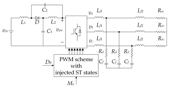
Figure 1.
Standalone configuration of the qZSI.
The analyzed qZSI enables boosting of the input dc voltage (vin) through the utilization of the impedance network and the implementation of ST states. These states involve short-circuiting one or all the inverter phase legs, which is strictly prohibited in conventional VSIs. The equivalent circuits of the qZSI in the non-ST state and ST state are shown in Figure 2a and Figure 2b, respectively. In the non-ST state, the impedance network is coupled to the load allowing power to flow from the dc source to the load (except during the zero switching states). This state results in a forward biased diode D (Figure 2a), charging of the capacitors C1 and C2, and a decrease in the currents through the inductors L1 and L2. During the ST state (typically occurring during the zero switching state), the inverter bridge is short-circuited, which causes reverse biasing of the diode D (Figure 2b), discharging of the capacitors C1 and C2, and an increase in iL1 and iL2.
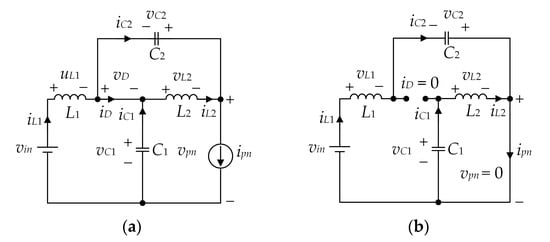
Figure 2.
Equivalent circuits of the qZSI: non-ST state (a) and ST state (b).
The input voltage boost (B) and the mean values of the voltages across the capacitors C1 and C2, denoted as VC1 and VC2, respectively, are determined as follows:
PWM schemes recently proposed for the qZSI are based on the conventional SPWM or SVPWM schemes but adapted to enable injection of the ST states. However, most are based on the conventional SVPWM scheme due to the lower total harmonic distortion (THD) and times higher achievable output ac voltage for the same Ma value compared to the conventional SPWM scheme. In fact, similar can be achieved by injecting a third-harmonic component (1/6 amplitude) into the fundamental sinusoidal signals of the conventional SPWM scheme. This is because the conventional SVPWM is equivalent to an SPWM with injected triangular component of the triple fundamental frequency [20].
2.1. Continuous SVPWM Schemes
The most straightforward approach to inject ST states of constant duration involves introducing two additional dc signals—one positive and one negative—commonly referred to as the simple boost method [15]. In Figure 3a, the waveforms of reference and carrier signals are illustrated for the case of simple-boost space-vector modulation (SBSVM). In this figure, the Ma value is set to 0.7, while the frequency modulation index (Mf) is set to 10. The conventional switching pulses are obtained through the comparison of ac reference signals (vmA, vmB, and vmC) with the triangular carrier signal (vtrian). Simultaneously, the ST state pulses are generated by comparing dc reference signals (vP and vN) with vtrian.
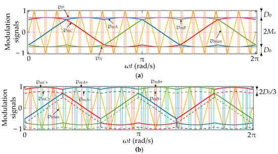
Figure 3.
Waveforms of the SBSVM (a) and the ZSVM6 (b), with Ma = 0.7, Mf = 10 (ST states are denoted by vertical stripes, with different colors denoting different phase legs).
The ST state is activated whenever vtrian is higher than vP or lower than vN. The switching pulses for the transistors are obtained as the output of the logic OR operation between the ST state pulses and the standard switching pulses. This results in the short circuiting of all the inverter phase legs during the ST state, which occurs twice per switching period.
However, the implementation of the SBSVM scheme is more complicated than the standard VSI SVPWM scheme because it requires two additional reference signals (vP and vN) to generate the gate signals.
Another method of injecting ST states involves controlling the upper and lower transistors in the same inverter phase leg using two vertically displaced ac reference signals. The SVPWM scheme depicted in Figure 3b was proposed in [12] and named ZSVM6 in [11]. It is the most widely used SVPWM scheme employing the reference signal displacement and it is notable for having the least amount of inductor current ripple. A small vertical displacement is introduced between the reference signals for the upper and lower transistors, as shown in Figure 3b. It is important to note that this displacement may be adjusted within feasible limits, which allows for decoupled control of Ma and D0. The upper transistors are turned on when the corresponding reference signals (vmA+, vmB+, and vmC+) are larger than the triangular carrier signal (vtrian), whereas the lower transistors are turned on when the corresponding reference signals (vmA−, vmB−, and vmC−) are smaller than the carrier signal. Consequently, due to the displacement, an overlap is generated between each pair of switches in each phase leg. This results in the ST state every time the normal switching transition is bound to occur, which is analogous to implementing negative dead time. The ST state occurs in one phase leg at a time, whereas in each phase leg it occurs twice per switching period. Therefore, there are six ST states in total per switching period, each lasting one-sixth the total ST time. However, they are not evenly distributed within a switching period due to the variable duration of individual active switching states (Figure 3b). This leads to a variable D0 value and induces a low-frequency (LF) ripple in both the currents of the inductors and the voltages across the capacitors in the impedance network. Due to the same reason, the effective switching frequency within the impedance network is, in the worst case, reduced to only twice the bridge switching frequency (2fsw). This reduction contributes to an increase in the high-frequency (HF) ripple.
The fact that the ZSVM6 scheme requires six reference signals for three-phase qZSIs makes its implementation more complicated compared to the standard VSI SVPWM scheme, which requires half as many reference signals.
2.2. Discontinuous SVPWM Schemes
The previously discussed, SBSVM and ZSVM6 schemes fall into the group of continuous PWM schemes, in which all the phase legs are continuously pulse-width modulated. This is not the case with discontinuous PWM schemes because they involve clamping of a phase leg to the positive or negative dc rail for one-third of each fundamental period, while the remaining two phase legs remain pulse-width modulated [13,14]. As a result, the number of switch commutations is reduced compared to the continuous PWM schemes.
The discontinuous SVPWM scheme proposed in [14] for the three-phase qZSI is illustrated in Figure 4a. It is known as the simple-boost discontinuous space-vector (SBDSV) modulation and requires an additional negative dc reference signal (vN). The ST states are injected in all three phase legs simultaneously when the carrier signal (vtrian) is above the largest ac reference signal (max (vmA, vmB, vmC)) or below the dc reference signal. If these conditions are not met, the qZSI is modulated as the conventional VSI. The simultaneous injection of the ST states in all three phase legs results in lower current stress of the bridge transistors compared to ZSVM6. However, since the ST state occurs twice per switching period (as with the SBSVM scheme), the HF ripple in the inductor currents is higher compared to ZSVM6. Still, the need for an additional dc reference signal complicates the implementation of the SBDSV scheme.
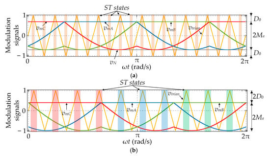
Figure 4.
Waveforms of the SBDSV (a) and the SBMSV (b), with Ma = 0.7, Mf = 10 (ST states are denoted by vertical stripes, with different colors denoting different phase legs).
The corresponding reference signals are given as follows:
where denotes obtained from (2).
Figure 4b shows the waveforms of the discontinuous SVPWM scheme proposed in [13]. It is known as the simple-boost modified space-vector (SBMSV) modulation. In this case, the three-phase qZSI is modulated by comparing the reference signals (vmA, vmB, and vmC) with the carrier signal (vtrian), as is the case in standard PWM schemes. In other words, there is no requirement for any additional ac or dc reference signals. Furthermore, each of the upper transistors is turned on when the corresponding reference signal is larger than or equal to the carrier signal or the other two reference signals, whereas the lower transistors are turned on when the corresponding reference signal is smaller than the carrier signal. This inevitably leads to overlapping between the two transistors in the same phase leg. The ST state occurs in one phase leg at a time, as is the case with ZSVM6. This means that the transistors must withstand higher peak currents compared to SBSVM or SBDSV, where the ST-induced current is evenly distributed in all three phase legs. Lastly, the ST state occurs only once per switching period, which increases the HF ripple in the inductor currents compared to the other previously discussed schemes and particularly ZSVM6.
The corresponding reference signals are given as follows:
where again denotes obtained from (2).
It is important to note that in all the SVPWM schemes discussed in this section, except for the ZSVM6 scheme, the ST duty cycle does not vary over time. By this, the LF ripple in the inductor currents and the capacitor voltages is effectively eliminated. In addition, in these schemes, dead time is not implemented to prevent short-circuiting in the inverter phase legs that may occur outside of the intended ST intervals and lead to higher voltage boost and stress than expected [19]. Moreover, in the case of the SBSVM and SBDSV schemes, the beginning of the ST state is not always synchronized with the beginning of the zero switching state, which may lead to additional switching transitions and, hence, higher switching losses [19]. Finally, again except for ZSVM6, the decoupled control of D0 and Ma has not been implemented for the PWM schemes discussed in this section, although such a possibility was mentioned in [14] for the SBDSV scheme and in [13] for the SBMSV scheme.
3. Proposed Decupled Zero-Sync SVPWM Schemes with Dead Time
This section introduces two novel discontinuous SVPWM schemes for the three-phase qZSI. Both involve dead time injection, as proposed in [19], to prevent uncontrollable increase in the voltage boost and stress due to unintended ST states. The ST states are injected according to the zero-sync method, also proposed in [19], so as to reduce the switching losses. Another significant feature of the two proposed SVPWM schemes is decoupled control of D0 and Ma, provided that D0 < D0max (D0max = 1 − Ma), which opens the possibility of application in closed-loop control systems. The first proposed scheme, named DSV2ST, utilizes two ST states per switching period and is based on the SBDSV scheme from [14], whereas the second proposed scheme, named DSV1ST, utilizes a single ST state per switching period and is based on the SBMSV scheme from [13].
3.1. Decoupled SVPWM with Two ST States per Switching Period (DSV2ST)
Starting from the SBDSV scheme described in Section 2.2, the decoupling of D0 and Ma from Figure 4a can be achieved by shifting the ac reference signals (vmA, vmB, and vmC) upwards and the dc reference signal (vN) downwards by the same amount, as illustrated in Figure 5a. The resulting reference signals are given as
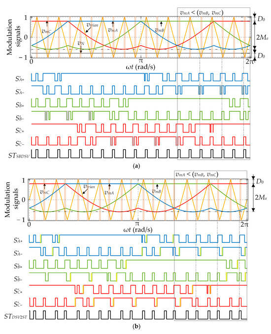
Figure 5.
Waveforms of the decoupled SBDSV (a) and the proposed DSV2ST (b), with Ma = 0.7, Mf = 10, D0 = 0.2 (ST states are denoted by vertical stripes).
Note the similarity between (5) and (3), where the only difference is in the vN value, which, in turn, affects the vertical shift of the ac reference signals. In this case, vN is defined by D0 and not by Ma, with the latter parameter contained in . This shows that D0 and Ma may be independently set within feasible limits. Therefore, the PWM scheme presented in Figure 5a may be referred to as the decoupled SBDSV scheme. Still, apart from the decoupled control, the scheme in Figure 5a shares the same demerits of the SBDSV scheme, discussed in Section 2.2.
In the proposed DSV2ST scheme with dead time, illustrated in Figure 5b, a dc reference signal is removed, whereas a timer is utilized instead to ensure adjustable but constant ST state duration, as shown in Figure 6. The ST state occurs twice per switching period in all three phase legs when the carrier signal is higher than the upper envelope of the ac reference signals or lower than the dc reference signal. Moreover, the ST states are synchronized with the zero switching states, thanks to which all the switching transitions marked with gray color in the lower part of Figure 5a are effectively eliminated. It can be seen that only the lower transistors in the bridge are affected by the proposed synchronization, so the number of eliminated switching transitions is in this case equal to 2Mf, which is twice lower than the number achieved in [19]. Dead-time intervals are marked with yellow color in the lower part of Figure 5b. The corresponding reference signals are given as follows:
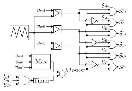
Figure 6.
PWM pulses generation for the proposed DSV2ST scheme.
In (5) and (6), denotes obtained from (2).
3.2. Decoupled SVPWM with a Single ST State per Switching Period (DSV1ST)
Starting from the SBMSV scheme described in Section 2.2 (Figure 4b), the respective reference signals can be shifted vertically so that the minimum of the lower envelope is not necessarily aligned with −1. Such modification is illustrated in Figure 7a, whereas the corresponding reference signals are defined as
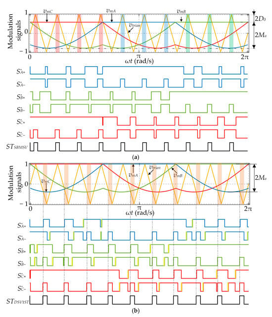
Figure 7.
Waveforms of the decoupled SBMSV (a) and the proposed DSV1ST (b), with Ma = 0.7, Mf = 10, D0 = 0.2 (ST states are denoted by vertical stripes, with different colors denoting different phase legs).
This PWM scheme may be referred to as the decoupled SBMSV scheme. However, it suffers from the same other issues discussed in Section 2.2 for the SBMSV scheme.
Given the above, a novel DSV1ST scheme with dead time is proposed in which the upper envelope of the reference signals is aligned with 1, as illustrated in Figure 7b. The ST state occurs once per switching period when the carrier signal is below the lower envelope of the reference signals, but, as opposed to SBMSV, it occurs in all three phase legs. This results in lower current stress of the bridge transistors. On the downside, the number of switching transitions of the lower transistors in the bridge is higher compared to SBMSV. Again, a timer is utilized to ensure constant and adjustable ST state duration, as shown in Figure 8, while the ST states are synchronized with the zero switching states. Dead-time intervals are marked with yellow color in the lower part of Figure 7b. The corresponding reference signals are defined as
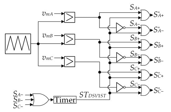
Figure 8.
PWM pulses generation for the proposed DSV1ST scheme.
Once again, in (7) and (8) corresponds to obtained from (2). Also note that (8) does not contain D0 because its value is not defined by the reference signals, but is instead controlled by utilizing the timer.
3.3. Proposed vs. Existing PWM Schemes—A Comparative Study
The equations describing the HF ripple in the inductor currents and the capacitor voltages within the impedance network can be derived based on the voltage-current conditions in the equivalent circuits in Figure 2 and are given as follows:
where TST represents the total duration of ST states per switching period and nST denotes the number of ST states per switching period (see Table 1).

Table 1.
Comparison of the PWM schemes’ features.
In the PWM schemes where the ST states are injected based on the comparison of the triangular carrier signal and the reference signals with constant upper and lower envelopes (SBDSV and SBMSV), the LF ripple does not exist due to the constant D0 value. However, in PWM schemes like ZSVM6, DSV1ST, and DSV2ST, the LF ripple component is present despite the constant duration of the ST state. This is due to the varying D0 value caused by uneven duration of the non-ST states (e.g., unequal spacing between the ST states in Figure 3b). Nevertheless, it is worth noting that the LF ripple is relatively small for the considered PWM schemes, whereas its mathematical derivation is beyond the scope of this study.
Table 1 compares some of the key features of the SVPWM schemes under consideration so as to clarify and highlight the advantages of the proposed schemes. The proposed schemes enable decoupled control of Ma and D0 while also eliminating additional zero switching states and unintended ST states. Among the other schemes listed in Table 1, only ZSVM6 meets all these criteria, but it does so at the expense of needing twice as many reference signals and experiencing notably higher peak currents in the bridge switches, resulting in higher semiconductor losses. As for the current stress imposed by the proposed methods, it is among the lowest recorded, as demonstrated by the experimental waveforms presented later in Section 5.
4. Experimental Setup
4.1. Laboratory Setup of the Quasi-Z-Source Inverter
The experimental setup of the standalone qZSI system from Figure 1, utilized for the evaluation of the proposed PWM schemes, is shown in Figure 9a. The meaning of the numerical markings shown in Figure 9a is as follows:
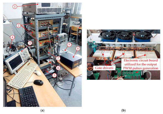
Figure 9.
Laboratory setup of the considered qZSI system (a) and the qZSI bridge with the corresponding gate drivers and electronic circuit board (b).
- Dc power supply 62050H 600S (Chroma, Foothill Ranch, CA, USA); maximum power of 5000 W with voltages up to 600 V and currents up to 8.5 A.
- Hall effect transducers LA 55-P/SP52 (for the inductor current) (LEM International SA, Plan-les-Ouates, Switzerland), CV 3–500 (for the qZSI input voltage) (LEM International SA, Meyrin, Switzerland), and DVL 500 (for the voltages across C1 and C2) (LEM International SA, Meyrin, Switzerland).
- Oscilloscope MDO 3014 (Tektronix, Beaverton, OR, USA).
- MicroLabBox controller board (dSpace, Paderborn, Germany) for the qZSI control.
- qZSI impedance network inductors, built with powder cores T520-26 (Micrometals, Anaheim, CA, USA), with L1 = L2 = 20 mH (unsaturated), RL = 0.5 Ω (at 25 °C), and polypropylene capacitors MKSPI35-50U/1000 (Miflex, Kutno, Poland) with C1 = C2 = 50 µF and ESR = 7.8 mΩ.
- qZSI three-phase inverter bridge (IXBX75N170 IGBTs (Littelfuse, Chicago, IL, USA) with SKHI 22B(R) (Semikron-Danfoss, Nuremberg, Germany) gate drivers) and the custom-developed electronic circuit board for the PWM pulses generation (Figure 9b).
- Self-made LCL filter at the qZSI output stage (Lf1 = 8.64 mH, Lf2 = 4.32 mH, Rf1 = 0.1036 Ω, Rf2 = 0.0518 Ω, Cf = 4 µF, Rd = 10 Ω).
- Power analyzer Norma 4000 (Fluke, Everett, WA, USA) utilized for the measurement of the load power.
- Adjustable three-phase resistive load.
4.2. Hardware Circuitry for Gate Pulses Generation
In this study, an electronic circuit board was specially designed and built to facilitate the implementation of a range of existing PWM schemes for the qZSI, as well as the two proposed schemes. The logic diagram for generating the PWM pulses is depicted in Figure 10. Six PWM channels of the EMC Multi Channel PWM block are utilized to generate the input PWM pulses, namely SA+, SA−, SB+, SB−, SC+, and SC−. This allows for individual control of each transistor in the inverter bridge, enabling the implementation of any PWM scheme that utilizes two vertically displaced ac reference signals in the same inverter leg. The remaining two PWM channels are used to generate the SP and SN pulses, which correspond to the ST signals in the case of PWM schemes that utilize the dc reference signals for ST injection (e.g., SBSVM). It is important to note that the input variables for the EMC Multi Channel PWM block in Figure 10 are the duty cycles dA, dB, and dC, calculated in the MATLAB-Simulink (version 8.6 (R2015b)) environment, which can be obtained from the corresponding ac reference signals vmA, vmB, and vmC as
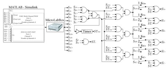
Figure 10.
Logic diagram of the PWM pulses generation.
Digital outputs of the MicroLabBox controller board (i.e., DIO CL1 BIT OUT block in Figure 10) are utilized to generate six additional digital signals, namely SdA+, SdA−, SdB+, SdB−, SdC+, and SdC−. These signals are, for example, required for the implementation of the decoupled variants of the SBMSV and SBDSV schemes.
The logic diagram includes NOR gates in the upper left part to detect the occurrence of zero switching states. The timer is initiated by the logic signal 1 at the beginning of these states. From that moment, the timer holds the logic signal 1 at its output for a precisely set time, so it can be used to control the duration of ST states. This facilitates the injection of zero-synced ST states of adjustable duration, represented by the output signal STtim. As required by some PWM schemes, this signal can be additionally combined with the digital signals SdA+, SdA−, SdB+, SdB−, SdC+, and SdC−. If the timer is used for the ST injection, the switches STA+, STA−, STB+, STB−, STC+, and STC− are set to position 1, whereas they are set to position 2 if the ST states are injected by other means. In the output stage, OR gates are used to generate the output PWM pulses S*A+, S*A−, S*B+, S*B−, S*C+, and S*C−.
Figure 11 shows a photo of the developed electronic circuit board for PWM pulses generation. Apart from the utilized integrated circuits, connectors, and switches, the photo shows the resistor Rt and the capacitor Ct. These two components determine the time constant Tt = Rt ∙ Ct, by which the desired achievable range of D0 can be easily implemented. The reader is referred to [19] for more details.
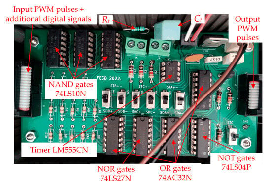
Figure 11.
Photo of the electronic circuit board utilized for PWM pulses generation.
Six PWM schemes were considered for the experimental analysis in this study. These are as follows:
- ZSPWM—continuous zero-sync SPWM scheme with injected third harmonic and dead time, proposed in [19]; it has two ST states per switching period, each occurring in all three phase legs simultaneously (similar to the SBSVM scheme from Figure 3a, but with implemented zero-sync and dead time).
- ZSVM6—continuous decoupled SVPWM scheme reported in [12], and illustrated in Figure 3b; it incorporates six ST states per switching period, each occurring in one phase leg at a time.
- dec. SBDSV—decoupled variant of the discontinuous SVPWM scheme from [14], presented in Figure 5a, with two ST states per switching period, each occurring in all three phase legs simultaneously.
- dec. SBMSV—decoupled variant of the discontinuous SVPWM scheme from [13], illustrated in Figure 5b, with a single ST state per switching period, occurring in a single phase leg.
- DSV2ST—proposed decoupled and discontinuous zero-sync SVPWM scheme with dead time and two ST states per switching period, each occurring in all three phase legs simultaneously (Figure 5b).
- DSV1ST—proposed decoupled and discontinuous zero-sync SVPWM scheme with dead time and a single ST state per switching period, occurring in all three phase legs simultaneously (Figure 7b).
Table 2 provides the corresponding switches position, additional digital signal values, and the values of the SP and SN signals. Note that dtrian in Table 2 is obtained from vtrian, as per (11). Three out of the six considered PWM schemes include dead time implementation, namely, ZSPWM, DSV2ST, and DSV1ST. The corresponding value was in this study set to 0.7 µs to prevent unintended short-circuiting while avoiding previously mentioned negative effects of excessive dead time. The same three PWM schemes utilize the timer for injecting the zero-synced ST states. It is important to note that the developed electronic circuit board, shown in Figure 11, facilitates the implementation of various other PWM schemes that were not considered in this study.

Table 2.
Switches positions and additional digital signal values for considered PWM schemes.
5. Experimental Results and Discussion
The experimental results presented in this section are obtained for three distinct switching frequencies, namely 5 kHz, 10 kHz, and 15 kHz, and three distinct load powers, namely 1000 W, 2000 W, and 3000 W. For all the considered operating points, the input dc voltage (vin) remained constant at 500 V, and the amplitude modulation index (Ma) was maintained at 0.71. At the same time, the duty cycle (D0) was varied in the range 0.1–0.25, which was enabled by the decoupled control feature. To prevent excessive power losses and to avoid overheating the semiconductor switches, D0 was limited to 0.25, which is 0.04 less than the theoretical maximum value.
5.1. System Efficiency and Inverter Voltage Stress
Figure 12 illustrates the system efficiency, which is calculated as the ratio between the load power and the dc source power, thereby encompassing the filter losses as well. However, it is important to note that the filter losses are generally stable for specific load power and fsw settings, regardless of the PWM scheme used. Consequently, the variations in the characteristics shown in Figure 12 accurately reflect the differences in inverter efficiency for the various PWM schemes under consideration. It is evident for all six PWM schemes that the corresponding efficiency reduces with increasing duty cycle. This reduction in efficiency is attributed to the greater voltage stress (as shown in Figure 13), leading to increased switching losses.
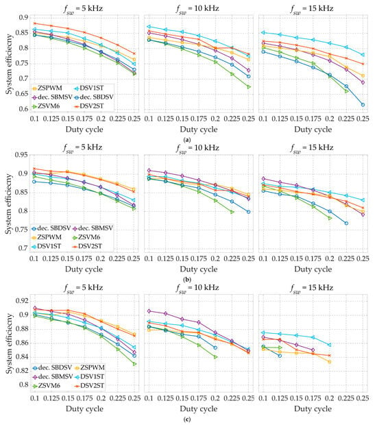
Figure 12.
System efficiency as a function of the duty cycle for the different switching frequencies and inverter power of 1000 W (a), 2000 W (b), and 3000 W (c).
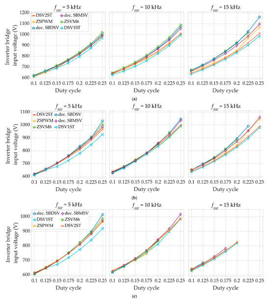
Figure 13.
Inverter bridge input voltage as a function of the duty cycle for the different switching frequencies and inverter power of 1000 W (a), 2000 W (b), and 3000 W (c).
The ZSVM6 scheme exhibits the lowest efficiency, which is due to the six ST states per switching period (i.e., two ST states per phase leg), each occurring in one phase leg at a time. This results in increased current stress, switching losses, and conduction losses of the involved transistors, especially at higher D0 values (i.e., longer ST states). As the duty cycle and switching frequency increase, the efficiency difference between ZSVM6 and the other five PWM schemes grows. Additionally, the ZSVM6 scheme yields the highest voltage stress overall.
The decoupled SBDSV scheme shows only marginal efficiency improvement, despite having three times less ST states per switching period than ZSVM6. On the other hand, the number of switch commutations per switching period is almost doubled with this PWM scheme compared to ZSVM6. In addition, it is the only considered scheme that does not include zero-sync or dead time (ZSVM6 operates with “negative” dead time and does not depend on zero switching states for ST state injection). Both SBDSV and ZSVM6 suffer the most significant efficiency drop with increasing switching frequency. In fact, at the highest considered switching frequency (fsw = 15 kHz), certain data points at higher D0 values could not even be recorded for these two schemes due to the risk of exceeding the maximum allowable temperature of the IGBT-diode pairs in the bridge.
Having only one ST state per switching period proved to be an advantageous feature of the decoupled SBMSV scheme in the context of switching losses, particularly at higher switching frequencies. Moreover, the ST states are for this scheme inherently synchronized with the zero switching states, leading to comparatively higher efficiency than ZSVM6 and SBDSV. However, unlike the remaining three schemes, the decoupled SBMSV scheme does not incorporate dead time, which explains its lower efficiency in most cases.
The PWM schemes with implemented (positive) dead time, namely ZSPWM, DSV2ST, and DSV1ST, show reduced voltage stress, with DSV1ST particularly excelling in this area. These schemes generally achieve higher efficiency, with DSV1ST performing best at higher switching frequencies, whereas DSV2ST is the most efficient at lower switching frequencies. The latter scheme ensures the lowest voltage stress, whereas the DSV1ST scheme is second best with regard to that criterion. The ZSPWM scheme, while reducing voltage stress compared to the considered existing PWM schemes, still has higher voltage stress than the DSV1ST scheme and similar to that of the DSV2ST scheme. Its efficiency is medium to high at low switching frequencies and load powers, but declines notably with increasing switching frequency, particularly at heavier loads.
5.2. Inductor Current Ripple and Output Current THD
Figure 14 demonstrates that the ZSVM6 scheme excels in terms of inductor current ripple, outperforming other schemes based on this metric. The superior performance of ZSVM6 in this aspect was expected and is attributed to its high number of ST states per switching period, which, on average, results in the highest effective switching frequency of the impedance network. On the other hand, the worst PWM schemes by the same metric are those with only one ST state per switching period, namely the proposed DSV1ST scheme and the decoupled SBMSV scheme. However, it is exactly due to the high number of ST states per switching period, occurring in individual phase legs and leading to relatively high switching and conduction losses, that the ZSVM6 scheme is characterized by the narrowest achievable range of operation. For the remaining three PWM schemes, the inductor current ripple values are close to those recorded for ZSVM6, but they manage to maintain a broader operating range, which is only slightly compromised at the highest considered switching frequency and load power. Overall, as the switching frequency increases, the discrepancies in ripple values among the different PWM schemes become less pronounced.
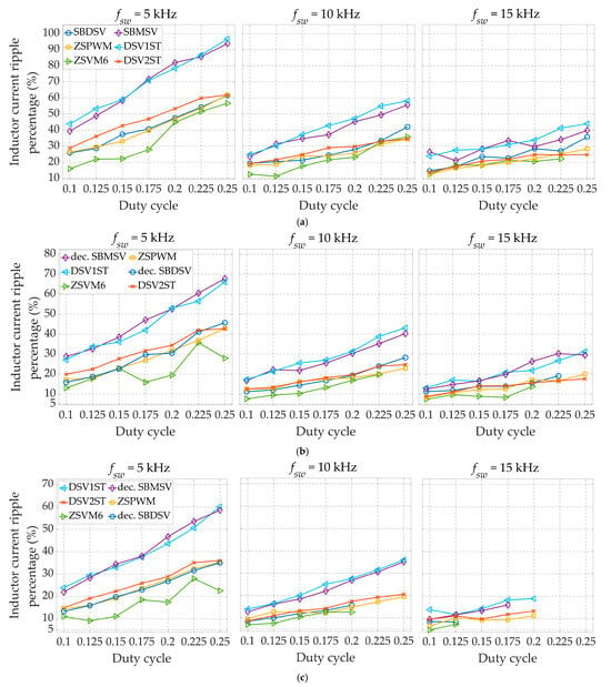
Figure 14.
Inductor current ripple percentage as a function of the duty cycle for the different switching frequencies and inverter power of 1000 W (a), 2000 W (b), and 3000 W (c).
The system under consideration has a nominal power of 3 kW. If, for example, a tolerance for the inductor current ripple at the nominal power is set at 20%, the results in Figure 14 indicate that only the ZSVM6 scheme can achieve this requirement across most of the considered D0 range at fsw = 5 kHz. However, when the switching frequency is increased to 10 kHz, the number of PWM schemes capable of meeting this ripple requirement expands to four, including the proposed DSV2ST scheme. Nonetheless, this increase in switching frequency also limits the highest attainable D0 value to 0.2 for ZSVM6 and SBDSV. It is important to note that for DSV1ST and SBMSV, the inductance in the impedance network would still need to be doubled to reach the target ripple value. Further increasing the switching frequency to 15 kHz allows all considered PWM schemes to achieve the desired inductor current ripple. However, at this frequency, none of them can exceed D0 = 0.2. Specifically, for ZSVM6 and SBDSV, the maximum D0 value is further restricted to 0.125.
Figure 15 shows the recorded THD values of the load phase currents. For all PWM schemes, in most observed cases, there is a trend of increasing THD with the duty cycle. The proposed DSV1ST scheme ranks as the least effective in terms of THD. However, even in the worst case considered (i.e., 5 kHz and 1000 W), the corresponding THD value remained below 4%. Interestingly, the ZSVM6 scheme is the only one exhibiting a noticeable improvement in THD as the D0 increases. Despite ZSVM6 being one of the better schemes in this regard, it is important to remind that this comes at the expense of a reduced D0 range at higher switching frequencies. The ZSPWM and SBMSV schemes also stand out as being among the top three in terms of THD performance, whereas the other proposed scheme, DSV2ST, demonstrated moderate performance with respect to THD.
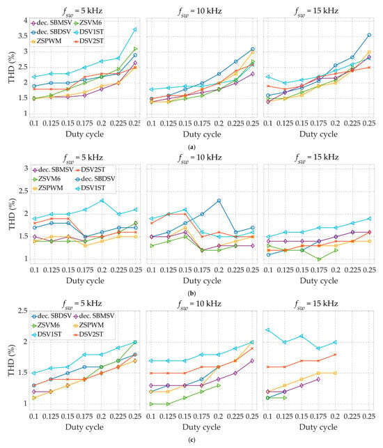
Figure 15.
Output current THD as a function of the duty cycle for the different switching frequencies and inverter power of 1000 W (a), 2000 W (b), and 3000 W (c).
Merits (+) and demerits (−) of the proposed PWM schemes are summarized below. Some of them are common to both methods as follows:
- +
- Higher output voltage for the same Ma value compared to the conventional SPWM scheme.
- +
- Decoupled control of D0 and Ma.
- +
- Reduced number of switch commutations compared to continuous PWM schemes.
- +
- Lower current stress of the bridge transistors compared to PWM schemes where ST is injected in one leg at a time.
- +
- No additional reference signals compared to the conventional SPWM or SVPWM schemes.
- −
- Uneven number of switch commutations of the upper and lower transistors in the bridge.
- −
- Timer required for D0 control.
The following features are specific to the DSV1ST scheme:
- +
- Highest efficiency at higher switching frequencies (otherwise moderate efficiency).
- +
- Lowest voltage stress for all considered combinations of switching frequency and load power.
- −
- Highest inductor current ripple, along with the SBMSV scheme, due to a single ST state per switching period.
- −
- Highest load current THD, particularly at lower switching frequencies and/or heavier loads.
Lastly, the following features are specific to the DSV2ST scheme:
- +
- Highest efficiency at lower switching frequencies (otherwise moderate efficiency).
- +
- Second lowest voltage stress for all considered combinations of switching frequency and load power.
- +
- Similar inductor current ripple as with other PWM schemes having two ST states per switching period (ZSPWM and SBDSV).
- −
- Moderate load current THD, which gets slightly higher at heavier loads in combination with medium to high switching frequencies.
5.3. Voltage and Current Waveforms
In addition to the previously presented steady-state characteristics, experimental waveforms were recorded for the six considered PWM schemes. These waveforms, presented in Figure 16, Figure 17 and Figure 18, include the current through L1 (cyan), the load phase current (green), and the voltages across C1 (magenta) and C2 (yellow). The currents were measured by means of the current clamps TT-CC 770 (Testec, Frankfurt, Germany), whereas the voltages were measured by means of the differential probes TT-SI 9101 (Testec, Frankfurt, Germany). All the waveforms were recorded for the following parameters: fsw = 10 kHz, vin = 500 V, Ma = 0.71, D0 = 0.225, and the load power of 1000 W. Note that the time axes of the first three channels are all aligned and positioned at the bottom of the screen, whereas the time axis of the fourth channel is centered vertically.
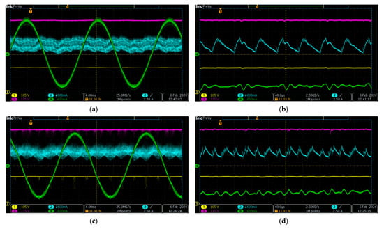
Figure 16.
Experimental waveforms of the considered continuous PWM schemes: ZSPWM (a), zoomed ZSPWM (b), ZSVM6 (c), and zoomed ZSVM6 (d).
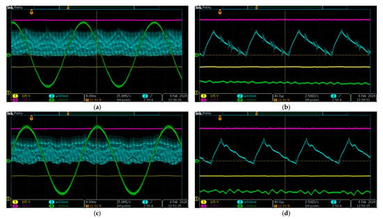
Figure 17.
Experimental waveforms of the considered discontinuous PWM schemes with one ST state per switching period: dec. SBMSV (a), zoomed dec. SBMSV (b), DSV1ST (c), and zoomed DSV1ST (d).
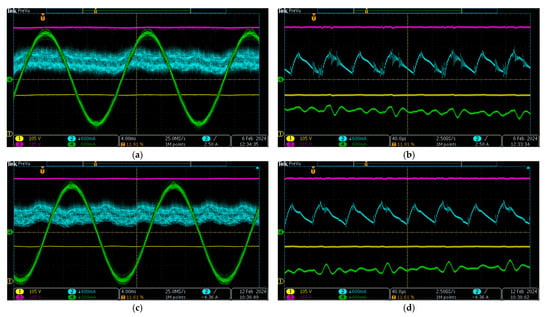
Figure 18.
Experimental waveforms of the considered discontinuous PWM schemes with two ST states per switching period: dec. SBDSV (a), zoomed dec. SBDSV (b), DSV2ST (c), and zoomed DSV2ST (d).
The decrease of the inductor current ripple with the increase of the number of ST states per switching period is clearly visible. Consequently, the smallest ripple is observed for the ZSVM6 scheme (Figure 16c,d), whereas the largest ripple is observed for the two PWM schemes in Figure 17. At the same time, the ZSVM6 scheme, having the highest number of ST states per period, induces the highest electromagnetic interference (EMI) in the recorded waveforms, whereas on the other side of the spectrum is the DSV1ST scheme with the lowest number of switch commutations and, hence, the lowest induced EMI noise (Figure 17c,d). Both the proposed PWM schemes induce lower levels of EMI noise in comparison with the discontinuous PWM schemes that have the same number of ST states per switching period, which is evident from the lack of HF oscillations in the corresponding zoomed waveforms of the inductor current in Figure 17b,d and Figure 18b,d, respectively.
5.4. Current Stress
Based on prior theoretical analysis, different considered PWM schemes induce varying levels of current stress on the bridge switches. Firstly, it is observed that the current stress of the upper and lower switches is balanced only in the case of continuous PWM schemes, namely, ZSPWM and ZSVM6. Furthermore, the peak current experienced by the bridge switches tends to be higher in PWM schemes where ST states are injected sequentially, (i.e., phase by phase), namely, ZSVM6 and SBMSV (Table 1). Figure 19 shows the experimentally obtained instantaneous values of the current through L1 (cyan), the phase current at the bridge output (green), and the current through the upper transistor of the same phase (magenta), which was measured by means of the Rogowski coil probe CWT UM/015/B/1/80 (PEM, San Carlos, CA, USA). The upper transistor is here chosen because the respective maximum current is higher or equal to that of the lower transistor in the same phase leg for all the considered PWM schemes. The depicted time frame spans two switching periods and coincides with the phase current reaching a positive peak. The ST states are distinguished since the inductor current reaches its maximum value at the end of these states. The phase current and the inductor current combined define the maximum current through the upper transistor, as per Table 1, whereas the recorded waveforms confirm that the largest corresponding value is inherent to ZSVM6 and SBMSV schemes (Figure 19b and Figure 19d, respectively). Note that for the ZSPWM scheme (Figure 19a), which is not included in Table 1, the maximum switch current is the same as for other schemes in which ST states are simultaneously injected in all three phase legs.
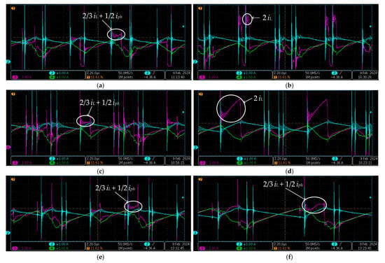
Figure 19.
Current stress of the considered PWM schemes: ZSPWM (a), ZSVM6 (b), dec. SBDSV (c), dec. SBMSV (d), DSV2ST (e), and DSV1ST (f).
5.5. Thermal Stress
Thermal stress is known to affect the reliability of semiconductor switches and power converter efficiency. To assess the thermal stress induced by the considered PWM schemes, the case temperature of the upper and lower IGBT-diode pair from the same phase leg was recorded by means of the thermal camera Testo 865 (Testo SE Titisee-Neustandt, Germany). Figure 20 shows the results obtained for the same operating parameters as those presented in Figure 16, Figure 17 and Figure 18, where “H” represents the hotspot.
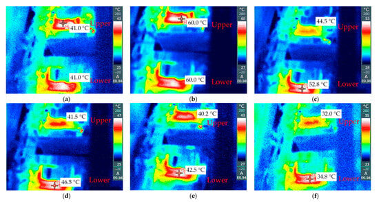
Figure 20.
Thermal stress of the considered PWM schemes: ZSPWM (a), ZSVM6 (b), dec. SBDSV (c), dec. SBMSV (d), DSV2ST (e), and DSV1ST (f).
Only the continuous ZSPWM and ZSVM6 schemes result in symmetric thermal stress of the upper and lower switches, whereas the ZSVM6 scheme yields the highest overall temperature. The remaining discontinuous PWM schemes lead to higher thermal stress of the lower IGBT-diode pair due to the uneven number of switch commutations of the upper and lower switches. The lowest thermal stress was observed for the proposed DSV1ST scheme, with almost twice lower temperatures compared to the ZSVM6 scheme.
6. Conclusions
This paper has successfully addressed the development and implementation of advanced PWM schemes for three-phase qZSIs, highlighting their significant potential in enhancing the efficiency and reliability of low-voltage-fed applications. Two innovative SVPWM schemes were introduced that overcame the limitations of existing PWM schemes by providing independent control of the amplitude modulation index and duty cycle, crucial for optimizing performance in closed-loop applications. The experimental testing showed that the proposed decoupled SVPWM schemes not only ensure improved synchronization of the zero switching states and the ST states and prevent unintentional short-circuiting outside of the ST states, but also demonstrates up to 6.8% higher efficiency and up to 7.5% reduced voltage stress. The enhanced efficiency and reduced voltage stress contribute directly to lower operational costs and improved sustainability of systems employing qZSIs. This is particularly valuable in applications where maximizing energy conversion efficiency is of great importance, such as renewable energy systems (e.g., PV panels and wind turbines), electric vehicles (longer ranges and shorter charging times), and uninterruptible power supplies. Moreover, reduced EMI noise means that qZSI systems employing the proposed SVPWM schemes can meet stricter regulatory standards and exhibit less interference with nearby electronic devices, whereas lower thermal stress extends the lifespan of semiconductor components, thereby enhancing system reliability and reducing maintenance costs. The findings of this research underscore the importance of continuous innovation in PWM techniques to meet the evolving demands of power electronics systems. They have the potential to significantly improve the performance and controllability of qZSIs, thereby promoting the widespread adoption of this power converter topology in various applications and facilitating the development of more efficient and reliable power conversion systems.
Author Contributions
Conceptualization, I.G., M.B. and D.V.; methodology, I.G., D.V., M.B. and I.M.; software, I.G. and I.M.; validation, I.G., M.B. and D.V.; formal analysis, I.G., M.B. and D.V.; investigation, I.G.; resources, D.V.; data curation, I.G., M.B. and D.V.; writing—original draft preparation, M.B. and I.G.; writing—review and editing, I.G., M.B. and D.V.; visualization, I.G.; supervision, D.V. and I.M.; project administration, D.V. and M.B.; funding acquisition, D.V. and M.B. All authors have read and agreed to the published version of the manuscript.
Funding
This research received no external funding.
Data Availability Statement
The data presented in this study are available on request from the corresponding author.
Conflicts of Interest
The authors declare no conflict of interest.
References
- Anderson, J.; Peng, F.Z. Four quasi-Z-Source inverters. In Proceedings of the 2008 IEEE Power Electronics Specialists Conference, Rhodes, Greece, 15–19 June 2008; pp. 2743–2749. [Google Scholar]
- Monjo, L.; Sainz, L.; Mesas, J.J.; Pedra, J. State-Space Model of Quasi-Z-Source Inverter-PV Systems for Transient Dynamics Studies and Network Stability Assessment. Energies 2021, 14, 4150. [Google Scholar] [CrossRef]
- Liu, Y.; Ge, B.; Abu-Rub, H.; Peng, F.Z. Modelling and controller design of quasi-Z-source inverter with battery-based photovoltaic power system. IET Power Electron. 2014, 7, 1665–1674. [Google Scholar] [CrossRef]
- Liang, W.; Liu, Y.; Shen, Y. Active Power Control Integrated With Reactive Power Compensation of Battery Energy Stored Quasi-Z Source Inverter PV Power System Operating in VSG Mode. IEEE J. Emerg. Sel. Top. Power Electron. 2023, 11, 339–350. [Google Scholar] [CrossRef]
- Do, T.V.; Kandidayeni, M.; Trovão, J.P.F.; Boulon, L. Dual-Source High-Performance Active Switched Quasi-Z-Source Inverter for Fuel Cell Hybrid Vehicles. IEEE Trans. Power Electron. 2023, 38, 12497–12507. [Google Scholar] [CrossRef]
- García-Triviño, P.; Sarrias-Mena, R.; García-Vázquez, C.A.; Llorens-Iborra, F.; Sánchez-Sainz, H.; Fernández-Ramírez, L.M. Hydrogen based configurations for an overhead crane with quasi-Z-source inverter. Sustain. Energy Technol. Assess. 2023, 57, 103297. [Google Scholar] [CrossRef]
- Fang Zheng, P. Z-source inverter. IEEE Trans. Ind. Appl. 2003, 39, 504–510. [Google Scholar] [CrossRef]
- Ellabban, O.; Van Mierlo, J.; Lataire, P. Experimental Study of the Shoot-Through Boost Control Methods for the Z-Source Inverter. EPE J. 2011, 21, 18–29. [Google Scholar] [CrossRef]
- Fang Zheng, P.; Miaosen, S.; Zhaoming, Q. Maximum boost control of the Z-source inverter. IEEE Trans. Power Electron. 2005, 20, 833–838. [Google Scholar]
- Shen, M.; Jin, W.; Joseph, A.; Peng, F.Z.; Tolbert, L.M.; Adams, D.J. Maximum constant boost control of the Z-source inverter. In Proceedings of the Conference Record of the 2004 IEEE Industry Applications Conference, 39th IAS Annual Meeting, Seattle, WA, USA, 3–7 October 2004; pp. 1–147. [Google Scholar]
- Liu, Y.; Ge, B.; Abu-Rub, H.; Peng, F.Z. Overview of Space Vector Modulations for Three-Phase Z-Source/Quasi-Z-Source Inverters. IEEE Trans. Power Electron. 2014, 29, 2098–2108. [Google Scholar] [CrossRef]
- Loh, P.C.; Vilathgamuwa, D.M.; Lai, Y.S.; Chua, G.T.; Li, Y. Pulse-width modulation of Z-source inverters. IEEE Trans. Power Electron. 2005, 20, 1346–1355. [Google Scholar] [CrossRef]
- Abdelhakim, A.; Davari, P.; Blaabjerg, F.; Mattavelli, P. Switching Loss Reduction in the Three-Phase Quasi-Z-Source Inverters Utilizing Modified Space Vector Modulation Strategies. IEEE Trans. Power Electron. 2018, 33, 4045–4060. [Google Scholar] [CrossRef]
- Liu, P.; Xu, J.; Sun, M.; Yuan, J.; Blaabjerg, F. New Discontinuous Space Vector Modulation Strategies for Impedance-Source Inverter With Superior Thermal and Harmonic Performance. IEEE Trans. Ind. Electron. 2022, 69, 13079–13089. [Google Scholar] [CrossRef]
- Siwakoti, Y.P.; Peng, F.Z.; Blaabjerg, F.; Loh, P.C.; Town, G.E.; Yang, S. Impedance-Source Networks for Electric Power Conversion Part II: Review of Control and Modulation Techniques. IEEE Trans. Power Electron. 2015, 30, 1887–1906. [Google Scholar] [CrossRef]
- Ayad, A.; Kennel, R. A comparison of quasi-Z-source inverters and conventional two-stage inverters for PV applications. EPE J. 2017, 27, 43–59. [Google Scholar] [CrossRef]
- Khajesalehi, J.; Sheshyekani, K.; Hamzeh, M.; Afjei, E. High-performance hybrid photovoltaic -battery system based on quasi-Z-source inverter: Application in microgrids. IET Gener. Transm. Distrib. 2015, 9, 895–902. [Google Scholar] [CrossRef]
- Liu, W.; Yang, Y.; Kerekes, T.; Liivik, E.; Blaabjerg, F. Impedance Network Impact on the Controller Design of the QZSI for PV Applications. In Proceedings of the 2020 IEEE 21st Workshop on Control and Modeling for Power Electronics (COMPEL), Aalborg, Denmark, 9–12 November 2020; pp. 1–6. [Google Scholar]
- Grgić, I.; Vukadinović, D.; Bašić, M.; Bubalo, M. Efficiency Boost of a Quasi-Z-Source Inverter: A Novel Shoot-Through Injection Method with Dead-Time. Energies 2021, 14, 4216. [Google Scholar] [CrossRef]
- Vukosavic, S.N. Grid-Side Converters Control and Design, 1st ed.; Springer: Cham, Switzerland, 2018. [Google Scholar]
Disclaimer/Publisher’s Note: The statements, opinions and data contained in all publications are solely those of the individual author(s) and contributor(s) and not of MDPI and/or the editor(s). MDPI and/or the editor(s) disclaim responsibility for any injury to people or property resulting from any ideas, methods, instructions or products referred to in the content. |
© 2024 by the authors. Licensee MDPI, Basel, Switzerland. This article is an open access article distributed under the terms and conditions of the Creative Commons Attribution (CC BY) license (https://creativecommons.org/licenses/by/4.0/).