Article

Design Procedure of Cascaded Multilevel Inverter for High-Power Amplifier in SONAR System

1
Research & Development Division, Tin Technology Co., Ltd., Seongnam 13212, Republic of Korea
2
Agency for Defense Development, Changwon 51678, Republic of Korea
3
Electrical Engineering Department, Konkuk University, Seoul 05029, Republic of Korea
*
Author to whom correspondence should be addressed.
Energies 2024, 17(7), 1581; https://doi.org/10.3390/en17071581
Submission received: 12 December 2023 / Revised: 19 February 2024 / Accepted: 14 March 2024 / Published: 26 March 2024
(This article belongs to the Section F: Electrical Engineering)

Abstract

:
In recent years, there has been a trend toward expanding the operating frequency range and increasing the output power of Sound Navigation and Ranging (SONAR) systems to enhance their acoustic detection capabilities. However, due to this increase in operational power, the electrical capacity of amplifiers for SONAR system operation also increases, necessitating High-Power Amplifiers. When configured with a single amplifier, as in conventional methods, the volume of amplifiers increases due to volumetric increases in heat dissipation, components, and windings. These issues are detrimental to SONAR amplifier installation, mobility, maintenance, and equipment lifespan due to stress on individual components. Additionally, amplifiers for SONAR systems are comprised of power conversion devices, transformers for LC filters and matching, necessitating consideration of LC filters and matching transformers for enhancing voltage quality and efficiency to improve amplifier performance transmitted to SONAR transducers. However, previous research has focused on single-amplifier design methods, neglecting such considerations. Therefore, this paper proposes a design technique that overcomes the drawbacks of using the conventional design method by configuring multiple H-bridge inverters in a cascade format and utilizes one of the optimization algorithms, Particle Swarm Optimization (PSO), to derive amplifier design techniques that optimize component parameters for enhancing high-capacity amplifier performance. Subsequently, theoretical analysis, simulations, and experimental results comparing the proposed high-power amplifier design method with conventional single-amplifier design methods demonstrate similar error rates in operational frequency bands.

1. Introduction

Due to the expansion of industrial sectors and the increased demand for electricity usage in various industrial applications [1,2,3], higher power consumption is required. In recent years, for fields utilizing intermediate voltage and megawatt-scale power, single-power device configuration for power converters has become challenging due to component specifications. Therefore, to address these issues, multi-stage power converter structures or power converters with direct/parallel switch configurations have been introduced. The concept of multi-stage converters was introduced in 1975. The term “multi-stage” refers to a three-level converter. Subsequently, several multi-stage converter topologies have been developed [2]. In terms of multi-stage topologies, there are three main commercial topologies. First, the voltage source inverter: NPC (Neutral Point Clamped); second, the cascaded H-bridge (CHB) and Flying Capacitor (FC) [4,5,6]; and third, modular topologies. Sound Navigation and Ranging (SONAR) refers to acoustic detection by converting the voltage input to SONAR transducers into sound waves. SONAR requires high-quality voltage input to ensure accurate acoustic detection. However, while research on low-capacity amplifiers is active, design procedures for high-capacity amplifiers have not progressed, as the design of high-capacity amplifiers typically relies on using multiple low-capacity amplifiers, and research on design procedures based on the relationship between the overall capacity of amplifiers and the stages of amplifiers using multi-stage configurations has not been conducted. Therefore, in this study, based on the items necessary for driving SONAR sensors in Section 2.2, we theoretically analyze the correlation between high-power amplifiers and multi-stage high-power amplifiers, propose a design method for high-power amplifiers based on this analysis, and validate the suitability of the proposed method through simulations and experiments using reduced capacity.

2. Amplifier Topology for SONAR Systems

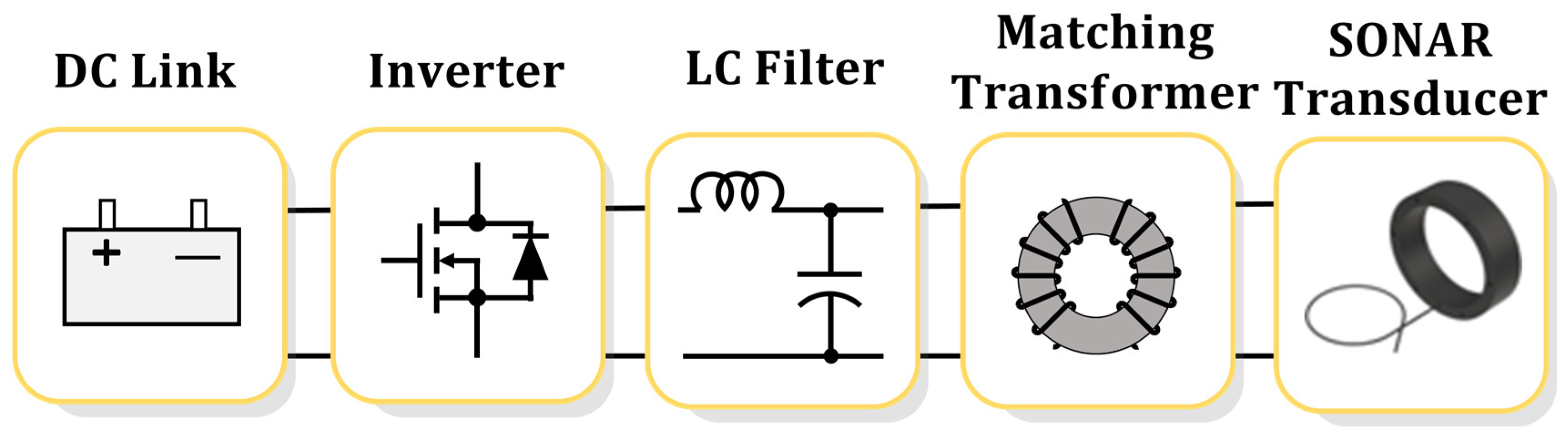
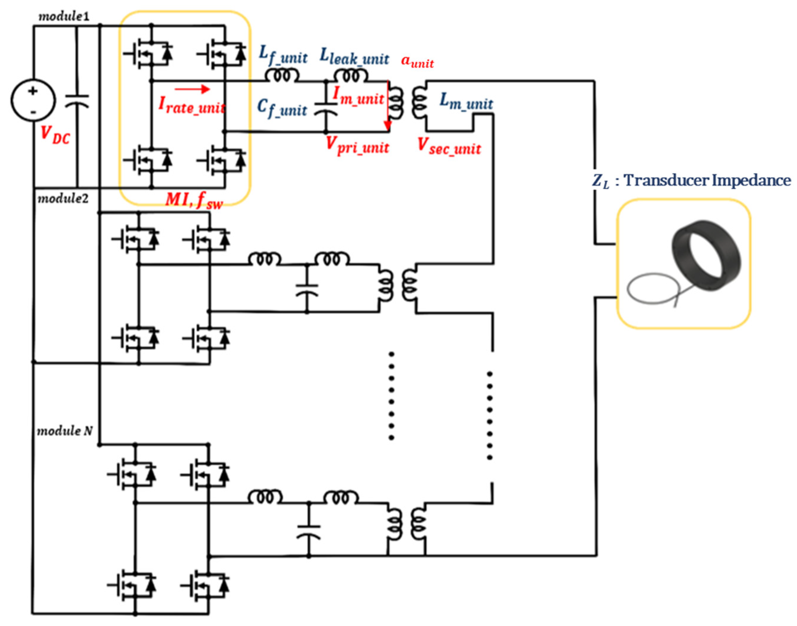
SONAR is used to detect underwater objects by converting electrical energy into sound. The SONAR power system contains the following components, as shown in Figure 1 [7,8,9]. (1) A direct-current (DC) power supply serves as the electrical energy source required for generating acoustic energy. (2) A power converter that converts the DC voltage into alternating current (AC) to provide the desired electrical energy supply for the desired sound signal intensity. (3) An LC filter (or low-pass filter) that removes unnecessary frequencies for acoustic detection. (4) An impedance-matching transformer that eliminates the reactive power generated by the material characteristics of the SONAR sensor. (5) The SONAR sensor converts the input electrical signal into an acoustic signal.

2.1. SONAR Sensor Characteristics

Recently, the development focus of SONAR technology has shifted toward increasing the detection accuracy within the same signal. Research efforts have been directed toward signal analysis techniques, optimal underwater target detection patterns, and the study of signal spectrum variations and interference [11]. Another trend has aimed to enhance detection performance through multiple sensors, high output power, and broadband frequency usage, with the aim of improving detection precision, resolution, and range. To achieve these performance improvements, SONAR sensors are designed and manufactured to achieve a high output, operate at high pressures, and support broadband frequencies. Accordingly, various sensors with distinct characteristics have been developed, as outlined in Table 1 [12]. To satisfy the requirements for acoustic detection performance, the free-flooded ring (FFR) sensor, which is characterized by structural features that make it suitable for deep-sea operation and minimal frequency-specific variations when operating in the broadband mode, was selected in this study [12,13,14].

2.2. High-Power Amplifier Topology
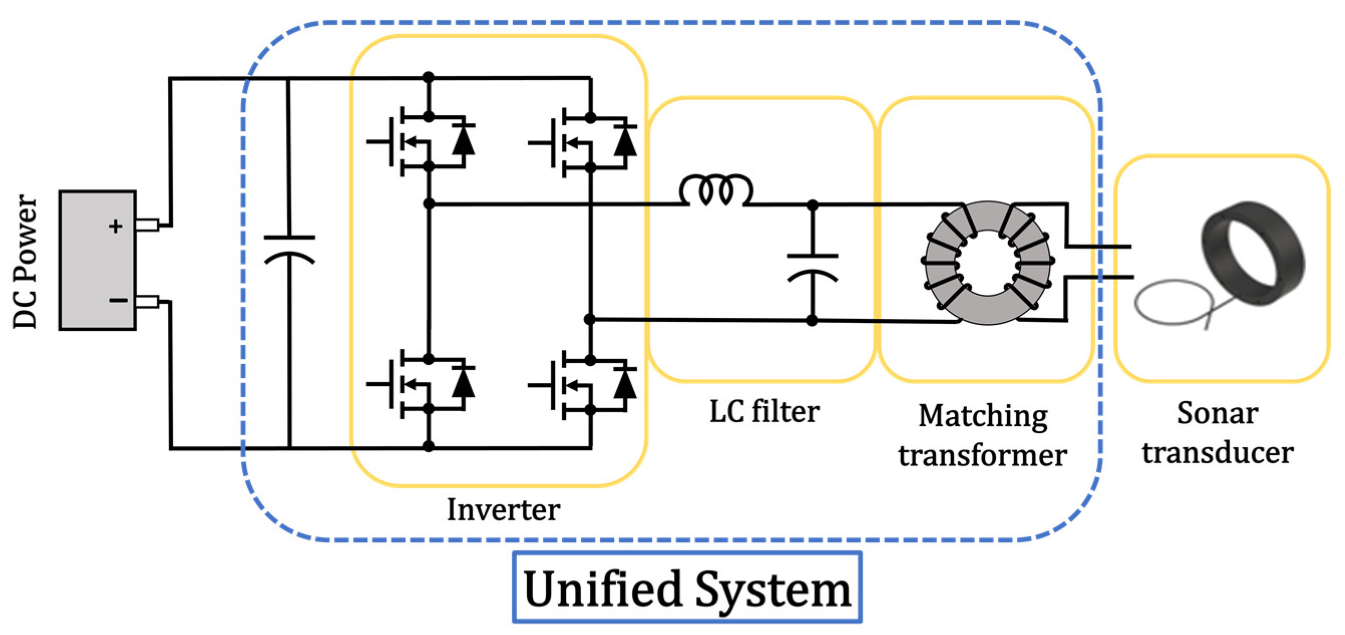
As depicted in Figure 1, traditional SONAR amplifier operation involves the generation of voltage in a sinusoidal waveform for SONAR through high-speed switching of the converter, resulting in sine-wave synthesis and high-frequency removal via the LC filter. Furthermore, to address problems related to the quality of the harmonic content in the voltage applied to the SONAR sensor and volume-related concerns of the converter, a matching frequency within the operating frequency range of the SONAR sensor was selected to design a matching transformer, as discussed by previous researchers [15,16]. Additionally, an efficient power amplification method using the Class E technique has been proposed to address the efficiency problems arising from power converter switching [16].
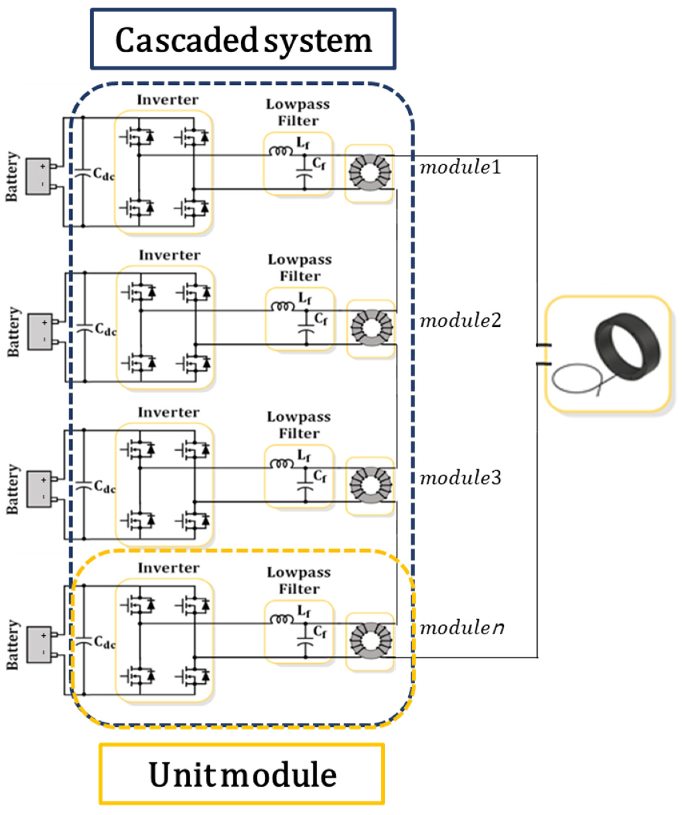
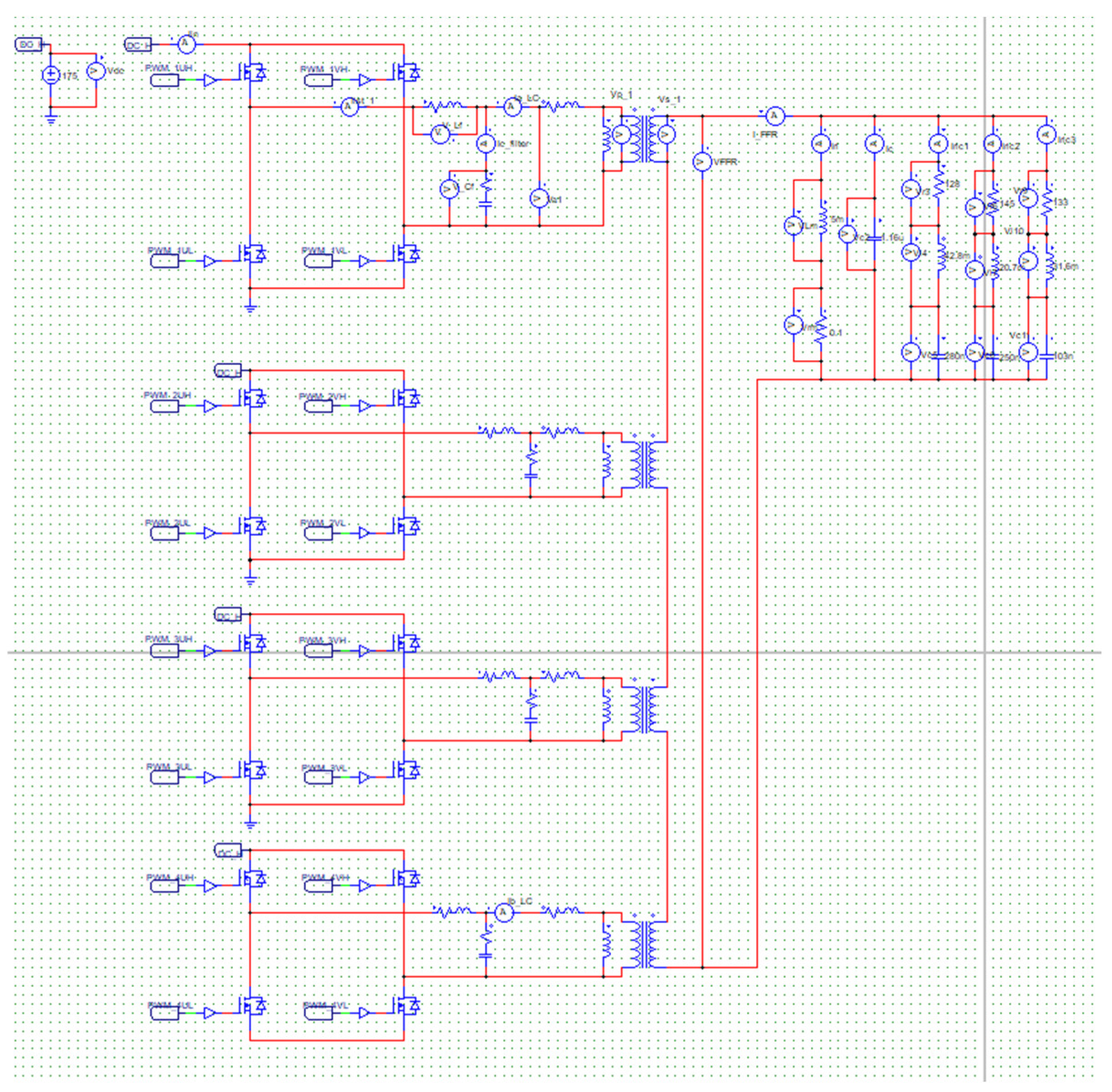
However, as depicted in Figure 2, when utilizing multiple SONAR sensors with a single amplifier, in the event of abnormal operation of the amplifier, it suffices to avoid using the amplifier corresponding to the malfunctioning sensor. On the other hand, when driving a single sensor with a single amplifier, contingency measures for emergency operation owing to amplifier malfunctions must be considered. Furthermore, for the freedom of repair and mobility by personnel, such as operators and maintenance workers, high-capacity amplifiers adopt a topology configuration using multiple legs or a full-bridge serial arrangement in a multilevel approach [1,17,18,19]. However, extensive research on high-capacity amplifier designs has not been conducted.
In single-power converters ranging from several kilowatts to tens of kilowatts, high-frequency switching results in high total harmonic distortion (THD), which adversely affects the quality of the generated acoustic waves [7]. As depicted in Figure 3, to satisfy the demands of increased inverter switching speed and reduced volume and considering the proper functioning of the amplifier under adverse conditions, ease of transport, and replacement, a high-capacity amplifier is configured with a cascaded arrangement in the context of multi-kW SONAR power amplifiers. However, to achieve effects similar to those of the conventional single-amplifier configuration when constructing a cascaded amplifier, the design must address the following aspects:
  • Improvement in harmonic quality owing to the LC filter;
  • Increase in power efficiency owing to the reduction in the amplifier reactive power via the matching transformer;
  • Prevention of energy sharing between serial modules based on phase delays caused by the LC filter and matching transformer in each serial module;
  • Minimal changes in the voltage delivery characteristics of the amplifier output within the operating frequency range of the SONAR sensor.
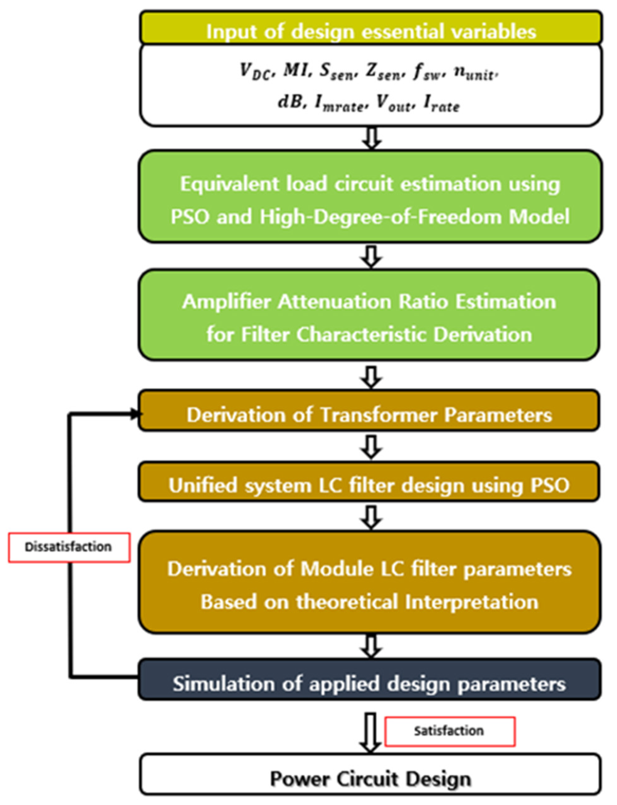
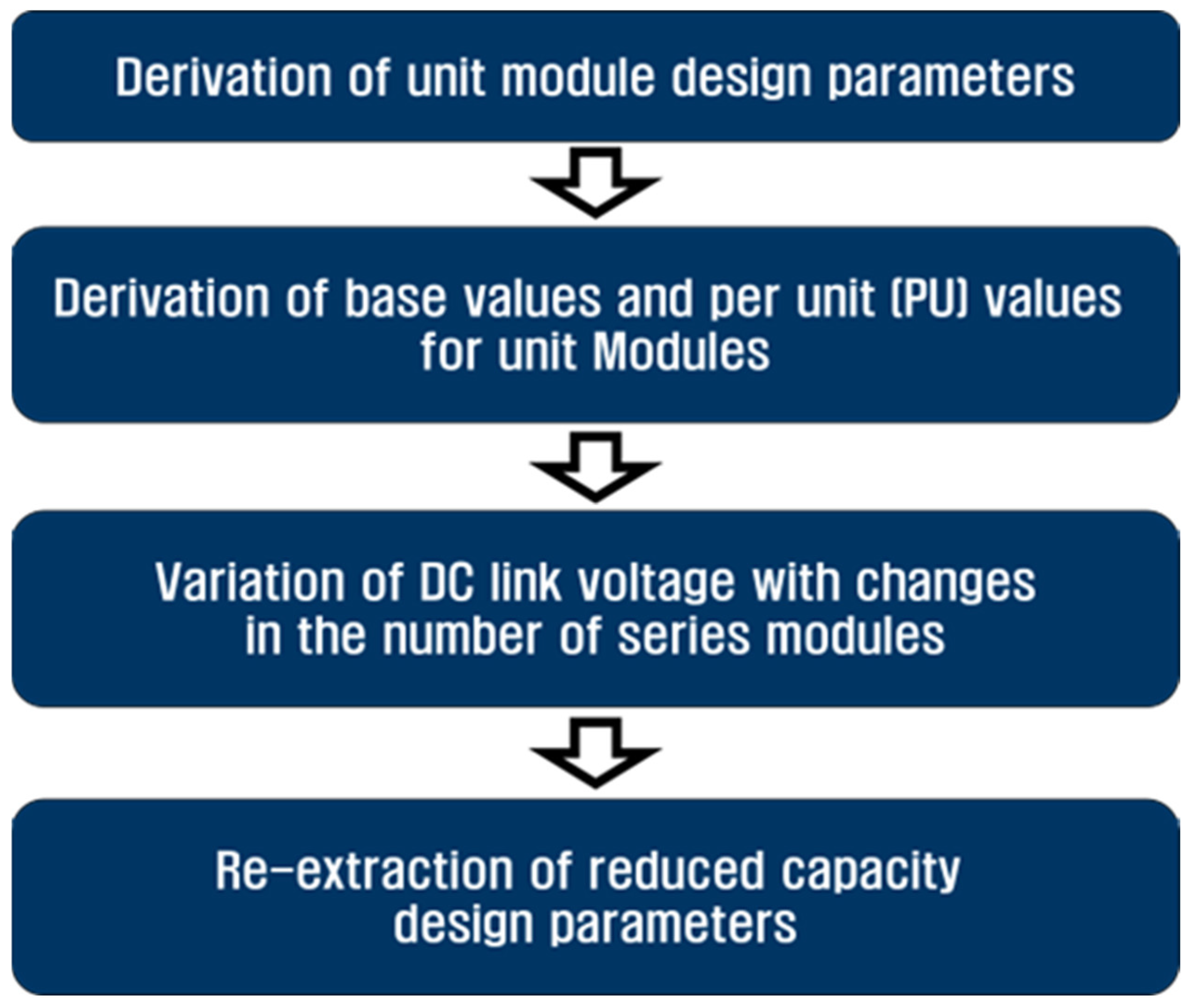
Considering the four key considerations outlined above, this paper proposes a procedure for designing high-power SONAR amplifiers, as depicted in Figure 4. Initially, the necessary design parameter variables for the high-power amplifier are input. Thereafter, based on the load characteristics when the amplifier is used, an equivalent electrical circuit is derived [20]. In the third step, the cutoff frequencies and attenuation ratios are set for the simultaneous design of the LC filter and transformer to derive the design parameters of the single system. Subsequently, the relationships between the design parameters within the modules are derived using equations related to the single and serial system modules. The procedure reveals that the theoretically analyzed amplifier characteristics align closely with the simulation results. Therefore, the mathematical relationships between the component parameters within a single system are first derived to address the considerations for the high-power SONAR amplifier design outlined in this paper, as shown in Figure 2, along with those between the component parameters for constructing a serial system amplifier, as shown in Figure 3. These relationships are then used to facilitate the parameter derivation. Finally, using the relationships between the design parameters of a single system and serial module parameters, a design method for high-power amplifiers with a serial topology, such as that depicted in Figure 3, is developed. The developed method is validated through theoretical analysis, simulations, and experimentation using a reduced-capacity topology to assess its suitability.

2.3. Relationship between Unified Amplifier System and Cascaded Amplifier System for Sonar Applications

To derive the mutual relationships between the design parameters within the structures of Figure 2 and Figure 3, we first employ Thevenin’s equivalent circuit to formulate expressions for the supply voltage and load of the reference single system. Subsequently, we similarly utilize Thevenin’s equivalent circuit to derive the mutual relationships within the serial system. We then compare these equations with a reference equation to deduce the relationship between the number of serial modules (n) and the design parameters.
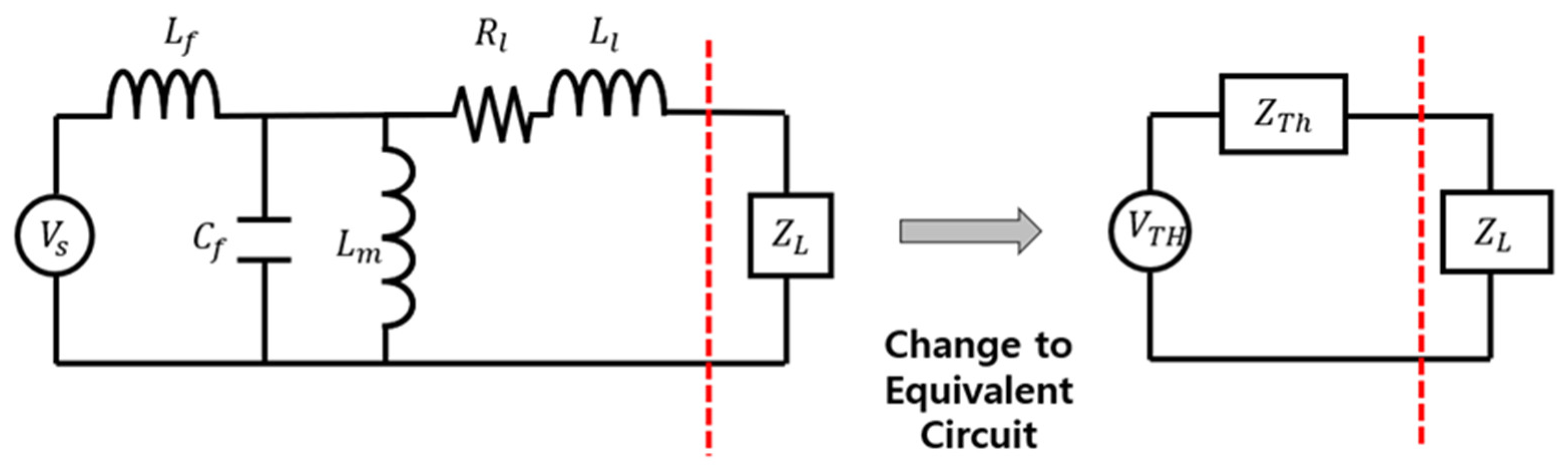
For the mathematical analysis of the SONAR-specific single-system structure in Figure 2, we assume that the battery (DC link) voltage remains constant over time and the inverter linearly outputs the voltage according to the modulation index (MI). This assumption enables us to represent the voltage applied to the LC filter as an equivalent voltage source, Vs. Furthermore, the component parameters within the SONAR amplifier structure (illustrated in Figure 1) can be parameterized, as shown in Table 2. By utilizing the variables from Table 2 and the structure illustrated in Figure 1, we can represent the equivalent circuit of a single system, depicted in Figure 5.
To calculate the Thevenin equivalent circuit voltage and impedance values in Figure 5, the expressions for the voltage across each magnetizing inductance and the equivalent impedance as observed from the load ( Z L ) can be formulated as shown by Equations (1) and (2). In Equation (2), the leakage inductance of the transformer and the parasitic resistance have values that are less than a few percent of the transformer’s magnetizing inductance [20,21,22]; thus, these parameters can be excluded for simplicity.
V T H = 1 s C f | | ( s L m ) s L f + 1 s C f | | ( s L m ) V s = L m s 2 L m L f C f + L m + L f V s
Z T H = R s + s L l s + s L f | | 1 s C f | | ( s L m ) = R l + s L l + + s L m L f s 2 L m L f C f + ( L m + L f )   s L m L f s 2 L m L f C f + ( L m + L f )
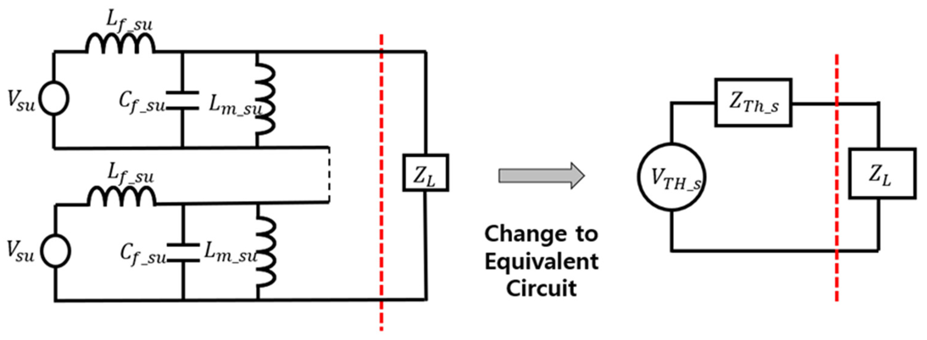
Following a procedure similar to the derivation of the equations for the single-system circuit shown in Figure 5, the equations for the serial system were also derived using variables, as listed in Table 3. It was assumed that there were no variations in the design parameters between the serial modules, and the DC link voltage was assumed to be supplied in parallel from a DC power source.
Similar to the process outlined in Figure 5, the Thevenin equivalent circuit shown in Figure 6 can be formulated as shown by Equations (3) and (4).
V T H s u = n 1 s C f s u | | s L m s u s L f s u + 1 s C f s u | | s L m s u V s = L m _ s n s 2 L m _ s u L f _ s u C f _ s u + ( L m _ s u + L f _ s u ) ( n V s )
      Z T H _ s u = n ( s L f _ s u ) | | ( 1 s C f _ s u ) | | ( s L m _ s u ) = s L m s u ( n L f s u ) s 2 L m _ s u L f _ s u C f _ s u + ( L m _ s u + L f _ s u ) .
The electrical characteristics of the single system illustrated in Figure 2 and serial system in Figure 3 must be identical. Therefore, Equations (2) and (4) should be identical. To establish this equivalence, we derived the relationships between the component parameters of the serial and single systems, yielding Equation (5). In Equation (5), the resistances and inductances are divided by the number of modules in the serial configuration, and the capacitance in the serial system is equal to the capacitance of a single system multiplied by the number of modules.
L s u = L n ,   R s u = R n ,   C s u = n C
From the results of Equation (5), it follows that the voltage of the Thevenin equivalent circuit should be equal to the voltage of the single system; consequently, the relationship between the two voltages and the number of serial modules is expressed as
V s u = V s n .

2.4. Extracting Design Parameters for High-Power Amplifiers

Before proceeding with the derivation of the design parameters for the high-power amplifier of the single system using the design procedure shown in Figure 4, the number of serial modules in the serial system is determined using the voltage transfer function formula. The symbols and definitions of the variables used to derive the voltage transfer function formula are presented in Table 4 and Figure 7.
To derive the voltage transfer function formula, certain values among the variables of the high-power amplifier were fixed according to the specified requirements, as shown in Table 5.
Among the values used to derive the design parameters for both the single system and individual modules, the capacity of the high-power amplifier, operating frequency range of the FFR sensor, DC link voltage, selected MI for controllability, and inverter switching frequency were fixed as control variables. Additionally, the variables in Table 4 that can be expressed as relationships with the control variables are categorized as dependent variables, reducing the types of variables introduced in both tables. The control variables and dependent variables can be mathematically expressed by (7)–(12).
V p r i _ s y s = V p r i _ u n i t = V D C · M I 2
a u n i t N 2 n N 1 1500 n V p r i _ u n i t
I r a t e _ u n i t =   S V p r i _ u n i t · n =   S · 2 V D C · M I · n
I m _ u n i t = I r a t e _ u n i t × x 100 = S · 2 V D C · M I · n × x 100
L m = V p r i _ u n i t 2 π · f f u n · I m _ u n i t = V p r i _ u n i t 2 π · f f u n · I r a t e _ u n i t × x 100
L l = L m × y 100 = V p r i u n i t 2 π · f f u n · I m u n i t × y 100 = V p r i _ u n i t 2 π · f f u n · I r a t e _ u n i t × x × y
According to the dependent variables, the voltage transfer function relative to the primary-side voltage of the transformer compared with the voltage applied to the SONAR sensor can be formulated as shown by Equation (13). When converted from a complex form to a magnitude, Equation (14) is obtained. The equation expresses the relationship in terms of the load impedance magnitude, number of serial modules, ratio of rated current to magnetizing current, and ratio of magnetizing inductance to leakage inductance. The impedance values were determined based on the sensor impedance at the frequency corresponding to the highest load. The leakage inductance ratio was selected as 1% considering the worst-case scenario based on transformer manufacturing approaches [22]. The results for the voltage transfer as a function of n and x are shown in Figure 8.
V o u t V p r i _ u n i t = Z L · j X m j X l · Z L + j X m · Z L + j X m · j X l = Z L · j X m j X l · Z L + j X m · Z L + ( a u n i t ) 2 · j X m · j X l = y 100 + 1 · ( R L 2 + X L 2 ) + 1500 2 · y S · n · x ( X L + j R L ) { y 100 + 1 · Z L } 2 + ( 1500 2 · y S · n · x ) 2 + 2 · X L · y 100 + 1 · 1500 2 · y S · n · x
m a g ( V o u t V p r i _ u n i t )     Z L y 100 + 1 ) 2 · ( Z L 2 + 2 · y 100 + 1 · 45 · y · X L n · x + ( 45 · y n · x ) 2 { y 100 + 1 · Z L } 2 + ( 45 · y n · x ) 2 + 2 · X L · y 100 + 1 · 45 · y n · x  
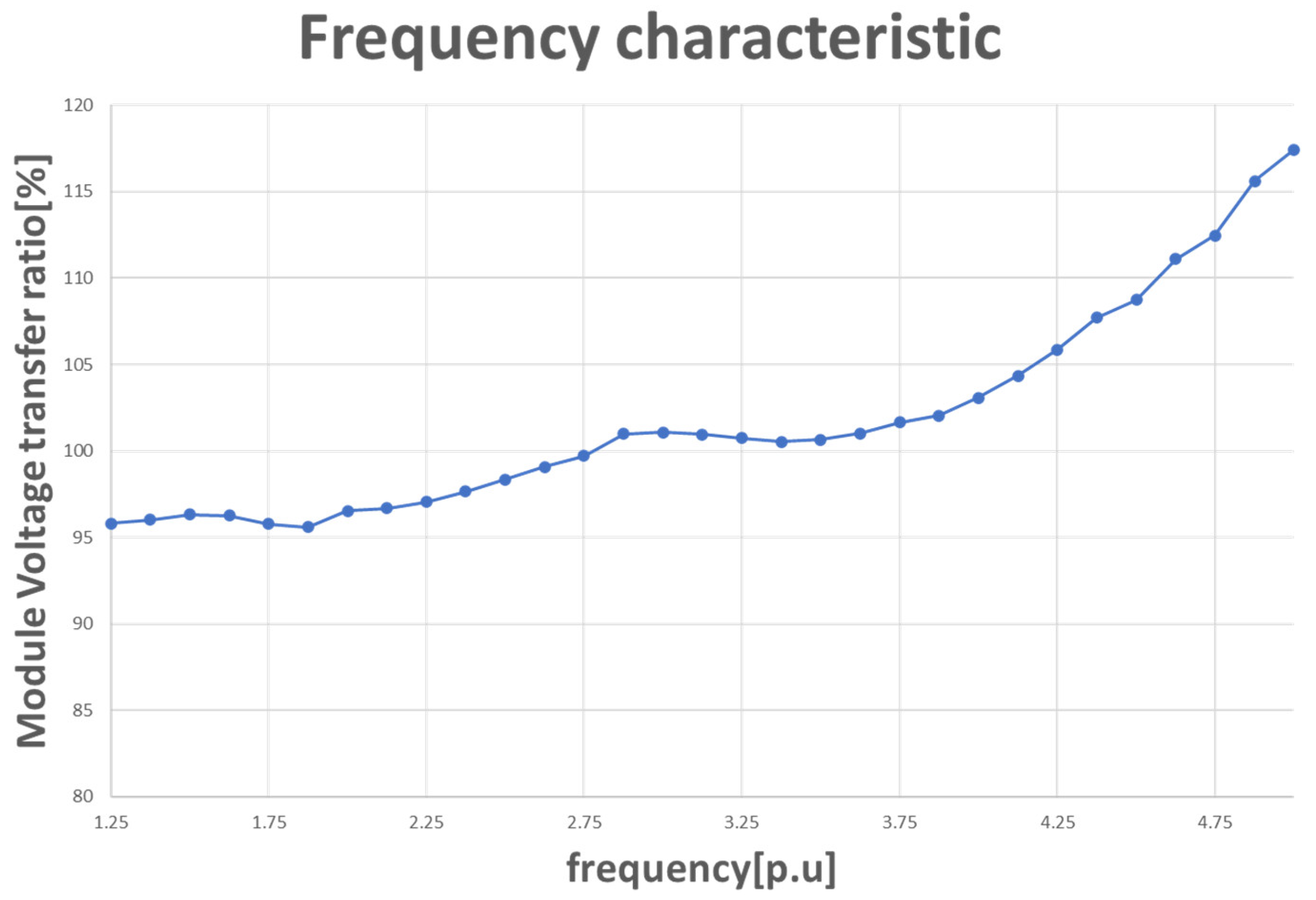
Assuming a ratio of the rated current to the magnetizing current (x) of approximately 5% in Equation (14), the voltage transfer ratio with respect to the number of serial modules is shown in Figure 9. Among these values, the number of serial modules was selected according to the point at which the change in voltage transfer became less significant with the variation in the number of serial modules; this occurred at 10 serial modules. Therefore, the number of serial modules was selected as a design parameter.

2.5. Derivation of LC Filter Parameters

To generate the AC voltage and perform impedance matching, LC filters and transformers are primarily designed using two approaches. In the first approach, an equivalent electrical circuit with impedance and phase matching at the matching frequency of the SONAR sensor is derived, and the inductance value for reactive power removal is designed using these parameters. Subsequently, the SONAR load, including the matching transformer, is equivalently transformed into a single resistance, and the LC filter parameters are derived to match the cutoff frequency [15]. However, this approach does not consider the parasitic elements within the LC filter and matching transformer, which leads to discrepancies between the design characteristics and actual performance. Thus, an approach was recently proposed that involves the simultaneous design of LC filters and matching transformers, considering the parasitic elements within both components [7]. Therefore, in this study, the design of LC filters for a single system was considered a parasitic parameter. 
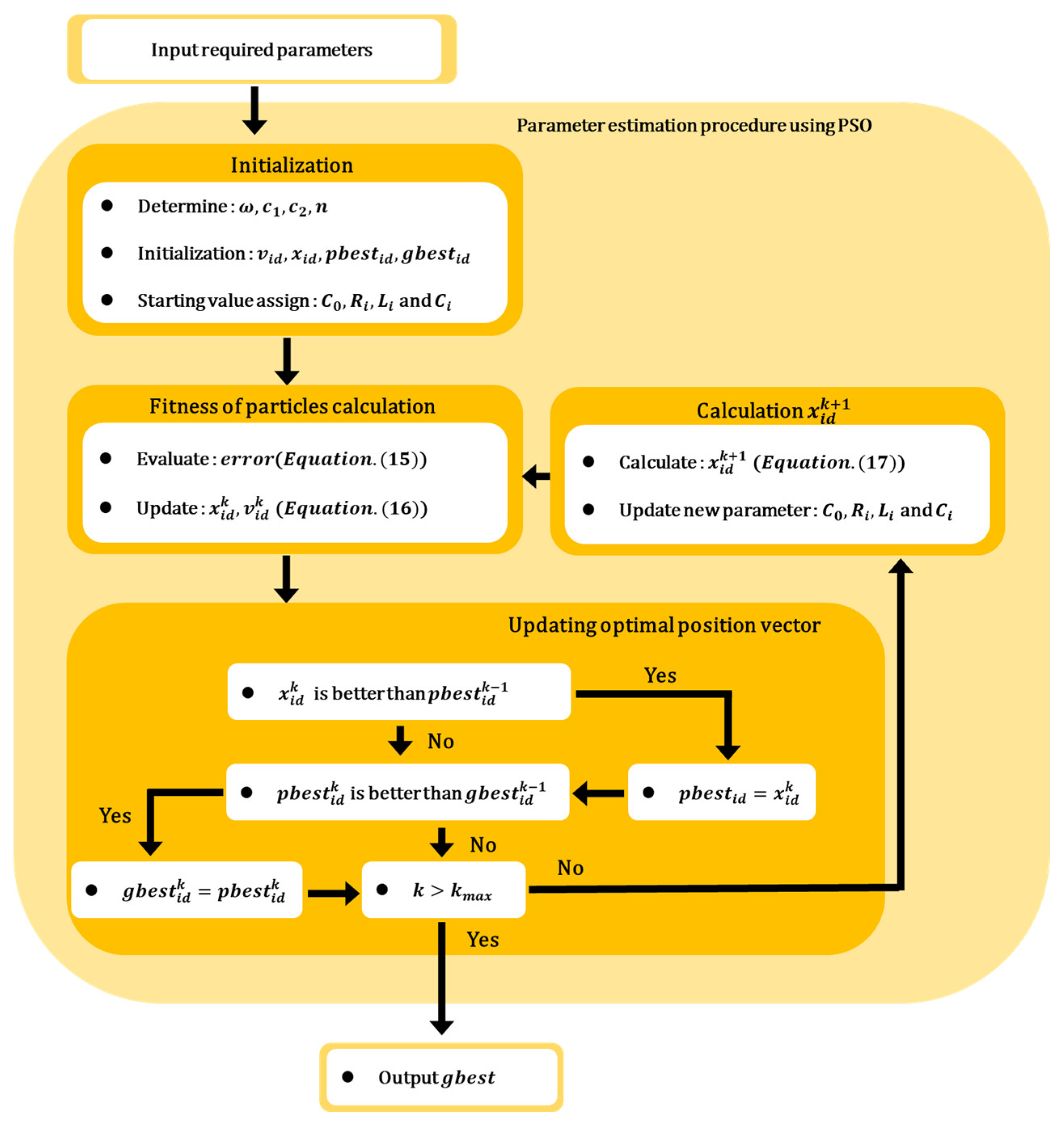
Figure 10 and the following particle swarm optimization (PSO) algorithm procedure and equations were used to derive the parameters in Table 6:
(1) Initialization phase: The necessary variables for the PSO algorithm were initialized, and the initial values were set.
(2) Fitness calculation of the particles: The impedance characteristics of the sensor were calculated using the estimated parameter values of the equivalent circuit and the variables obtained from the previous step. The calculated and measured impedance characteristics were compared to evaluate the error level. The evaluation was performed using Equation (15), where e represents the error value; k m a g and k p h a s e represent the weighting factors for the magnitude and phase errors, respectively; and Z m a g and Z p h a s e represent the errors in the estimated impedance magnitude and phase, respectively.
e = k m a g Z m a g + k p h a s e Z p h a s e
(3) p b e s t i d k and g b e s t i d k update phase: The evaluation values of each particle, as determined by the fitness function, were compared with the previously recorded best evaluation value p b e s t i d k . If the current evaluation value is lower than the previous best evaluation value, the parameter values were updated and assigned a new p b e s t i d k . Subsequently, among all the updated p b e s t i d k values, the one with the best evaluation result, that is, g b e s t i d k , was compared with the previous best evaluation result within the swarm. If the new evaluation result is superior, the derived parameters are updated. Once all the updates were completed, the algorithm checked whether the maximum number of iterations had been reached or whether the evaluation result satisfied the termination criterion. If either condition was satisfied, the PSO algorithm was terminated. The process ensured that the particles continuously updated their personal best positions and velocities with consideration of the global best position within the swarm.
(4) x i d k + 1 calculation phase: In this phase, when the maximum number of iterations was not exceeded and the evaluation result did not satisfy the termination criterion, new parameter values ( x i d ) were assigned for the next optimization operation. The new parameter values were determined using the PSO algorithm, as shown in Equation (16). The velocity change ( v i d ), which indicated the direction and magnitude of the particle movement, was added to the current x i d value, resulting in the derivation of the new x i d value, as shown in Equation (17). This calculation phase ensured that each particle updated its position based on its previous position and the velocity change determined by the PSO algorithm, enabling continuous exploration and refinement of the parameter space in the search for an optimal solution.
V i d k + 1 = w V i d k + c 1 r i k p b e s t i d k x i d k + c 2 r 2 k g b e s t d k x i d k
x i d k + 1 = x i d k + V i d k + 1
The parameters obtained through the aforementioned procedure for satisfying the maximum harmonic distortion criteria imposed on the SONAR, along with a comparison between the baseline voltage transfer function and parameter optimization results, are presented in Table 7.
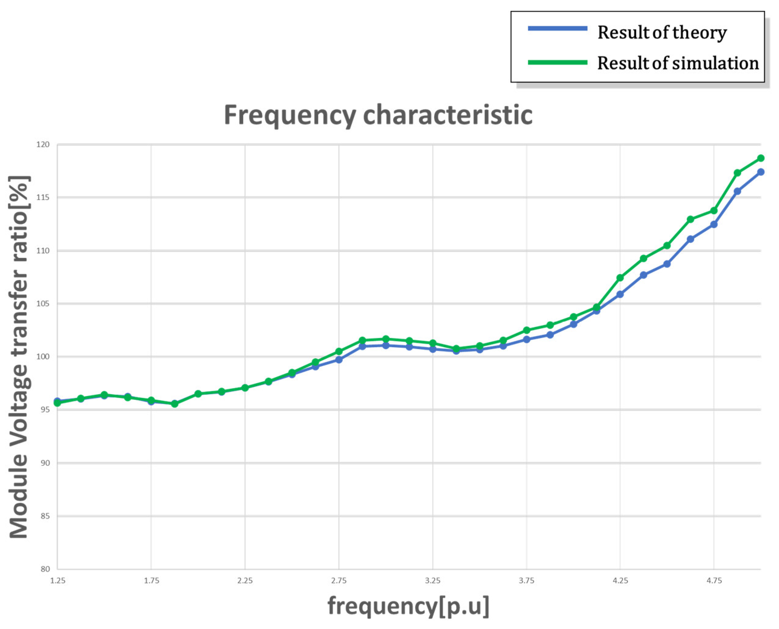
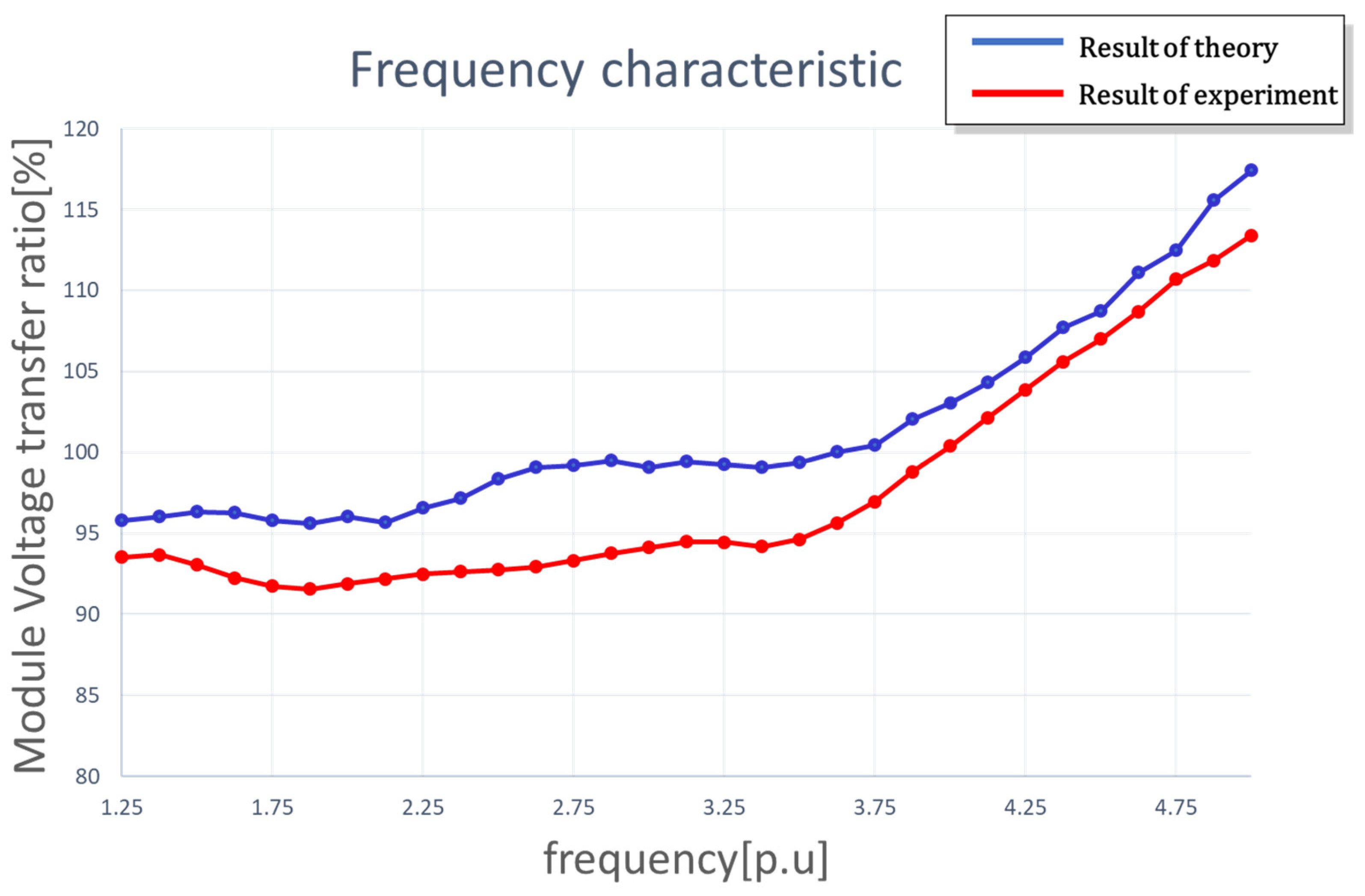
The design parameters of the modules obtained through the proposed high-power amplifier design procedure shown in Figure 4 are presented in Table 8. The voltage transfer characteristics of the parameters obtained using the proposed procedure within the SONAR load-operating bandwidth are shown in Figure 11.

2.6. Derivation of Reduced-Capacity Amplifier Design Parameters

Simulations and experiments were conducted to validate the proposed high-power amplifier design. However, owing to the constraints in manufacturing, safety, and testing equipment for a 50 kVA high-power amplifier, a reduced-capacity parameter set with the same frequency characteristics was used for validation. The design procedure for the reduced-capacity amplifier followed the per-unit (p.u.) method shown in Figure 12.
(1)
The design parameters of the unit module were derived using the proposed procedure.
(2)
Based on the aforementioned parameters, a fundamental value and p.u. value were set for electrical characteristics, such as the voltage, current, and impedance of the amplifier at one frequency within the SONAR operating frequency range.
(3)
To minimize changes in the amplifier characteristics with frequency variations, the turn ratio of the transformer was fixed, and the change in voltage gain with respect to the number of modules was adjusted through DC link voltage control using the results of Equation (6).
(4)
Finally, the basic values suitable for the reduced capacity were selected, and the reduced-capacity parameters were rederived.
The design parameters for the reduced-capacity amplifier were obtained using the procedure shown in Figure 12 and presented in Table 9. The frequency–voltage transfer function characteristics were compared to the amplifier characteristics before and after the capacity reduction based on the procedure, as shown in Figure 13. The average error rate was confirmed to be 0.19%, verifying that there were no problems with the high-power amplifier design procedure based on the characteristics of the reduced capacity.

3. Simulation

The aforementioned procedure confirmed that the average error between the characteristics of the reduced-capacity amplifier based on the unit method and those obtained using the proposed high-power amplifier design procedure is within 1%. Accordingly, in this study, simulations were conducted with reduced-capacity parameters and experimentally validated to verify the design procedure for the proposed high-power amplifier.
The simulation setup parameters for the SONAR amplifier are presented in Table 10, and the overall configuration is depicted in Figure 14. The simulation involved four serial modules. On the right side of the amplifier, an electrical equivalent load was derived from the SONAR characteristics within the operating frequency range.
Using the simulation environment described in Figure 14, the theoretical design procedure was validated by comparing the voltage transfer function within the operating frequency range between the formula-based operating frequency and the simulation results, as shown in Figure 15.
According to the simulation parameters listed in Table 10, the simulation environment shown in Figure 14 was constructed. The voltage transfer function characteristics of the amplifier within the operating frequency range of the SONAR sensor were compared between the theoretical and simulation results. For this comparison, the voltage transfer characteristics at different frequencies were plotted, as shown in Figure 15, and the maximum error for each frequency ( e m a x ) and the average error within the operating frequency range ( e a v g ) were calculated. The theoretical and simulation results are compared in Table 11.

4. Experimental Setup and Verification

The percentage errors between the values of the LC filter and transformer inductance obtained through the aforementioned procedure and their reference values are presented in Table 12. The maximum error rate was 1.3%, and the average error rate was <2% for each parameter. Thus, design parameters aligned closely with the actual manufacturing specifications. According to these parameters, an experimental setup similar to that of the previous simulation, as shown in Figure 16, was configured to validate the simulation in the form of a voltage transfer function concerning the frequency applied to the SONAR equivalent load.
As indicated by the LC filter and transformer parameters presented in Table 12, in the experiment, the basic parameters, such as the switching frequency and DC link voltage, were consistent with those listed in Table 10. As shown in Figure 16, the experimental setup consisted of an electrical equivalent circuit load with characteristics similar to those of the SONAR operating band, a high-power amplifier designed using the proposed method, DC power supply, controller, and the required power devices. In the experiment, the root-mean-square (RMS) value and frequency magnitude of the voltage applied to the SONAR equivalent load were measured and compared to verify that the desired voltage frequency and magnitude were successfully delivered.
Figure 17 presents the results for the RMS voltage applied to the SONAR equivalent load at different frequencies within the experimental setup depicted in Figure 16. According to these results, the average error ( e a v g ) and maximum error ( e m a x ) were calculated and compared with the theoretically derived output-voltage characteristics of a single module, as indicated in Table 13. The proposed amplifier characteristics are reflected with an average error within 5%, considering the parasitic resistance and parameter variations.

5. Conclusions

A design procedure for high-power amplifiers to drive SONAR systems in response to the increasing power requirements of SONAR operation was developed and validated through simulations and experiments. Traditionally, power amplifiers and associated components, such as LC filters and matching transformers, have been designed and fabricated as single-power converters ranging from a few watts to kilowatts. However, the operational power is increasing; thus, we proposed a different approach. Instead of using a single-power converter, a power amplifier topology comprising multiple serially connected power converters is employed. The goal was to minimize the variations in voltage characteristics with changing operating frequencies, select the optimal number of serial modules, consider impedance matching, and design an LC filter to attenuate harmonics for SONAR operation at specific frequencies.
To validate the proposed approach, simulations based on the obtained design parameters and experiments with a reduced capacity were conducted to compare the voltage-transfer characteristics of the amplifier across different frequencies. Compared with the theory, the simulations exhibited average and maximum errors of 0.6% and 1.8%, respectively. The average and maximum errors between the results of the theoretical analysis and the reduced-capacity experiment were 3.79% and 6.19%, respectively.
The proposed amplifier design approach was validated to exhibit a level of error comparable to the conventional amplifier design technique, with an error rate of 3.9% in comparison at Table 14. This validation was performed using the terminology commonly employed in electrical engineering journal papers.
We anticipate that serial systems that reflect the characteristics of a single system can be designed using the procedure presented in this study.

Author Contributions

Conceptualization, J.C.; Methodology, J.J. and J.C.; Software, J.J.; Validation, J.J. and J.C.; Formal analysis, J.J.; Investigation, J.J.; Data curation, J.J.; Writing—original draft, J.J.; Writing—review & editing, H.M. and J.C.; Visualization, J.J.; Supervision, H.M. and J.C.; Project administration, H.M.; Funding acquisition, D.L. All authors have read and agreed to the published version of the manuscript.

Funding

This research was supported by Agency for Defense Development (The Study of high power amplification techniques for FFR suitable for CAS transmission).

Data Availability Statement

The data presented in this study are available on request from the corresponding author. The data are not publicly available due to security reason.

Conflicts of Interest

Authors Jejin Jang and Jaehyuk Choi were employed by the company Tin Technology Co., Ltd. The remaining authors declare that the research was conducted in the absence of any commercial or financial relationships that could be construed as a potential conflict of interest.

References

  1. Suresh, Y.; Venkataramanaiah, J.; Panda, A.K.; Dhanamjayulu, C.; Venugopal, P. Investigation on cascade multilevel inverter with symmetric, asymmetric, hybrid and multi-cell configurations. Ain Shams Eng. J. 2017, 8, 263–276. [Google Scholar] [CrossRef]
  2. Kumar, P.A.; Ramesh, P. Comparison of Different Multilevel Converter Strategy for Induction Motor Drive Application. Int. J. Recent. Innov. Trends Comput. Commun. 2014, 2, 1887–1893. [Google Scholar]
  3. Choudhury, S.; Bajaj, M.; Dash, T.; Kamel, S.; Jurado, F. Multilevel Inverter: A Survey on Classical and Advanced Topologies, Control Schemes, Applications to Power System and Future Prospects. Energies 2021, 14, 5773. [Google Scholar] [CrossRef]
  4. Babaei, E.; Alilu, S.; Laali, S. A new general topology for cascaded multilevel inverters with reduced number of components based on developed H-bridge. IEEE Trans. Ind. Electron. 2014, 61, 3932–3939. [Google Scholar] [CrossRef]
  5. Mariusz, M.; Gopakumar, K.; Jose, R.; Marcelo, P.A. A survey on cascaded multilevel inverters. IEEE Trans. Ind. Electron. 2010, 57, 2197–2206. [Google Scholar]
  6. Wu, J.-C.; Wu, K.-D.; Jou, H.-L.; Xiao, S.-T. Diode-clamped multi-level power converter with a zero-sequence current loop for three-phase three-wire hybrid power filter. Electr. Power Syst. Res. 2011, 81, 263–270. [Google Scholar] [CrossRef]
  7. Choi, J.-H.; Mok, H.-S. Simultaneous Design of Low-Pass Filter with Impedance Matching Transformer for SONAR Transducer Using Particle Swarm Optimization. Energies 2019, 12, 4646. [Google Scholar] [CrossRef]
  8. Song, S.M.; Kim, I.D.; Lee, B.H.; Lee, J.M. Design of Matching Circuit Transformer for High-Power Transmitter of Active Sonar. J. Electr. Eng. Technol. 2020, 15, 2145–2155. [Google Scholar] [CrossRef]
  9. Choi, J.; Lee, D.H.; Mok, H. Discontinuous PWM Techniques of Three-Leg Two-Phase Voltage Source Inverter for Sonar System. IEEE Access 2020, 8, 199864–199881. [Google Scholar] [CrossRef]
  10. Jang, J.J.; Choi, J.H.; Lee, D.H.; Mok, H.S. Estimation Method of an Electrical Equivalent Circuit for Sonar Transducer Impedance Characteristic of Multiple Resonance. Sensors 2023, 23, 6636. [Google Scholar] [CrossRef] [PubMed]
  11. Oh, Y.S. Development of High Resolution Side Scan Sonar System Using Multi Beam Array Porcessing. Ph.D. Thesis, Department of Ocean Engineering Graduate School of Korea Maritime University, Busan, Republic of Korea, 2012. [Google Scholar]
  12. Kim, H.E. Torpedo Defense System Research Using HMS (Hull Mount Sonar) of PCC (Patrol Combat Corvette). Master’s Thesis, Department of Electronic Graduate School of Ajou University, Suwon, Republic of Korea, 2012. [Google Scholar]
  13. Haneum, O. Development of Acoustic Transmission Model of SONAR with FFR Transducers and Its Application. Ph.D. Thesis, School of Mechanical Engineering, The Graduate School Pusan National University, Busan, Republic of Korea, 2020. [Google Scholar]
  14. Im, J.B.; Yoon, H.W.; Kwon, B.J.; Kim, H.S.; Lee, J.M. Analysis and verification of the characteristic of a compact free-flooded ring transducer made of single crystals. J. Acoust. Soc. Korea 2022, 41, 278–286. [Google Scholar]
  15. Song, S.M.; Kim, I.D.; Lee, B.H.; Lee, J.M. Design of transformer with impedance matching circuit for high power transmitter of active sonar. In Proceedings of the 2019 10th International Conference on Power Electronics and ECCE Asia (ICPE 2019-ECCE Asia), Busan, Republic of Korea, 27–30 May 2019; pp. 2126–2131. [Google Scholar]
  16. Park, S.U. Passive Element Optimal Design Method for Wideband Sonar Sensor Driving Circuit. Ph.D. Thesis, School of Electrical Engineering The Graduate School Konkuk University, Seoul, Republic of Korea, 2022. [Google Scholar]
  17. Sreekumar, A.; Panchalai, V.N.; Chacko, B.P.; Thekkath, P. Multilevel converter for excitation of underwater transducers. In Proceedings of the 2015 International Conference on Advances in Computing, Communications and Informatics (ICACCI), Kochi, India, 10–13 August 2015; pp. 651–655. [Google Scholar] [CrossRef]
  18. Chacko, B.P.; Panchalai, V.N.; Sivakumar, N. Multilevel digital sonar power amplifier with modified unipolar SPWM. In Proceedings of the 2015 International Conference on Advances in Computing, Communications and Informatics (ICACCI), Kochi, India, 10–13 August 2015; pp. 121–125. [Google Scholar] [CrossRef]
  19. Rajesh, C.R.; Meenalochini, P.; Kannaiah, S.K.; Bindu, A. A hybrid control topology for cascaded H-bridge multilevel inverter to improve the power quality of smart grid connected system: NBO-RERNN approach. Expert Syst. Appl. 2024, 238, 122054. [Google Scholar] [CrossRef]
  20. Bin, C. Design optimisation of an inductor-integrated MF transformer for a high-power isolated dual-active-bridge DC–DC converter. IET Power Electron. 2019, 12, 2912–2922. [Google Scholar] [CrossRef]
  21. Payne, A. Skin Effect, Proximity Effect and the Resistance of Circular and Rectangular Conductors. 2016. Available online: https://coil32.net/files/Alan_Payne/Skin-Effect-Proximity-Loss-and-the-Resistance-of-Circular-and-Rectangular-ConductorsIssue-4.pdf (accessed on 10 December 2022).
  22. Fouineau, A.; Raulet, M.-A.; Lefebvre, B.; Burais, N.; Sixdenier, F. Semi-Analytical Methods for Calculation of Leakage Inductance and Frequency-Dependent Resistance of Windings in Transformers. IEEE Trans. Magn. 2018, 54, 1–10. [Google Scholar] [CrossRef]
Figure 1. SONAR transducer power amplifier—system diagram [10].
Energies 17 01581 g001
Figure 2. Unified system architecture of the high-power amplifier for SONAR.
Energies 17 01581 g002
Figure 3. Cascaded system architecture of the high-power amplifier for SONAR.
Energies 17 01581 g003
Figure 4. Proposed power amplifier design procedure.
Energies 17 01581 g004
Figure 5. Thevenin equivalent circuit of the unified amplifier system.
Energies 17 01581 g005
Figure 6. Thevenin equivalent circuit of the cascaded amplifier system.
Energies 17 01581 g006
Figure 7. Variable definition for the cascaded high-power amplifier.
Energies 17 01581 g007
Figure 8. Voltage divider ratio (at y = 1%).
Energies 17 01581 g008
Figure 9. Relationship between the number of unit modules and the voltage divider ratio.
Energies 17 01581 g009
Figure 10. Parameter estimation process of the PSO algorithm [10].
Energies 17 01581 g010
Figure 11. Power amplifier frequency characteristics.
Energies 17 01581 g011
Figure 12. Re-extraction procedure for the reduced capacity amplifier.
Energies 17 01581 g012
Figure 13. Comparison of voltage transfer function characteristics between a 50 kVA amplifier and a 2 kVA amplifier.
Energies 17 01581 g013
Figure 14. Simulation configuration of the SONAR amplifier.
Energies 17 01581 g014
Figure 15. Comparison of the voltage transfer characteristics between the theory and simulation.
Energies 17 01581 g015
Figure 16. Setup for the power amplification experiment.
Energies 17 01581 g016
Figure 17. Comparison of voltage transfer function characteristics between the theory and experiment.
Energies 17 01581 g017
Table 1. Characteristics of different types of SONAR sensors.
Sensor TypePowerOperating RangeSimplicity of StructureHydraulic PressureEfficiency
TonpilzMiddleLowMiddleMiddleHigh
FlextensionnalMiddleMiddleHighMiddleHigh
FFRHighMiddleMiddleMiddleHigh
Table 2. Variables of unified amplifier system.
SymbolDefinition
V s Supply voltage
L f ,   C f LC filter parameters
(LC filter inductance, LC filter capacitance)
L m ,   R l ,   L l Matching transformer parameters
(Magnetizing inductance, leakage resistance, leakage inductance)
Z L Electrical impedance of SONAR
V t h Voltage source of Thevenin equivalent circuit
Z t h Impedance of Thevenin equivalent circuit
Table 3. Variables of cascaded amplifier system.
SymbolDefinition
V s u Supply voltage
L f _ s u ,   C f _ s u LC filter parameters
(LC filter inductance, LC filter capacitance)
L m _ s u ,   R l _ s u ,   L l _ s u Matching transformer parameters
(Magnetizing inductance, leakage resistance, leakage inductance)
Z L Electrical impedance of SONAR
V t h _ s Voltage source of Thevenin equivalent circuit
Z t h _ s Impedance of Thevenin equivalent circuit
n Number of unit modules
Table 4. Variables of high-power amplifier.
SymbolDefinition
V D C DC link voltage
M I Inverter modulation index
f s w Inverter switching frequency
f f u n SONAR sensor operating frequency range
S Apparent power of high-power amplifier
V o u t Power amplifier output voltage
V p r i _ s y s , V p r i _ u n i t First-side voltage of transformer of unified system,
First-side voltage of transformer of cascaded system
I r a t e _ u n i t Converter-rated current at unit module
I m _ u n i t Magnetization current at unit module transformer
N 1 Number of turns of 1st winding
N 2 Number of turns of 2nd winding
n Number of unit modules
a u n i t Transformer turn ratio of cascaded system ( N 2 n N 1 )
x Magnetization current percent ratio with rated current
y Leakage inductance percent ratio with magnetizing inductance
Z L SONAR impedance parameter at frequency
Z L Equivalent impedance of SONAR sensor from primary side of transformer
R L /   X L SONAR impedance real/imaginary parameters
Table 5. Value of control variables.
VariablesValueVariablesValue
V D C 350 V f f u n 1.25–3.75 p.u.
M I 0.7 S 50 kVA
f s w 100 kHz V o u t 1500 V r m s
Table 6. Variables of PSO algorithm.
SymbolDefinition
c 1 ,   c 2 Acceleration constants
d Number of swarms
n Total number of parameters to derive PSO results
r 1 ,   r 2 Uniformly distributed random numbers
ω Inertia weight factor
i Number of particles
p n u m Total number of particles in swarm
V i d t Present velocity vector of swarm
V i d t + 1 Next velocity vector of particle
x i d k Present position vector of swarm
x i d k + 1 Next position vector of particle
g b e s t d Optimal position vector of swarm
p b e s t d Optimal position vector of particle
Table 7. Extracted unified system parameters.
ParameterValueParameterValue
L f 44.26 µH C f 339 nF
L m 19.50 mH a u n i t N 1 n N 2 1.083
Table 8. Derived design parameters of unified high-power amplifier.
ParameterValueParameterValue
S 50 kVA L f 44.26 µH
V o u t 1500 V C f 339 nF
f f u n 1.25 p.u. L m 19.50 mH
a u n i t 1.083:1 n 10 EA
Table 9. Parameters re-extracted using per-unit method.
ParameterValueBase ValueRe-Extracted
Parameter
S 50 kVA5 kVA2 kVA
V o u t 1500 V1500 V320 V
V D C 350 V1500 V175 V
L f 44.26 µH6 Ω 44.26 µH
C f 339 nF6 [Ω]339 nF
L m 19.50 mH6 Ω 19.50 mH
n 10 EA10 EA4 EA
a u n i t 1.083:11.083:11.083:1
Table 10. Simulation configuration parameters.
ParameterValueParameterValue
V D C 175 V C f 339 nF
f s w 100 kHz L m 19.50 mH
t d e a d 100 ns n 4 EA
L f 44.26 µH a u n i t 1.083:1
Table 11. Error rate between theory and simulation.
ParameterValueParameterValue
V D C 175 V C f 339 nF
f s w 100 kHz L m 19.50 mH
t d e a d 100 ns n 4 EA
L f 44.26 µH a u n i t 1.083:1
Table 12. Design parameter values, fabrication parameter values, and errors.
CategoryLC Filter
Inductance
LC Filter CapacitanceTransformer
Magnetizing Inductance
ValueError [%]ValueError [%]ValueError [%]
Design value44.26 µH-339 nF-19.50 mH-
Module 143.67 µH1.34341 nF–0.5819.51 mH–0.06
Module 243.79 µH1.06340 nF–0.2919.40 mH0.5
Module 343.70 µH1.26341 nF–0.5819.69 mH–1
Module 443.73 µH1.19340 nF–0.2919.37 mH0.63
Table 13. Average and maximum error rate between theory and experimental results.
ParameterValueParameterValue
e a v g 3.79% e m a x 6.15%
Table 14. Average error rate between conventional design method and proposed design method.
Conventional MethodProposed Method
Error RateValueParameterValue
e a v g 3.9% e a v g 3.79%
Disclaimer/Publisher’s Note: The statements, opinions and data contained in all publications are solely those of the individual author(s) and contributor(s) and not of MDPI and/or the editor(s). MDPI and/or the editor(s) disclaim responsibility for any injury to people or property resulting from any ideas, methods, instructions or products referred to in the content.

