Article

Overlap Time Compensation and Characteristic Analysis for Current Source Photovoltaic Grid-Connected Inverter

1
Jihua Laboratory, Foshan 528251, China
2
Innovation Institute of Industrial Design and Machine Intelligence, Hunan University, Quanzhou 362006, China
3
College of Electrical and Information Engineering, Hunan University, Changsha 410082, China
*
Author to whom correspondence should be addressed.
Energies 2024, 17(7), 1768; https://doi.org/10.3390/en17071768
Submission received: 11 March 2024 / Revised: 31 March 2024 / Accepted: 2 April 2024 / Published: 8 April 2024

Abstract

:
In the current source photovoltaic grid-connected system, to prevent the DC-link inductor from incurring an opening circuit fault, it is necessary to include the overlap time in the switching signals. However, current error and serious harmonic distortion in the inverter-side and grid-side currents are generated, which will cause additional losses and reduce the power quality of the grid, so it is important to compensate for the current error caused by the overlap time. In this paper, the relationship between the nonlinear current errors caused by the overlap time and the AC-side voltage is analyzed. Then, the mathematical expression of the low-order harmonics with losses caused by the overlap time is derived. On this basis, a current error compensation method with a discrete filter of AC-side voltage is proposed. Finally, a simulation and experiment are carried out to verify the correctness and effectiveness of the theoretical analysis and compensation scheme presented in this paper. With an overlap time of 3 μs, the THD of the grid-side current decreases from 5.93% to 1.59% after compensation.

1. Introduction

Solar energy is widely used in the sustainable and environment-friendly power generation field [1]. Due to the simple structure and mature control technology, a voltage source inverter (VSI) is commonly adopted in the photovoltaic (PV) grid-connected system [2]. However, the VSI is a buck inverter, which requires the DC input voltage to be higher than the peak of the AC output voltage [3]. Therefore, on cloudy or rainy days, the output voltage of the PV cells reduces, the operation of the system stops, and the utilization rate decreases [4]. To address the problem that the input voltage is insufficient, the boost converter or the transformer needs to be added [5,6].
Compared with the VSI, the current source inverter (CSI) is a boost inverter [7,8], so only a single-stage CSI can realize the whole process of light utilization from weak to strong [9,10]. The DC-link inductor of CSI is series connected with the PV cells, so the input current is continuous and controllable, which is convenient in realizing maximum power point tracking (MPPT) [11,12]. The CSI is capable of overcurrent protection, so the reliability is higher than that of the VSI [10,13]. Meanwhile, the operation time of the CSI is longer than that of the VSI [14,15]. Based on the above advantages, CSI is more suitable for the PV grid-connected system [16].
To prevent the short circuit fault, the dead time needs to be added during the modulation process in the VSI [17,18]. Since the dead-time causes the distortion of the inverter output voltage and the gird-side current [19], many compensation schemes for VSI have been proposed to suppress the deadtime effect, such as pulse duration compensation [20], average voltage compensation [21], and adaptive harmonic compensation [22]. Different from VSI, the shoot-through is a normal switching state of the CSI, but the open circuit state is not allowed to occur in the CSI; otherwise, high dv/dt will appear in the DC-link inductor and lead to a serious fault in the system. To prevent the open circuit fault in the CSI, it is imperative to introduce a turn-off delay into all switching signals. At this time, two switching signals remain in the on-state simultaneously, and this is named overlap time [23,24,25]. The nonlinear error of the inverter-side current is generated by the overlap time, which leads to the distortion in the grid-side current. However, the harmonic suppression schemes caused by the overlap time for CSI have rarely been reported. In [24], under the consideration of the influence of the snubber capacitor and the parasitic inductor, the dynamic commutation process of CSI during the overlap time is analyzed in detail, but no specific scheme to suppress the overlap time effect has been presented. According to the relations of the AC-side voltages, the positive and negative sawtooth waves are alternately adopted as the carrier wave in [25]; although the number of the overlapping time sequence can be reduced, the overlapping time effect has not been eliminated. Reference [23] proposes a compensation method for the dwell time of the current vectors according to the AC-side voltages. Reference [26] proposes a current feedforward compensation method in two-phase stationary coordinates. However, the above two methods require high voltage sampling accuracy; otherwise, error compensation may occur. In reference [27], an additional switching tube is parallel connected with the inverter bridge and is used to achieve the null vector; when it is turned on, the commutation action of the active vector is completed, so the overlap time can be eliminated. However, this modulation method is complex. For the current source rectifier, a diode is parallel connected with the rectifier bridge in reference [28], when the open circuit occurs during the commutation process, the additional diode can automatically provide a freewheeling circuit for the DC-link current. However, this topology is not suitable for the inverter occasion.
To effectively suppress the harmonic distortion caused by the overlap time, the following work has been completed. First, the relationship between the nonlinear error of the inverter-side current and the AC-side voltages is obtained during the overlap time. Then, the harmonic characteristics of the inverter-side current and the grid-side current are analyzed in detail. On this basis, the compensation method for the overlap time in the dq axis is proposed. Finally, the simulation and experiment are carried out.
This paper is organized as follows. The overlap time generation mechanism for CSI is analyzed in Section 2. Then, the error and harmonics of the inverter-side current generated by the overlap time are derived in Section 3 and Section 4, respectively, and a compensation scheme to suppress the overlap time effect is also proposed in Section 4. Finally, the simulation and experimental verifications are presented in Section 5. The conclusion is drawn in Section 6.

2. Topology, SVPWM Scheme and Overlap Time Generation of CSI

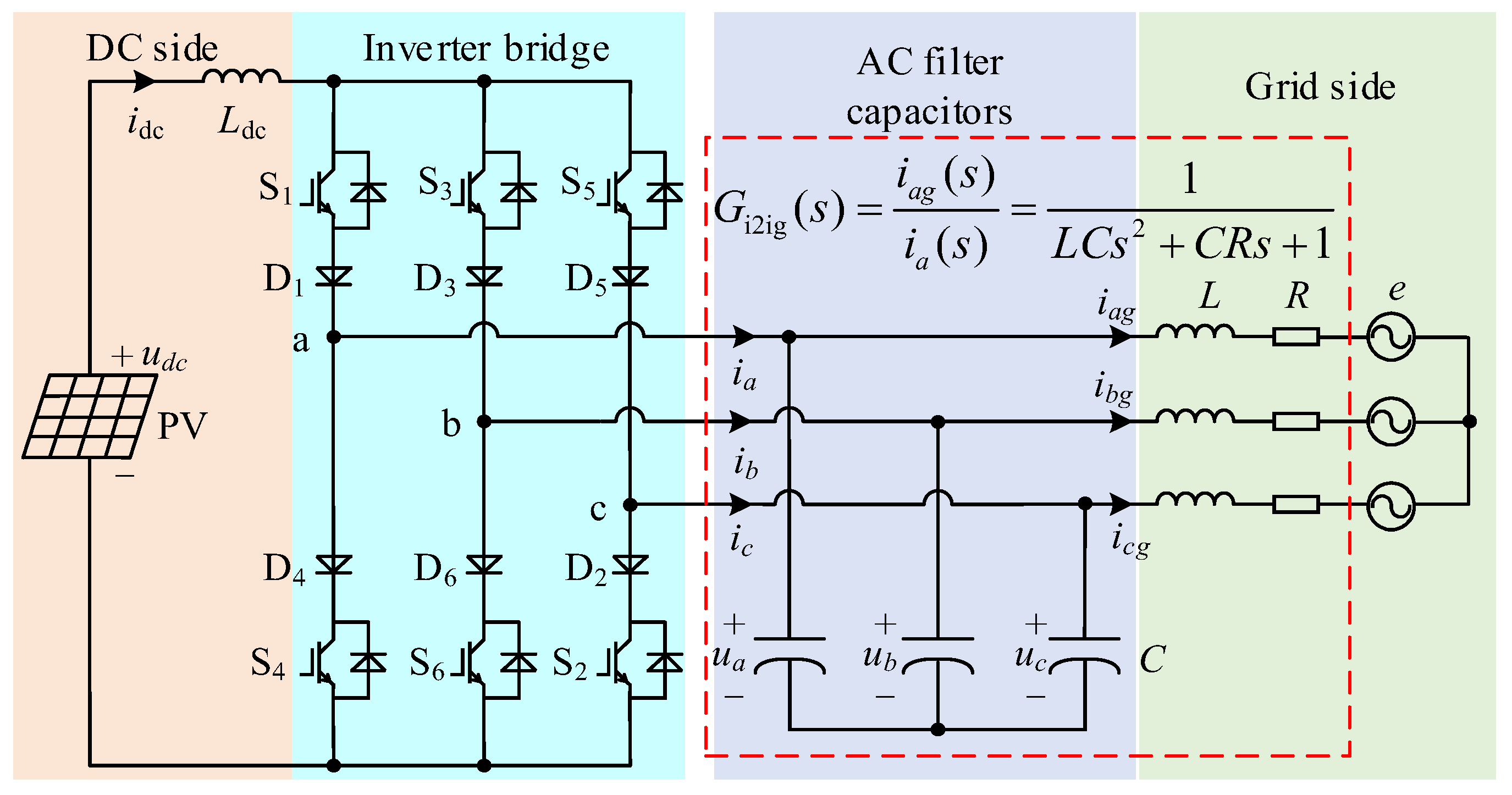
2.1. Topology of CSI

The topology of the current source PV grid-connected inverter is shown in Figure 1, where udc represents the output voltage of the PV cell, Ldc is the DC-link inductor and series connected with the PV cell, and idc is the current of Ldc. The inverter bridge is composed of the switching tubes S1–S6, and diodes D1–D6, C, L, R, and e represent the filter capacitance, inductance, resistance, and grid voltage, respectively. ia, ib, and ic represent the three-phase inverter-side currents; ua, ub, and uc represent the three-phase AC voltage of the inverter; and iag, ibg, and icg represent three-phase grid-side currents.

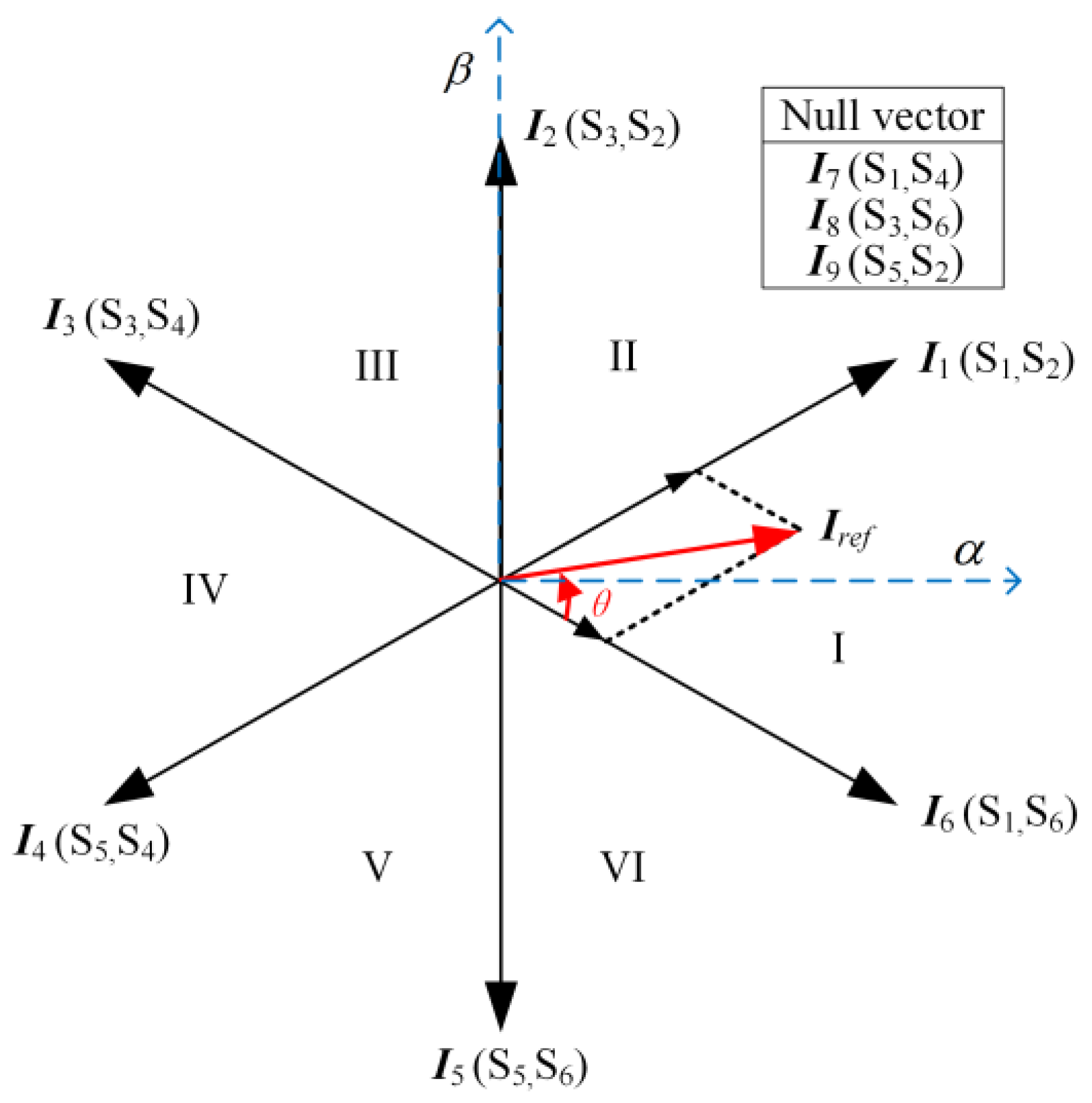
2.2. SVM Scheme of CSI

The current vectors with corresponding switching states are shown in Figure 2. The space is divided into six sectors (I–VI) by the active vectors Ik (k = 1, 2, …, 6). In addition, there are three null vectors: I7, I8, and I9.
Under the common seven-segment sequence SVM based on the triangular carrier wave, the inverter-side current is symmetrical, and the content of the low-order harmonic is less than that under other SVM schemes. If the target vector Iref is located in sector I, Iref is synthesized by the adjacent active vectors (I1 and I6) and null vector I7.
When Iref is located in sector I, the switching signals diagrams are shown in Figure 3a, where ma, mb, and mc are the compared values of the triple commutation time, and p1p6 represent the switching signals of S1–S6, respectively. ‘0’ represents off-state, and ‘1’ represents on-state. At this time, all switching signals of the upper bridge arm (p1, p3, and p5) remain ‘0’ or ‘1’ in a carrier period; commutation occurs among the switching tubes of the lower bridge arm (p2, p4 and p6), and the total number of commutation times is six. t1t6 represent the commutation comments. When Iref is located in sector II, the switching signals diagrams are shown in Figure 3b, and the commutation occurs among the switching tubes of the upper bridge. The solid lines represent the actual signal waveform, and different color dashed lines are used to point out the commutation comments.

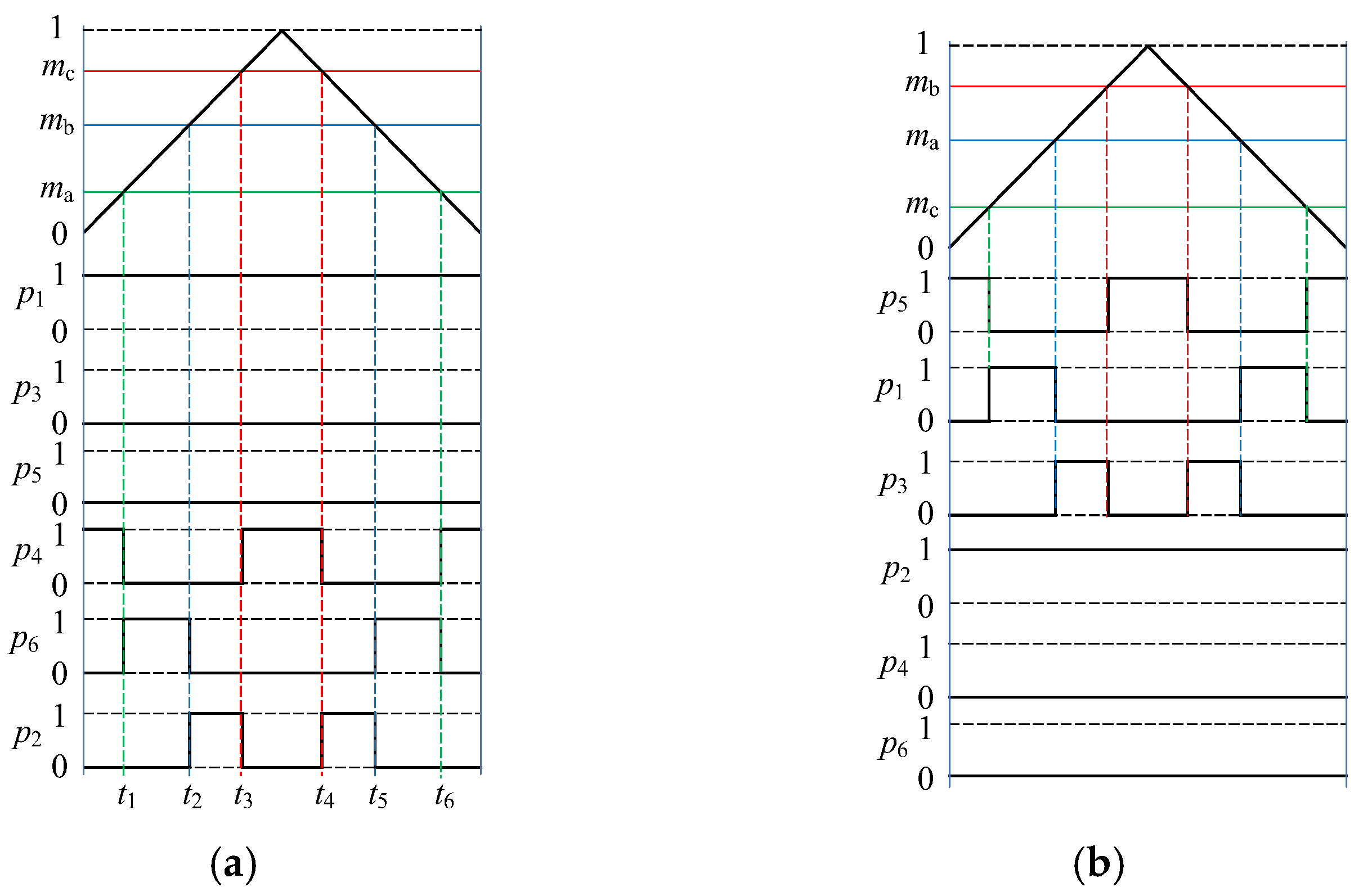
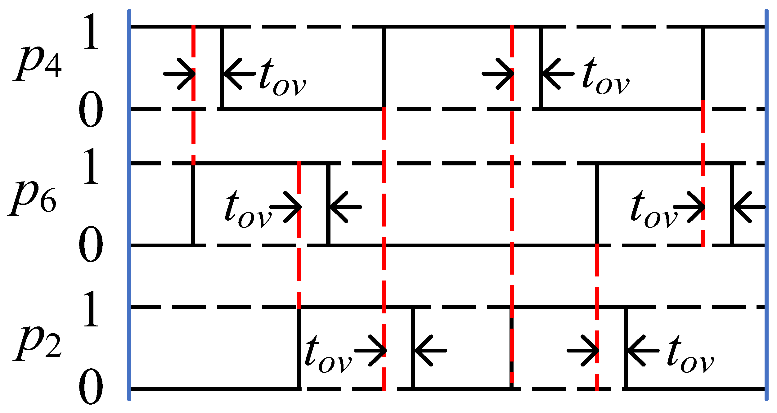
2.3. Overlap Time Generation Mechanism

In Figure 3, the moment of turn-on is consistent with that of turn-off. However, the delay phenomenon exists in the turn-on and turn-off process of the switching tube; if the delay process of turn-off is longer than that of turn-on, a brief open circuit state will appear in the inverter bridge, which will lead to a high dv/dt in the DC-link inductor. Therefore, turn-off delay should be introduced into all switching signals, at this time, the switching signals in the action of Sector I are shown in Figure 4. It can be seen that there are two switching signals in the on-state during tov; this is named the overlap time.

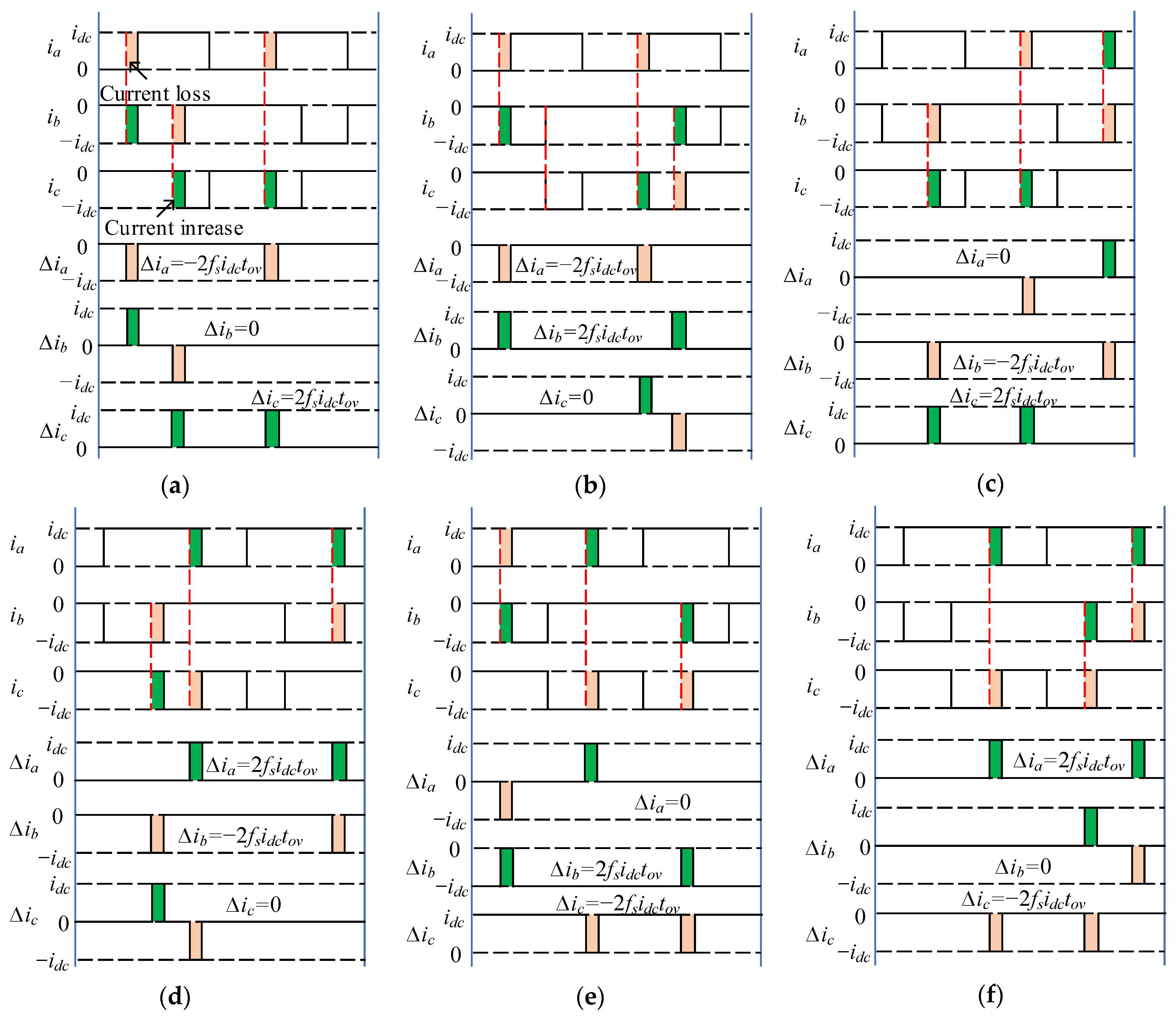
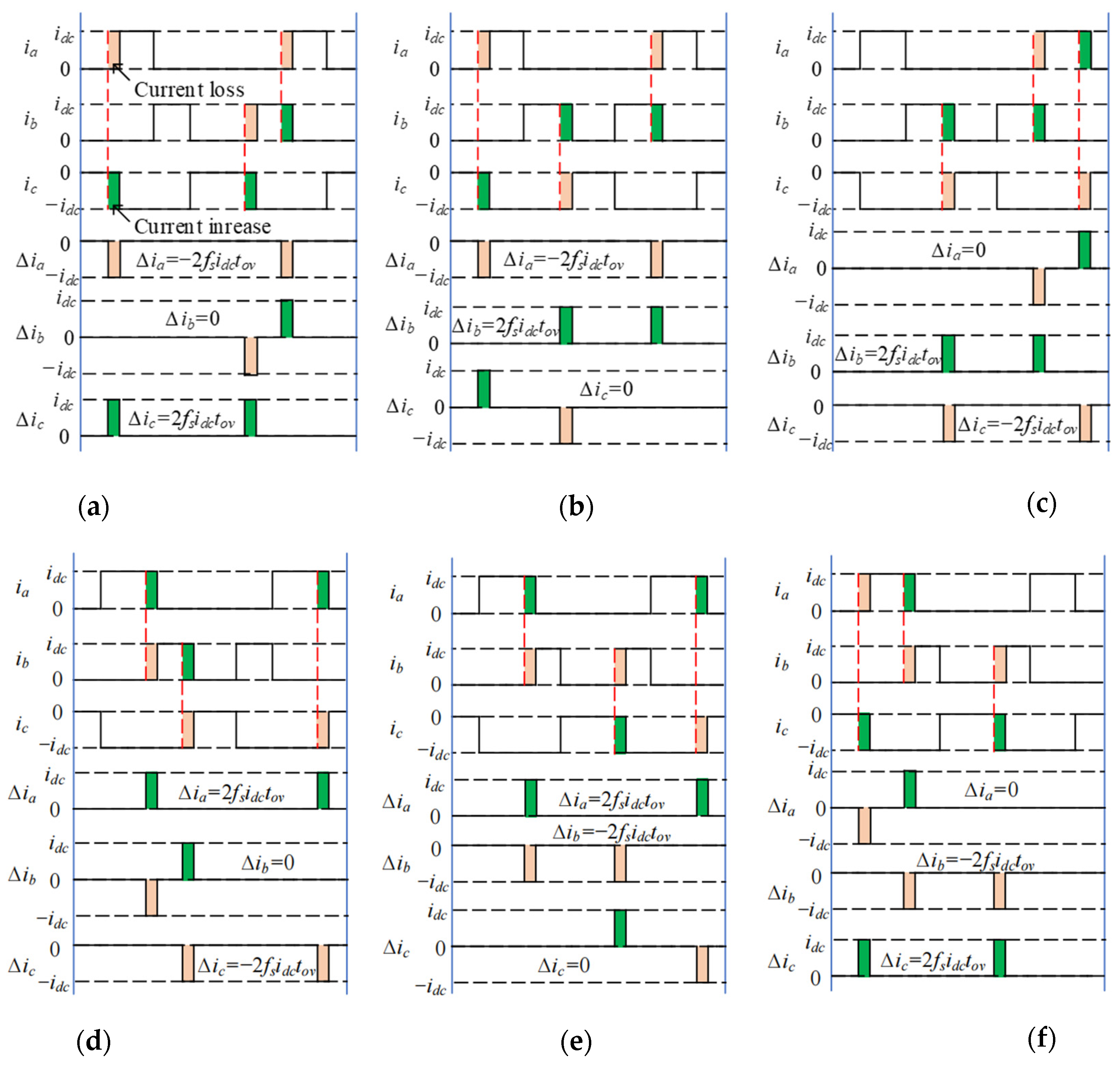
3. Analysis of Overlap Time Effect

In this section, the commutation characteristics during the overlap time are analyzed first; then, the inverter-side current error caused by the overlap time is analyzed.

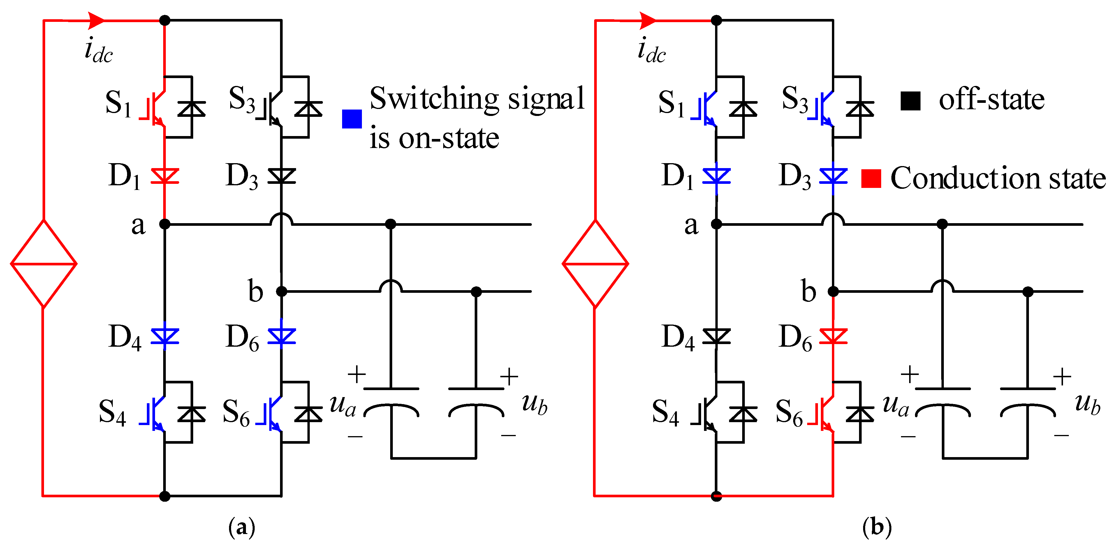
3.1. Commutation Characteristics during the Overlap Time

Figure 5a shows the equivalent circuit during the overlap time in the commutation process from the null vector I7 to the active vector I1. At this time, both S4 and S6 are turned on simultaneously, but the flow path of idc depends on the relation of ua and ub.
If ua > ub, D4 remains in the conduction state, and D6 withstands the reverse voltage; the generated current vector remains I7, which leads to the nonlinear error on ia and ib.
If ua < ub, D4 withstands the reverse voltage, D6 changes to the conduction state, idc is switched from S4 and D4 to S6 and D6, and the generated current vector changes from I7 to I1; commutation can be achieved, and no nonlinear error is generated.
Figure 5b shows the equivalent circuit during the overlap time in the commutation process from the null vector I8 to the active vector I6. At this time, both S1 and S3 are turned on simultaneously, but the flow path of idc also depends on the relation of ua and ub.
If ua > ub, the forward voltage of D3 is higher than D1, so D3 remains in the conduction state, and D1 withstands the reverse voltage; the generated current vector remains I8, which leads to the nonlinear error on ia and ib.
If ua < ub, D3 withstands the reverse voltage, D1 changes to the conduction state, idc is switched from S3 and D3 to S1 and D1, and the generated current vector changes from I8 to I6; no nonlinear error will occur.
The commutation characteristics during the overlap time can be summarized as follows:
  • When the target current vector is located in Sector I, III, or V, the commutation occurs among the lower bridge arms (S4, S6, and S2). DC-link current only flows through the switching tube and diode whose phase voltage is higher, so the nonlinear current will not be generated if the sequence of commutation is from high voltage to low voltage;
  • When the target current vector is located in Sector II, IV, or VI, the commutation occurs among the upper bridge arms (S1, S3, and S5). DC-link current only flows through the switching tube and diode whose phase voltage is lower, so the nonlinear current will not be generated if the sequence of commutation is from low voltage to high voltage.

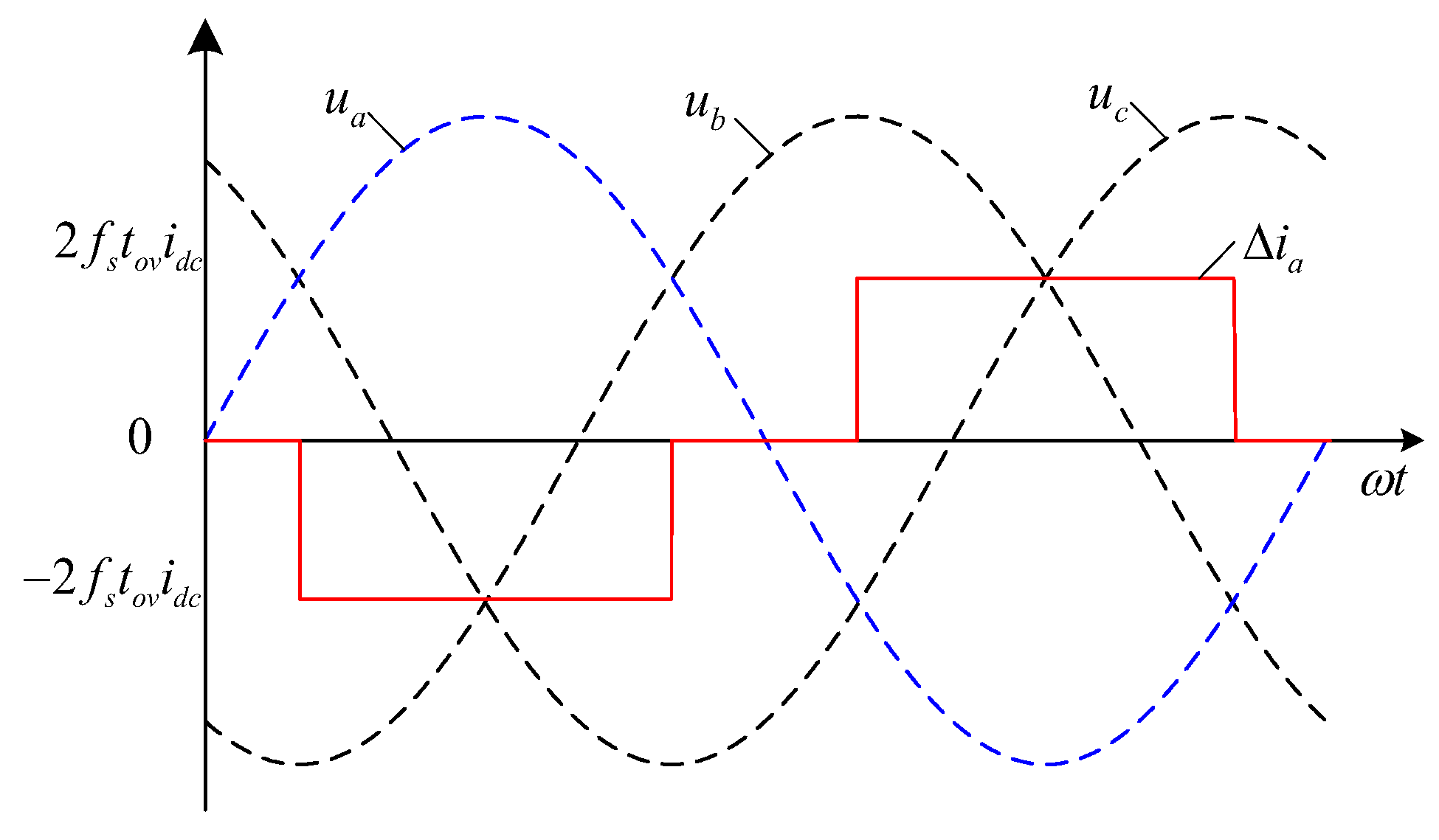
3.2. Current Error Caused by the Overlap Time in a Carrier Period

According to the analysis of the commutation characteristics during the overlap time, combined in Figure 3 and Figure 4, under all relationships of the AC voltage, the diagrams of the current error caused by the overlap time in sector I during a whole carrier period are shown in Figure 6. It can be seen that there are three stages in which the overlap time generates current error in a carrier period, and the average three-phase inverter-side current error can be expressed as
{ Δ i x = 2 f s t ov i dc Δ i y = 0 Δ i z = 2 f s t ov i dc u x > u y > u z ,
where fs is the carrier frequency, ∆ia, ∆ib, and ∆ic represent the three-phase inverter-side current error, respectively, and x, y, and z belong to {a, b, c}.
When Iref is located in sector II, under all relationships with the AC-side voltage, the diagrams of the current error caused by the overlap time in sector I during a whole carrier period are shown in Figure 7, where the red lines are used to indicate the moment of current error. It can be seen that the average three-phase current error can also be expressed by Formula (1), so the average current error caused by the overlap time in a whole carrier period is only related to the AC-side voltage and is independent of the sector where Iref locates. The average current error under all relationships of the AC-side voltages can be summarized in Table 1.

4. Analysis of Harmonic Characteristics and Compensation Method for Overlap Time

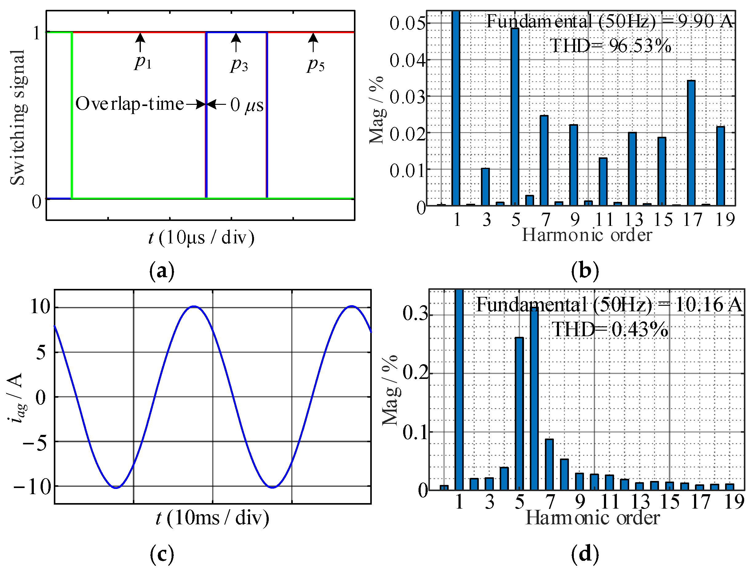
4.1. Harmonic Characteristics for Overlap Time

According to Table 1, the waveform of ∆ia is shown in Figure 8, the initial phase of ua is considered zero, and ∆ia can be expressed as
Δ i a = { 0 ( 0 ω t < π / 6 ) 2 i dc t d f s ( π / 6 ω t < 5 π / 6 ) 0 ( 5 π / 6 ω t < 7 π / 6 ) 2 i dc t d f s ( 7 π / 6 ω t < 11 π / 6 ) 0 ( 11 π / 6 ω t < 2 π ) .
This is the symmetry of half wave and quarter wave, so ∆ia only contains the odd-order harmonics, Equation (2) is decomposed into Fourier series, and the harmonic expression of ∆ia can be obtained as
Δ i a = 4 3 f s t ov i dc π { sin ω t + ( 1 ) k + 1 k = 1 [ 1 6 k 1 sin ( 6 k 1 ) ω t + 1 6 k + 1 sin ( 6 k + 1 ) ω t ] } .
Equation (3) shows that the overlap time introduces the 6k ± 1-order harmonics to the inverter-side current of CSI, and the amplitude of the harmonic is proportional to tov and idc.

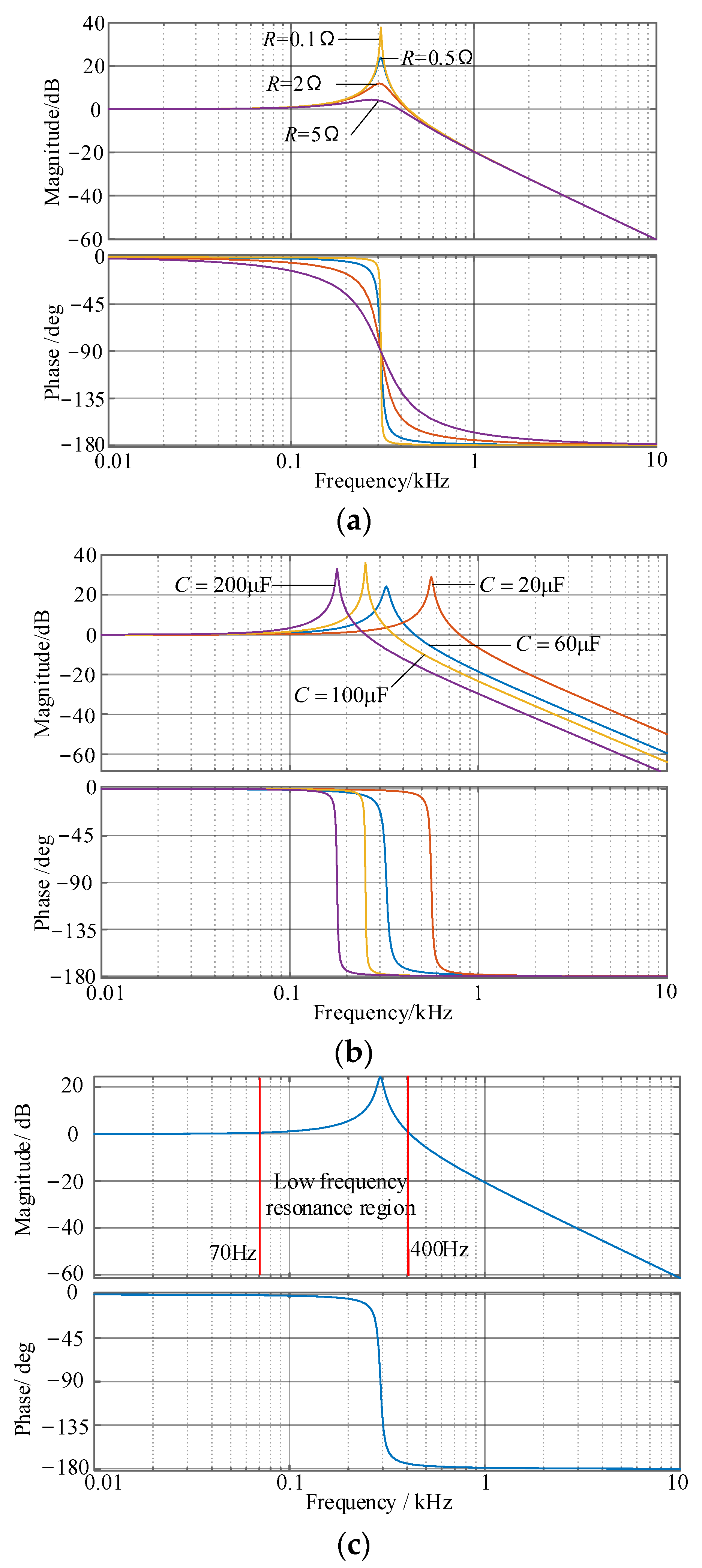
4.2. Parameters Design for L, C, and R

Next, the harmonics of the grid-side current caused by the overlap time will be discussed. According to Figure 1 and reference [29], the transfer function Gi2ig(s) from ia to iag can be derived as
G i 2 ig ( s ) = 1 L C s 2 + C R s + 1 .
The parameters of L, C, and R are determined by the Bode plots under different values. First, L and C remain unchanged. The Bode plots under different values of R are shown Figure 9a. The resonance peak decreases with the increase in R, but the efficiency of the system will decrease, so the value of R should be moderate. Meanwhile, the gain in the high-frequency range is independent of the value of R.
Then, L and R remain unchanged. The Bode plots under different values of C are shown Figure 9b. As the value of C increases, the high-frequency range gain increases, but the bandwidth of Gi2ig(s) decreases.
Since there are abundant high-order harmonics in the inverter-side current near the switching frequency, to achieve good filtering performance, this paper stipulates that the gain of Gi2ig(s) is less than 60 dB at the switching frequency of 10 kHz, so the values of L and C should be satisfied as
4 π 2 L C > 10 5 .
Based on the above analysis, the parameters of L, C, and R are set as 4 mH, 66 μF, and 0.5 Ω, respectively. Substituting these parameters into Equation (4), the Bode plot of Gi2ig(s) is shown in Figure 9c. To improve efficiency, the value of R is small, resulting in Gi2ig(s) being an under-damped system.
There is a resonance peak in the magnitude–frequency characteristic curve of Gi2ig(s), and Gi2ig(s) will amplify the harmonics whose frequency belongs to the range [70 Hz, 400 Hz] in the inverter-side current. According to the expression of the harmonic caused by the overlap time, the frequencies of the fifth and seventh harmonics are 250 Hz and 350 Hz, and belong to the resonance region, which shows that the overlap time will introduce fifth and seventh harmonic distortion to the gird-side current of CSI.

4.3. Analysis of Harmonic Losses Caused by Overlap Time

Since the fundamental component of the current and switching action times have no change, the conduction and switching losses have no relationship with the overlap time. However, the harmonic components in the inverter-side current generate harmonic losses on resistors. Taking the fifth harmonic as an example, according to Equations (3) and (4), the amplitude of fifth harmonic component in grid-side current can be derived as
I a g 5 = 4 3 f s t o v i d c 5 [ ω 5 2 C 2 R 2 + ( L C ω 5 2 1 ) 2 ] ,
where Iag5 is the amplitude of fifth harmonic component in iag, and ω5 is the angular frequency of the fifth harmonic, being equal to 500π rad/s. The whole harmonic loss Ph_loss caused by the overlap time is expressed as
P h _ l o s s = 72 f s 2 t o v 2 i d c 2 R 25 [ ω 5 2 C 2 R 2 + ( L C ω 5 2 1 ) 2 ] 2 .

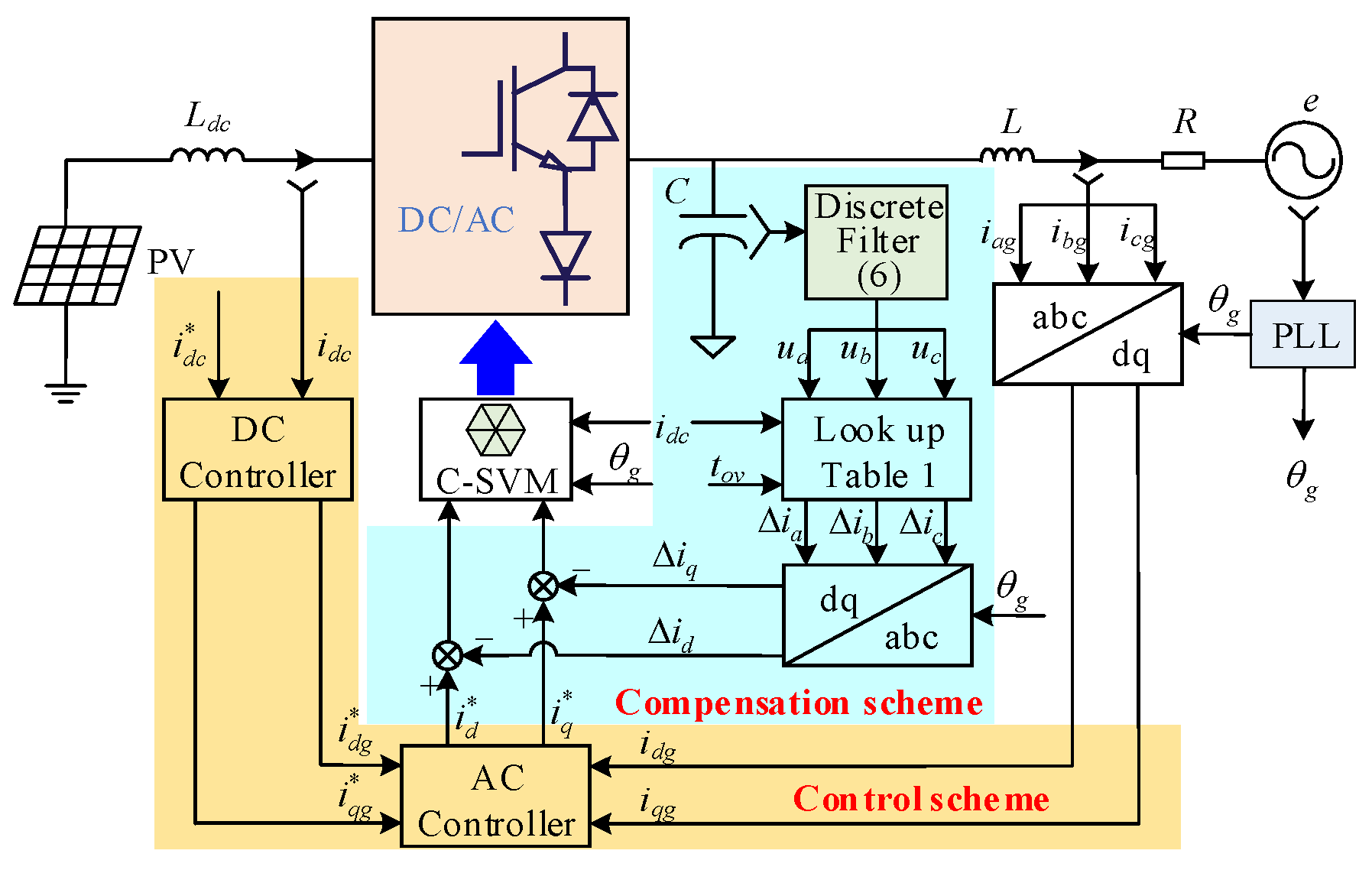
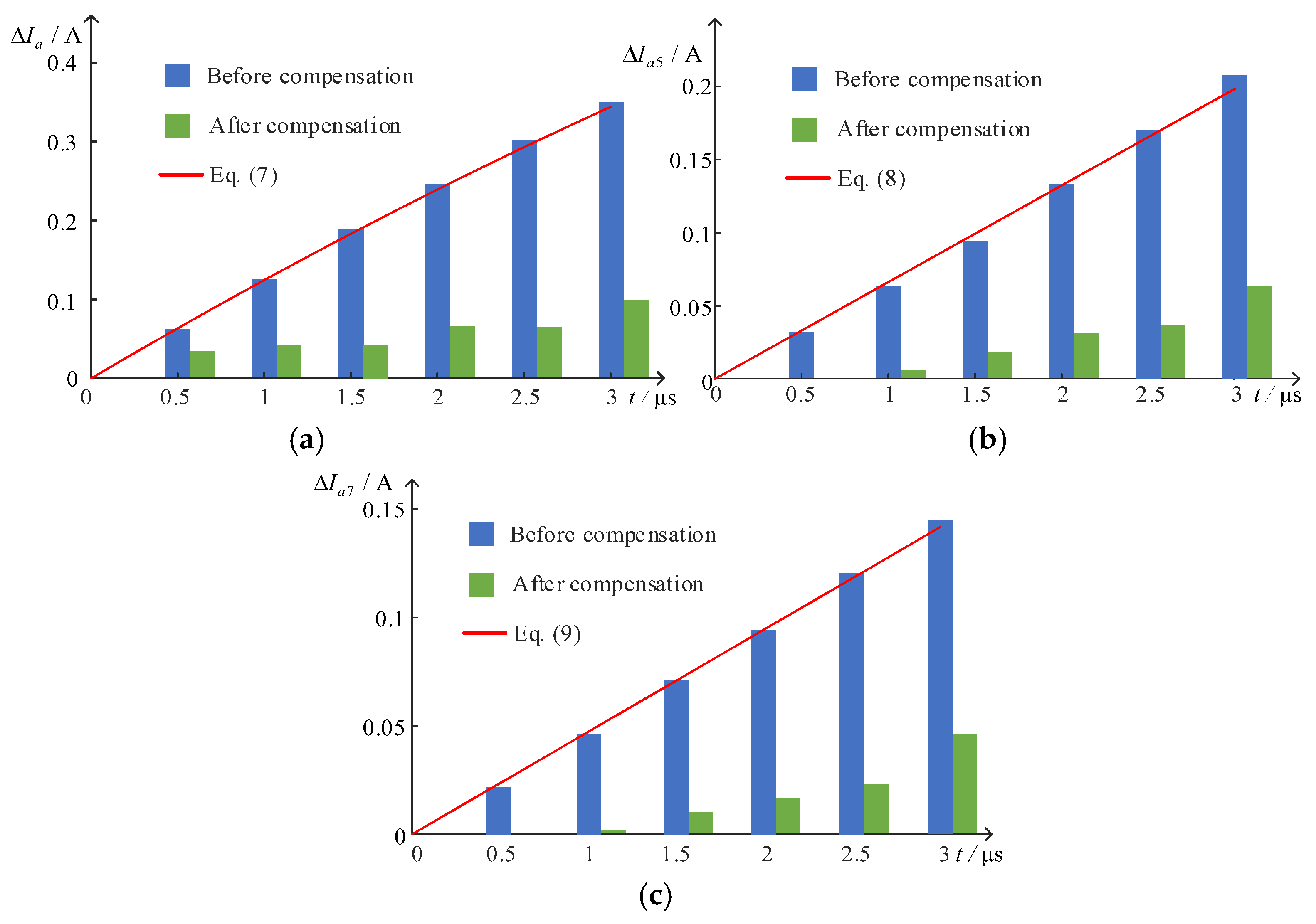
4.4. Compensation Scheme of the Overlap Time

Figure 10 shows the control structure of the current source PV grid-connected inverter. It contains the conventional double-loop control scheme and the proposed overlap time compensation, where θg represents the grid voltage angle and is detected by the phase-locked loop, idg and iqg represent the grid-side currents in d–q axis, and i dg * and i qg * represent the references of idg and iqg, respectively. i dc * is the reference of the DC-link current and is determined by the MPPT principle. The PI controller is adopted to regulate the DC-link current; its output is i dg * , and i qg * is commonly set to zero. idg and iqg are controlled by the PI controller with feedback decoupling and active damping, and the references of inverter-side currents in the d–q axis, i d * and i q * , are obtained.
Before implementing the SVPWM algorithm, compensation is required to eliminate the current error caused by the overlap time. First, the three-phase AC-side voltages are sampled at each carrier period, so ∆ia, ∆ib, and ∆ic can be obtained by looking up Table 1. Then, Clarke and Park’s transformations are performed, and the current errors of the inverter-side currents in the d–q axis, ∆id and ∆iq, are obtained. Before SVPWM, ∆id and ∆iq are subtracted from i d * and i q * , respectively.
According to Table 1, the proposed compensation scheme has a high requirement for AC voltage sampling accuracy. However, the filter capacitor absorbs the high-order harmonics of the inverter-side current, so there are significant ripples in the AC voltage, which seriously affect the sampling accuracy. If a low-pass filter is adopted, the phase delay will be generated, and the relations of the AC-side voltages will not be judged correctly. Therefore, a high-performance discrete filter is adopted to eliminate the ripple interference, its transfer function expression GR(z) in the z-domain is
G R ( z ) = 40 ω n T s ( 1 z 2 ) ω n 2 T s 2 + 40 ω n T s + 4 + 2 ( ω n 2 T s 2 4 ) z 1 ( 40 ω n T s ω n 2 T s 2 ) z 2 ,
where ωn is the fundamental angle frequency and Ts is the sampling period. The performance of GR(z) under Ts = 1 ms is shown in Figure 11. The fundamental wave of ua can be accurately extracted without phase shift under a low carrier ratio.

5. Simulation and Experimental Verification

5.1. Simulation Results and Analysis

In the environment of MATLAB 2022b/Simulink, the simulation models are established to verify the correctness of the analysis of the harmonic characteristics and the effectiveness of the proposed compensation method. The reference of the DC-link current is set as 15 A, fs is set as 10 kHz, the simulations are carried out under tov = 0 μs and tov = 3 μs, and the simulation waveforms and FFT results are shown in Figure 12 and Figure 13, respectively. Without the overlap time, it is obvious that there are very few harmonics in ia and iag. However, after the overlap time of 3 μs is introduced, the fundamental amplitude of ia, decreases from 9.90 A to 9.474 A, and the fifth harmonic, seventh harmonic, and total harmonic distortion (THD) significant increase. Affected by LC resonance, the harmonic distortion of iag is very significant; the ratios of the fifth harmonic and seventh harmonic are 4.52% and 3.56%.
To verify the correctness of the harmonic expression, the amplitude of the fundamental wave, fifth and seventh harmonics, and the THD of ia under different overlap times are simulated and shown in Table 2.
According to Equation (3), the fundamental of ia is expressed as
i a 1 = I a sin ( ω t φ ) 4 3 f s t ov i dc π sin ω t ,
where Ia is the fundamental amplitude of ia, φ is the phase of ia lagging ua, and is equal to 67°. In this operation, the amplitude loss of ia related to the overlap time can be derived as
Δ I a = I a ( I a sin φ ) 2 + ( I a cos φ 4 3 f s t ov i dc π ) 2 ,
where ∆Ia is the fundamental amplitude loss of ia. Since the contents of the fifth and seventh harmonics in ia are very few without the overlap time, ∆Ia5 and ∆Ia7, the amplitude increment of the fifth and seventh harmonics in ia, are approximately derived as
Δ I a 5 = 4 3 f s t ov i dc 5 π ,
Δ I a 7 = 4 3 f s t ov i dc 7 π
Under different overlap times, ∆Ia, ∆Ia5, and ∆Ia7, shown in Table 2, are compared with Equation (7) to Equation (9), respectively, and the comparison results are shown in Figure 13. The amplitude errors of the fundamental wave and fifth and seventh harmonics in ia are relatively close to the lines of Equations (7)–(9), which shows that the derived expression of the harmonic caused by the overlap time is theoretically correct.
Next, the proposed compensation model is introduced into the simulation, and the amplitude of the fundamental wave and fifth and seventh harmonics in ia are obtained and shown in Table 3. Meanwhile, comparison results with no compensation are reflected in Figure 14; the amplitude errors of the fundamental wave and fifth and seventh harmonics in ia, can be significantly reduced by the proposed compensation scheme. At this time, the simulation waveforms and FFT results of iag under tov = 3 μs are shown in Figure 15; compared to Figure 12 and Figure 13, the low harmonic distortion caused by the overlap time can be suppressed by the current error compensation.

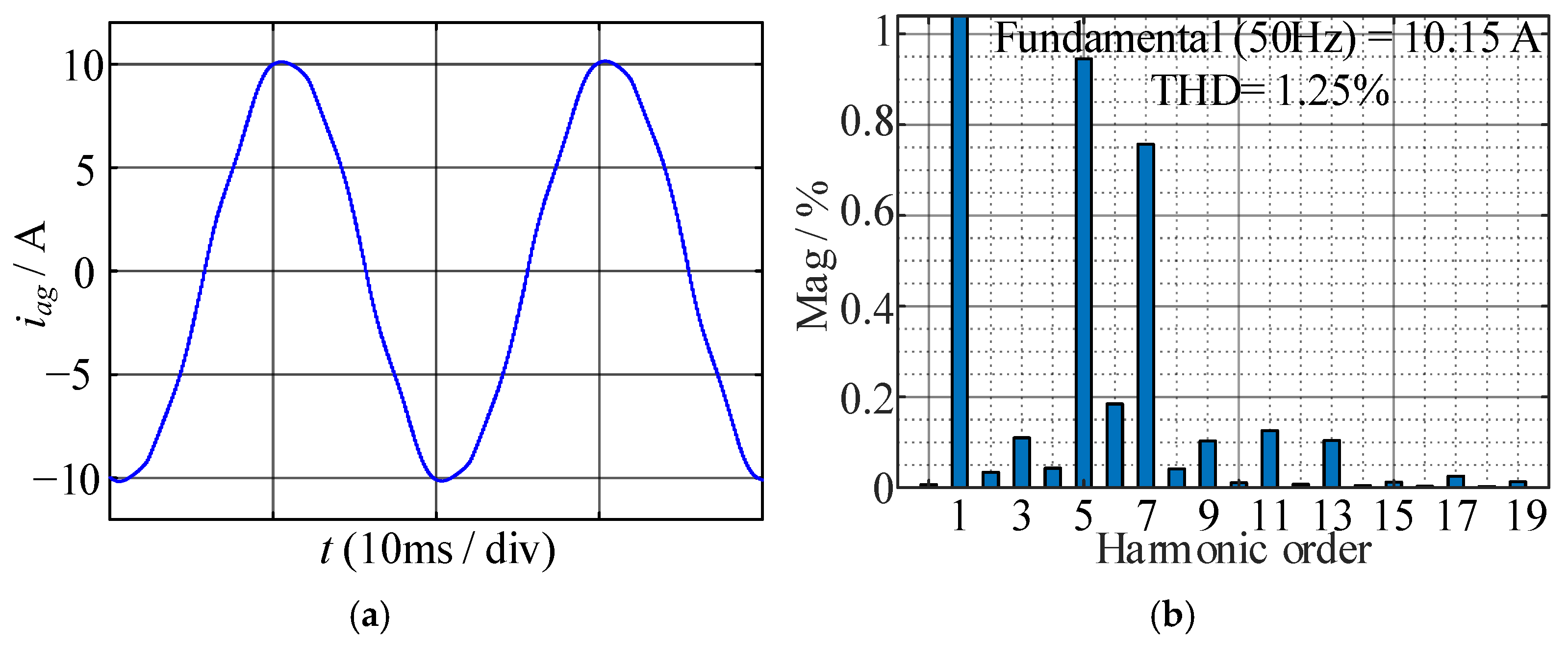
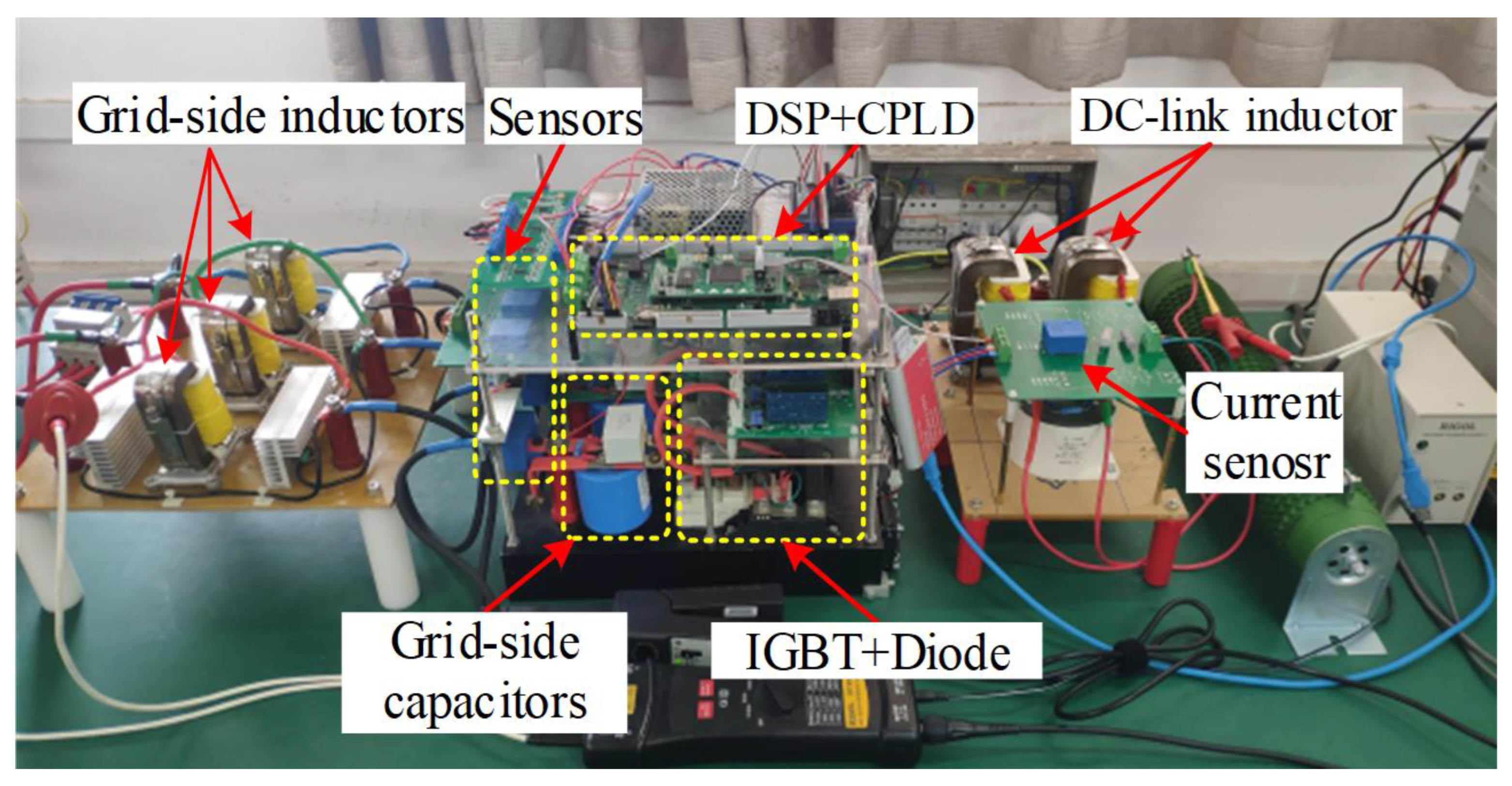
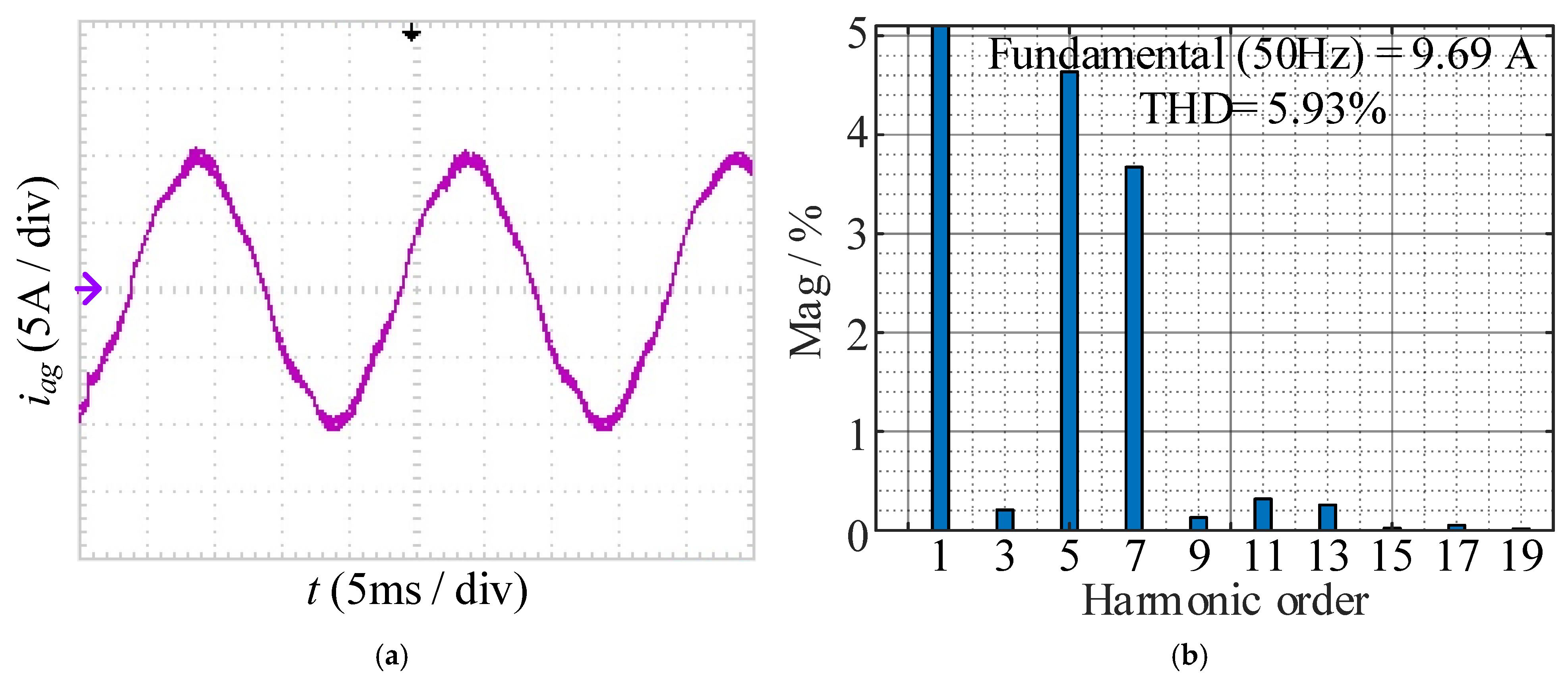
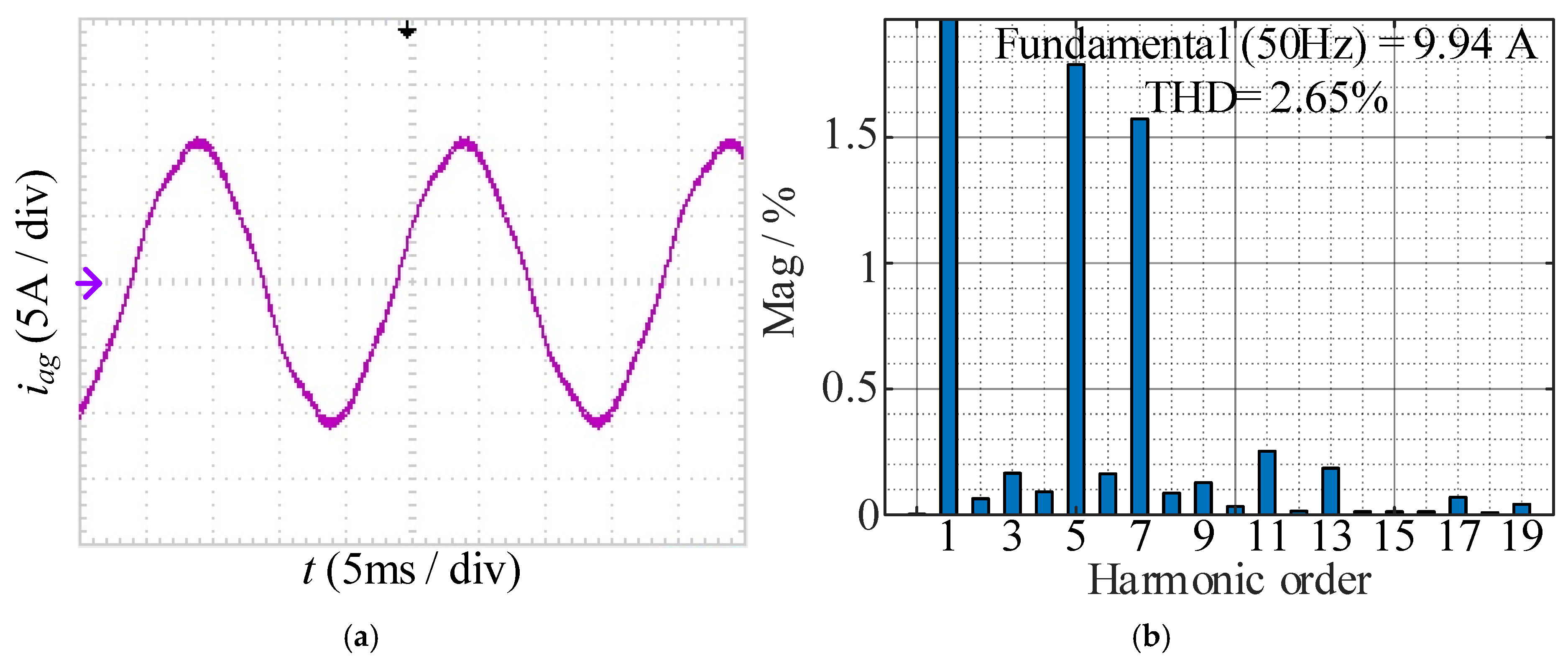
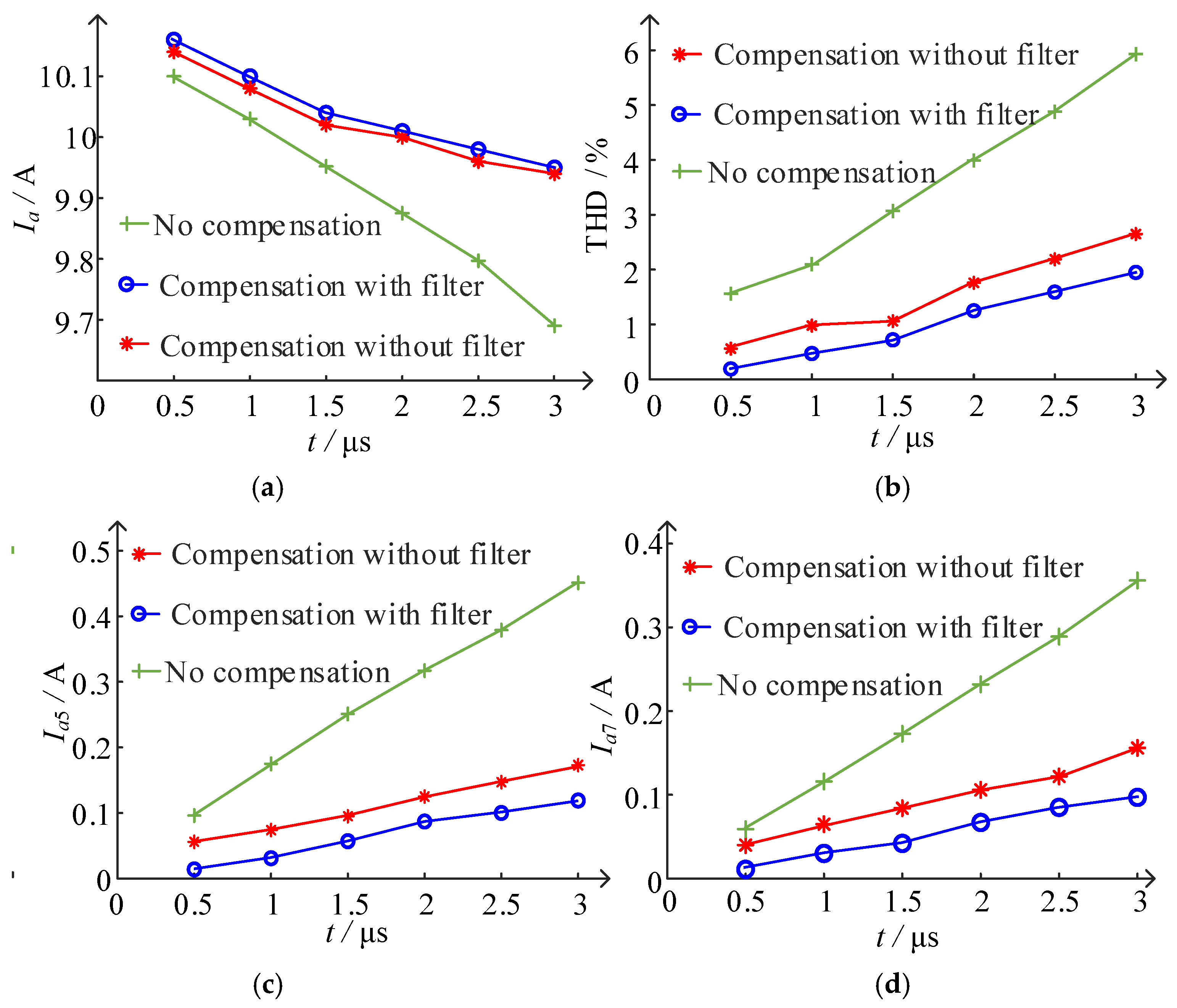
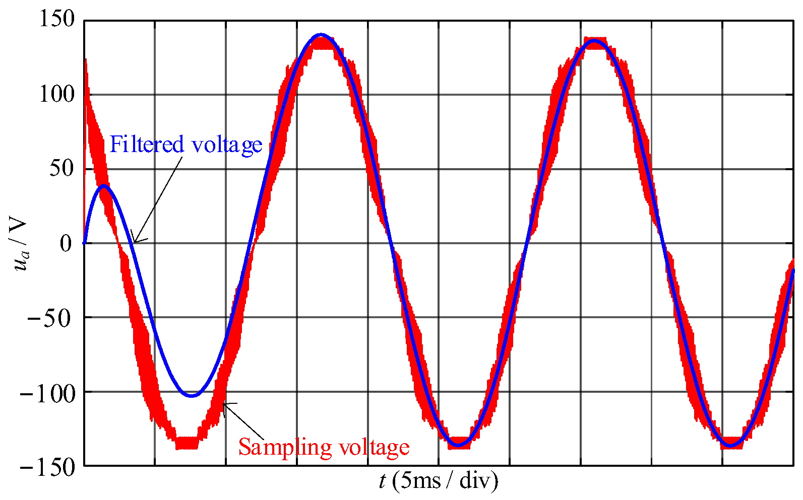
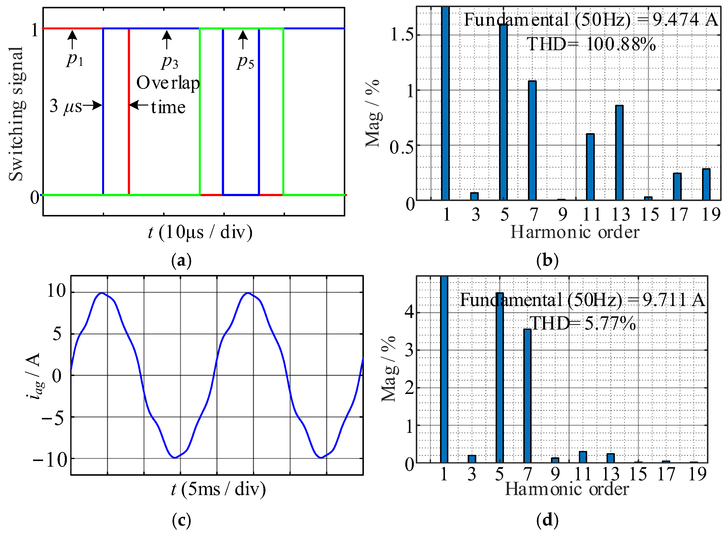
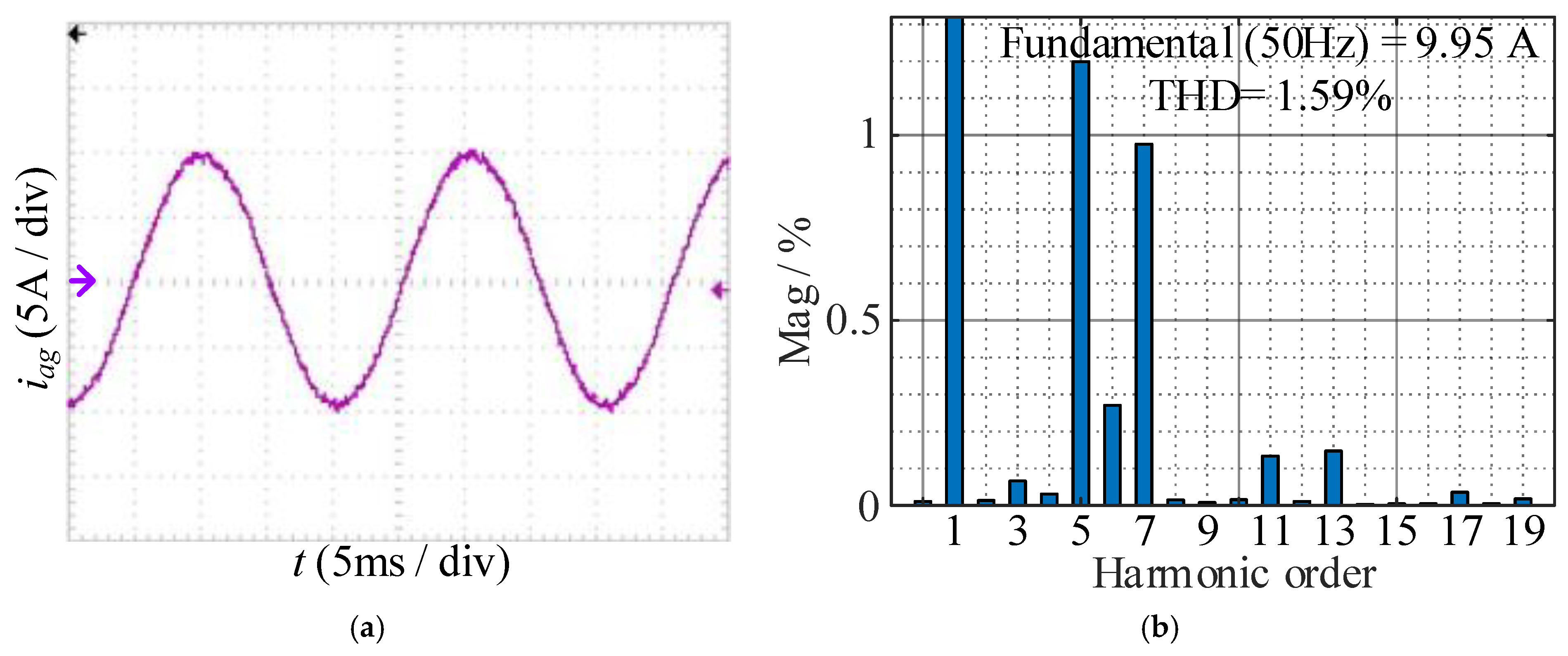
5.2. Experimental Results and Analysis

To further verify the effectiveness of the overlap time compensation method proposed in this paper, a prototype of the CSI is established and shown in Figure 16, and the part numbers and parameters of each component are listed in Table 4.
The operation of the experiment is the same as the simulation: idc = 15 A; fs = 10 kHz; tov = 3 μs. Without compensation, the experimental waveform and FFT result of iag are shown in Figure 17. Due to the overlap time effect and LC resonance, the obvious low-order harmonic distortion occurs in iag, where the amplitude of the fifth and seventh harmonics are 0.451 A and 0.356 A, respectively. It presents the same phenomenon as the simulation results shown in Figure 12.
After the proposed current error compensation is introduced into the control algorithm, the experimental waveform and FFT result of iag are shown in Figure 18; after compensation, the fundamental amplitude increase from 9.69 A to 9.95 A, the amplitudes of the fifth and seventh harmonics are reduced to 0.119 A and 0.097 A, and the THD decreases from 5.93% to 1.95%.
To demonstrate the necessity of the discrete filter Equation (9), Figure 19 shows the experimental waveform and FFT result of iag without a discrete filter. Due to the voltage sampling errors, the determination of the AC voltage relationships within a few carrier cycles is incorrect. Compared to Figure 18, although the fundamental amplitude can be compensated effectively, the suppression effect of the fifth and seventh harmonics is weaker than those adopted the discrete filter. The THD of iag is 2.65%, and the amplitudes of the fifth and seventh harmonics are 0.178 A and 0.158 A, respectively.
Figure 20 shows the comparison results of no compensation, compensation without discrete filter, and the proposed compensation under different overlap time, which shows that if the AC voltage relationship can be accurately obtained, the current error and harmonic distortion caused by the overlap time can be significantly compensated.

6. Conclusions

To prevent an open circuit fault in the current source inverter, the switching signal needs to be delayed and turned off, resulting in overlap time and low-order harmonics appearing in inverter-side and grid-side currents. In this paper, based on analyzing the nonlinear error and harmonic characteristics caused by the overlap time, a current compensation method with an AC voltage discrete filter is proposed. Finally, the correctness and effectiveness of the theoretical analysis and compensation scheme are certified via simulation and experiment, and our conclusions are formed as follows:
(1)
The current error during the overlap time is only determined by the relation of the AC-side voltage; it is not related to the sector of the target current vector.
(2)
The overlap time leads to a decrease in the fundamental wave and an increase in the low-order odd harmonics in the inverter-side current. Due to the LC resonance, the fifth and seventh harmonics in the grid-side current will further increase.
(3)
Since the AC-side voltage can be accurately obtained, the nonlinear errors caused by the overlap time can be significantly reduced by the proposed compensation scheme.
(4)
The proposed approach is dependent on the sampling accuracy of the filter capacitor voltage. Further research can focus on the control system bandwidth design and active damping method to suppress the harmonic distortion caused by the overlap time, eliminating the need for the sampling of the voltage.

Author Contributions

Conceptualization, C.X.; Methodology, Y.M.; Software, P.L.; Validation, P.L.; Investigation, Y.M.; Writing—original draft, Y.M.; Writing—review & editing, C.X.; Supervision, P.L.; Project administration, P.L.; Funding acquisition, C.X., P.L. and Y.M. All authors have read and agreed to the published version of the manuscript.

Funding

This work is supported by the grant of Ji Hua Laboratory (No. X220271XE220), and the natural sciences funding project of Fujian Province (No. 2022J01529 and No. 2022J05109).

Data Availability Statement

The data presented in this study are available on request from the corresponding author. The data are not publicly available due to the funder’s requirement.

Conflicts of Interest

The authors declare no conflict of interest.

References

  1. Dong, Z.; Wen, H.; Song, Z.; Liu, C. 3-D SVM for Three-Phase Open-End Winding Drives with Common DC Bus. IEEE Trans. Power Electron. 2023, 38, 9340–9346. [Google Scholar] [CrossRef]
  2. Song, P.; Liu, Y.; Liu, C. Research on Parameter Design and Control Method for Current Source Inverter–Fed IM Drive Systems. Machines 2022, 10, 922. [Google Scholar] [CrossRef]
  3. Liu, J.; Yang, M.; Tao, W. Impedance-Based Stability Analysis of Grid-Tied Photovoltaic System With Superconducting Magnetic Energy Storage System. IEEE Trans. Appl. Supercond. 2021, 31, 1–4. [Google Scholar] [CrossRef]
  4. Lin, Z.; Ruan, X.; Zhang, H.; Wu, L. A Generalized Real-Time Computation Method with Dual-Sampling Mode to Eliminate the Computation Delay in Digitally Controlled Inverters. IEEE Trans. Power Electron. 2021, 37, 5186–5195. [Google Scholar] [CrossRef]
  5. Freddy, T.K.S.; Rahim, N.A.; Hew, W.-P.; Che, H.S. Modulation techniques to reduce leakage current in three-phase transformerless H7 photovoltaic inverter. IEEE Trans. Ind. Electron. 2014, 62, 322–331. [Google Scholar] [CrossRef]
  6. Zhao, T.; Zhang, X.; Mao, W.; Wang, F.; Xu, J.; Gu, Y. A Modified Hybrid Modulation Strategy for Suppressing DC Voltage Fluctuation of Cascaded H-Bridge Photovoltaic Inverter. IEEE Trans. Ind. Electron. 2017, 65, 3932–3941. [Google Scholar] [CrossRef]
  7. Xing, L.; Wei, Q. Series-Connected Current Source Inverters with Less Switches. IEEE Trans. Power Electron. 2019, 35, 5553–5556. [Google Scholar] [CrossRef]
  8. Wang, W.; Gao, F.; Yang, Y.; Blaabjerg, F. An Eight-Switch Five-Level Current Source Inverter. IEEE Trans. Power Electron. 2019, 34, 8389–8404. [Google Scholar] [CrossRef]
  9. He, J.; Li, Q.; Zhang, C.; Han, J.; Wang, C. Quasi-Selective Harmonic Elimination (Q-SHE) Modulation-Based DC Current Balancing Method for Parallel Current Source Converters. IEEE Trans. Power Electron. 2018, 34, 7422–7436. [Google Scholar] [CrossRef]
  10. Rajeev, M.; Agarwal, V. Single Phase Current Source Inverter With Multiloop Control for Transformerless Grid–PV Interface. IEEE Trans. Ind. Appl. 2018, 54, 2416–2424. [Google Scholar] [CrossRef]
  11. Chen, D.; Jiang, J.; Qiu, Y.; Zhang, J.; Huang, F. Single-Stage Three-Phase Current-Source Photovoltaic Grid-Connected Inverter High Voltage Transmission Ratio. IEEE Trans. Power Electron. 2016, 32, 7591–7601. [Google Scholar] [CrossRef]
  12. Azghandi, M.A.; Barakati, S.M.S.; Yazdani, A. Impedance-Based Stability Analysis and Design of a Fractional-Order Active Damper for Grid-Connected Current-Source Inverters. IEEE Trans. Sustain. Energy 2020, 12, 599–611. [Google Scholar] [CrossRef]
  13. Miao, Y.; Liao, W.; Huang, S.; Liu, P.; Wu, X.; Song, P.; Li, G. DC-Link Current Minimization Scheme for IM Drive System Fed by Bidirectional DC Chopper-Based CSI. IEEE Trans. Transp. Electrif. 2022, 9, 2839–2850. [Google Scholar] [CrossRef]
  14. Guo, X.-Q.; Sui, S.; Wang, B.; Zhang, W. A Current-Based Approach for Short-Circuit Fault Diagnosis in Closed-Loop Current Source Inverter. IEEE Trans. Ind. Electron. 2019, 67, 7941–7950. [Google Scholar] [CrossRef]
  15. Guo, X.; Du, S.; Diao, N.; Hua, C.; Blaabjerg, F. Three-Dimensional Space Vector Modulation for Four-Leg Current-Source Inverters. IEEE Trans. Power Electron. 2023, 38, 13122–13132. [Google Scholar] [CrossRef]
  16. Zhang, Y.; Yang, T.; Miao, Y. Research on the Modulation and Control Strategy for a Novel Single-Phase Current Source Inverter. Energies 2023, 16, 6729. [Google Scholar] [CrossRef]
  17. Barakat, M. Novel chaos game optimization tuned-fractional-order PID fractional-order PI controller for load–frequency control of interconnected power systems. Prot. Control Mod. Power Syst. 2022, 7, 1–20. [Google Scholar] [CrossRef]
  18. Chierchie, F.; Paolini, E.E.; Stefanazzi, L. Dead-Time Distortion Shaping. IEEE Trans. Power Electron. 2019, 34, 53–63. [Google Scholar] [CrossRef]
  19. Ding, L.; Li, Y.W.; Zargari, N.R. Discrete-time SMO sensorless control of current source converter-fed PMSM drives with low switching frequency. IEEE Trans. Ind. Electron. 2020, 68, 2120–2129. [Google Scholar] [CrossRef]
  20. Hwang, S.-H.; Kim, J.-M. Dead Time Compensation Method for Voltage-Fed PWM Inverter. IEEE Trans. Energy Convers. 2010, 25, 1–10. [Google Scholar] [CrossRef]
  21. Lee, J.-H.; Sul, S.-K. Inverter Nonlinearity Compensation Through Deadtime Effect Estimation. IEEE Trans. Power Electron. 2021, 36, 10684–10694. [Google Scholar] [CrossRef]
  22. Wang, W.; Gao, F.; Yang, Y.; Blaabjerg, F. Operation and modulation of H7 current-source inverter with hybrid SiC and Si semiconductor switches. IEEE J. Emerg. Sel. Top. Power Electron. 2017, 6, 387–399. [Google Scholar] [CrossRef]
  23. Gaber, M.; Abdel-Rahim, O.M.; Orabi, M. Novel Overlap Method to Eliminate Vector Deviation Error in SVM of Current Source Inverters. IEEE Trans. Power Electron. 2020, 36, 2320–2333. [Google Scholar] [CrossRef]
  24. Guo, B.; Xu, F.; Zhang, Z.; Xu, Z.; Wang, F.; Tolbert, L.M.; Blalock, B.J. Compensation of Input Current Distortion in Three-phase Buck Rectifiers. In Proceedings of the 2013 Twenty-Eighth Annual IEEE Applied Power Electronics Conference and Exposition (APEC), Long Beach, CA, USA, 17–21 March 2013; pp. 930–938. [Google Scholar]
  25. Qin, H.; Zhang, X.; Zhu, Z.; Ma, C.; Xu, H. Influence of overlap-time on the ac grid-side current of current source PWM rectifier and restraining method. Trans. China Electrotech. Soc. 2016, 31, 142–152. [Google Scholar]
  26. Geng, Y.; Deng, R.; Dong, W.; Wang, K.; Liu, H.; Wu, X. An Overlap-Time Compensation Method for Current-Source Space-Vector PWM Inverters. IEEE Trans. Power Electron. 2017, 33, 3192–3203. [Google Scholar] [CrossRef]
  27. Guo, X. A Novel CH5 Inverter for Single-Phase Transformerless Photovoltaic System Applications. IEEE Trans. Circuits Syst. II Express Briefs 2017, 64, 1197–1201. [Google Scholar] [CrossRef]
  28. Guo, Q.; Liu, H.; Peng, D.; Liu, Q. A Current-Source Charging System Considering the Characteristics of Battery. Trans. China Electrotech. Soc. 2016, 31, 16–25. [Google Scholar]
  29. Guo, Q.; Zhou, C.; Li, S. A Multiple Loops Control Strategy Based on DC Link Voltage of Current Source PWM Rectifiers. Trans. China Electrotech. Soc. 2022, 37, 2051–2063. [Google Scholar]
Figure 1. Topology of the current source PV grid-connected inverter.
Energies 17 01768 g001
Figure 2. Current vectors and sectors.
Energies 17 01768 g002
Figure 3. Switching signals diagrams in a carrier period under seven-segment SVM: (a) sector I; (b) sector II.
Energies 17 01768 g003
Figure 4. Switching signals diagrams with overlap time.
Energies 17 01768 g004
Figure 5. Equivalent circuit during the overlap time: (a) commutation from I7 to I1; (b) commutation from I8 to I1.
Energies 17 01768 g005
Figure 6. The diagrams of ia, ib, and ic with their error caused by the overlap time in sector I: (a) ua > ub > uc; (b) ua > uc > ub; (c) ub > ua > uc; (d) ub > uc > ua; (e) uc > ua > ub; (f) uc > ub > ua.
Energies 17 01768 g006
Figure 7. The diagrams of ia, ib, and ic with their error caused by the overlap time in sector II: (a) ua > ub > uc; (b) ua > uc > ub; (c) ub > ua > uc; (d) ub > uc > ua; (e) uc > ua > ub; (f) uc > ub > ua.
Energies 17 01768 g007
Figure 8. Waveform of ∆ia.
Energies 17 01768 g008
Figure 9. Bode plot of Gi2ig(s): (a) different R; (b) different C; (c) parameters determined in this paper.
Energies 17 01768 g009
Figure 10. Control structure with compensation of the overlap time.
Energies 17 01768 g010
Figure 11. The waveforms of ua before and after the discrete filter.
Energies 17 01768 g011
Figure 12. Simulation results without overlap time: (a) switching signals; (b) FFT results of ia; (c) iag, (d) FFT results of iag.
Energies 17 01768 g012
Figure 13. Simulation results with overlap time of 3 μs: (a) switching signals; (b) FFT results of ia; (c) iag; (d) FFT results of iag.
Energies 17 01768 g013
Figure 14. Comparison results of no compensation, proposed compensation, and derived harmonic expressions: (a) ∆Ia; (b) ∆Ia5; (c) ∆Ia7.
Energies 17 01768 g014
Figure 15. Simulation results after compensation under tov = 3 μs: (a) waveform of iag; (b) FFT results of iag.
Energies 17 01768 g015
Figure 16. Experimental prototype of CSI.
Energies 17 01768 g016
Figure 17. Experimental results without compensation under tov = 3 μs: (a) waveform of iag; (b) FFT result of iag. Purple arrow—the zero tick mark.
Energies 17 01768 g017
Figure 18. Experimental results with compensation under tov = 3 μs: (a) waveform of iag; (b) FFT result of iag. Purple arrow—the zero tick mark.
Energies 17 01768 g018
Figure 19. Experimental results with compensation and no discrete filter under tov = 3 μs.: (a) waveform of iag; (b) FFT results of iag. Purple arrow—the zero tick mark.
Energies 17 01768 g019
Figure 20. The comparison results of no compensation, compensation without discrete filter, and the proposed compensation under different overlap time: (a) fundamental amplitude; (b) THD; (c) amplitude of fifth harmonic; (d) amplitude of seventh harmonic.
Energies 17 01768 g020
Table 1. Average current error caused by the overlap time.
Relation of AC Voltageiaibic
ua > ub > uc−2fstovidc02fstovidc
ua > uc > ub−2fstovidc2fstovidc0
ub > ua > uc0−2fstovidc2fstovidc
ub > uc > ua2fstovidc−2fstovidc0
uc > ua > ub02fstovidc−2fstovidc
uc > ub > ua2fstovidc0−2fstovidc
Table 2. Average current error caused by the overlap time.
Overlap-
Time (μs)
Fundamental Amplitude(A)Fifth Harmonic Amplitude (A)Seventh Harmonic Amplitude (A)THD
(%)
09.900.0050.00396.53
0.59.8350.0370.02597.20
19.7760.0690.04997.89
1.59.7130.0980.07498.61
29.6560.1400.09799.35
2.59.5920.1750.122100.09
39.5430.2130.148100.88
Table 3. The low harmonic characteristics of ia after the proposed compensation.
Overlap-
Time (μs)
Fundamental Amplitude(A)Fifth Harmonic Amplitude (A)Seventh Harmonic Amplitude (A)THD
(%)
0.59.8970.0050.00396.55
19.8960.0090.00596.56
1.59.8960.0170.00996.57
29.8900.0280.01896.57
2.59.8900.0410.02796.57
39.8760.0680.04996.65
0.59.8970.0050.00396.55
Table 4. The part numbers and parameters of each component.
CategoryPart NumberParameter
AC voltage simulatorChroma 61830100 V
DC input voltageDS102050 V
ControllerTMS320F28335 + CPLD/
Voltage sensorLV28-P/
Current sensorLA200-p/
Switching tubeFF100R12RT4/
DiodeMEA75-12DA/
DC-link inductance/8 mH
AC-side inductance/4 mH
AC-side capacitance/66 µF
AC-side resistance/0.5 Ω
Disclaimer/Publisher’s Note: The statements, opinions and data contained in all publications are solely those of the individual author(s) and contributor(s) and not of MDPI and/or the editor(s). MDPI and/or the editor(s) disclaim responsibility for any injury to people or property resulting from any ideas, methods, instructions or products referred to in the content.

