Article

Analysis, Design and Effectuation of a Tapped Inductor Current Converter with Fractional Output for Current Source Systems

Power Electronics Research Center, The Hong Kong Polytechnic University, Hong Kong 999077, China
*
Author to whom correspondence should be addressed.
Energies 2024, 17(9), 2204; https://doi.org/10.3390/en17092204
Submission received: 10 December 2023 / Revised: 13 April 2024 / Accepted: 30 April 2024 / Published: 3 May 2024
(This article belongs to the Section F3: Power Electronics)

Abstract

:
This article proposes a new connection method of tapped inductors that works in the current source, which enables the current-mode power converter circuit to have a new topological relationship. Usually, in a switched-inductor circuit, a stable output multiple is obtained through the connection of the inductor and the switching devices. This is because the tapped point on the inductor varies, and the magnetomotive force (mmf) of inductance is adjusted. Thereby, the output current is controlled by the states of switching devices within a certain range. This optimized circuit structure can adjust the output current according to load changes in practical applications without changing the input power supply. The proposed method has been verified for its feasibility through detailed analysis and hardware work. The principal analysis based on the flux linkage and the PSIM simulation confirms that the theoretical circuit can be implemented. Finally, a hardware circuit is built to obtain real and feasible conclusions, and it is verified that the circuit can achieve a stable output and variable current within a specific range. The proposed work presents an alternative power conversion methodology using the active switching of mmf, and it is a stable and simple power conversion technique.

1. Introduction

1.1. Backgrounds

The power converter is widely used in automotive electronic equipment, communication systems, industrial automation, and new energy systems [1]. However, most current application conversions are based on voltage mode usage scenarios [1,2,3,4]. The current source converters mentioned in this article are usually buried inside the electronic circuit and are not easy to see; the internal resistance of an ideal current source is infinite. When it supplies power to the load circuit, the current source can maintain a constant current output and adjust the voltage [5]. Current mode source power supply systems are mainly used in some professional fields. For example, the electric energy generated by the solar panel [6,7] is directly proportional to the intensity of illumination on the solar panel. The current increases when the light intensity increases, and when the sunlight weakens or disappears, the current decreases. For the operation of a light-emitting diode (LED) power supply system [8], if the LED brightness is stable, the chromaticity is consistent, and the service life is improved, it is necessary for control to continue to work under a constant current. This type of circuit requires a current mode source to supply power. In addition, current sources also apply the conversion of Wireless Power Transmission (WPT) [9] and the charging of high-power energy storage systems of electric vehicles [1,10,11,12,13,14,15,16].
Generally, the output current of a current source converter needs to be kept stable [17]. Otherwise, it can lead to a decrease in power distribution efficiency or damage to the load equipment [18]. If a small part or parasitic of the circuit structure is changed, the output current of the current source can be changed within a specific range and maintain a stable output, and the current source can be applied to more application scenarios. For example, in quick charging, the current of a high-power energy storage system needs to be large first and then reduced to small [9]; doubling the current of the wireless charging receiving end through a multi-stage circuit can reduce the current’s requirement by the electromagnetic coil, thereby reducing energy loss. In addition, inductors can also be used as energy storage components. Compared with capacitor energy storage, inductors have better performance under long-term continuous working conditions. Also, an inductive output configuration enables a stable and constant output current.
The circuit studied in this article adds a tapped inductor [4,17,19,20,21] to the course. This connection method can change the inductance at both ends of the inductor by moving the position of the point of the tap on the inductor. In a high-frequency working environment [22], and under different working steps, the inductance can be changed and supply a different current. The inductance at both ends brings different output results, which gives the current power converter circuit a new topological relationship. In this working mode, the incoming current source can change the output current within a specific range to adapt to multiple relationships. Thus, it is applied to a variety of electrical equipment. In addition, the current’s increase in the circuit causes the core material to be saturated and more energy loss, thus causing changes in inductance. This requires special attention during research. When selecting the required tap inductor, it is necessary to reserve a sufficient current margin and temperature rise in space to ensure the stability of the output current of the entire circuit [23,24,25].
In this paper, based on theoretical analysis, the inductor replaces the capacitor and is connected in a specific way to obtain a new circuitry. The circuit is converted to a current mode. The proposed new circuit can be examined for its principle of operation, and it can be applied to the current source and current sink application. Then, the theoretical circuit is simulated through p-sim to obtain results in order to verify the theoretical analysis. Finally, the experiment is carried out by designing a hardware circuit with a variable DC current-mode converter with the output of 1 to 2 times with the input. The voltage and current changes at each critical point in the circuit are examined. The results verified that the circuit could achieve a stable output of variable current within a certain range.
Through this experiment, we can discern the topology of the current mode and tapped inductor circuits and theory correlations. For different application scenarios, we can use DC converters with different conversion ratios and achieve better output efficiency and current conversion requirements.

1.2. Basic Concept of the Duality

The starting point of the present research is based on the switched-capacitor converter [23] and the duality principle in the circuit theory. Figure 1 shows a conventional switched-capacitor converter, which is a double mode, i.e., Vo/Vin = 2. Table 1 and Figure 2 are the translation methods between the voltage mode and current mode using the duality principle [3]. The translational is directional, i.e., if it is originally a star connection, it is translated to a delta connection.

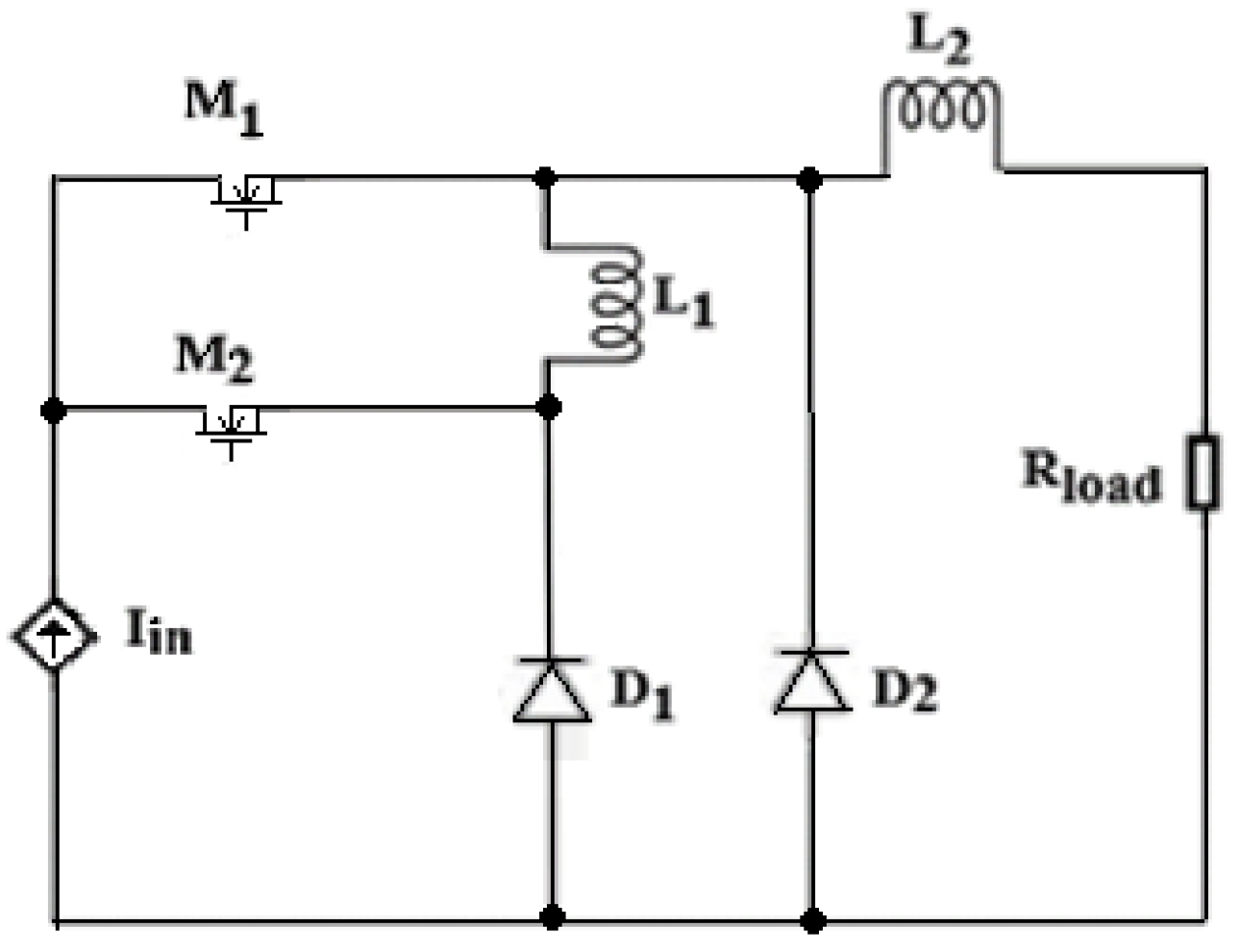
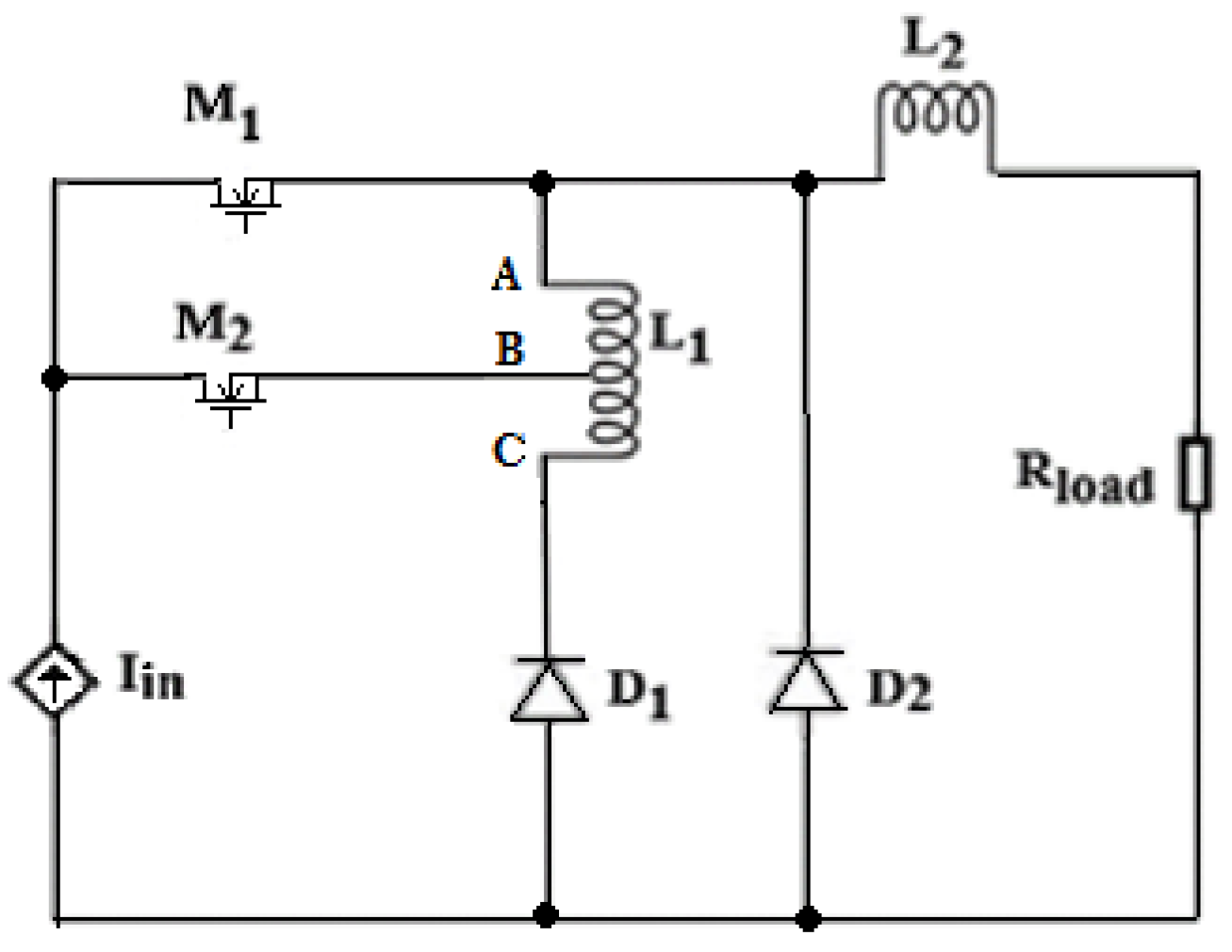
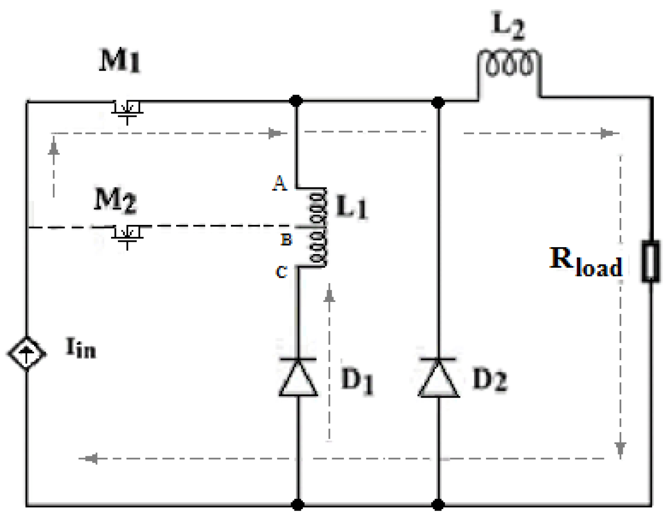
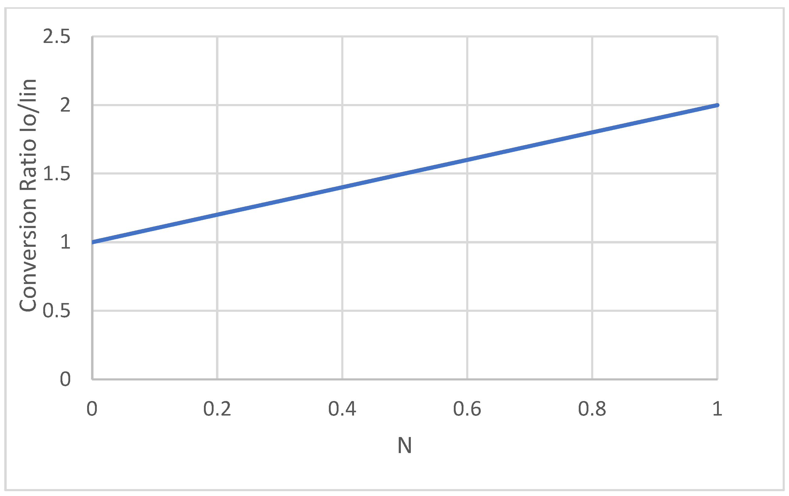
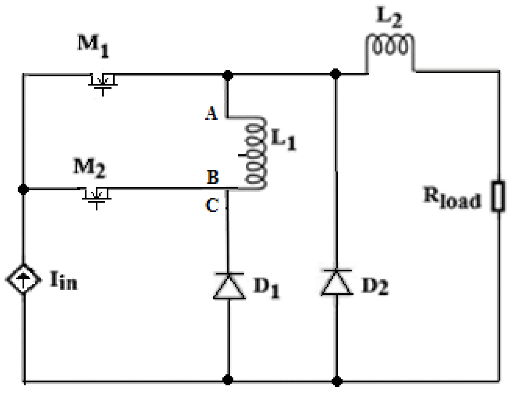
2. Tapped Inductor Converter Circuit Analysis

Based on the double mode current type switch inductor converter circuit [2,3] shown in Figure 3, when one MOSFET source pin is tapped to the middle of the inductor, the tapped point can be moved to either side of the inductor. When the tapped point moves from A to C, the output current increases. The new circuit can be seen in Figure 4.
With this circuit input, the current is 4 A, and MOSFET 1 (M1) and MOSFET 2 (M2)’s operating frequency is 100 kHz; they conduct in a complementary manner, and each of them works under the duty cycle of 50%. The resistance for the load is 2 Ω. The inductors L1 and L2 are all 100 μH. The circuit has two stages of operation and is continuous. During the first stage, the input current can flow through M1; there is no current flow from M2 to L1, and the direction of the current flow can be seen in the figure. The current flowing through output resistance is the input current, adding the current maintained in L1 due to the flux linkage coupled between parts B and C.
Stage 1 shows the current flow equivalent circuit that can be seen in Figure 5, and Stage 2’s circuit current flow can be seen in Figure 6.
Stage 1: The principal equations are as follows:
I M 1 = I i n
I o u t = I L 2 = I i n + I L 1
For Stage 2, the key equations are as follows:
I M 2 = I i n = I L 1 A B
I o u t = I i n + I D 2
According to Faraday’s law of electromagnetic induction, an induced electromotive force is generated in a coil when the magnetic flux varies with time, and the magnetomotive force (mmf) is equal to the ampere-turns that remain the same during the first and second stages.
m m f = N I
N is the number of turns of the coil; I is the respective current of the turns. So,
I L 1 A B N 1 A B = I L 1 · N 1
I L 1 = N 1 A B N 1 I L 1 A B
L1AB is tapped from L1, and is part of L1. We set L1AB = N2L1, where 0 N 1 . The turns ratio is simply an inverted current ratio.
I L 1 = N · I i n
I o u t = I i n   + I L 1   = ( 1 + N ) · I i n
I o u t I i n = 1 + N
So, the output current is 1 to 2 times the input current. Figure 7 shows the output current conversion ratio. The output current value depends on the coil current IL1AB and the actual inductance current IL1AB.

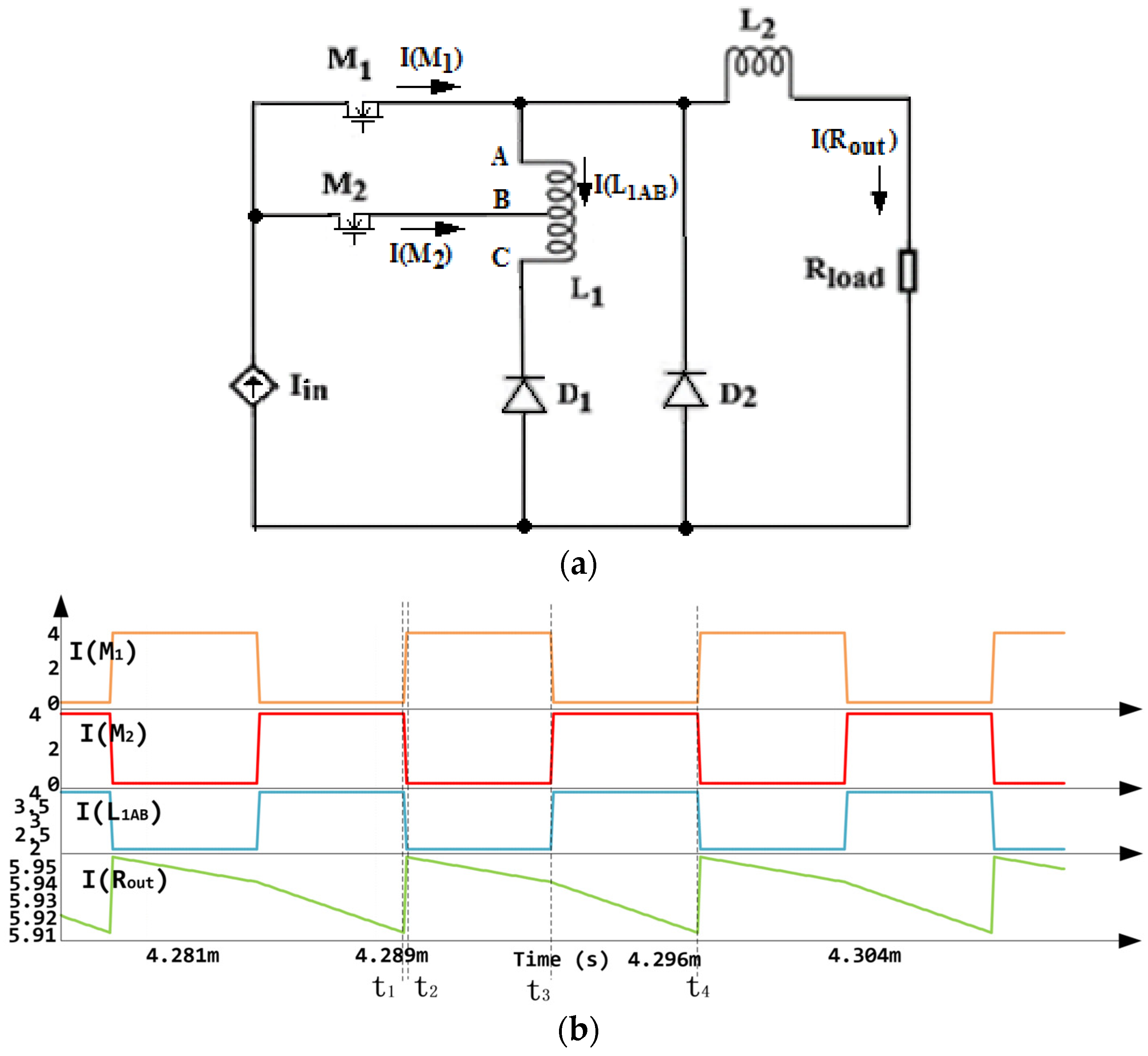
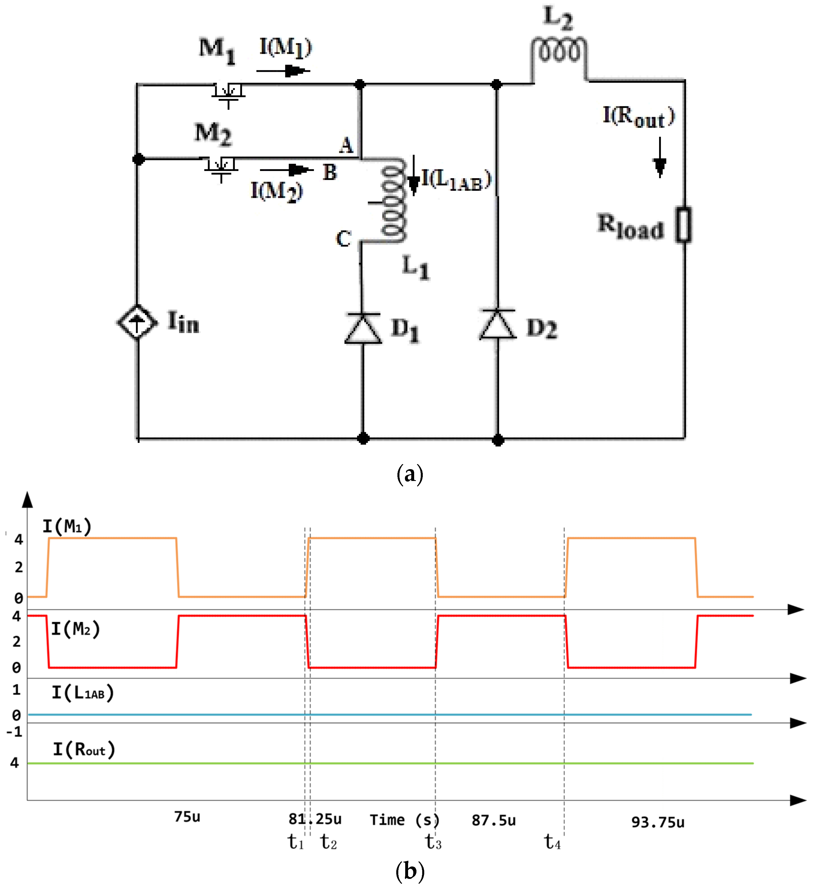
3. Tapped Inductor Converter Work on P-SIM Results
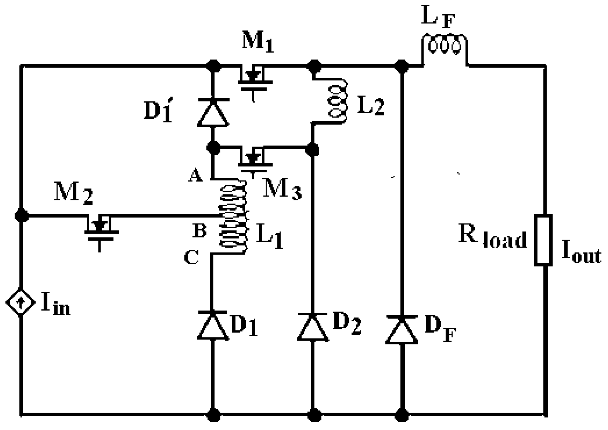
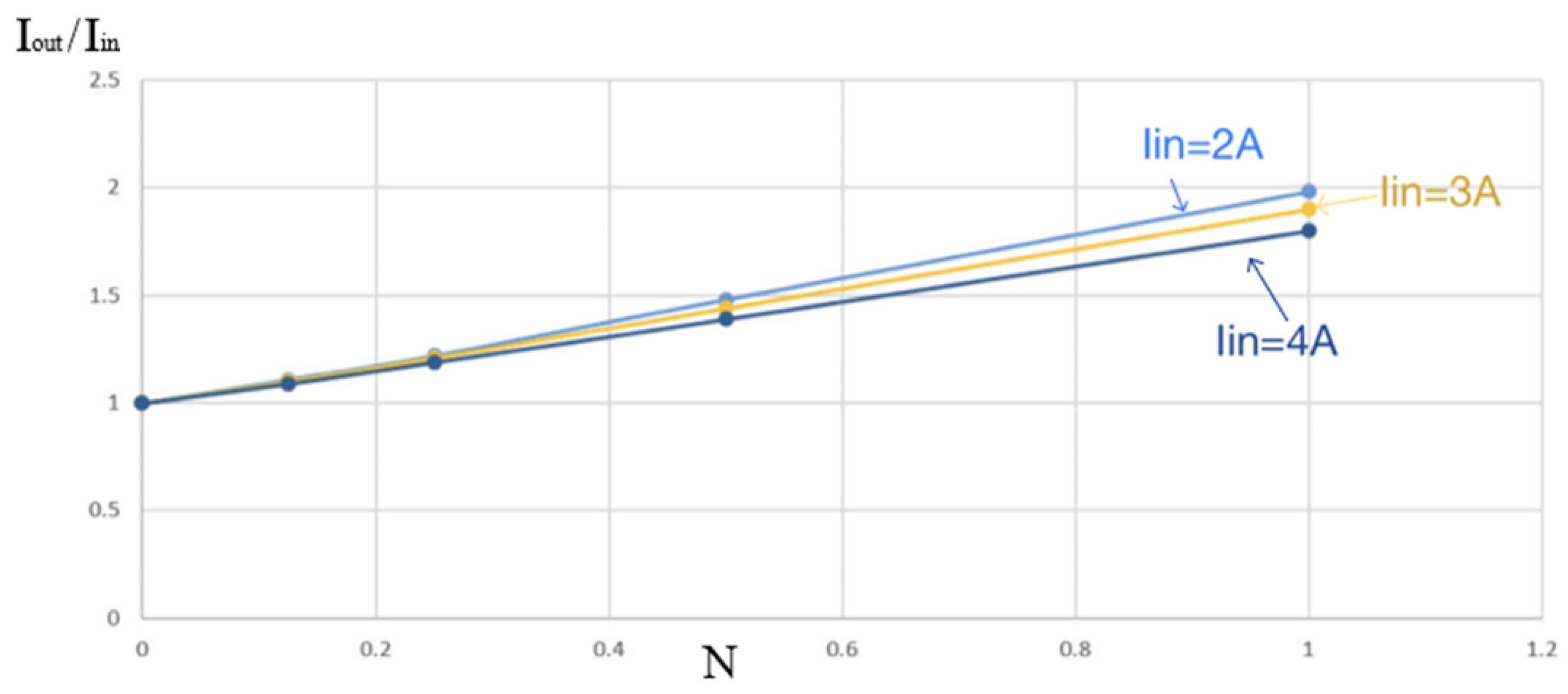
This part of the software testing uses psim2022 for the student-free version; in the simulation, the input current is 4 A, the inductance values of L1 and L2 are all 1 mH, and the output load is 1 Ω. A and C are either terminals of L1 and B is the connection tap point from M2’s source.
When the inductor L1’s A point connects to the M1’s source, B is moved to the same connection point as C, which is the same point as the M2 source and D1 cathode. The equivalent circuit is shown in Figure 8. At this part, when M2 is conducting, the current flow through the inductor L1 is via M2.
The currents through each component are simulated, as shown in Figure 9. Stage 1 is the time from t1 to t3. At this stage, M1 is switched on, and M2 is switched off; it can be seen that the current flow at M1 increases from 0 A to 4 A, the current flow at M2 drops from 4 A to 0 A, and the current flow at L1 drops from 4 A to 3.92 A, which means that the power in L1 is used for the load. This also verifies that, in this stage, the load current is provided by the input power supply and L1 together. There is conduction overlapping between M1 and M2 as this is the current mode, and the deadline is negative. Negative dead time is a switching feature in the current mode because the current in the inductor or the current source cannot be interrupted and must be conducted by any one of the switching devices. The current flow through the resistance load rises to 7.94 A [t1t2]. As L1 is finite, the current drops slightly [t2t3]. Stage 2 is the time from t3 to t4. At this stage, M1 is switched off, and M2 is switched on; the current in M1 drops from 4 A to 0 A. The source current then flows through M2, and its current rises from 0 A to 4 A; the current is the same as that through L1, in which the current flow through the resistance load dropped fast to 7.88 A [t3t4]. From the test data, the simulation result of the output RMS current is 7.92 A, which is close to two times the input current. This is because of the loss in the components, which usually makes the conversion slightly lower.
Using the same test method as before, when the tapped point B is in the middle point (center tap) of the inductor, the test circuit and simulation waveform are shown in Figure 10, and the output RMS current is 5.94 A, which is about 1.5 times the input current.
When inductor L1’s A and B points connect to the M1 source and M2 source, respectively, and become a common potential. C connects with the D1 cathode; the performance of the circuit is illustrated using a simulation and is shown in Figure 11. In this test, when M2 conducts, the current cannot flow through the inductor L1. The sum of currents flowing through M1 and M2 is the same as I(Rout). D1 has no current flow.
In the circuit shown in Figure 11, it is easy to see that the current flow through L1 is always the same as that of D1; the current flow through L1 does not change, so the output current is the same as the input current.
From the simulation result, the output current result depends on the tapping connection varying between A and B at L1, which means that the different inductance values have different output results between the M1 source and M2 source, and the output current can then be selected or adjusted from 1 to 2 times of the input current.

4. Higher Order

The above work can be extended to a higher order by inserting switching devices and inductors. Figure 12 shows a higher order, such that the proposed circuit increases its conversion ratio by one because of the addition of the new path formed by L2. This provides additional Iin to the output when M2 and M3 are turned on, and M1 is turned off. In the next stage, when M1 is turned on, and M2 and M3 are turned off, the current in L1 and L2 are added up to Iin via M1 to LF and Rload. Therefore, the conversion ratio is as follows:
I o u t I i n = 2 + N

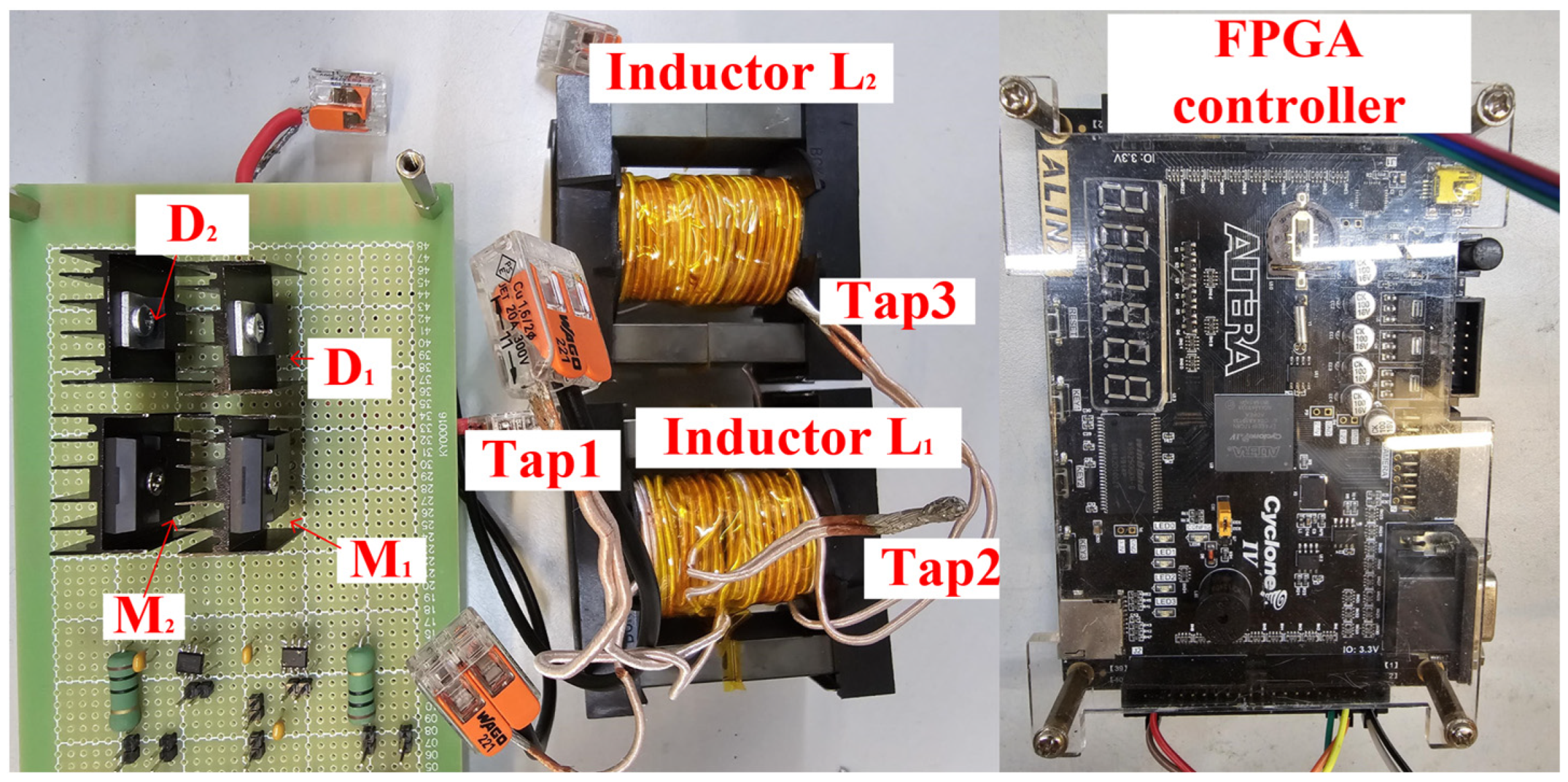
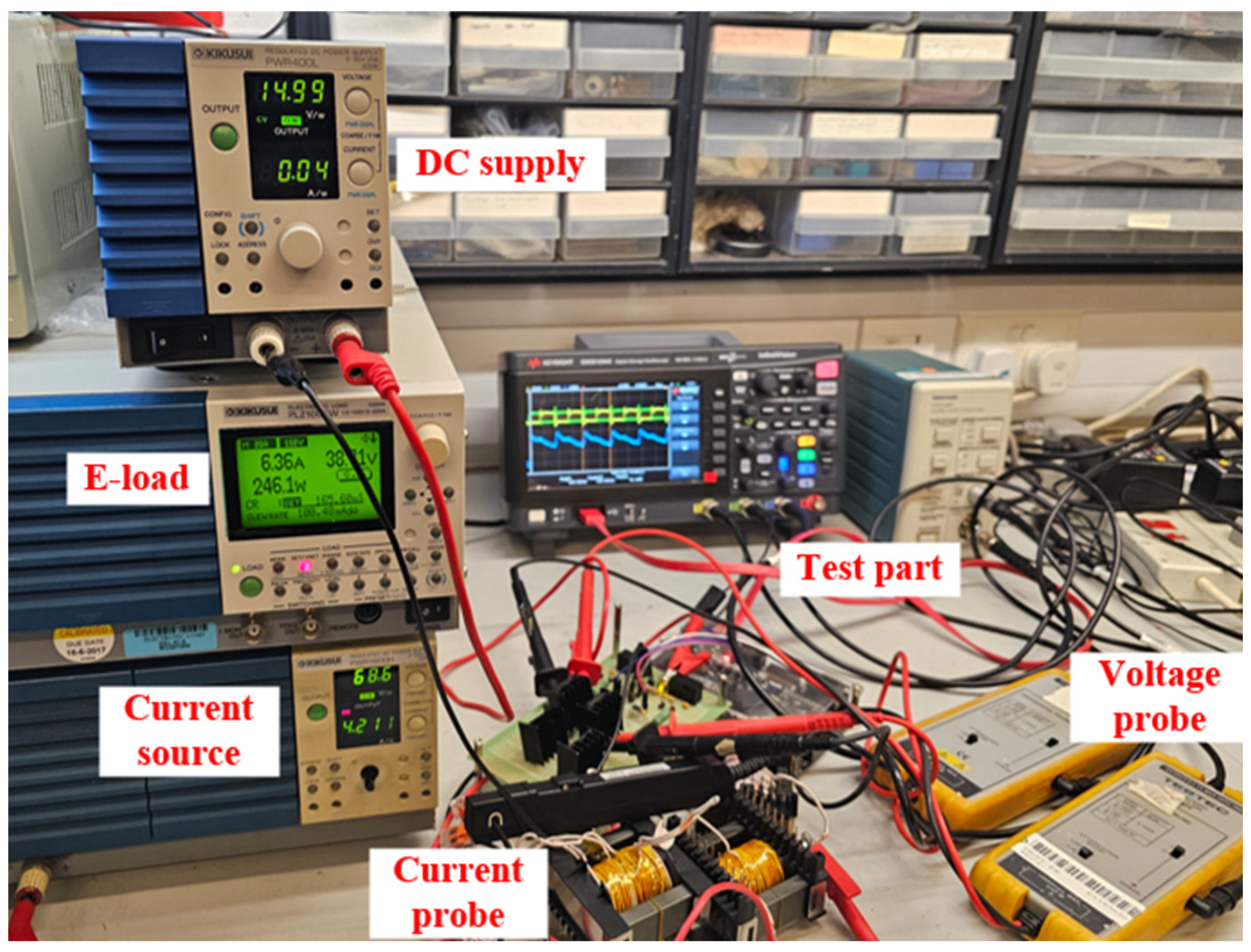
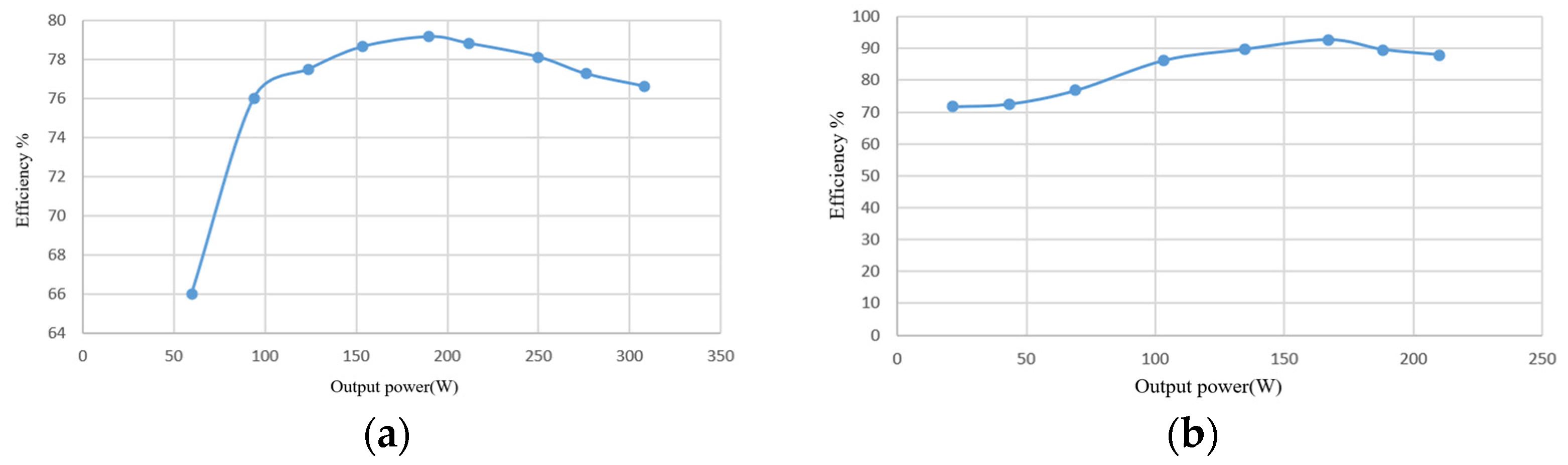
5. Prototype Experiments

Based on the simulation circuit, the FPGA obtains the 100 kHz signal and keeps the two signals with no dead time because it is a current-mode circuit; a current source open circuit is not allowed. The M1 and M2 plot in Figure 13 shows the detail. In addition, these two signals work in a complementary manner, but before one MOSFET turns off, the other MOSFET must turn on.
Under FPGA control, the parameters of the other components in the circuit and test equipment are shown in Table 2.
Inductor 1 is a tapped inductor; for the prototype experiments, it is just tapped at the 1/4, 1/2, and 3/4 position of the whole inductor’s winding length, so this inductor value can be 62.5 μH, 250 μH, 563 μH, and 1 mH in the proportional to the square of number of turns. The hardware circuit is shown in Figure 14, and the experimental platform is shown in Figure 15.
The experiment is performed firstly by connecting the circuit to a current source and then setting the input current to 4 A and the output load to 3.75 Ω and using an oscilloscope to read the GS signal of M2, the output current of the circuit, and the current at the middle-tapped point. This signal can be seen in Figure 16. The blue line shows the gate GS signal at 100 kHz, and the input dynamic voltage range is about 17.5 V. The red curve shows that the peak output current is about 6.62 A with an average of 6.37 A, and the current ripple is about 0.5 A. The yellow line shows that the tapped point with maximum current is 4 A; they are the same as the simulation.
The experiment is conducted by keeping the tapped point and the input current 4 A unchanged. The output resistance is varied using the electronic load in order to adjust the output power. Efficiency is measured at different power levels. Figure 17a shows the result versus the output power range from 60 W to 310 W. When the input power is about 200 W, it is the maximal power efficiency point at around 79%. The next set of experiments is for the output current at 3 A. When the tapped point remains unchanged, the input current is adjusted to 3 A, and the power is varied by adjusting the output resistance through the electronic load. The output power efficiency is better than the case when the input current is 4 A. When the input power is about 170 W, the efficiency is about 93%, as seen in Figure 17b. From these two figures, it is easy to see that for the present operation, when the input power is about 150 W to 200 W, the output power has better efficiency.
Figure 18 shows the experimental conversion ratio against the turn’s ratio under different input currents. It can be seen that the experimental conversion ratio agrees very well with the theory, and the ratio only decreases slightly with a higher current because of the higher current loss.

6. Conclusions

In this article, a tap-type current-mode converter control circuit is proposed, which can control the current mode output current in a range of one to two times the input current by controlling the tap point of the inductor. The utilization of inductor tapping offers an alternative method of current conversion that is simple and stable. The design provides an alternative manner to adjust the output current whilst the number of components used in the circuit is low. It maintains relatively good in its conversion efficiency within a specific range. In this paper, the principal design, analog simulation, and hardware testing were performed to prove the feasibility of the complete test. A conversion efficiency of 93% and 170 W output was achieved with an input current of 3 A. This circuit can be well utilized in small power supply circuits of up to 300 W. It provides a new solution for consumer electronics WPT, solar panels, and LED control circuits.

Author Contributions

Conceptualization, K.W.E.C.; Methodology, J.M.; Investigation, J.M. and T.H.; Resources, K.W.E.C.; Writing—original draft, J.M. and T.H.; Writing—review & editing, K.W.E.C. All authors have read and agreed to the published version of the manuscript.

Funding

The project is funded by the General Research Fund of the RGC University Grants Committee under project numbers 15207721 and 15225422.

Data Availability Statement

The original contributions presented in the study are included in the article.

Conflicts of Interest

The authors declare no conflict of interest.

References

  1. de Freitas, C.A.F.; Bartholomeus, P.; Margueron, X.; Le Moigne, P. Series Architecture for the Reduction of the DC-DC Converter in a Hybrid Energy Storage System for Electric Vehicles. Energies 2023, 16, 7620. [Google Scholar] [CrossRef]
  2. Cheng, K.W.E.; Ye, Y.M. Duality approach to the study of switched-inductor power converters and its higher-order variations. IET Power Electron. 2015, 8, 489–496. [Google Scholar] [CrossRef]
  3. Tatar, K.; Chudzik, P.; Leśniewski, P. Sliding Mode Control of Buck DC–DC Converter with LC Input Filter. Energies 2023, 16, 6983. [Google Scholar] [CrossRef]
  4. Nguyen, M.-K. Power Converters in Power Electronics: Current Research Trends. Electronics 2020, 9, 654. [Google Scholar] [CrossRef]
  5. Xu, C.; Cheng, K.W.E. Topology and Formation of Current Source Step Down Resonant Switched Inductor Converters. Energies 2022, 15, 1697. [Google Scholar] [CrossRef]
  6. Zhao, B.; Abramovitz, A.; Liu, C.; Yang, Y.; Huangfu, Y. A Family of Single-Stage, Buck-Boost Inverters for Photovoltaic Applications. Energies 2020, 13, 1675. [Google Scholar] [CrossRef]
  7. Mishra, N.; Singh, B.; Cheng, K.W.E. Power Quality Assessment of CPUC Based Solar Photovoltaic System with NLMS for Grid-Tied Applications. IEEE Trans. Power Deliv. 2023, 38, 655–665. [Google Scholar] [CrossRef]
  8. Chen, W.; Cheng, K.W.E.; Shao, J. Circuit Topology Analysis for LED Lighting and its Formulation Development. Energies 2019, 12, 4203. [Google Scholar] [CrossRef]
  9. Lee, H.-S.; Yun, J.-J. Three-Port Converter for Integrating Energy Storage and Wireless Power Transfer Systems in Future Residential Applications. Energies 2020, 13, 272. [Google Scholar] [CrossRef]
  10. Wang, X.; Cheng, K.W.E.; Fong, Y.C. Zero Current Switching Switched-Capacitors Balancing Circuit for Energy Storage Cell Equalization and Its Associated Hybrid Circuit with Classical Buck-Boost. Energies 2019, 12, 2726. [Google Scholar] [CrossRef]
  11. Vishnuram, P.; P, S.; R, N.; K, V.; Nastasi, B. Wireless Chargers for Electric Vehicle: A Systematic Review on Converter Topologies, Environmental Assessment, and Review Policy. Energies 2023, 16, 1731. [Google Scholar] [CrossRef]
  12. Szczepaniak, M.; Otręba, P.; Otręba, P.; Sikora, T. Use of the Maximum Power Point Tracking Method in a Portable Lithium-Ion Solar Battery Charger. Energies 2021, 15, 26. [Google Scholar] [CrossRef]
  13. Shieh, Y.-T.; Wu, C.-C.; Jeng, S.-L.; Liu, C.-Y.; Hsieh, S.-Y.; Haung, C.-C.; Shieh, W.-Y.; Chieng, W.-H.; Chang, E.-Y. A Turn-Ratio-Changing Half-Bridge CLLC DC–DC Bidirectional Battery Charger Using a GaN HEMT. Energies 2023, 16, 5928. [Google Scholar] [CrossRef]
  14. Li, H.; Yang, Y.; Chen, J.; Xu, J.; Liu, M.; Wang, Y. A Hybrid Class-E Topology With Constant Current and Constant Voltage Output for Light EVs Wireless Charging Application. IEEE Trans. Transp. Electrif. 2021, 7, 2168–2180. [Google Scholar] [CrossRef]
  15. Pan, X.; Ghoshal, A.; Liu, Y.; Xu, Q.; Rathore, A.K. Hybrid-Modulation-Based Bidirectional Electrolytic Capacitor-Less Three-Phase Inverter for Fuel Cell Vehicles: Analysis, Design, and Experimental Results. IEEE Trans. Power Electron. 2018, 33, 4167–4180. [Google Scholar] [CrossRef]
  16. Shafiqurrahman, A.; Umesh, B.S.; Sayari, N.A.; Khadkikar, V. Electric Vehicle-to-Vehicle Energy Transfer Using On-Board Converters. IEEE Trans. Transp. Electrif. 2023, 9, 1263–1272. [Google Scholar] [CrossRef]
  17. Leung, C.P.; Cheng, K.W.E. Design, Analysis and Implementation of the Tapped-Inductor Boost Current Converter on Current Based System. Energies 2021, 14, 888. [Google Scholar] [CrossRef]
  18. Salo, M.; Tuusa, H. A Vector-Controlled PWM Current-Source-Inverter-Fed Induction Motor Drive With a New Stator Current Control Method. IEEE Trans. Ind. Electron. 2005, 52, 523–531. [Google Scholar] [CrossRef]
  19. Himmelstoss, F.A.; Votzi, H.L. A family of quadratic DC/DC converters with one low-side switch and a tapped inductor at the output side. In Proceedings of the 2019 International Aegean Conference on Electrical Machines and Power Electronics (ACEMP) & 2019 International Conference on Optimization of Electrical and Electronic Equipment (OPTIM), Istanbul, Turkey, 27–29 August 2019. [Google Scholar]
  20. de Carvalho, M.R.S.; Barbosa, E.A.O.; Bradaschia, F.; Limongi, L.R.; Cavalcanti, M.C. Soft-Switching High Step-Up DC–DC Converter Based on Switched-Capacitor and Autotransformer Voltage Multiplier Cell for PV Systems. IEEE Trans. Ind. Electron. 2022, 69, 12886–12897. [Google Scholar] [CrossRef]
  21. Imanlou, A.; Najmi, E.S.; Behkam, R.; Nazari-Heris, M.; Gharehpetian, G.B. A New High Voltage Gain Active Switched-Inductor Based High Step-Up DC–DC Converter With Coupled-Inductor. IEEE Access 2023, 11, 56749–56765. [Google Scholar] [CrossRef]
  22. Tang, Y.; Fu, D.; Wang, T.; Xu, Z. Hybrid Switched-Inductor Converters for High Step-Up Conversion. IEEE Trans. Ind. Electron. 2015, 62, 1480–1490. [Google Scholar] [CrossRef]
  23. Scirè, D.; Lullo, G.; Vitale, G. Non-Linear Inductor Models Comparison for Switched-Mode Power Supplies Applications. Electronics 2022, 11, 2472. [Google Scholar] [CrossRef]
  24. Scirè, D.; Vitale, G.; Ventimiglia, M.; Lullo, G. Non-Linear Inductors Characterization in Real Operating Conditions for Power Density Optimization in SMPS. Energies 2021, 14, 3924. [Google Scholar] [CrossRef]
  25. Roberto, S.F.; Scirè, D.; Lullo, G.; Vitale, G. Equivalent Circuit Modelling of Ferrite Inductors Losses. In Proceedings of the 2018 IEEE 4th International Forum on Research and Technology for Society and Industry (RTSI), Palermo, Italy, 10–13 September 2018. [Google Scholar]
Figure 1. Classical switched-capacitor converter.
Energies 17 02204 g001
Figure 2. Converted from voltage mode to a current mode switched-inductor converter.
Energies 17 02204 g002
Figure 3. Double mode current type converter.
Energies 17 02204 g003
Figure 4. Tapped inductor current type converter.
Energies 17 02204 g004
Figure 5. First stage. Iin flows through M1 to L2. The difference between the L2 current and Iin flows through D1.
Energies 17 02204 g005
Figure 6. Second stage. Iin flows through M2 to L2. The difference between the L2 current and Iin flows through D2.
Energies 17 02204 g006
Figure 7. Output current conversion ratio.
Energies 17 02204 g007
Figure 8. B and C at the same point connect with the M2 source and D1 cathode.
Energies 17 02204 g008
Figure 9. Simulation result.
Energies 17 02204 g009
Figure 10. Tapped point B in the middle point of the inductor. (a) Test circuit; (b) test waveforms.
Energies 17 02204 g010
Figure 11. Points A and B connect to the M1 source and M2 source. (a) Test circuit; (b) test waveforms.
Energies 17 02204 g011
Figure 12. Higher order of conversion ratio circuit.
Energies 17 02204 g012
Figure 13. M1 and M2 signals.
Energies 17 02204 g013
Figure 14. Hardware circuit.
Energies 17 02204 g014
Figure 15. View of the experimental setup.
Energies 17 02204 g015
Figure 16. Oscilloscope signal.
Energies 17 02204 g016
Figure 17. The results of the measured efficiency. (a) Io = 4 A; (b) Io = 3 A.
Energies 17 02204 g017
Figure 18. Experimental conversion ratio with turns ratio.
Energies 17 02204 g018
Table 1. Duality translation.
Before Duality TranslationAfter Duality Translation
Energies 17 02204 i001 VEnergies 17 02204 i002 I
Energies 17 02204 i003 MEnergies 17 02204 i003 M
Energies 17 02204 i004 DEnergies 17 02204 i004 D
Energies 17 02204 i005 CEnergies 17 02204 i006 L
Energies 17 02204 i007 REnergies 17 02204 i007 R
ParallelSeries
DeltaStar
Table 2. Components and specifications for the circuit.
Name Values
Input current 4 A
M1 and M2 IRF530N
Switching frequency100 kHz
D1 and D2IDH10G120C5
Output resistance 4 Ω
L11 mH
L21 mH
ControllerFPGA EP4CE6F17C8N
Power supplyPWR1600H
LoadE-load PLZ1004W
Disclaimer/Publisher’s Note: The statements, opinions and data contained in all publications are solely those of the individual author(s) and contributor(s) and not of MDPI and/or the editor(s). MDPI and/or the editor(s) disclaim responsibility for any injury to people or property resulting from any ideas, methods, instructions or products referred to in the content.

