
Design and Optimization of the Heatsink of a Level 1 Electric Vehicle Charger

 , and
, and
Abstract
1. Introduction
2. Materials and Methods
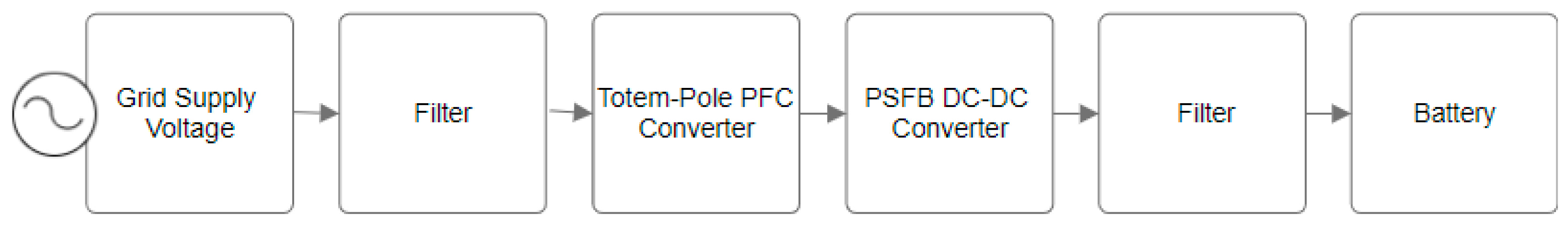
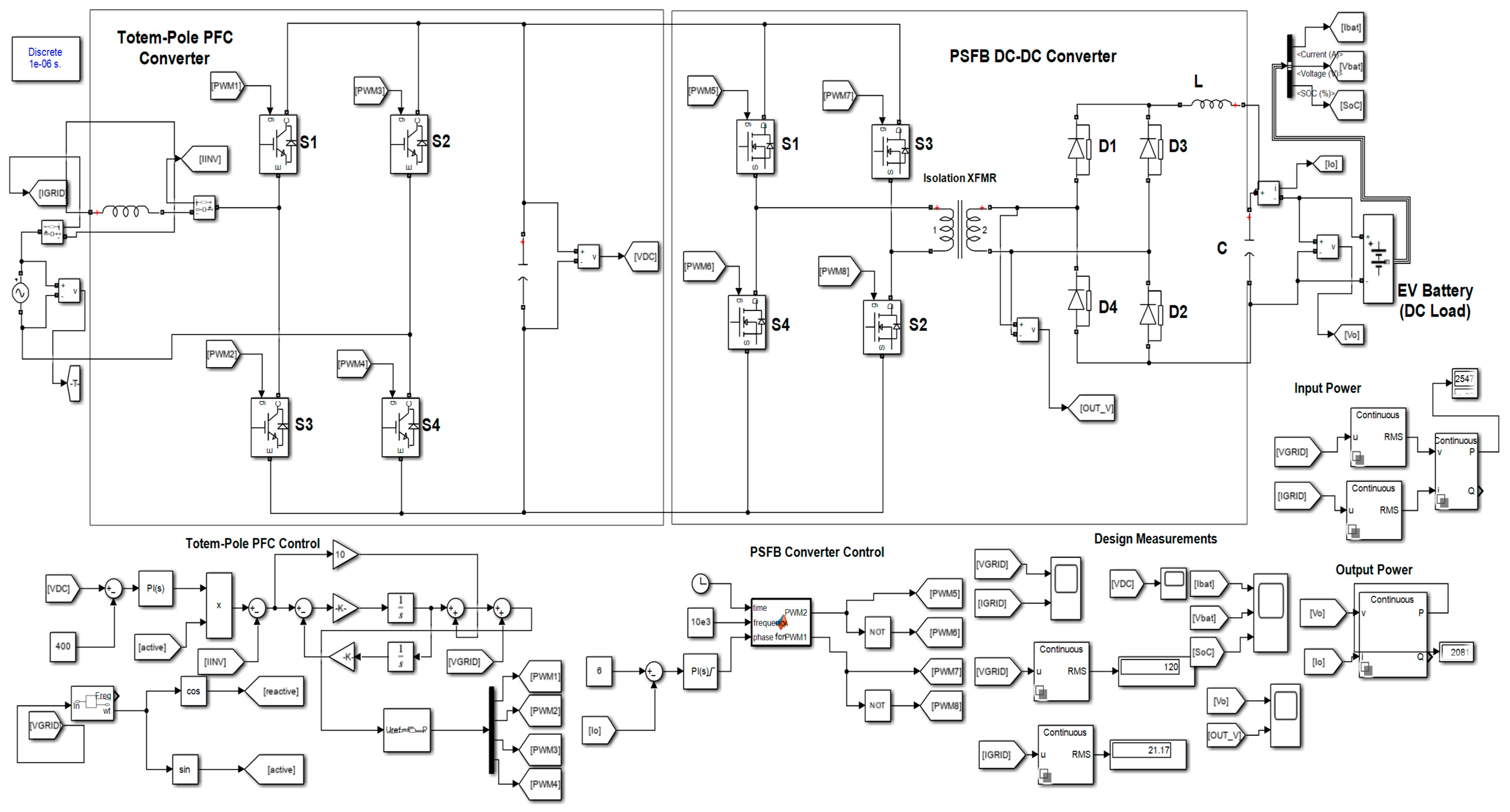
2.1. Summary of Charger Design Measurements
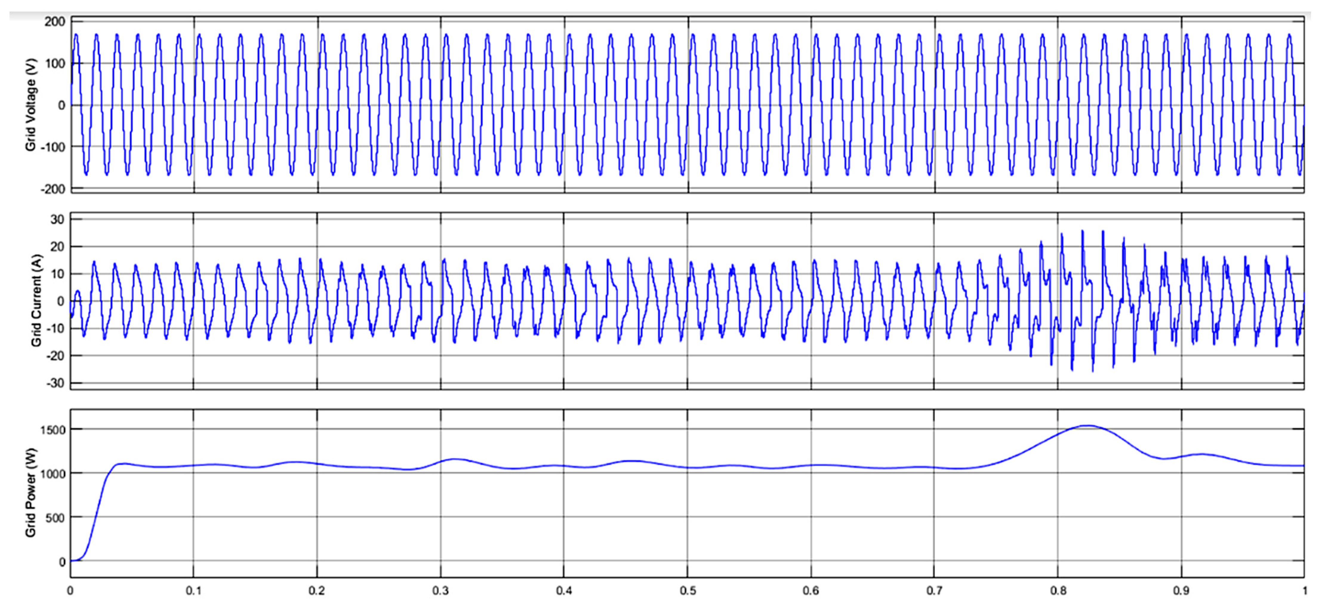
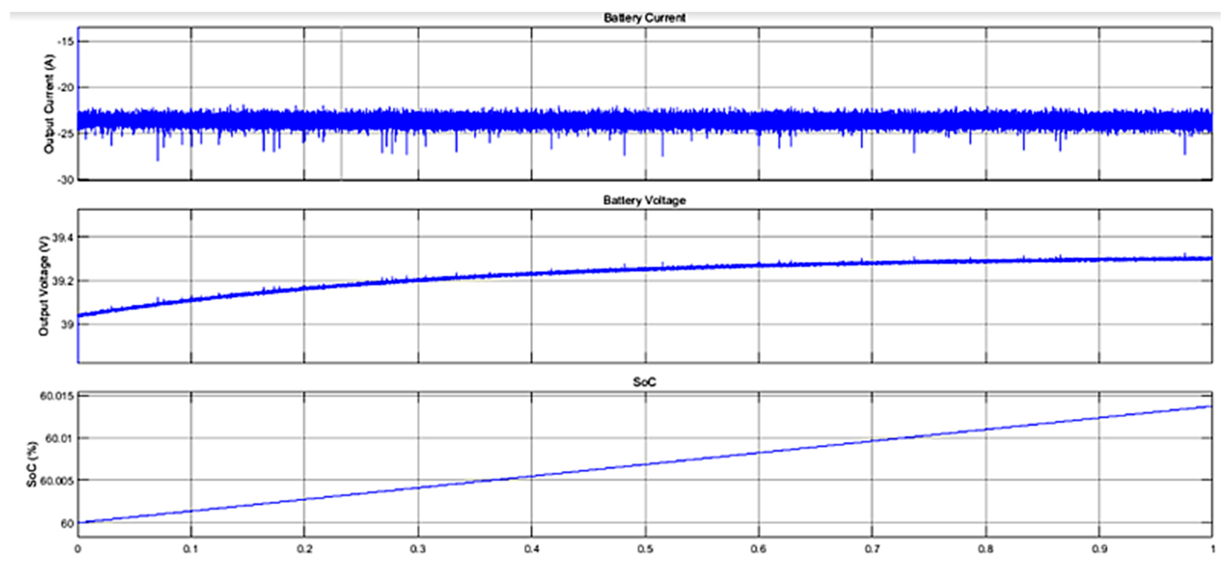
2.2. Charger Simulation Waveforms
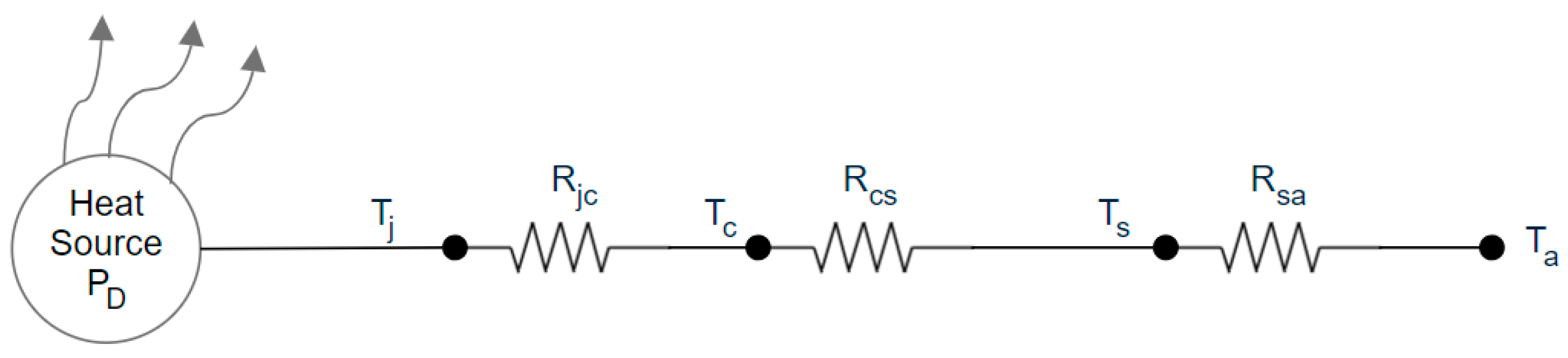
2.3. ANSYS Workbench Heatsink Model Design Parameters
- Ta = ambient temperature (25 °C);
- Tjmax = MOSFET maximum junction temperature defined on the manufacturer’s datasheet (150 °C);
- Rjc = junction-to-case thermal resistance (1.1 °C/W for S1/S2; 0.55 °C/W for S3–S8; 4 °C/W for D1–D4);
- Rcs = case-to-sink thermal resistance (0.8 °C/W) defined by the case–sink interface material and mounting compound assumed;
- Rsa = sink-to-ambient thermal resistance (°C/W);
- PD = power dissipation (W).
2.4. Transient Thermal Analysis Under Natural Convection Scenario
- Determines when the selected heatsink model cycles between the heating and cooling phases;
- Assesses the behavior of the model in response to a time-dependent heat load or bulk temperature;
- Assesses the components’ behavior under thermal stresses arising from temperature changes.
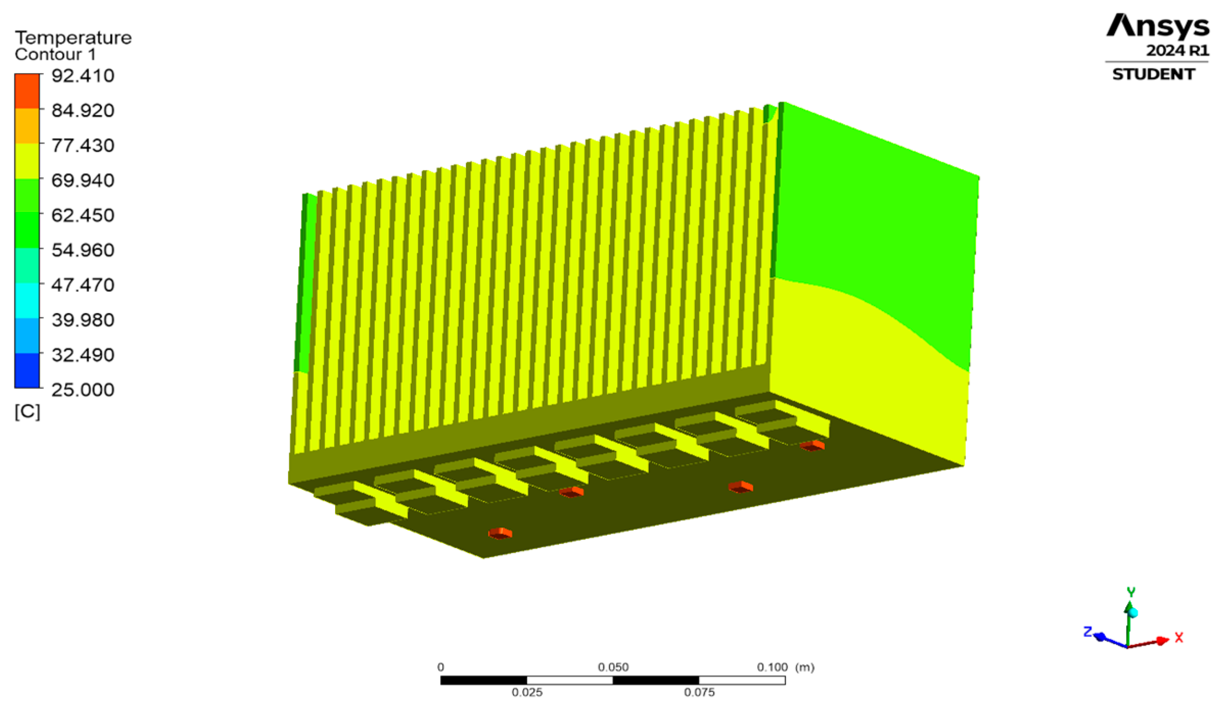
3. Results and Discussion of the Natural Cooling Scenario
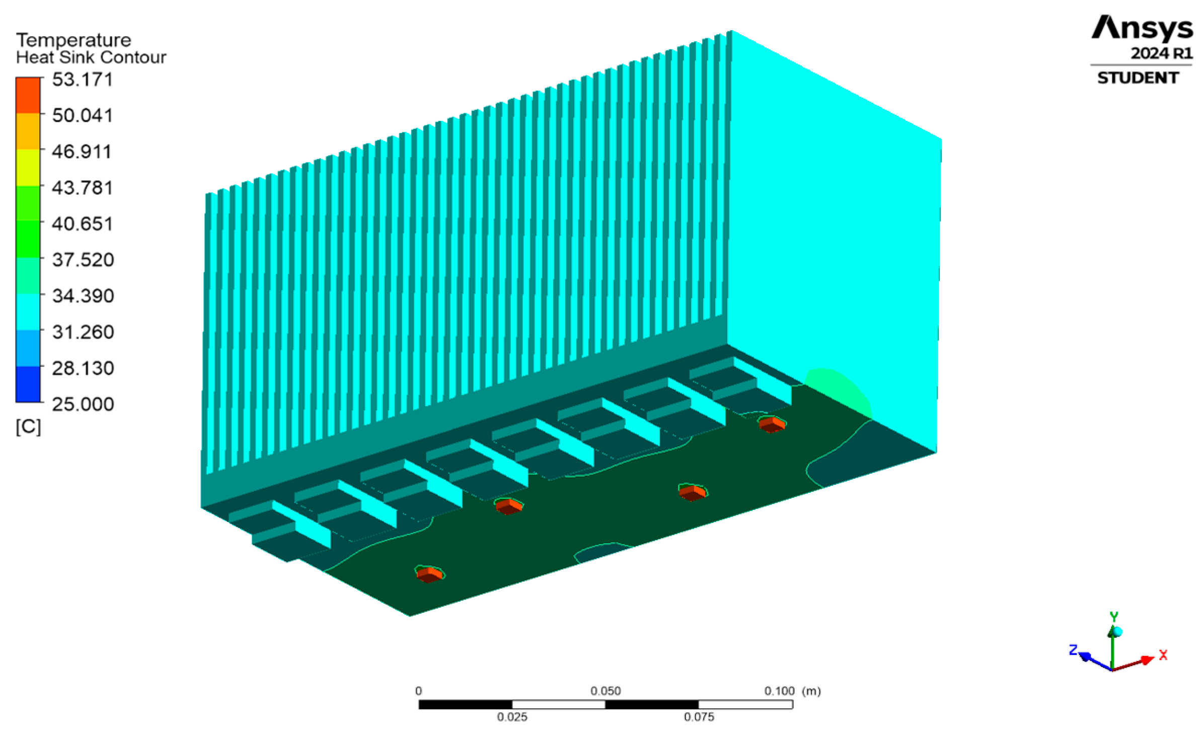
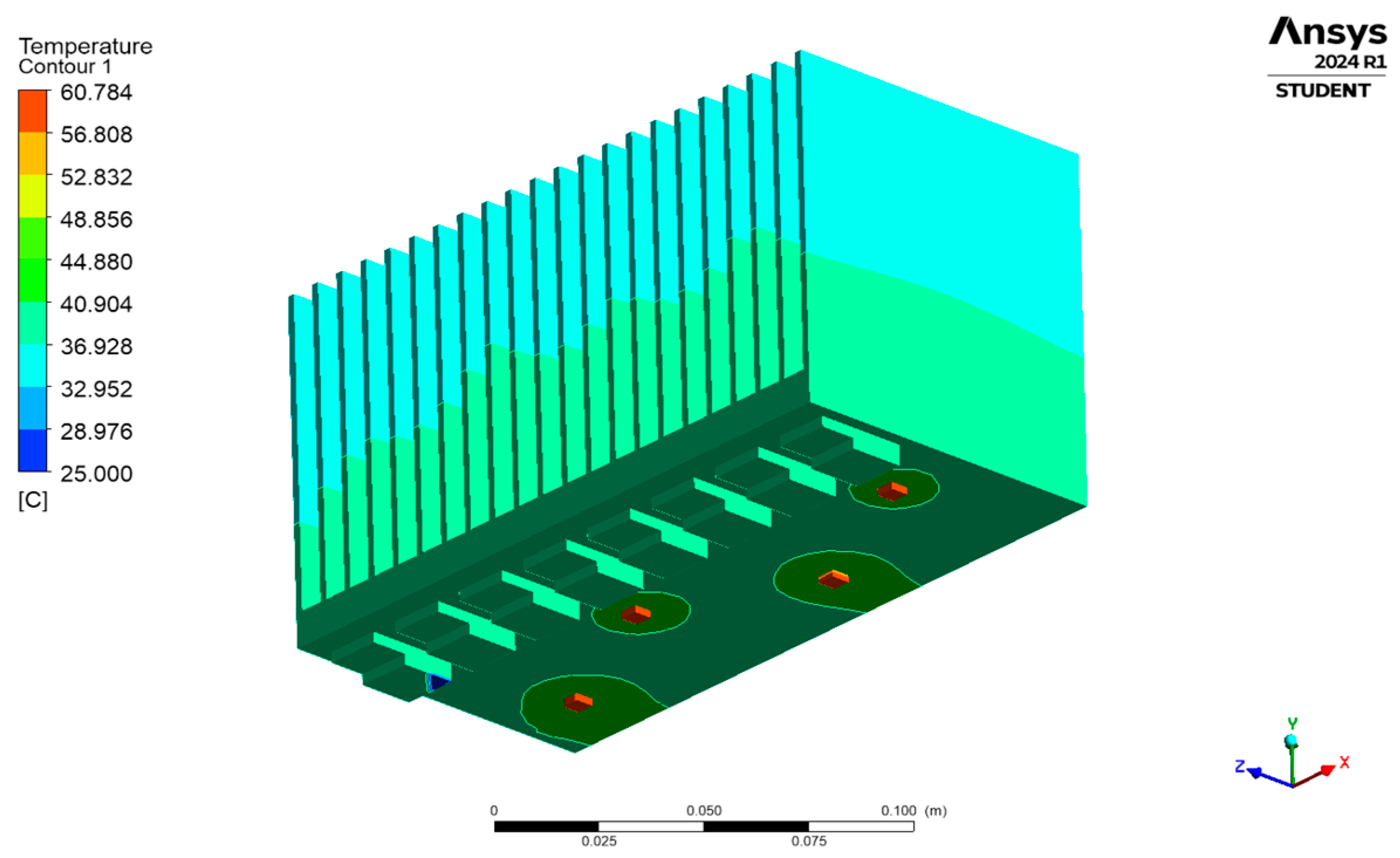
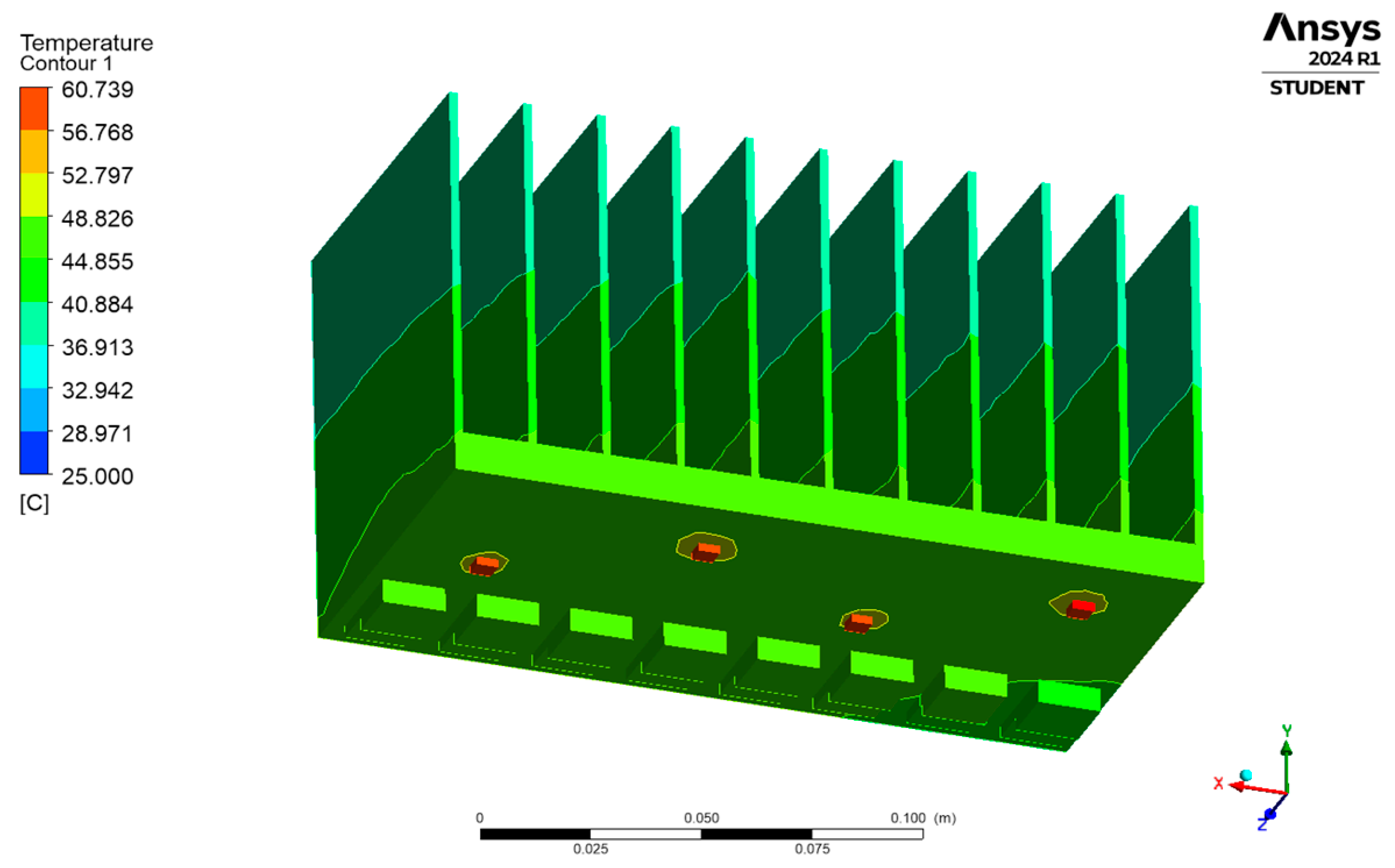
4. Results of Transient Thermal Analysis Under the Forced Convection Scenario
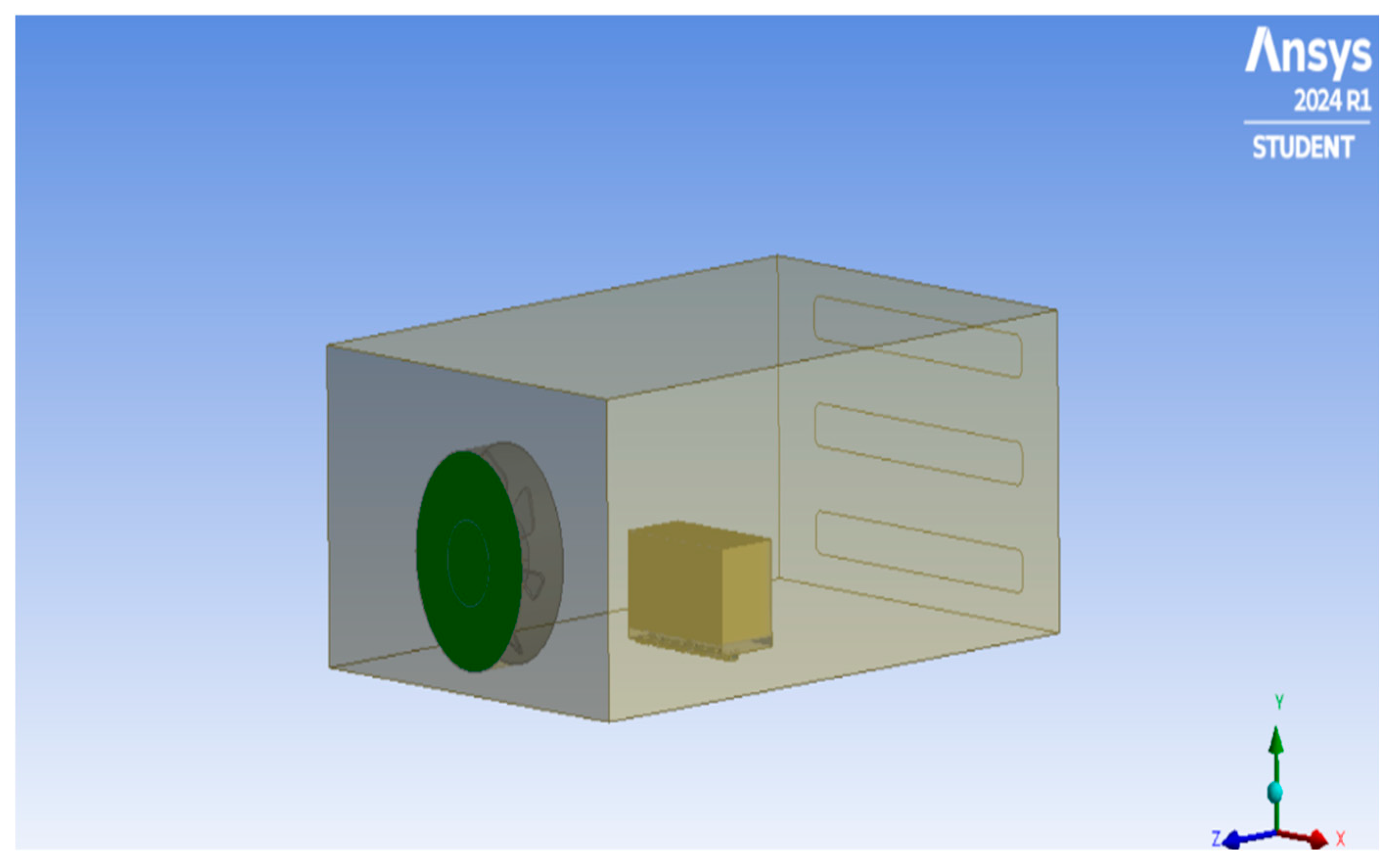
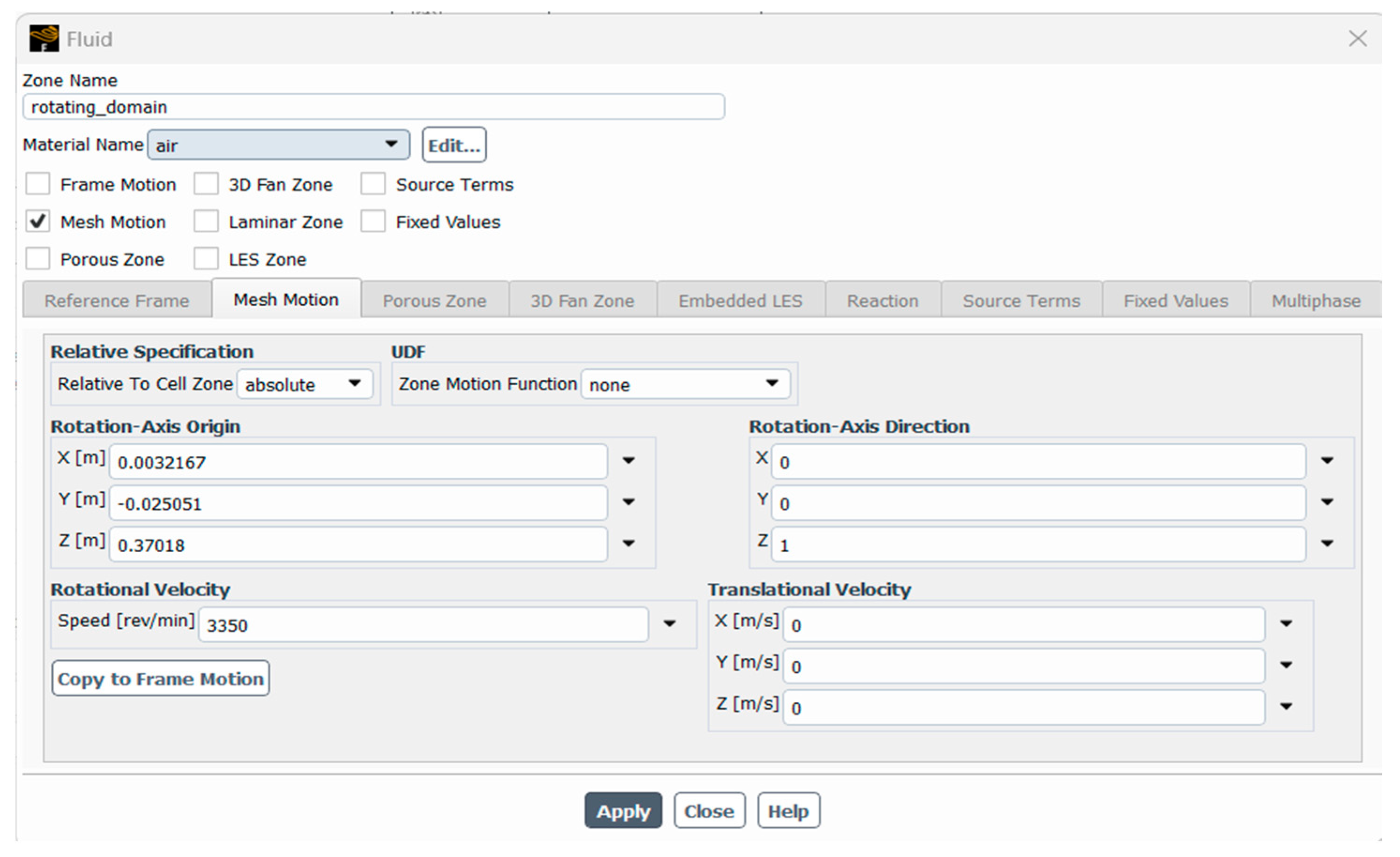
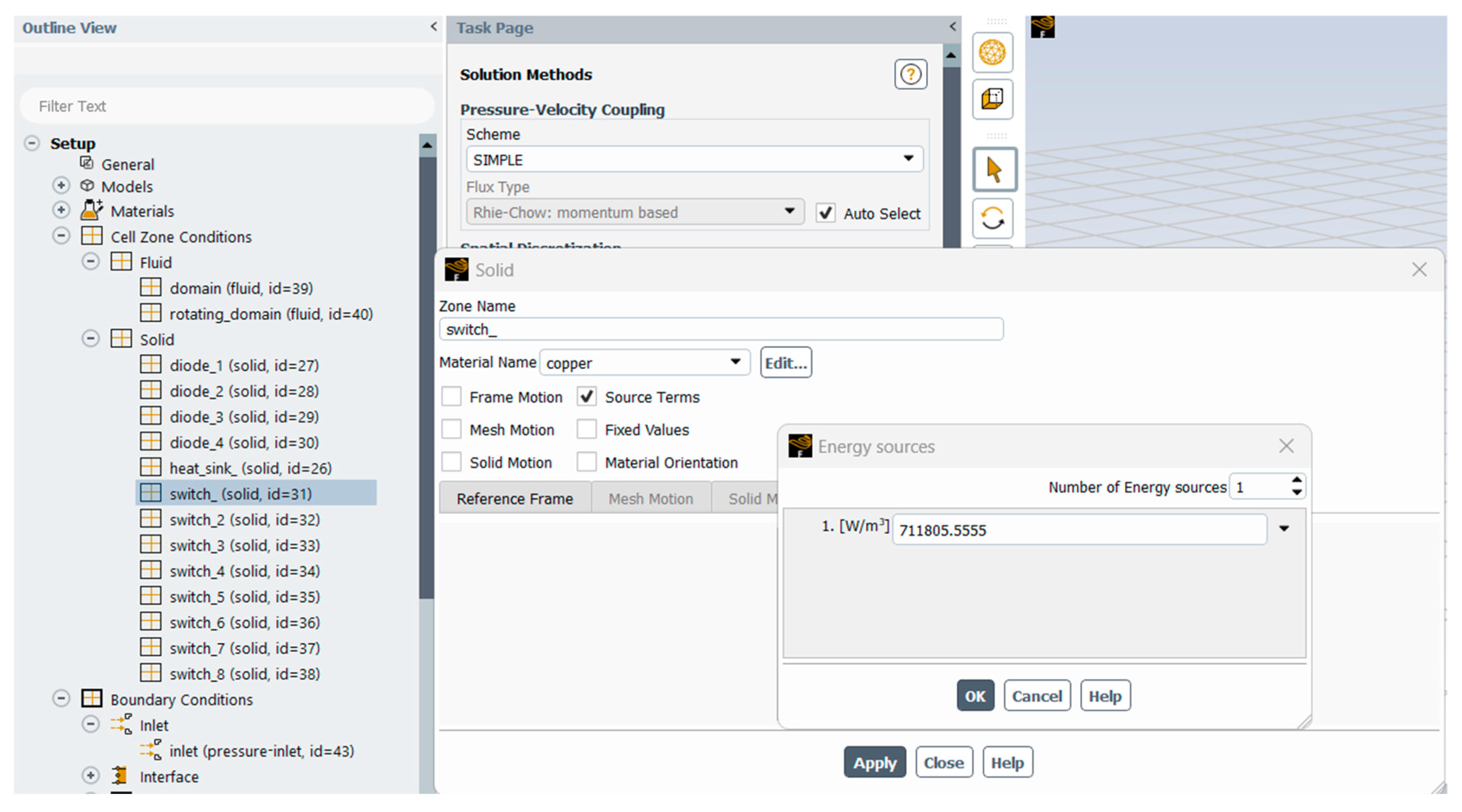
4.1. ANSYS Fluent Setup for Forced Cooling Analysis
- Geometry Modification: The model was further modified to separate the fluid and solid domains and to specify the inlet and outlet surfaces in the ANSYS software. The ANSYS tool called “DesignModeler” was used to edit the model.
- Meshing independence study: The computational domain was discretized into 562,095 mesh elements (and 179,314 node elements with size set as 51.041 mm) with increasing levels of refinement to solve the discretized fluid flow equations. The refinement display style selected was the orthogonal quality, with a maximum and minimum value of 1.0 and 0.066216, respectively. The relevant discretized equations of fluid flow for the mesh setup, which describe the motion of the fluid (air), are governed by the Navier–Stokes equations (principles of conservation of mass, momentum, and energy); they include (a) the continuity equation, which is given in Equations (3) and (4) for incompressible flows as follows:
- ;
- ;
- ;
- ;
- ;
- .
- (a)
- The momentum equation (Newton’s Second Law), which denotes the balance of forces on the fluid for incompressible flow, is given in Equation (5) as
- F = external forces (acceleration due to gravity);
- P = air pressure;
- = constant dynamic viscosity, representing its resistance to deformation;
- u = velocity vector.
- (b)
- The energy equation (conservation of energy in the fluid) for active cooling with heat transfer is given in Equation (6) as
- h = enthalpy;
- T = temperature;
- k = thermal conductivity of the sink material;
- Sh = source term of the heat generated by electronic components or fans.
4.2. Cell Zone, Power Density, Reynolds Number, and Nusselt Number Specification
- ;
- ;
- (90 mm from Table 2);
- .
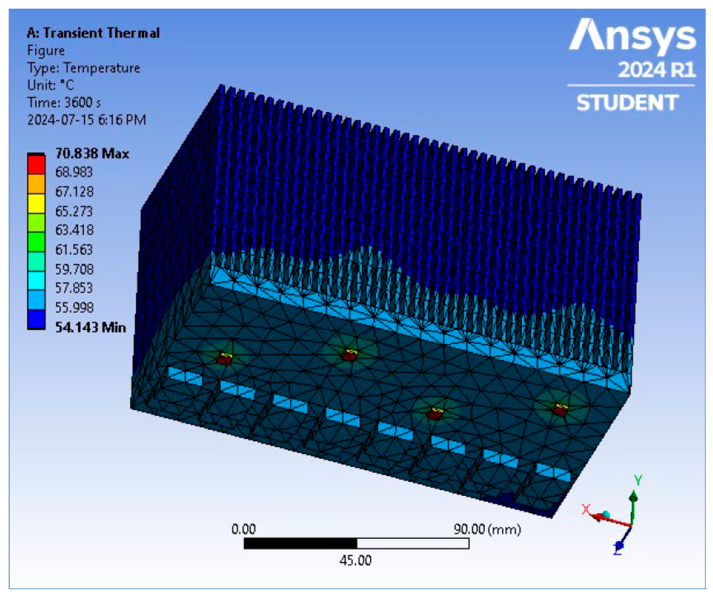
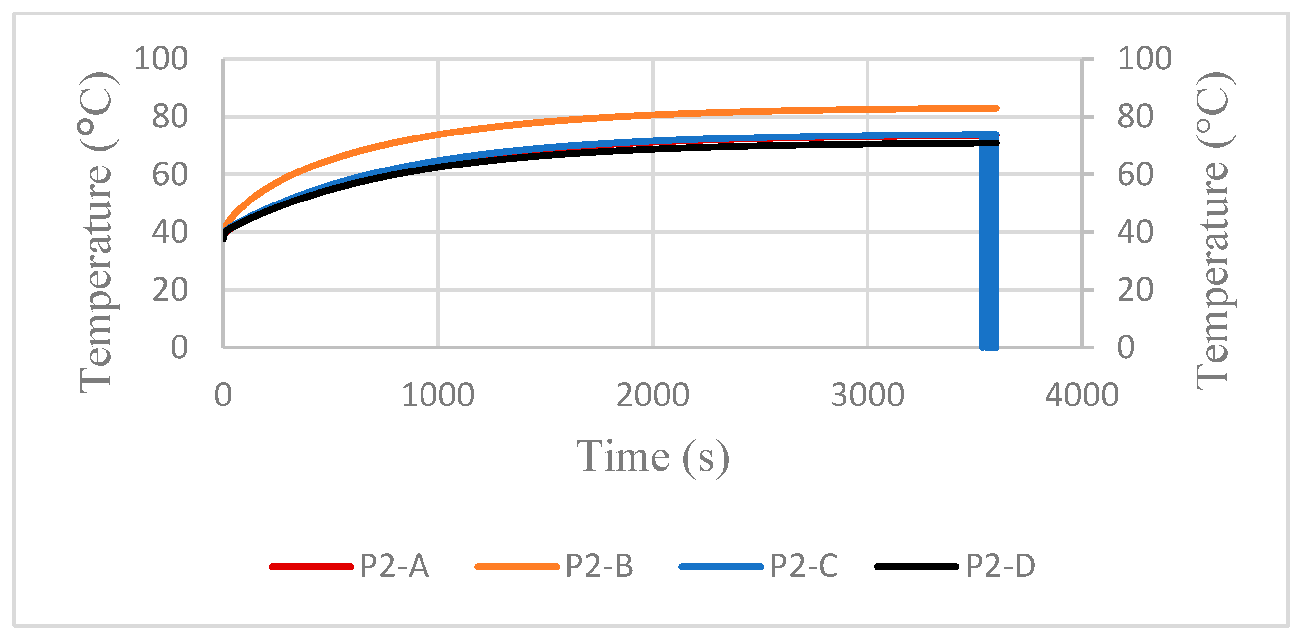
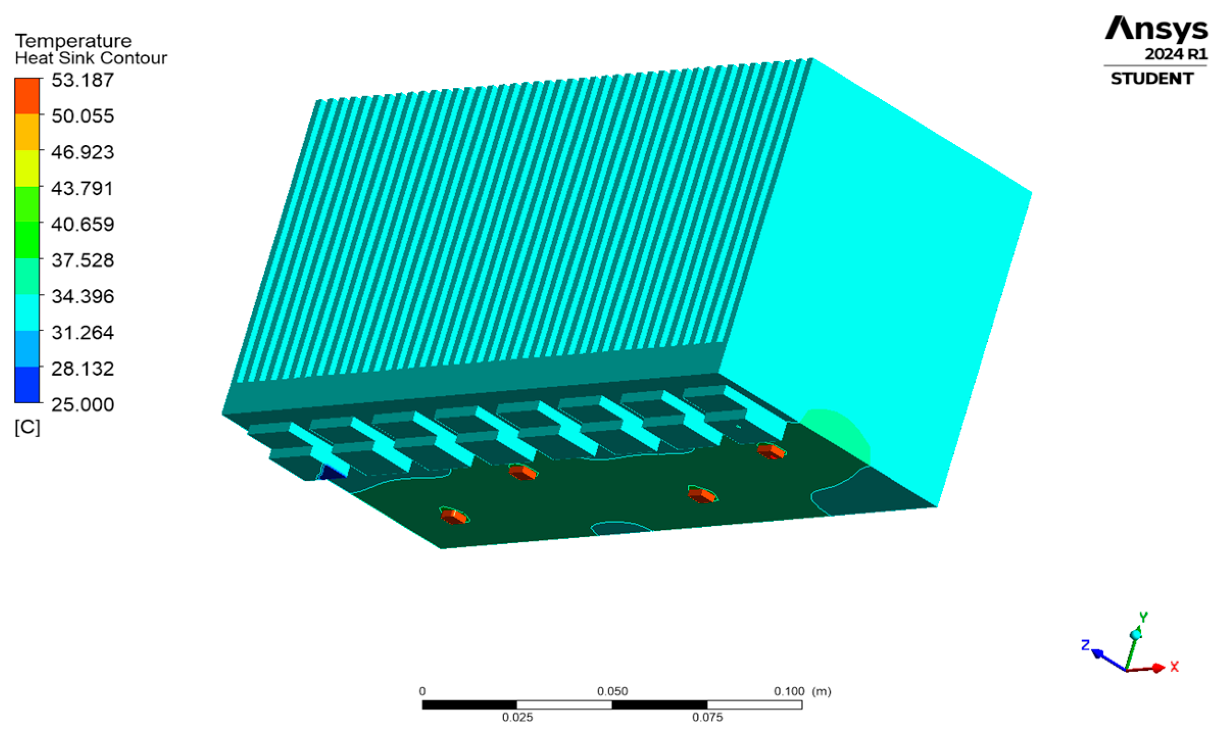
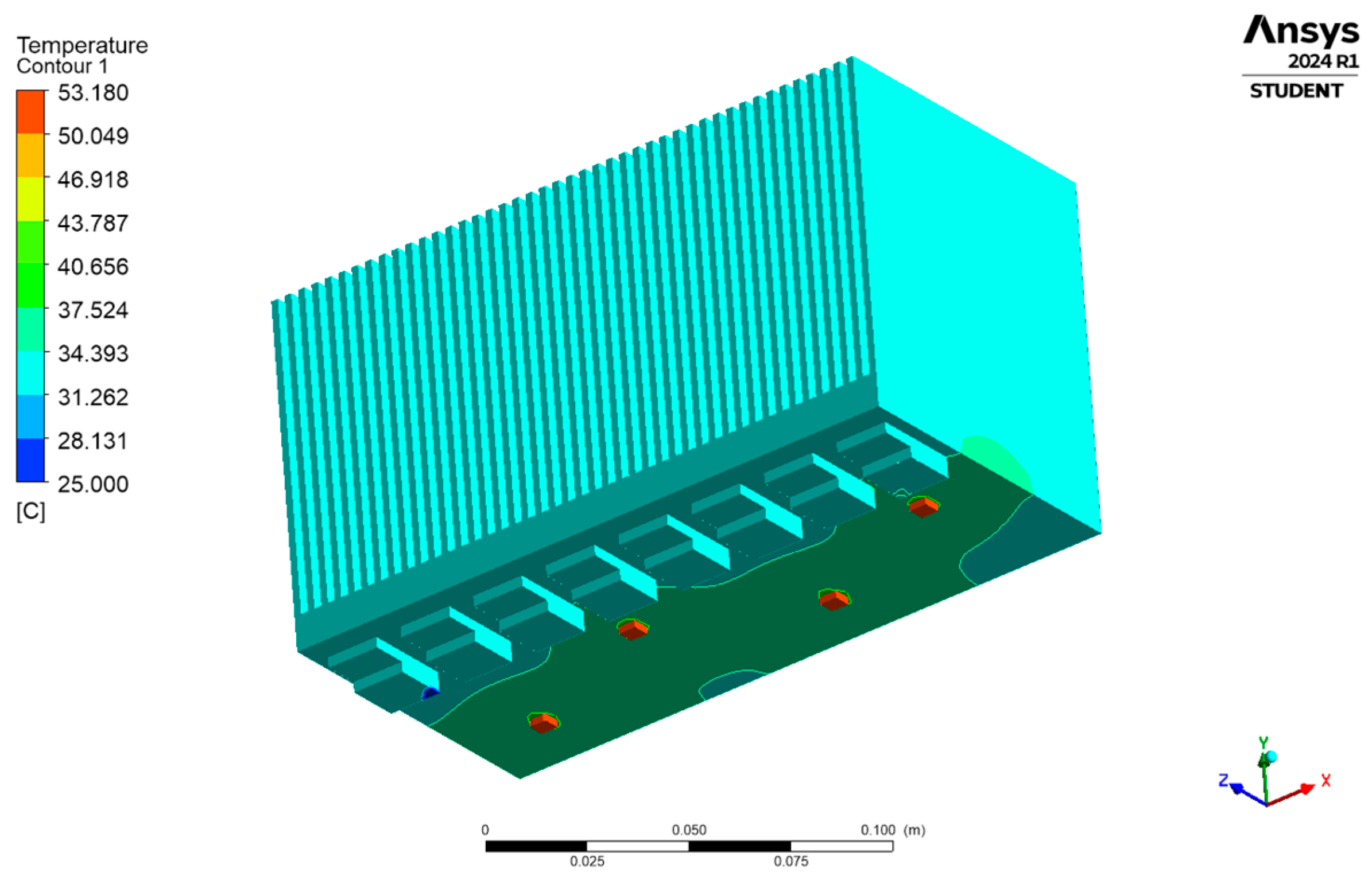
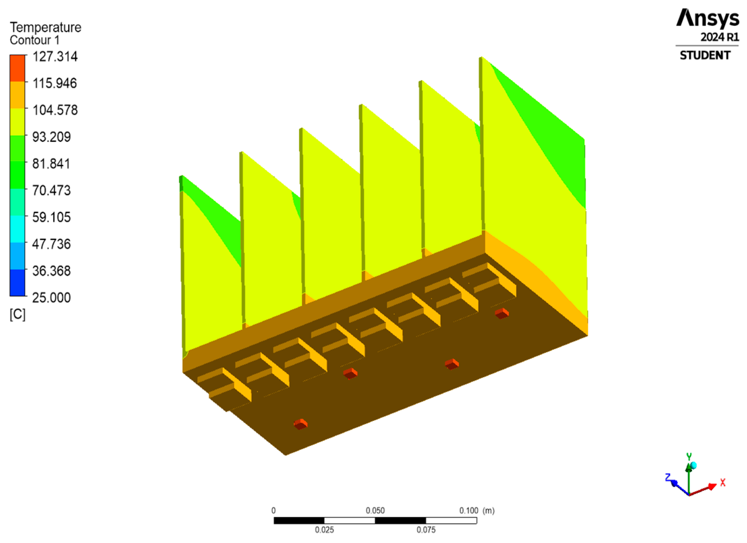
4.3. Transient Thermal Analysis Under Forced Convection Scenario
4.4. Comparative Analysis of Variants’ Thermal Performance Versus Fin Material Cost
5. Conclusions
- Fin Geometry and Thickness: Plate-fin geometries (models P1 and P2) demonstrated superior thermal dissipation compared to circular-fin designs (models C1 and C2), due to their larger surface area and linear configurations, which enhanced heat transfer through convection and radiation. Thinner fins (P2 with 2 mm thickness) improved heat transfer to the ambient by optimizing the fluid flow channels and increasing the effective heat transfer surface area.
- Switch and Diode Arrangement: The arrangement of heat-generating components on the heatsink significantly influenced thermal performance. Model P2-D, with an optimized layout of switches and diodes, reduced the maximum temperatures of switches by 14% and diodes by 4%, compared to unoptimized layouts. This highlights the importance of proper spacing to avoid localized hotspots and ensure a uniform heat distribution.
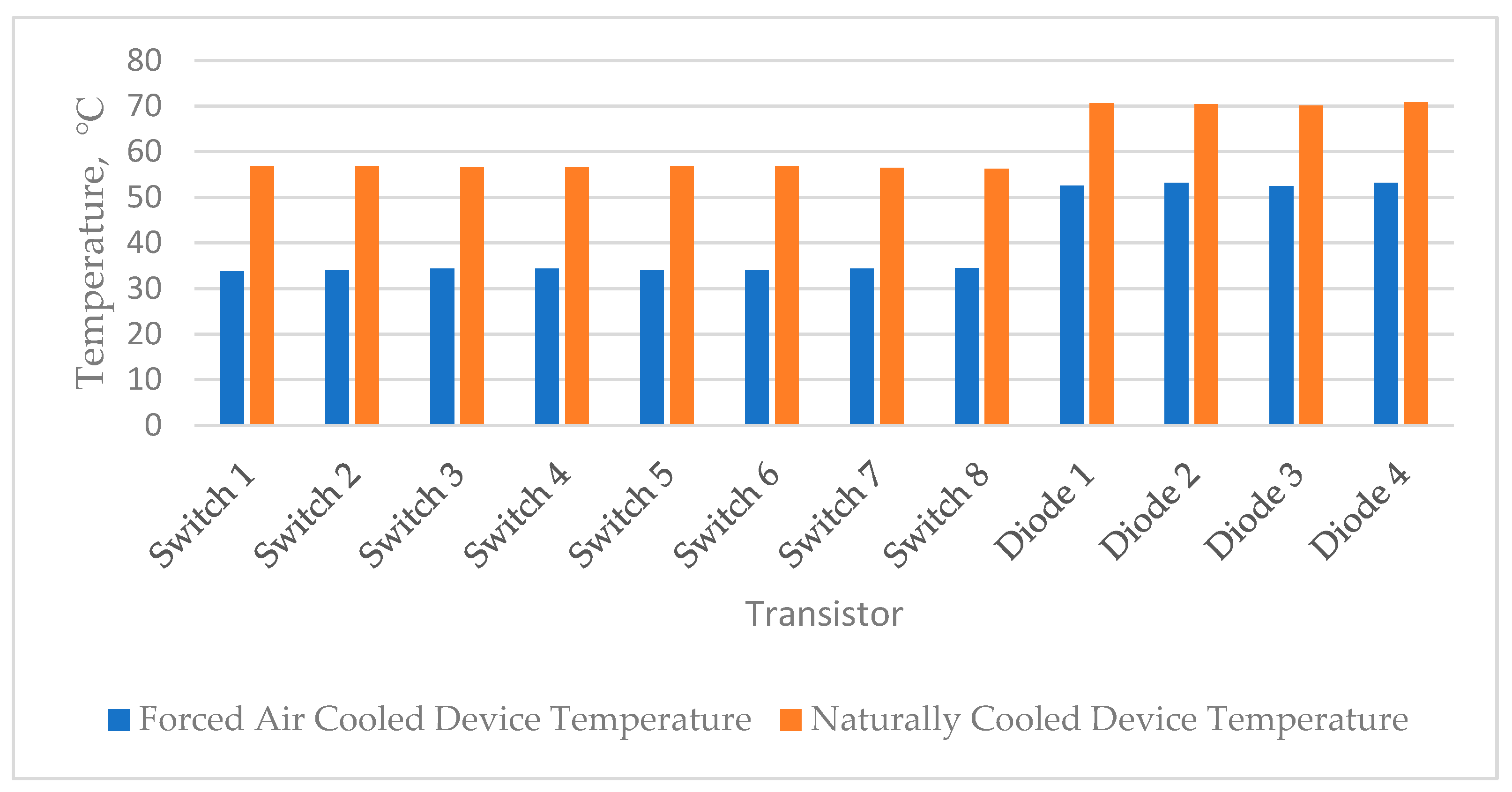
- Cooling Methods: Forced convection with a fan drastically improved thermal performance compared to natural convection. The maximum temperature of switch S1 decreased by 40.7% (from 56.87 °C under natural cooling to 33.73 °C under forced cooling), and diode D4 saw a 24.9% reduction in temperature. The optimal fan proximity (300 mm) ensured the best thermal dissipation without compromising airflow dynamics.
- Optimization of Fin Count: A 44-fin heatsink (model P2-D) exhibited the best thermal dissipation, with a balanced cost–performance tradeoff. Variants with reduced fin counts (e.g., 33 fins or 22 fins) showed diminishing returns on heat dissipation efficiency, further emphasizing the importance of balancing geometry with thermal requirements.
- Economic Feasibility: This study evaluated the cost-effectiveness of heatsink designs by analyzing the relationship between aluminum mass and cooling efficiency. Model P2-D was the most efficient design, achieving a superior thermal performance at 8.596 °C/$C of aluminum sink material with 44 fins compared to the 6-fin model with a thermal performance of 62.40 °C/$C.
6. Results’ Validation
- Zhang et al. [19] investigated natural convection heatsinks for battery chargers using various fin geometries and found that surface anodization improved the cooling efficiency by 27%. That aligns with this study’s findings that increasing the fin surface area and optimizing the geometry (thinner plate fins) enhance heat dissipation.
- Palumbo et al. [21] found that topologically optimized heatsinks achieved a 25% reduction in surface temperature when using additive manufacturing. While the authors did not employ advanced manufacturing techniques, the observed performance improvement reached 40% under forced convection, suggesting that simpler designs, combined with fan cooling, can achieve comparable results.
- Moradikazerouni et al. [24] found that increasing the fin height and count improved the cooling performance in laminar forced convection, and the present study confirmed this, demonstrating better cooling with 44 fins compared to reduced fin counts under forced convection conditions.
7. Novelty of This Study
- Focus on Switch and Diode Layout Impact: Unlike many previous studies, this research examines explicitly how the arrangement of MOSFETs and diodes on a heatsink affects thermal performance. This is a relatively unexplored factor in heatsink optimization for EV chargers. Some of the reviewed literature focuses on material-based thermal enhancements like phase change materials (PCMs) and thermal conductivity enhancers to address the heat dissipation capacity of the heatsink material. Unlike this study, it does not investigate the spatial arrangement of heat-generating electronic components. Furthermore, naturally cooled heatsinks for EV battery chargers focusing solely on fin geometry and surface modifications (e.g., anodization) have previously been studied. While the sink geometry in these studies was optimized, there was no attention to how the placement of diodes or MOSFETs might influence localized heat dissipation. This manuscript addresses that significant gap by demonstrating that the spatial layout of switches and diodes can significantly influence heat distribution. The results show that Model P2-D with an optimized layout reduces temperatures by 14% for switches and 4% for diodes, a clear improvement over unoptimized layouts.
- Integrating Natural and Forced Cooling Scenarios: This study evaluated natural convection and forced cooling scenarios to identify the best-performing heatsink design. It was unique in its thoroughness in combining these cooling methods with detailed simulation results.
- Comparative Analysis of Multiple Configurations: We performed an exhaustive comparative analysis by testing various heatsink geometries (circular and plate fins) and adjusting parameters like fin count, spacing, and proximity to a cooling fan. The findings reveal a specific optimal configuration (P2-D) that outperforms others.
- Comprehensive Thermal Simulation: Advanced simulation tools like ANSYS Workbench for transient thermal analysis, coupled with MATLAB/Simulink modeling of the EV charger, ensure high accuracy and applicability of the results.
- Thermal Efficiency vs. Cost Tradeoff: This study uniquely evaluated the cost-effectiveness of heatsink materials (aluminum) and geometries, ensuring their practical feasibility for manufacturers. This adds an economic dimension to the engineering problem.
Author Contributions
Funding
Data Availability Statement
Conflicts of Interest
Abbreviations
| CAD | Computer-Aided Design |
| CFD | Computational Fluid Dynamics |
| DC | Direct Current |
| EV | Electric Vehicle |
| ICE | Internal Combustion Engine |
| MOSFET | Metal-Oxide-Semiconductor Field-Effect Transistor |
| MW | Mega Watt |
| PCM | Phase Change Material |
| PD | Power Dissipated |
| PFC | Power Factor Correction |
| PSFB | Phase Shift Full Bridge |
| Rcs | Thermal Resistance of Case–Sink |
| RDS | Drain-Source Resistance |
| Rjc | Thermal Resistance of the Junction Case |
| Rsa | Thermal Resistance of Sink-Ambient |
| Ta | Ambient Temperature |
| Tc | Case Temperature |
| TJmax | Maximum Junction Temperature |
| Ts | Sink Temperature |
References
- Hemavathi, S.; Shinisha, A. A study on trends and developments in electric vehicle charging technologies. J. Energy Storage 2022, 52, 105031. [Google Scholar] [CrossRef]
- Doucette, R.T.; McCullooch, M.D. Modeling the prospects of plug-in hybrid electric vehicles to reduce CO2 emissions. Appl. Energy 2021, 88, 2315–2323. [Google Scholar] [CrossRef]
- Yadlapalli, R.; Kotapati, A.; Kandipati, R. A review on energy efficient technologies for electric vehicle applications. J. Energy Storage 2022, 50, 104212. [Google Scholar] [CrossRef]
- Aggarwal, S.; Singh, A. Electric vehicles the future of transportation sector: A review. Energy Sources, Part A: Recovery, Utilization, and Environmental Effects. J. Energy Sources 2021, 1976322. [Google Scholar] [CrossRef]
- Bigazzi, A.; Wong, K. Electric bicycle mode substitution for driving, public transit, conventional cycling, and walking. Transp. Res. Part D Transp. Environ. 2020, 85, 102412. [Google Scholar] [CrossRef]
- Bhagvati, S.; Kohli, P.; Kulkarni, D.; Pandey, K.; Rizvi, Z. Optimization of surface area of heat sink using design for additive manufacturing. Mater. Today Proc. 2024, 1–6. [Google Scholar] [CrossRef]
- Seshasayee, N. Understanding Thermal Dissipation and Design of a Heatsink; Texas Instruments: Austin, TX, USA, 2011. [Google Scholar]
- Ghorbani, M.; Wang, H.; Roberts, N. Analytical and numerical modeling of phase change material and hybrid PCM-heat sinks for high-power wireless EV charging. Int. Commun. Heat Mass Transf. 2024, 154, 107460. [Google Scholar] [CrossRef]
- Nai, V.; Baby, A.; Anoop, M.B.; Indrajith, S.; Murali, M.; Nair, M. A comprehensive review of air-cooled heat sinks for thermal management of electronic devices. Int. Commun. Heat Mass Transf. 2024, 159, 108055. [Google Scholar]
- Gaikwad, A.; Sathe, A.; Sanap, S. A design approach for thermal enhancement in heat sinks using different types of fins: A review. Front. Therm. Eng. 2023, 2, 980985. [Google Scholar] [CrossRef]
- Maha, H.; Talal, H. The Optimal Design of Heat Sinks: A Review. J. Comput. Mech. 2019, 6, 1030–1043. [Google Scholar]
- Khudhur, D.; Al-Zuhairy, R.; Kassim, M. Thermal analysis of heat transfer with different fin geometry through straight plate-fin heat sinks. Int. J. Therm. Sci. 2022, 174, 107443. [Google Scholar] [CrossRef]
- Foronda, E.; Ramirez-Gil, F.; Delgado-Mejia, A.; Ballesteros, L.; Rudas, J.; Olmos-Villalba, L. Thermal enhancement of heat sinks with bio-inspired textured surfaces. Therm. Sci. Eng. Prog. 2023, 46, 102170. [Google Scholar] [CrossRef]
- Zhao, W.; Mercier, D. Materials Selection for a Heat Sink. In Ansys Educational Resources; Ansys Academic Development Team: Canonsburg, PA, USA, 2022. [Google Scholar]
- Akinluwade, K.; Omole, R.; Isadare, A.; Adesina, O.; Adetunji, A. Material Selection for heat Sinks in HPC Mocrochip-Based Circuitries. Br. J. Appl. Sci. Technol. 2015, 7, 124–133. [Google Scholar] [CrossRef]
- Ahmed, H.; Salman, B.; Kherbeet, A.; Ahmed, M. Optimization of thermal design of heat sinks: A review. Int. J. Heat Mass Transf. 2018, 150, 1079–1089. [Google Scholar] [CrossRef]
- Shaeri, M.; Bonner, R., II. Analytical heat transfer model for laterally perforated-finned heat sinks. Int. J. Heat Mass Transf. 2019, 131, 1164–1173. [Google Scholar] [CrossRef]
- Miguel, A. Optimal Y-shaped constructs heat sinks under different size constraints. Int. J. Heat Mass Transf. 2019, 131, 64–71. [Google Scholar] [CrossRef]
- Zhang, Z.; Lau, E.; Botting, C.; Bahrami, M. Naturally cooled heat sinks for battery chargers. Int. J. Heat Mass Transf. 2020, 147, 118911. [Google Scholar] [CrossRef]
- Han, F.; Guo, H.; Ding, X. Design and Optimization of a Liquid Cooled Heat Sink for a Motor Inverter in Electric Vehicles. Appl. Energy 2021, 291, 116819. [Google Scholar] [CrossRef]
- Palumbo, J.; Tayyara, O.; Assadi, S.A.; Da Silva, C.M.; Trecases, O.; Amon, C.H.; Chandra, S. Implementation of a Topologically Optimized Heat Sink for Non-Uniform Heat Fluxes in an Electric-Vehicle fast-Charger. In Proceedings of the 22nd IEEE Intersociety Conference on Thermal and Thermomechanical Phenomena in Electronic Systems, Orlando, FL, USA, 30 May–2 June 2023. [Google Scholar]
- Rasool, H.; Vergrugge, B.; Zhaksylyk, A.; Tran, T.M.; Baghdadi, M.E.; Geury, T. Design Optimization of an Off-Board Charging System for Electric Bus Applications. IEEE Access 2021, 9, 84501–84519. [Google Scholar] [CrossRef]
- Mozafari, M.; Lee, A.; Mohammadpour, J. Thermal management of single and multiple PCMs based heat sinks for electronics cooling. J. Therm. Sci. 2021, 23, 100919. [Google Scholar] [CrossRef]
- Moradikazerouni, A.; Afrand, M.; Jalal, A.; Wongwises, S.; Asadi, A.; Nguyen, T. Investigation of a computer CPU heat sink under laminar forced convection using a structural stability method. Int. J. Heat Mass Transf. 2019, 134, 1218–1226. [Google Scholar] [CrossRef]
- Zhu, X.; Kong, L.; Yang, X.; Ya, X. Design of Vehicle Charger for Pure Electric Vehicle Based on MATLAB. J. Phys. Conf. Ser. 2020, 1635, 012020. [Google Scholar] [CrossRef]
- Infineon. 600VCoolMOS™C7PowerTransistor. 8 May 2015. Available online: https://www.infineon.com/dgdl/Infineon-IPW60R040C7-DS-v02_00-EN.pdf?fileId=5546d4624cb7f111014d4c6ece273fe9 (accessed on 31 August 2024).
- Wolfspeed. C3M0065100K. 2024. Available online: https://www.wolfspeed.com/products/power/sic-mosfets/1000v-silicon-carbide-mosfets/c3m0065100k/ (accessed on 31 August 2024).
- Futurlec. Motorola Semiconductor Technical Data Sheet. 2024. Available online: https://www.futurlec.com/Diodes/MR756.shtml (accessed on 31 August 2024).
- Kepekci, H.; Asma, A. Comparative Analysis of Heat Sink Performance Using Different Materials. Am. J. Eng. Res. (AJER) 2020, 9, 204–210. [Google Scholar]
- Liu, Z.; Wang, G.; Yi, J. Study on heat transfer behaviors between Al-Mg-Si alloy and die material at different contact conditions based on inverse heat conduction algorithm. J. Mater. Res. Technol. 2020, 9, 1918–1928. [Google Scholar] [CrossRef]
- Kumari, L.N.; Jagadeesh, A.; Mirzana, I.M.; Subbiah, R.; Dixit, S.; Joshi, A.; Al-Farouni, M.; Medikondu, N. Thermal analysis of convective-radiative porous fin heat sinks made from functionally graded materials using the Galerkin method. Cogent Eng. 2024, 11, 2393238. [Google Scholar] [CrossRef]
- Haga, T.; Fuse, H. Die Casting of Lightweight Thin Fin Heat Sink Using Al-25%Si. MDPI Met. 2024, 14, 622. [Google Scholar] [CrossRef]
- Noctua. NF-A4x20 FLX Product Specification. 2024. Available online: https://noctua.at/en/nf-a4x20-flx/specification (accessed on 10 October 2024).
- Patha, K.K.; Giri, A.; Das, B. Thermal performance of heat sinks with variable and constant heights: An extended study. Int. J. Heat Mass Transf. 2020, 146, 118916. [Google Scholar] [CrossRef]
- Markets Insider. Aluminum Trading. 2024. Available online: https://markets.businessinsider.com/commodities/aluminum-price (accessed on 14 November 2024).


| Measurement | Value |
|---|---|
| Grid Voltage (85–265 V from datasheet) | 120 V @ 60 Hz |
| Grid Current Drawn | 9.544 A |
| Input Power | 1145 W |
| AC/DC Rectifier Circuit Stage | |
| AC/DC Rectifier Circuit Output DC Voltage | 399.8 V |
| Inductor Current, IL | 12.38 A (rms), 17.51 A (peak) |
| Inductor | 2.86 mH |
| Capacitor | 828.9 μF |
| Switch S1 Power Dissipated (@ RDS = 65 mΩ from datasheet) | 2.96 W |
| Switch S2 Power Dissipated (@ RDS = 65 mΩ from datasheet) | 2.96 W |
| Switch S3 Power Dissipated (@ RDS = 40 mΩ from datasheet) | 1.84 W |
| Switch S4 Power Dissipated (@ RDS = 40 mΩ from datasheet) | 1.84 W |
| PSFB DC-DC Converter | |
| Input Voltage, Vin | 399.8 V |
| Output Voltage, Vout | 42 V |
| Switching Frequency, Fsw | 10 kHz |
| Ripple Voltage, Vrip | 0.42 V |
| Current Ripple, Irip | 4.8 A |
| Duty Cycle, D | 0.5 |
| Output Current | 23.96 A |
| PFSB Inductor | 70 μH |
| PFSB Capacitor | 480 μF |
| Switch S5 Power Dissipated (@ RDS = 40 mΩ from datasheet) | 0.16 W |
| Switch S6 Power Dissipated (@ RDS = 40 mΩ from datasheet) | 0.16 W |
| Switch S7 Power Dissipated (@ RDS = 40 mΩ from datasheet) | 0.16 W |
| Switch S8 Power Dissipated (@ RDS = 40 mΩ from datasheet) | 0.16 W |
| Isolation Transformer Secondary Voltage | 49.93 V |
| DC-DC Converter Output Voltage | 43.5 V |
| Diode, D1 Power Dissipated (@VF = 0.9 V from datasheet) | 21.6 W |
| Diode, D2 Power Dissipated (@VF = 0.9 V from datasheet) | 21.6 W |
| Diode, D3 Power Dissipated (@VF = 0.9 V from datasheet) | 21.55 W |
| Diode, D4 Power Dissipated (@VF = 0.9 V from datasheet) | 21.6 W |
| Charger Output Power | 1042 W |
| Battery Nominal Voltage | 36 V |
| Battery Rated Capacity | 48 Ah |
| Total Power Dissipated by S1–S8 and D1–D4 | 98.6 W |
| Boundary Condition | Value |
|---|---|
| Average Fin Surface Area | 778.74 mm2 (C1); 456.38 mm2 (C2); 2938.8 mm2 (P1); 2349.7 mm2 (P2) |
| Constant Fin Dimensions | 180 × 90 mm |
| Airflow Type | Natural Convection |
| Optimized Heat Flux Magnitudes | 34,133 W/m2 and 827,727.27 W/m2 (step applied) |
| Ambient Temperature | 25 °C (step applied) |
| Number of Iterations | 3600 |
| Fin Material: Aluminum | Young’s Modulus (71 GPa); Poisson’s Ratio (0.33); Density (2800 kg/m3); Thermal Conductivity (175 W/m °C); Specific Heat (875 J/kg °C) |
| Optimized Thermal Interface Resistance, Rsa | 0.82 °C/W |
| Fin Geometry | Circular Fin Model C1 (10 mm) | Circular Fin Model C2 (5 mm) | Plate Fin Model P2 (2 mm) | Plate Fin Model P1 (4 mm) |
|---|---|---|---|---|
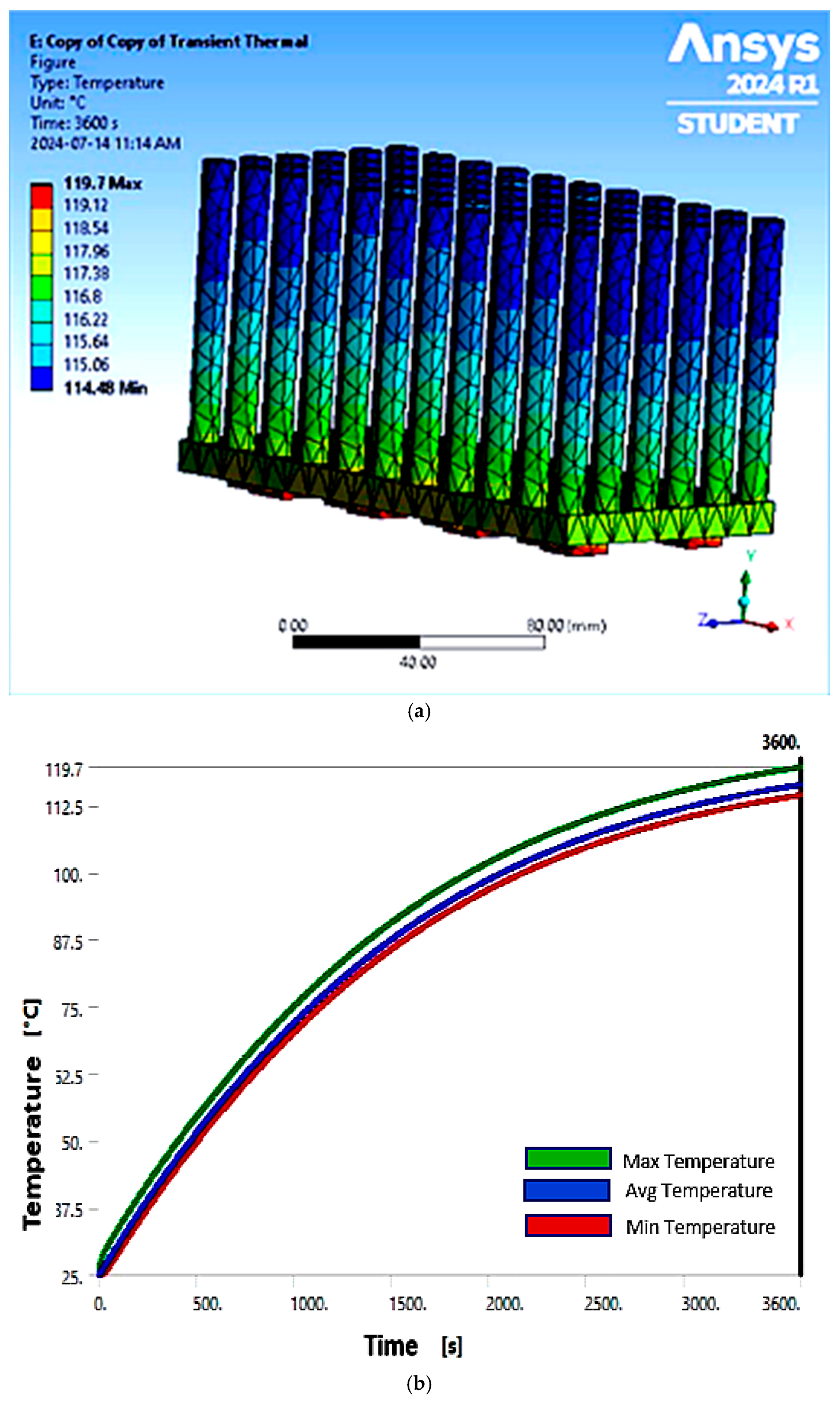
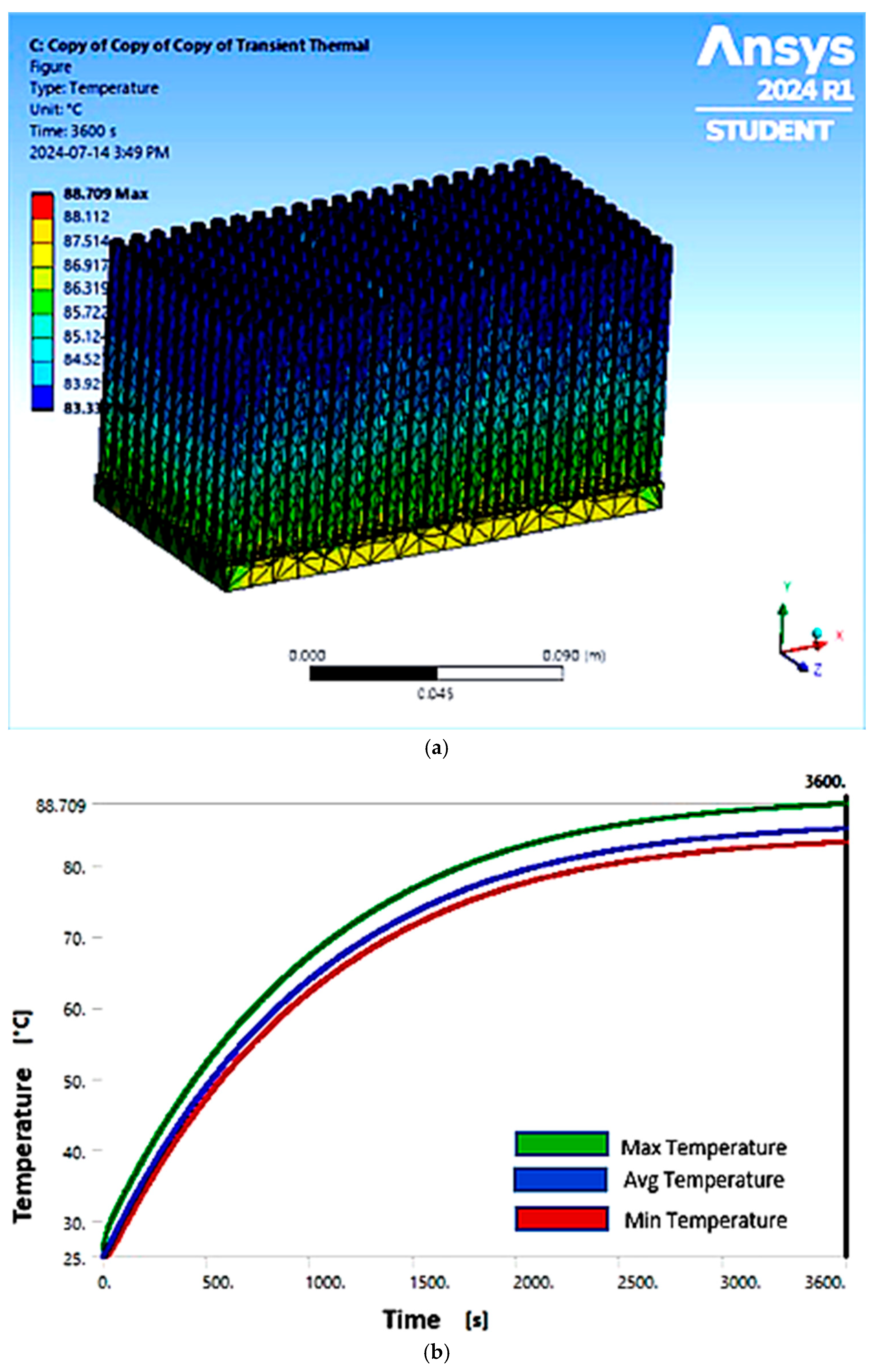
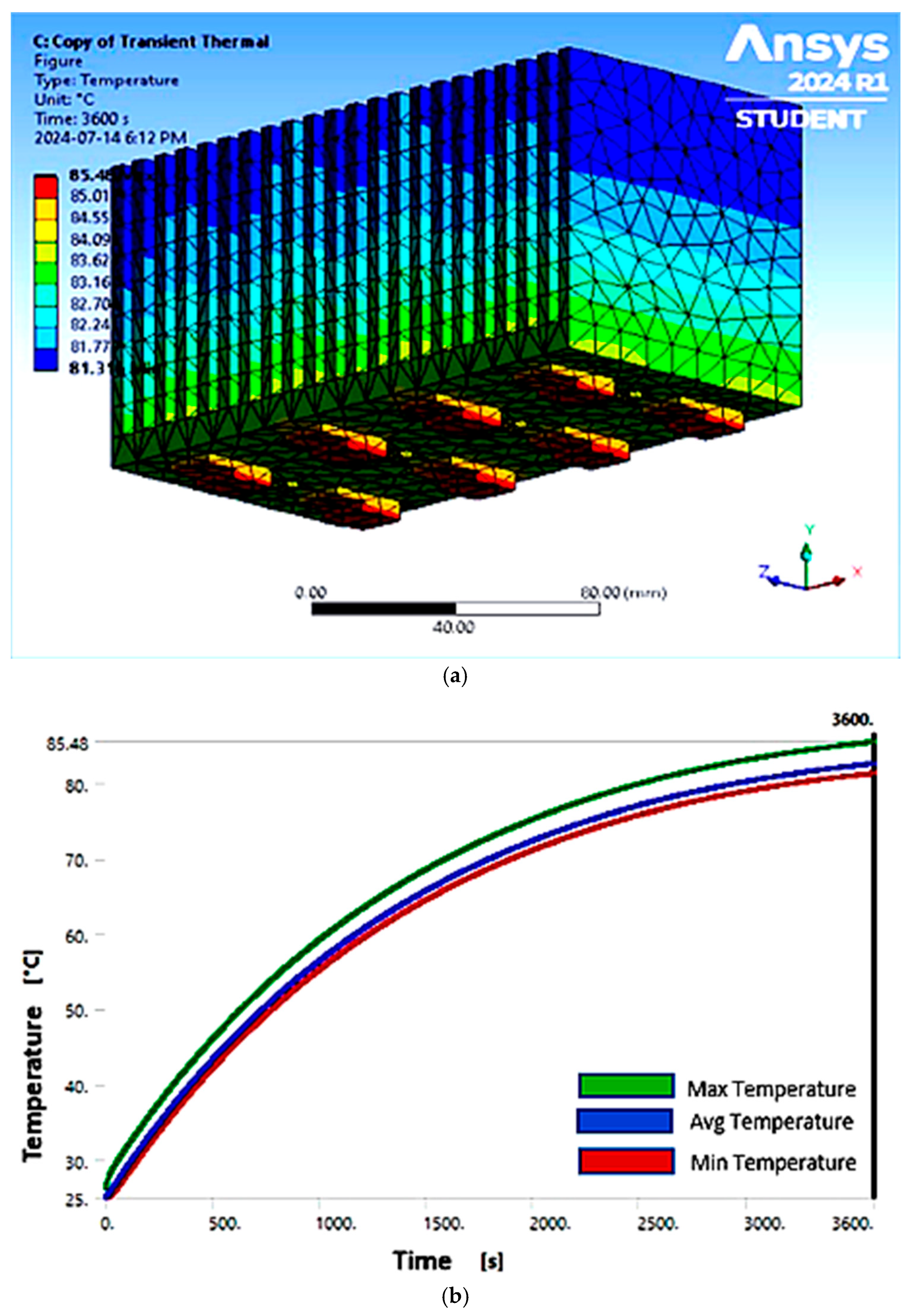
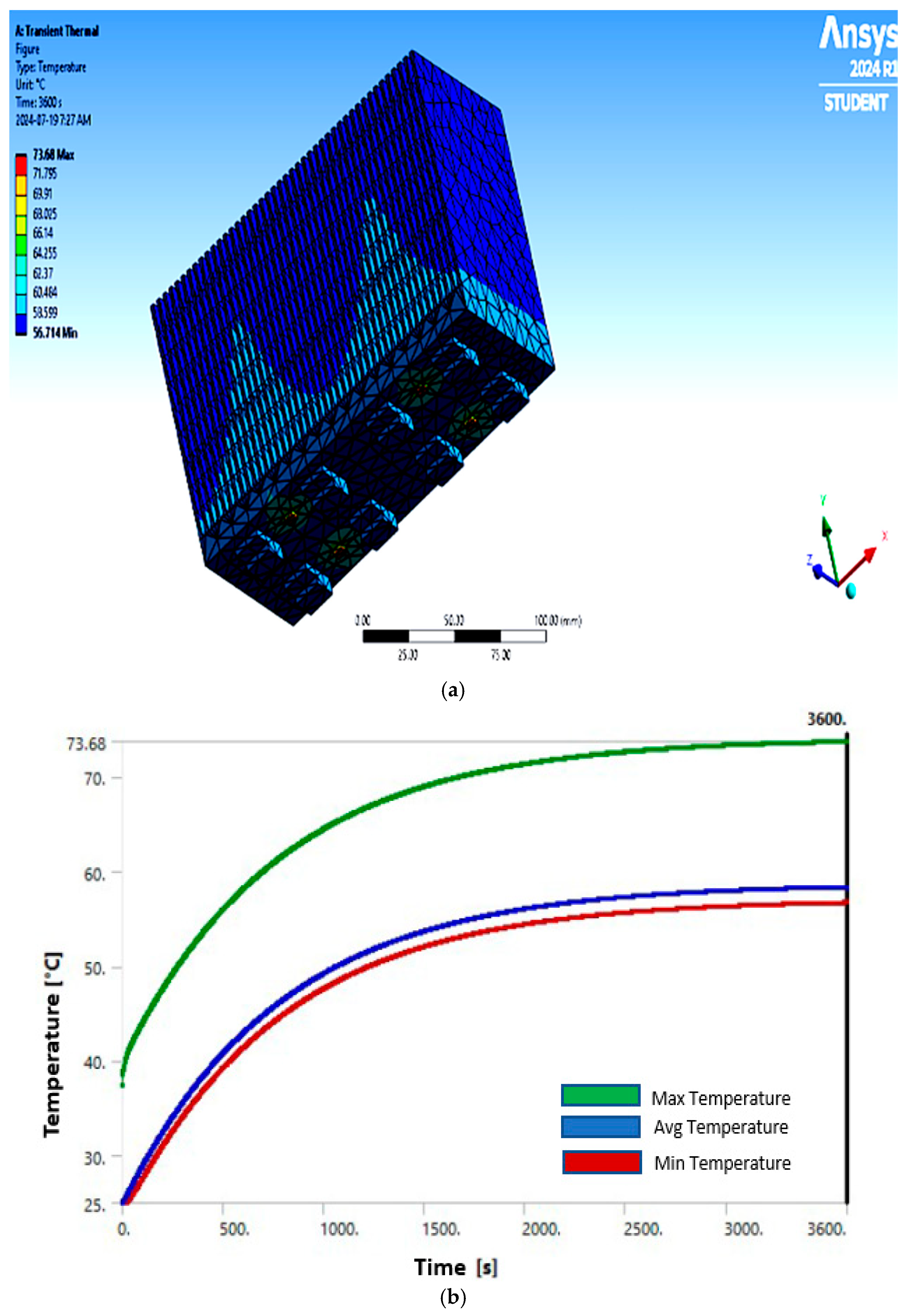
| Max. Temperature (°C) | 119.70 | 88.71 | 73.68 | 85.48 |
| Avg. Temperature (°C) | 116.48 | 85.13 | 66.14 | 83.16 |
| Min. Temperature (°C) | 114.48 | 83.33 | 56.71 | 81.36 |
| Max. Heat Flux (W/m2) | 38,926 | 41,284 | 40,344 | 39,782 |
| Min. Heat Flux (W/m2) | 17,579 | 21,964 | 12,337 | 21,796 |
| Device Tag | S1 | S2 | S3 | S4 | S5 | S6 | S7 | S8 | D1 | D2 | D3 | D4 |
|---|---|---|---|---|---|---|---|---|---|---|---|---|
| Max. Temperature (°C) | 66.14 | 66.08 | 65.82 | 65.89 | 66.04 | 65.94 | 65.82 | 66.11 | 73.67 | 73.68 | 73.679 | 73.68 |
| Device Tag | S1 | S2 | S3 | S4 | S5 | S6 | S7 | S8 | D1 | D2 | D3 | D4 |
|---|---|---|---|---|---|---|---|---|---|---|---|---|
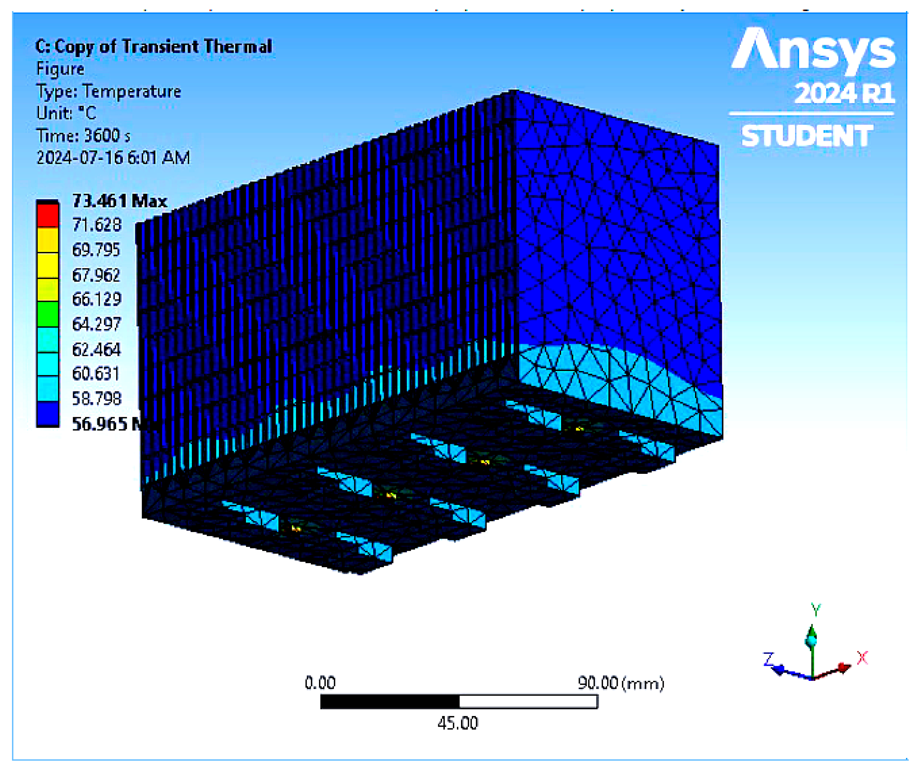
| Max. Temperature (°C) | 59.56 | 59.61 | 59.61 | 59.55 | 59.83 | 59.91 | 59.90 | 59.83 | 73.25 | 73.42 | 73.461 | 73.25 |
| Device Tag | S1 | S2 | S3 | S4 | S5 | S6 | S7 | S8 | D1 | D2 | D3 | D4 |
|---|---|---|---|---|---|---|---|---|---|---|---|---|
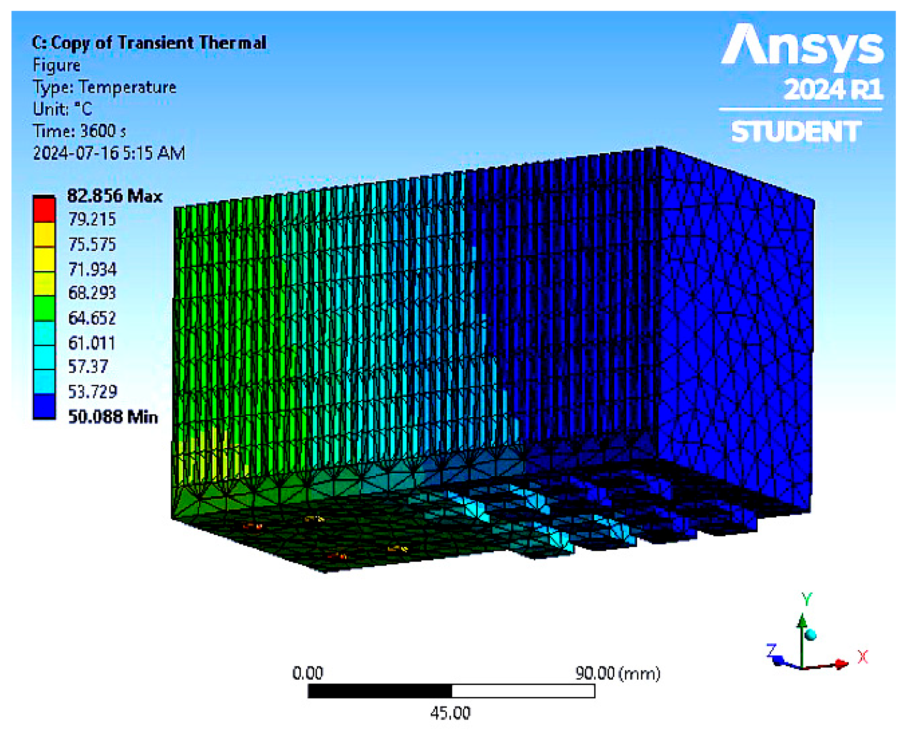
| Max. Temperature (°C) | 52.637 | 53.84 | 55.709 | 58.31 | 52.628 | 53.823 | 55.7 | 58.3 | 80.441 | 82.856 | 80.203 | 82.765 |
| Device Tag | S1 | S2 | S3 | S4 | S5 | S6 | S7 | S8 | D1 | D2 | D3 | D4 |
|---|---|---|---|---|---|---|---|---|---|---|---|---|
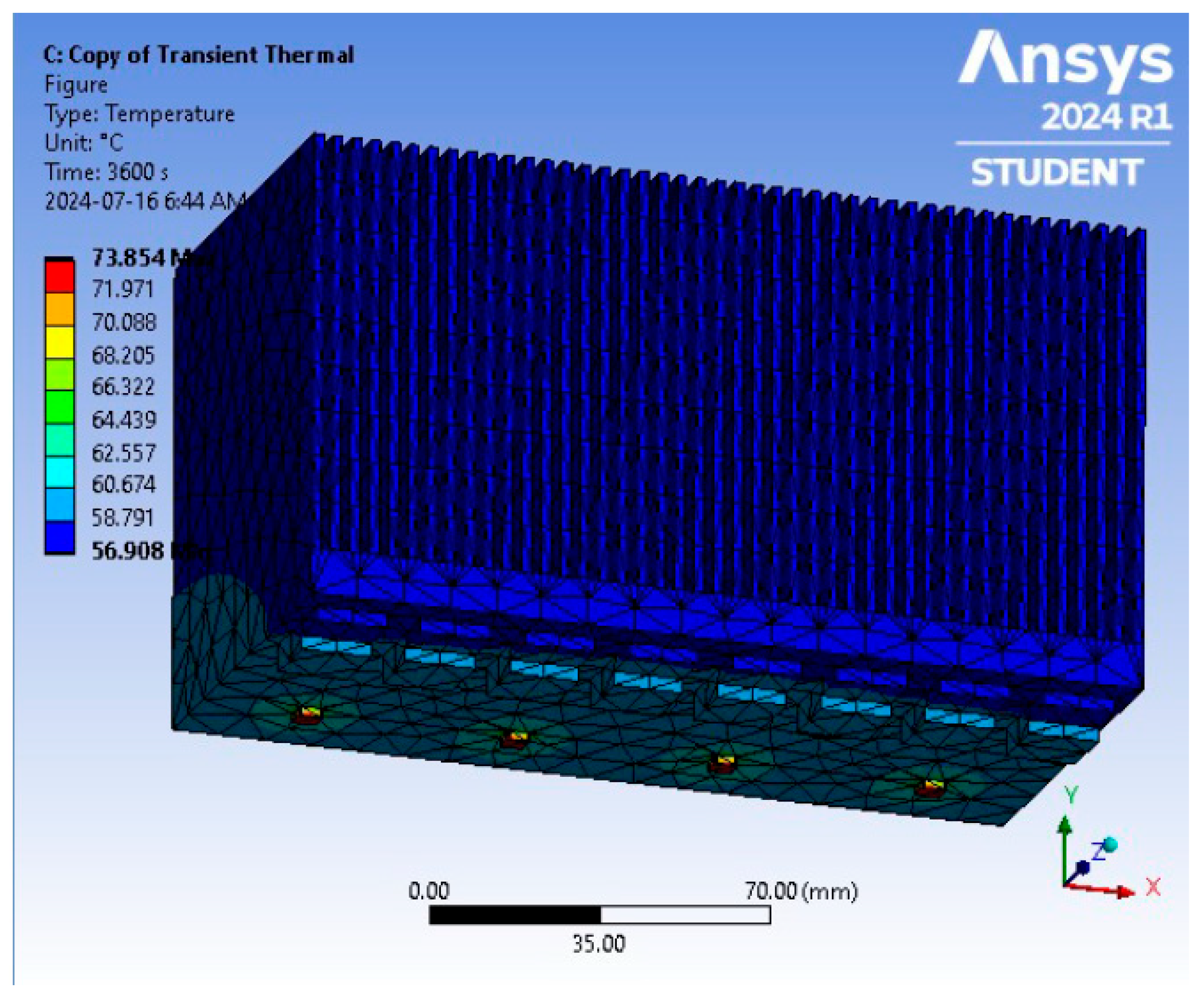
| Max. Temperature (°C) | 58.942 | 58.981 | 59.007 | 59.02 | 59.019 | 59.007 | 58.978 | 58.943 | 73.848 | 73.842 | 73.854 | 73.708 |
| Device Tag | S1 | S2 | S3 | S4 | S5 | S6 | S7 | S8 | D1 | D2 | D3 | D4 |
|---|---|---|---|---|---|---|---|---|---|---|---|---|
| Max. Temperature (°C) | 56.873 | 56.828 | 56.513 | 56.514 | 56.819 | 56.777 | 56.41 | 56.255 | 70.606 | 70.44 | 70.054 | 70.838 |
| Proximity | 100 mm | 200 mm | 300 mm |
|---|---|---|---|
| Maximum Temperatures (°C) | |||
| S1 | 33.735 | 33.735 | 33.733 |
| S2 | 33.909 | 33.91 | 33.909 |
| S3 | 34.355 | 34.356 | 34.355 |
| S4 | 34.379 | 34.38 | 34.38 |
| S5 | 34.015 | 34.015 | 34.015 |
| S6 | 34.021 | 34.019 | 34.018 |
| S7 | 34.414 | 34.413 | 34.412 |
| S8 | 34.469 | 34.469 | 34.469 |
| D1 | 52.505 | 53.172 | 52.488 |
| D2 | 53.177 | 53.176 | 53.175 |
| D3 | 52.476 | 52.459 | 52.467 |
| D4 | 53.187 | 53.180 | 53.171 |
| Heatsink | 40.463 | 40.462 | 40.456 |
| Domain Wall | 42.425 | 49.989 | 41.71 |
| Outlet | 27.294 | 27.266 | 27.241 |
| Variants | P2-D | P2-Di | P2-Dj | P2-Dk | P2-Dl |
|---|---|---|---|---|---|
| Fin Spacing (mm) | 2.14 | 3.65 | 6.48 | 15.8 | 33.6 |
| Maximum Temperatures (°C) | |||||
| S1 | 33.733 | 72.741 | 38.946 | 44.715 | 106.046 |
| S2 | 33.909 | 73.075 | 39.213 | 45.094 | 106.676 |
| S3 | 34.355 | 73.617 | 39.756 | 45.76 | 107.66 |
| S4 | 34.38 | 73.663 | 39.797 | 45.85 | 107.777 |
| S5 | 34.015 | 73.265 | 39.408 | 45.432 | 107.453 |
| S6 | 34.018 | 73.173 | 39.394 | 45.406 | 107.344 |
| S7 | 34.412 | 73.452 | 39.812 | 45.839 | 107.464 |
| S8 | 34.469 | 73.382 | 39.867 | 45.816 | 107.281 |
| D1 | 52.488 | 91.445 | 60.785 | 60.739 | 125.538 |
| D2 | 53.175 | 91.462 | 58.738 | 57.962 | 126.379 |
| D3 | 52.467 | 92.411 | 57.987 | 59.408 | 127.314 |
| D4 | 53.171 | 92.341 | 59.306 | 59.898 | 126.555 |
| Heatsink | 40.456 | 79.814 | 46.174 | 54.644 | 114.38 |
| Domain Wall | 41.71 | 75.894 | 46.666 | 50.77 | 112.263 |
| Outlet | 27.241 | 42.751 | 29.451 | 31.45 | 41.158 |
| Variant | Fin Count | Mass (kg) | Aluminum Material Cost ($C) | Temperature °C | °C/$C |
|---|---|---|---|---|---|
| P2-D | 44 | 2.379 | 6.1854 | 53.171 | 8.596 |
| P2-Di | 33 | 1.894 | 4.9244 | 79.814 | 16.208 |
| P2-Dj | 22 | 1.410 | 3.666 | 46.174 | 12.595 |
| P2-Dk | 11 | 0.925 | 2.405 | 54.644 | 22.721 |
| P2-Dl | 6 | 0.705 | 1.833 | 114.380 | 62.40 |
Disclaimer/Publisher’s Note: The statements, opinions and data contained in all publications are solely those of the individual author(s) and contributor(s) and not of MDPI and/or the editor(s). MDPI and/or the editor(s) disclaim responsibility for any injury to people or property resulting from any ideas, methods, instructions or products referred to in the content. |
© 2025 by the authors. Licensee MDPI, Basel, Switzerland. This article is an open access article distributed under the terms and conditions of the Creative Commons Attribution (CC BY) license (https://creativecommons.org/licenses/by/4.0/).
Share and Cite
Ebere, I.E.; Khan, A.A.; Ogundahunsi, S.; Ugwuemeaju, E.; Khan, U.A.; Ahmed, S. Design and Optimization of the Heatsink of a Level 1 Electric Vehicle Charger. Energies 2025, 18, 180. https://doi.org/10.3390/en18010180
Ebere IE, Khan AA, Ogundahunsi S, Ugwuemeaju E, Khan UA, Ahmed S. Design and Optimization of the Heatsink of a Level 1 Electric Vehicle Charger. Energies. 2025; 18(1):180. https://doi.org/10.3390/en18010180
Chicago/Turabian StyleEbere, Iheanyi Emmanuel, Ashraf Ali Khan, Samuel Ogundahunsi, Emeka Ugwuemeaju, Usman Ali Khan, and Shehab Ahmed. 2025. "Design and Optimization of the Heatsink of a Level 1 Electric Vehicle Charger" Energies 18, no. 1: 180. https://doi.org/10.3390/en18010180
APA StyleEbere, I. E., Khan, A. A., Ogundahunsi, S., Ugwuemeaju, E., Khan, U. A., & Ahmed, S. (2025). Design and Optimization of the Heatsink of a Level 1 Electric Vehicle Charger. Energies, 18(1), 180. https://doi.org/10.3390/en18010180