Article

Study on Surface Charge Inversion and Accumulation Characteristics of DC Pillar Insulators Based on B-Spline Basis Functions

Anhui Province Key Laboratory of Renewable Energy Utilization and Energy Saving, Hefei University of Technology, Hefei 230009, China
*
Author to whom correspondence should be addressed.
Energies 2025, 18(20), 5531; https://doi.org/10.3390/en18205531
Submission received: 7 September 2025 / Revised: 30 September 2025 / Accepted: 14 October 2025 / Published: 21 October 2025

Abstract

Surface charge accumulation is an important cause of flashover accidents for DC pillar insulators and the failure of DC gas insulation equipment. In this paper, the DC pillar insulator is taken as the research object, and a surface potential measurement system is built. The surface potential distribution of the pillar insulator under different voltages is measured. An inversion algorithm based on the B-spline basis function is proposed. The electric field simulation model of the DC pillar insulator considering the gas’s weak ionization and surface conductance is established. The surface charge accumulation characteristics of the pillar insulator under different DC voltages are studied. The results show that the surface potential of the DC pillar insulator presents an oscillating distribution in the axial direction, and the potential distribution is approximately mirror symmetry under positive and negative voltages. The surface charge density is non-uniform in the axial direction, and the surface charge distribution is different under different voltages. In addition, the current density on the solid side gradually approaches and exceeds the current density on the gas side with the increase in the applied voltage, which promotes the accumulation of charges on the insulator surface with the same symbol as the electrode to weaken the field strength and balance the normal electric field components on both sides.

1. Introduction

High-voltage direct current (HVDC) transmission technology has become an important means to optimize energy allocation due to its advantages of large capacity, long distance transmission, and convenient networking [1,2]. Gas-insulated equipment has been widely used in the field of transmission because of its space-saving ability, high reliability, and strong environmental adaptability [3]. AC gas-insulated equipment has made remarkable progress in technology research and engineering applications, and has accumulated rich practical experience. In contrast, the development of DC gas-insulated equipment is relatively slow, and its popularization and application are restricted by many factors, in particular, the accumulation of surface charge on the insulating medium under the action of DC voltage [4,5,6].
Under the condition of high-voltage direct current, the insulator is in a unipolar electric field for a long time, and the charge migrates directionally under the action of electric field force. At the same time, because the gas insulation equipment adopts a sealed structure and maintains a dry environment inside, the surface lacks an effective charge dissipation path, resulting in a large amount of charge on the surface of the insulator. This will not only lead to abnormal electric field distribution, but also may provide sufficient free charge for arc discharge, which poses a serious risk to the safe operation of the equipment [7,8,9]. As a critical component responsible for supporting and securing current-carrying conductors in gas-insulated equipment, research into the surface charge and electric field distribution characteristics of pillar insulators is of paramount importance for investigating the flashover mechanisms at gas–solid insulation interfaces and enhancing DC insulation performance [10,11,12].
In recent years, the surface charge accumulation characteristics of insulators under DC voltage have received extensive attention from academia. Wang Qiang et al. studied the phenomenon of surface charge accumulation on conical insulators, discussed the mechanism of charge accumulation, and pointed out that surface conduction and volume conduction do not seem to dominate the charge accumulation on insulators, and partial discharge in gas may be the main source of the surface charge [13]. Qi Bo et al. studied the surface charge distribution characteristics of basin insulators under DC and AC voltages, and pointed out that the surface charge showed an obvious polarity effect under DC voltage, and the charge accumulated on the surface under AC voltage was negative charge [14]. In the aspect of surface charge inversion algorithms, Ootera et al. studied the spatial distribution characteristics of insulator surface charge accumulation, and used the surface apparent charge method for charge inversion calculation. The algorithm divides the insulator into N regions, and the relationship between surface potential and surface charge is expressed by a transfer matrix. However, with the increase in observation points, the matrix calculation amount of the algorithm also increases significantly [15]. The two-dimensional Fourier inversion technology developed by Kumada′s team has advantages in spatial resolution, but its application is limited by the translation invariance requirements of the system, and it is difficult to accurately measure insulators with thickness changes [16]. Based on the relationship between the surface charge density distribution and the output potential of the electrostatic probe, Wang Han et al. proposed an improved inversion algorithm for calculating the surface charge density and electric field distribution according to the output potential distribution. The algorithm considers the influence of the electrostatic probe on the measurement process and is mainly suitable for the translation invariant system [17].
The research on the characteristics of surface charge accumulation under DC voltage is mostly based on experiments. Due to the increase in observation points, some inversion algorithms used in the existing research often involve the operation of large matrices. This kind of calculation process has significant ill-posed characteristics, that is, a small disturbance in the conversion matrix or the potential distribution matrix will cause a significant deviation in the calculation results, resulting in a misunderstanding of the surface charge accumulation mechanism of the insulating medium. There are still other limitations as well. Therefore, in this paper, an experimental measurement system for the surface potential distribution of pillar insulators in gas-insulated equipment was built, and the surface potential distribution data of insulators under different voltage polarities and amplitudes were obtained. The inversion algorithm based on the B-spline basis function was used to realize the conversion from surface potential to surface charge density. At the same time, the gas–solid composite insulation structure model was established by COMSOL 6.0 software, and the surface charge accumulation process was simulated and analyzed. Combined with the experimental and simulation results, the electric field distribution characteristics and surface charge accumulation mechanism of pillar insulators under DC voltage were discussed in depth.

2. Experimental Platform and Method

2.1. Surface Potential Measurement System

In order to explore the accumulation characteristics of the surface charge of the pillar insulator, a micro insulator sample with a diameter of 40 mm and a height of 90 mm was designed and prepared, and a surface potential measurement system was built. The surface potential distribution at different voltage levels was obtained by measurement, and the initial potential data were provided for the surface charge inversion method.
The surface potential measurement system is shown in Figure 1. The DC voltage output by the high-voltage DC power supply is introduced into the tank through the insulating sleeve. The sample is placed in a closed metal tank with an inner diameter of 0.5 m and a height of 1 m. The upper end is reliably electrically connected to the inner core of the casing through an aluminum guide pole, and the lower end is installed on a 360-degree rotating platform at the bottom of the tank. Potential measurements were performed using a TREK-341B electrostatic potential meter manufactured by TREK Corporation (Waterloo, WI, USA). The probe is fixed on the upper bracket of the servo electric cylinder. By controlling the servo motor and the servo electric cylinder, the rotation of the sample and the up and down movement of the measuring probe can be realized, so as to complete the potential measurement on the surface of the sample. The metal pipe and gas cylinder outside the tank are connected with the vacuum pump. By controlling the inlet switch valve and outlet switch valve on the pipe, the inside of the tank can be inflated or pumped to meet the requirements of the sample measurement in different atmospheres.

2.2. Experimental Method

The experiment is conducted at a constant temperature of 20 °C. First, the surface of the sample is cleaned with anhydrous ethanol, and then dried in a constant temperature oven for 12 h. After the charge is eliminated, the upper electrode is connected with the aluminum rod and extended into the casing to ensure full contact with the casing core, and the lower electrode is fixed on the rotatable base in the tank to complete the sample installation. An appropriate amount of desiccant is placed in the experimental tank to control the ambient humidity inside the tank at a low level.
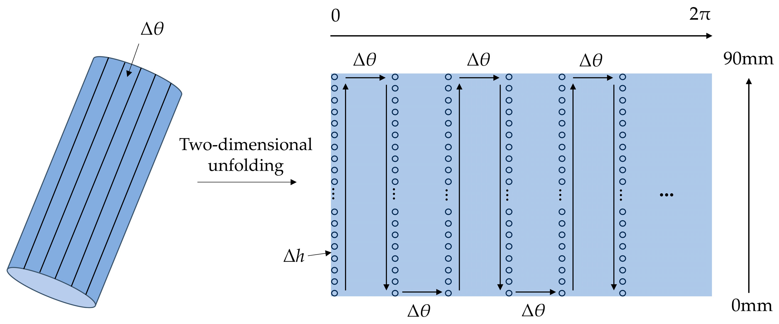
After the experimental preparation is completed, the vacuum pump is started to vacuum the inside of the tank to below 60 Pa, and then the vacuum pump is closed and filled with SF6 gas to 0.5 MPa. The specified voltage is applied by the signal generator and the high-voltage power amplifier, and the voltage is reduced to zero after 2 h of pressurization. The voltage source is turned off, and the surface potential distribution of the insulator sample is detected by the electrostatic potentiometer and the electric rotating platform. Because the measuring probe and the electrode need to maintain a safe insulation distance, the longitudinal measurement range of the system is limited, and the actual effective measurement height is 70 mm. During the measurement process, the surface of the sample is scanned point by point at a circumferential interval of 10° and an axial interval of 1 mm. The surface scanning path of the pillar insulator model is shown in Figure 2. The scanned data are transmitted to the computer through the data acquisition card for storage.

3. Charge Inversion Method Based on B-Spline Basis Function

3.1. Principle of Surface Charge Inversion

As a non-contact measurement technology, the working principle of the electrostatic probe method is based on the electrostatic induction and capacitance coupling mechanism. This method realizes the measurement through the capacitive coupling system composed of the probe and the charged surface: when the probe is close to the charged surface, the surface charge will generate an induced potential inside the probe, and the potential value has a certain quantitative relationship with the surface charge density. The relationship between the probe output potential φ and the surface charge density σ can be expressed as follows:
j = M × s
where M is the scale coefficient, which is related to the geometric parameters of the probe and the measurement distance.
The model assumes that the probe output potential has a simple linear relationship with the surface charge density, and it is difficult to accurately reflect the real charge distribution. The influence of the charge distribution around the measurement point on the probe output potential should be considered. The output potential of the probe actually reflects the superposition effect of all discrete charges in the detection area. In order to establish a mathematical model, the measurement surface is discretized into N finite elements, each of which can be regarded as a point charge source. Based on the superposition principle, the potential and charge density of the i-th measurement point satisfy the following conditions:
φ ( i ) = j = 1 N h ( i , j ) σ ( i )
where h(i,j) is the transfer function, which represents the potential contribution coefficient of the unit charge density at j position to the i-th measurement point.
In order to realize the high-precision reconstruction of the surface charge distribution, the number of measured points N needs to be multiplied, resulting in a sharp expansion of the transfer matrix dimension. However, the inverse operation of a large-dimensional matrix can easily cause ill-conditioned problems, which makes the charge calculation results produce large errors. In order to better solve the above problems, this paper proposes a surface charge inversion method based on the B-spline basis function. Because the surface potential of the pillar insulator decays slowly in the gas environment of 0.5 MPa SF6, and the surface potential measurement time is short, the transient measurement value can be equivalent to the quasi-static potential distribution at the end of pressurization. Ignoring the space charge accumulation effect inside the medium and in the gas environment, the surface potential of the sample can be simplified into a quasi-electrostatic field model. According to the linear superposition principle, the following can be obtained:
φ m × 1 = A m × n k n × 1
φ i = φ r i
A i j = f j r 4 π ε 0 r r i 2   d S
σ ( r ) = j = 1 n k j f j r
where [φ] is the surface potential distribution, [A] is the response matrix, [k] is the coefficient matrix, m is the number of observation points, n is the number of basis functions, φi represents the measured potential at ri on the surface of the pillar insulator, Aij represents the potential at ri on the surface of the pillar insulator when the surface charge distribution is the basis function fj, kj denotes the coefficient of the basis function fj when the surface charge distribution is represented by the basis function group {f1,...,fn}, fj(r) is the basis function for discrete surface charge distribution, and σ(r) is the charge density at point r on the surface of the pillar insulator.
The basis function set for the discrete surface charge distribution is generated by the Cox–de Boor recursive formula, which satisfies the smooth continuity condition and is expressed as follows:
f 12 ( k 1 ) + l r = N 3 , k z z max N 3 , l θ 2 π k 1 , , 30 , l 1 , , 12
where z is the axial coordinate. On the surface of the sample, the minimum axial coordinate is 0, and the maximum axial coordinate is zmax. θ is the circumferential angle, N3,k(·) is a third-order quasi-uniform B-spline basis function, and N3,l(·) is a third-order cyclic B-spline basis function.
The waveforms of quasi-uniform B-spline basis functions and cyclic B-spline basis functions are shown in Figure 3. Based on the properties of third-order B-spline basis functions, N3,k(·) and N3,l(·) are piecewise cubic spline functions. The core advantages of the B-spline basis function lie in its local support, high-order continuity, and flexible order control, which enables it to achieve local shape adjustment through piecewise polynomials, while ensuring smooth curves and effectively avoiding the numerical oscillation of high-order interpolation.

3.2. The Calculation Process of Surface Charge Inversion

On the surface to be measured, m observation points were evenly selected in this study, and these observation points were evenly distributed in the circumferential and axial coordinates. Specifically, the circumferential spacing is set to 10°, and the axial direction is divided into 90 equal parts to ensure that the measurement points fully cover the surface to be measured. At the same time, the simulation model of the pillar insulator is established by COMSOL Multiphysics software, and the charge distribution on the surface of the simulation model is set as the basis function fj(r). The surface potential distribution when the surface charge is each basis function is obtained by simulation calculation, and some simulation results are shown in Figure 4. Based on these simulation results, the potential Aij of each observation point under zero-input response can be further extracted, and the response matrix [A] can be obtained by combining the zero-input response potentials corresponding to all basis functions.
Since the pillar insulator model has an axisymmetric structure, the response matrix [A] exhibits the characteristics of a block circulant matrix. This feature makes the response of the basis function f12(k−1)+l(r) able to be calculated by the response of the basis function fj(r), and the actual simulation times can be reduced from 360 times to 30 times, which significantly reduces the workload of the simulation calculation and greatly improves the calculation efficiency. After obtaining the response matrix [A], it is substituted into the overdetermined linear Equation (3) with the experimentally measured potential distribution [φ] to solve the coefficient matrix [k]. Finally, the inverse charge distribution can be obtained by substituting the solved coefficient matrix into the expression (6) of the surface charge distribution.

3.3. Verification of Inversion Calculation Method

After the inversion distribution is determined by the above method, its accuracy needs to be verified. In the COMSOL model, the surface charge distribution of the pillar insulator model is sin(10πz/zmax)cos(3θ), and the potential distribution of the insulator surface is obtained by simulation. The potential distribution obtained by the simulation is extracted by MATLAB R2022b software, and the response matrix [A] is obtained by combining the zero-input response potential under each basis function. The coefficient matrix [k] is solved to obtain the calculated surface charge distribution. The simulation results of artificially setting the charge and its potential and the surface charge distribution calculated by inversion are shown in Figure 5.
From the above diagram, it can be found that whether using the charge peak position or the charge density at each position, it can be found that whether it is the charge peak position or the charge density at each position, the surface charge distribution obtained by the inversion calculation is more consistent with the surface charge distribution that is considered to be set. The difference between the density peak value is 0.02 C/m2, and the error is 2%. The inversion results show smooth continuity in the circumferential and axial directions, and there is no common numerical oscillation or edge distortion phenomenon in the traditional matrix inversion method, which proves the reliability of the proposed inversion calculation method. At the same time, in order to further evaluate the accuracy of the algorithm, the mean square error peak (PMSE) is introduced as a quantitative index. The calculation formula is as follows:
PMSE = i = 1 N ( σ i σ i ) 2 / ( N A 2 )
where σi is the preset surface charge density, σi is the charge density distribution calculated by the inversion algorithm, A is the maximum value after taking the absolute value, and N is the number of sampling points.
Substituting the artificially set charge distribution into the inversion algorithm, the mean square error peak calculated using the above equation based on the B-spline basis function inversion algorithm is 1.05%. Compared to the minimum mean square error peak of 2.9% in the algorithm from Reference [16], this significantly improves the accuracy of the inversion calculation.
This paper supplements the comparison of traditional charge inversion algorithms under the same artificially set charge distribution. The traditional method performs inversion calculations by dividing the insulator surface grid and setting the unit charge density [13]. Different cell divisions and their traditional inversion calculation results are shown in Figure 6. When the grid density is increased to improve the inversion accuracy, the matrix will be close to the singular value, which makes the calculation result inaccurate. As shown in Figure 6a, when the surface is divided into 3240 cells, the surface charge density is as high as 5.47 C/m2, and the calculation has obvious errors. Although reducing the number of grids can ensure the stability of matrix calculation, it will reduce the inversion accuracy. As shown in Figure 6b, the surface density peak is 0.83 C/m2, and the error is much higher than that based on the B-spline basis function inversion algorithm. At the same time, the traditional method has a sudden change in the charge density value at the edge of the cell, resulting in poor smooth continuity of the inversion. It can be seen that the traditional inversion method has certain limitations when the surface charge distribution of the insulator is more complex.

4. DC Field Calculation Method Based on Charge Accumulation

The DC field simulation model of the pillar insulator with a better physical mechanism should include three key components: the volume conduction equation describing the charge transport inside the insulating material, the gas-side conduction equation characterizing the charge transfer at the gas–solid interface, and the surface conduction equation reflecting the charge transfer along the dielectric surface [18,19].
The early research results show that the change in gas current density and field strength similar to Ohm’s law only exists at a very small field strength. Then the current density will reach saturation and remain unchanged within a certain range of field strength. Only when the field strength exceeds a certain limit will the gas molecules be further ionized under the action of a strong electric field, and the current density will rise again with the increase in field strength, as shown in Figure 7.
The applied voltage of the simulation model established in this paper is in the range of 1~30 kV. The calculation results of the electric field show that the field strength in the remaining areas of the experimental cavity has exceeded the critical value required for the saturation of the gas current density except at the bottom corner, and has not reached the field strength value at which the gas can form a current. At this time, the ions are generated by natural radiation [20]. In the gas domain, positive and negative ions migrate along the power line under the action of the electric field Coulomb force. One part of them recombines to form molecules during the movement, while the other part eventually reaches the electrode surface. The movement of the ions arriving at the electrode surface in the gas gap forms the current in the weakly ionized gas. Therefore, a weakly ionized simulation model is established to describe the gas-side conduction.

4.1. Solid Side Conductance Equation

The internal insulation material satisfies the Gauss theorem and the current continuity equation, and the relationship between the insulator body charge density ρv and the insulator-side current density J1 can be obtained as follows:
( ε 1 φ 1 ) = ρ V
ρ V t + J 1 = 0
where ε1 is the dielectric constant of the insulator medium.
In the case of low field strength inside the insulating medium, the current density J1 and the field strength E1 satisfy Ohm’s theorem [21]:
J 1 = γ 1 E 1 = γ 1 φ 1
where γ1 is the volume conductivity of the insulator dielectric.
Combining (9)–(11), a transient equation about the charge density ρv of the insulator can be obtained as follows:
ρ V t + γ 1 ε 1 ρ V γ 1 2 ε 1 E 1 ε 1 γ 1 = 0
In the gas-insulated metal-enclosed equipment, the temperature distribution of the insulator may be uneven due to the heating of the central conductor. This temperature gradient will cause the dielectric properties of the insulating material to change. The dielectric constant ε1 is less sensitive to temperature changes, and the volume conductivity is greatly affected by temperature. Based on this characteristic, the above formula is simplified, that is, the change in ε1 is ignored, and only the change characteristics of γ1 are considered. The simplified Formula (12) becomes the following:
ρ V t + γ 1 ε 1 ρ V + E 1 γ 1 = 0

4.2. Gas-Side Conductance Equation

In the absence of partial discharge, ions are generated by natural radiation. Since SF6 gas has a strong ability to adsorb electrons, it is assumed that there are only positive and negative polar carriers in the gas medium, and the charge amount of the carrier is consistent with that of a single electron, and the mass and volume of the carrier are consistent with that of the gas molecule. The process of charge change in the gas medium can be described by ionization, recombination, migration, and diffusion.
t c p + c p μ p E 2 D p c p = S α c p c n t c n + c n μ n E 2 D n c n = S α c p c n
2 φ 2 = e ( c p c n ) ε 2
Among them, the carrier diffusion phenomenon in the gas medium can also be regarded as the electromigration process of the carrier under the action of the chemical potential, so the diffusion rate can be calculated according to the Nernst–Einstein relationship.
D = μ p k B T e
where t is time, cp and cn are the mass concentration of positive and negative ions, μp and μn are the positive and negative ion mobility, E2 is the electric field intensity on the gas side, and Dp and Dn are the diffusion rates of positive and negative ions, respectively. S is the ionization rate of the gas; an average ionization rate in the range from 26 to 55 IP cm−3s−1 was measured in SF6 at 0.5 MPa [22]. α is the ion recombination coefficient, e is the elementary charge, ε2 is the dielectric constant of the gas medium, kB is Boltzmann constant, and T is temperature.
The ion recombination reaction rate in the gas can be calculated by the Langevin principle.
α = e ( c p + c n ) ε 2
The gas migration rate is the speed obtained by the gas carrier through the electric field in the average free time:
μ p = μ n = e τ 2 m 0
where τ is the average free time, and m0 is the molecular weight of gas.
Under the action of the direct current electric field, the charged particles in the gas medium will produce directional migration movement, accompanied by the diffusion effect, and its current density can be expressed as follows:
J 2 = e E 2 ( c p μ p c n μ n ) e ( D p c p D n c n )

4.3. Gas–Solid Interface Charge Density Equation

Based on the current continuity equation, Volpov established a transient theoretical model of surface charge density, which ignores the thickness of the conductive layer in the derivation process [23]:
σ t = J 1 n J 2 n J τ τ
where σ is the surface charge density, and J1n and J2n are the normal components of J1 and J2, respectively. Jτ is the tangential line current source, and n and τ correspond to the unit vectors in the normal and tangential directions of the surface, respectively.
When the surface tangential current Jτ and the surface tangential field strength Eτ satisfy Ohm’s law, the following is obtained:
σ t = J 1 n J 2 n ( χ E τ )
Based on the definition of conductivity and the geometric characteristics of the conductive layer, the following applies:
χ = γ 1 d
where χ is the surface conductivity, and d is the thickness of the conductive layer.

4.4. Boundary Condition Setting

According to the Dirichlet boundary conditions, the potential distributions at the high-voltage electrode and the grounded electrode satisfy the following, respectively:
φ HV = u ( t )
φ GND = 0
where u(t) is the applied voltage of the high-voltage electrode.
For the floating potential electrode, its surface net charge is zero, so it satisfies the following:
S n · E d S = 0
where n is the unit normal vector of the electrode surface; S is the electrode surface integral domain.
Based on COMSOL Multiphysics simulation software, this study established a multi-physical field simulation model of the pillar insulator under the 0.5 MPa SF6 gas environment and temperature of 293.15 K. Specifically, the electric field intensity distribution in the solid medium region is calculated by Electrostatics; the transport process of positive and negative ions and their space charge density distribution in the gas medium are simulated by the Transport of Diluted Species. At the same time, the charge accumulation characteristics at the gas–solid interface are analyzed by Boundary ODEs and DAEs. The specific parameters of the simulation model are shown in Table 1. The multi-physics coupling relationship of the DC field model is shown in Figure 8.

5. Surface Charge Accumulation Characteristics and Mechanism Analysis

5.1. Surface Charge Distribution Characteristics

Using the simulation model established in Section 4, the surface potential and surface charge distribution of the pillar insulator after 2 h of DC voltage are numerically calculated. According to the test data, the relative dielectric constant is set to 6 in the simulation model, the volume conductivity of the insulator is 5 × 10⁻¹⁶ S/m, and the gas diffusion rate is calculated to be 1.2126 × 10⁻⁷ m2/s according to (16). The simulation results are shown in Figure 9 and Figure 10.
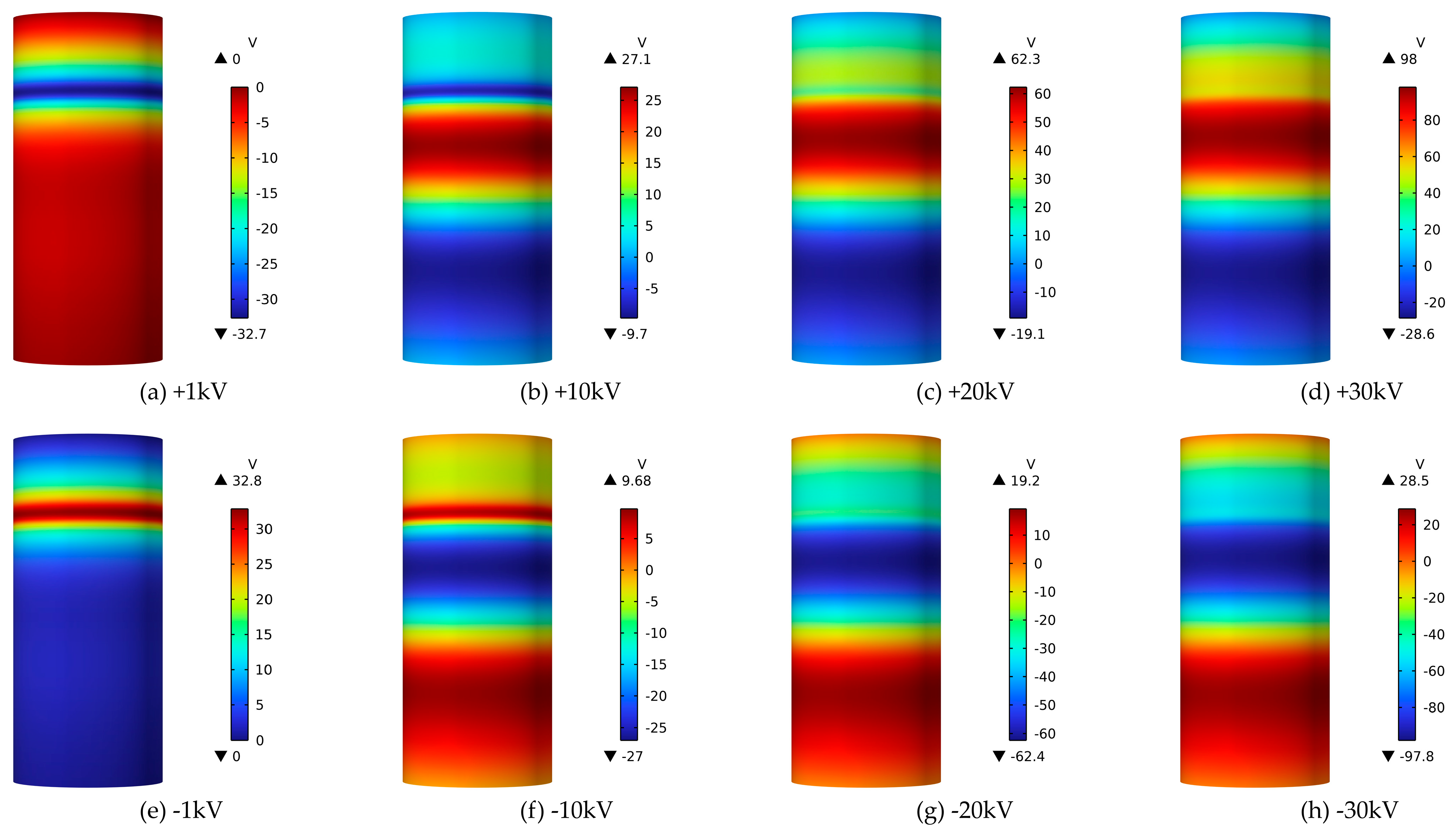
The vertical direction in the figure corresponds to the axial coordinate of 0~90 mm. The simulation results show that the surface potential distribution is basically the same in the ring direction, while it presents an oscillating distribution in the axial direction. It changes dynamically with the increase in voltage, and the overall trend is increasing. The potential distribution under positive and negative voltages is approximately mirror symmetry. The surface charge density almost does not change in the ring direction, but shows significant non-uniformity in the axial direction. Local high-concentration positive and negative charges appear alternately, and there is a spatial correspondence between the charge density extreme area and the potential extreme area, but the charge density peak width is narrow. In addition, the overall trend of the surface charge distribution under different voltages is different.
According to the experimental scheme described in Section 2, a series of voltage loading experiments were carried out on the insulator samples. The test voltages were set to ±1 kV, ±10 kV, ±20 kV, and ±30 kV. After 2 h of continuous pressurization, the surface potential data of the samples were measured by electrostatic probe. The area outside the measurement range was supplemented by simulation data. Based on the potential data, the inversion algorithm based on the B-spline basis function described in Section 3 was used to calculate the surface charge distribution, as shown in Figure 11. The simulation and inversion results are highly consistent in charge distribution trend, peak position, and size.
In order to further analyze the difference in surface potential and charge distribution under different DC voltages, a straight line is selected along the axial direction in the simulation and inversion model, and the potential and charge distributions at different heights are counted. The results are shown in Figure 12. Each measurement data point includes the maximum, minimum, and average values along the sample at the same height, which are presented in the form of an error bar.
With the change in the applied DC voltage, the surface charge distribution of the pillar insulator sample shows a significant spatial evolution law. Under the condition of 1 kV low voltage, the surface charge is mainly heteropolar, and the accumulation peak is concentrated in the upper part of the insulator. The vertical height is about 70 mm, the peak width is narrow, and the full width at half maximum is about 3–5 mm. When the voltage is increased to 10 kV, the heteropolar charge peak in the upper part of the sample remains basically unchanged, while a small amount of homopolar charge accumulation occurs in the middle and upper regions near the axial 60 mm, and a small amount of heteropolar charge accumulation occurs in the lower region of the axial about 30 mm. The boundary height between the two is about 40 mm. As the voltage further increases to 20 kV and 30 kV, the upper heteropolar charge peak gradually weakens, and the middle and upper homopolar charge accumulation is significantly enhanced. At 30 kV, the peak reaches about 0.52 μC/m2, and exceeds the upper part to become the highest peak. At the same time, the charge density at the top area with a height greater than 72 mm and the lower area with a height less than 30 mm increases synchronously, forming a multi-peak coexistence distribution pattern.

5.2. Analysis of Surface Charge Accumulation Mechanism

The spatial evolution of the surface charge distribution of the pillar insulator can be attributed to the coupling effect of the dynamic balance mechanism of the gas–solid interface current density and the field intensity modulation effect. It can be seen from the power line distribution in Figure 13 that most of the power lines emitted from the upper electrode finally pass through the outer side of the lower electrode or the grounding shell after passing through the upper part of the insulator model, and only a small number of power lines with a shorter length pass through the lower part and, finally, the lower insert. Therefore, the current density of the gas side at the lower part of the test sample is small. According to (20), the surface should accumulate the same number of charges to weaken the field strength of the solid side and balance the normal electric field components on both sides. When the current density of the solid side satisfying Ohm’s law increases with the increase in the applied voltage, the accumulation of the same number of charges further increases.
At the same time, Figure 13 shows that the power lines in the upper part of the insulator are denser, and the current density of the gas side at this position is larger, so the surface charge accumulation mode at this position is closely related to the voltage amplitude. Under low-voltage conditions, the gas-side current density near the high-voltage electrode is dominant, while the solid-side current density is at a low level. According to (20), in order to compensate for the difference in current density on both sides of the gas–solid, the charge opposite to the upper electrode symbol preferentially accumulates in the upper region of the insulator, enhances the field strength on the solid side, and forms a single narrow peak distribution with a height of about 70 mm. At this time, the charge mainly comes from the ions generated by natural radiation on the gas side. As the applied voltage increases to 10 kV, the current density on the solid side follows Ohm’s law and increases linearly with the field strength. At this time, the current density on the solid side exceeds the gas side locally at a height of about 60 mm in the middle and upper parts, and the charge with the same symbol as the upper electrode needs to be accumulated to weaken the field strength on the solid side. At the same time, due to the small current density on the gas side, the area below 30 mm near the lower grounding electrode needs to accumulate the same charge as the lower electrode symbol to weaken the local field strength, forming a spatial layered structure with 40 mm as the boundary. As the voltage further increases to 20 kV and 30 kV, the current density on the solid side further increases with the increase in the field strength and exceeds the current density on the gas side, resulting in a gradual decrease in the charge accumulation near 70 mm that is opposite to the symbol of the upper electrode, while the charge accumulation in the middle and upper parts that is the same as the symbol of the upper electrode is significantly enhanced, reaching a peak of about 0.52 μC/m2, becoming the highest peak. At the same time, the charge accumulated in the area below 30 mm also increases with the increase in the applied voltage, and finally forms a multi-peak coexistence distribution pattern.

6. Conclusions

In this study, the influence of different DC voltage amplitudes on the surface charge accumulation of pillar insulators was systematically studied by building a surface potential measurement system, combining the inversion algorithm based on the B-spline basis function and a multi-physics simulation model. The main results are as follows:
(1)
A surface charge inversion method of pillar insulators based on the B-spline basis function is proposed. The inversion shows smooth continuity in the circumferential and axial directions. The density peak error is only 2%, and the mean square error peak is 1.05%. Compared with the traditional inversion algorithm, it has obvious advantages in computational efficiency and accuracy. The charge distribution obtained by the proposed multi-physics coupling simulation model is consistent with the inverted charge distribution from the change trend, the position of the charge peak, and the size of the charge peak.
(2)
The surface potential distribution is basically the same in the ring direction, but it shows an oscillating distribution in the axial direction. It changes dynamically with the increase in voltage, and the overall trend is increasing. The potential distribution under positive and negative voltages is approximately mirror symmetry. The surface charge density almost does not change in the ring direction, but shows significant non-uniformity in the axial direction. The lower part of the sample always accumulates the same charge as the lower electrode symbol. The upper part of the sample accumulates a small amount of charge opposite to the upper electrode symbol when the voltage is 1 kV. With the increase in voltage, the same charge as the upper electrode symbol begins to accumulate. In the amplitude range of 1~30 kV, the charge peak opposite to the upper electrode symbol always exists in the upper part of the sample, and gradually decreases with the increase in voltage.
(3)
The modulation mechanism of the amplitude of the applied voltage on the dynamic balance of the gas–solid interface current and the surface charge accumulation is revealed: the current density on the upper part of the gas side is larger, and the current density on the lower part is smaller. Under low-voltage conditions, the current density on the upper solid side is less than that on the gas side, and the charge on the upper part of the insulator accumulates with the opposite sign of the upper electrode. With the increase in the applied voltage, the current density on the solid side increases, and the charge on the surface of the insulator accumulates with the same sign of the electrode to weaken the field strength and balance the normal electric field components on both sides.

Author Contributions

X.Y.: conceptualization, resources, and writing—original draft; H.X.: software, validation, and data curation; J.W.: methodology and writing—review and editing; J.Z.: funding acquisition and visualization; S.L.: investigation and formal analysis; X.F.: project administration and supervision. All authors have read and agreed to the published version of the manuscript.

Funding

This research was supported by the Fundamental Research Funds for Central Universities (No.PA2024GDSK0072).

Data Availability Statement

The original contributions presented in this study are included in the article. Further inquiries can be directed to the corresponding author.

Conflicts of Interest

The authors declare no conflicts of interest.

References

  1. Tang, H.; Wu, G.; Chen, M.; Deng, J.; Li, X. Analysis and Disposal of Typical Breakdown Failure for Resin Impregnated Paper Bushing in the Valve Side of HVDC Converter Transformer. Energies 2019, 12, 4303. [Google Scholar] [CrossRef]
  2. Muzzammel, R. Traveling Waves-Based Method for Fault Estimation in HVDC Transmission System. Energies 2019, 12, 3614. [Google Scholar] [CrossRef]
  3. Zhu, C.; Duan, X.; Li, S.; Zhang, Z.; Guan, J.; Xin, Y.; Gao, Y. Effect of Gas Content on Surface Charge Accumulation of Epoxy Insulator in C4F7N/CO2/O2 Mixture Under AC Voltage. Energies 2025, 18, 4390. [Google Scholar] [CrossRef]
  4. Moukengué Imano, A. Accumulation of surface charges on the particle contaminated spacer surface in compressed gas under impulse voltage stress. J. Electrostat. 2004, 61, 1–19. [Google Scholar]
  5. Feng, W.; Yuchang, Q.; Pfeiffer, W.; Kuffel, E. Insulator surface charge accumulation under impulse voltage. IEEE Trans. Dielectr. Electr. Insul. 2004, 11, 847–854. [Google Scholar] [CrossRef]
  6. Zhu, F.; Fouracre, R.A.; Fairish, O. Investigations of surface charging of DC insulator spacers. In Proceedings of the 1995 Conference on Electrical Insulation and Dielectric Phenomena, Virginia Beach, VA, USA, 22–25 October 1995; pp. 428–431. [Google Scholar]
  7. Ma, J.; Zhang, Q.; You, H.; Wu, Z.; Wen, T.; Guo, C.; Wang, G.; Gao, C. Study on insulation characteristics of GIS under combined voltage of DC and lightning impulse. IEEE Trans. Dielectr. Electr. Insul. 2017, 24, 893–900. [Google Scholar] [CrossRef]
  8. Du, B.; Huang, P.; Xing, Y. Surface charge and flashover characteristics of fluorinated PP under pulse voltage. IET Sci. Meas. Technol. 2017, 11, 18–24. [Google Scholar] [CrossRef]
  9. Gao, Y.; Zhao, H.; Yuan, X.; Wang, H. Numerical simulation of surface charge inhibition performance on epoxy insulator under DC voltage by flexible coating strategy. High Volt. 2022, 7, 553–563. [Google Scholar] [CrossRef]
  10. Zhu, M.; Wang, L.; Yin, F.; Farzaneh, M.; Mei, H.; Wen, L. The Effect of a Vertical Electric Field on the Surface Flashover Characteristics of a Bushing Model. Energies 2018, 11, 1607. [Google Scholar] [CrossRef]
  11. Xing, Y.; Wang, Z.; Liu, L.; Xu, Y.; Yang, Y.; Liu, S.; Zhou, F.; He, S.; Li, C. Defects and failure types of solid insulation in gas-insulated switchgear: In situ study and case analysis. High Volt. 2022, 7, 158–164. [Google Scholar] [CrossRef]
  12. Ma, J.; Tao, F.; Ma, Y.; Zhao, K.; Li, H.; Wen, T.; Zhang, Q. Quantitative Analysis on the Influence of Surface Charges on Flashover of Insulators in SF6. IEEE Trans. Dielectr. Electr. Insul. 2021, 28, 274–281. [Google Scholar] [CrossRef]
  13. Wang, Q.; Zhang, G.; Wang, X. Characteristics and mechanisms of surface charge accumulation on a cone-type insulator under dc voltage. IEEE Trans. Dielectr. Electr. Insul. 2012, 19, 150–155. [Google Scholar] [CrossRef]
  14. Qi, B.; Gao, C.; Liu, S.; Zhao, L.; Li, C. Surface charge distribution on GIS insulator under DC/AC voltage. IEEE Trans. Dielectr. Electr. Insul. 2017, 24, 3173–3181. [Google Scholar] [CrossRef]
  15. Ootera, H.; Nakanishi, K. Analytical method for evaluating surface charge distribution on a dielectric from capacitive probe measurement-application to a cone-type spacer in +or-500 kV DC-GIS. IEEE Trans. Power Deliv. 1988, 3, 165–172. [Google Scholar] [CrossRef]
  16. Kumada, A.; Okabe, S. Charge distribution measurement on a truncated cone spacer under DC voltage. IEEE Trans. Dielectr. Electr. Insul. 2004, 11, 929–938. [Google Scholar] [CrossRef]
  17. Wang, H.; Xue, J.Y.; Wang, Y.B.; Su, G.Q.; Deng, J.B.; Mu, H.B.; Zhang, G.J. Improved algorithm of surface charge density distribution and electric field distribution on insulating materials. In Proceedings of the 2017 1st International Conference on Electrical Materials and Power Equipment, Xi’an, China, 14–17 May 2017; pp. 332–335. [Google Scholar]
  18. Okabe, S.; Kumada, A. Measurement Methods of Accumulated Electric Charges on Spacer in Gas Insulated Switchgear. IEEE Trans. Power Deliv. 2007, 22, 1547–1556. [Google Scholar] [CrossRef]
  19. Lutz, B.; Kindersberger, J. Surface charge accumulation on cylindrical polymeric model insulators in air: Simulation and measurement. IEEE Trans. Dielectr. Electr. Insul. 2011, 18, 2040–2048. [Google Scholar] [CrossRef]
  20. Schueller, M.; Straumann, U.; Franck, C.M. Role of ion sources for spacer charging in SF6 gas insulated HVDC systems. IEEE Trans. Dielectr. Electr. Insul. 2014, 21, 352–359. [Google Scholar] [CrossRef]
  21. Guillermin, C.; Rain, P.; Rowe, S.W. Transient and steady-state currents in epoxy resin. J. Phys. D Appl. Phys. 2006, 39, 515. [Google Scholar] [CrossRef]
  22. Kindersberger, J.; Lederle, C. Surface charge decay on insulators in air and sulfurhexafluorid—Part I: Simulation. IEEE Trans. Dielectr. Electr. Insul. 2008, 15, 941–948. [Google Scholar] [CrossRef]
  23. Volpov, E. HVDC gas insulated apparatus: Electric field specificity and insulation design concept. IEEE Electr. Insul. Mag. 2002, 18, 7–36. [Google Scholar] [CrossRef]
  24. Straumann, U.; Schuller, M.; Franck, C.M. Theoretical investigation of HVDC disc spacer charging in SF6 gas insulated systems. IEEE Trans. Dielectr. Electr. Insul. 2012, 19, 2196–2205. [Google Scholar] [CrossRef]
  25. Chen, M.; Liu, X.; Liang, C.; Zhao, Y.; Tang, H. Study on Surface Charge Accumulation Characteristics of Resin Impregnated Paper Wall Bushing Core Under Positive DC Voltage. Energies 2019, 12, 4420. [Google Scholar] [CrossRef]
Figure 1. Surface potential measurement system.
Energies 18 05531 g001
Figure 2. Surface scanning path of the pillar insulator model.
Energies 18 05531 g002
Figure 3. Function waveforms: (a) quasi-uniform B-spline basis function; (b) cyclic B-spline basis function.
Energies 18 05531 g003
Figure 4. Simulation results of the basis function f12(k−1)+l(r).
Energies 18 05531 g004
Figure 5. Verification process for charge inversion methods: (a) the manually set charge distribution; (b) the simulated potential distribution; (c) the charge inversion results.
Energies 18 05531 g005
Figure 6. Different cell divisions and their traditional inversion results: (a) 3240 cells; (b) 120 cells.
Energies 18 05531 g006
Figure 7. Relationship between gas current density and field strength.
Energies 18 05531 g007
Figure 8. Multi-physics field coupling relationship for DC field modeling.
Energies 18 05531 g008
Figure 9. Surface potential simulation results of the pillar insulator model.
Energies 18 05531 g009
Figure 10. Surface charge simulation results of pillar insulator model.
Energies 18 05531 g010
Figure 11. Surface charge inversion results of the pillar insulator model.
Energies 18 05531 g011
Figure 12. Surface potential of pillar insulator specimens under different DC voltages: (a) 1 kV, (b) 10 kV, (c) 20 kV, (d) 30 kV; and the corresponding surface charge distributions: (e) 1 kV, (f) 10 kV, (g) 20 kV, (h) 30 kV.
Energies 18 05531 g012
Figure 13. Distribution of power lines on the insulator surface.
Energies 18 05531 g013
Table 1. Simulation model parameters.
NamePhysical QuantityNumerical ValueReference
Formation Rate of Gas Ion PairS/(IP·cm−3·s−1)50[20]
Positive and Negative Ion Mobilityμp, μn/(cm2·V−1·s−1)4.8[20]
Ion Recombination Coefficientα/(cm3·s−1)2.3 × 10−7[24]
Boltzmann’s ConstantkB/(J·K−1)1.38 × 10−23[25]
Relative Dielectric Constant of SF6ε21.002[25]
Disclaimer/Publisher’s Note: The statements, opinions and data contained in all publications are solely those of the individual author(s) and contributor(s) and not of MDPI and/or the editor(s). MDPI and/or the editor(s) disclaim responsibility for any injury to people or property resulting from any ideas, methods, instructions or products referred to in the content.