Abstract
The novel concept of reliable voltage balancing on N fast high-voltage (HV) transistors, connected in series, is verified by computer modeling/experimental testing. The essence of the concept is to transfer the balancing function from conventional snubbers, resistive dividers, varistors, etc., or sophisticated gate-side control techniques, to “individual” resistive loads (of transistors) connected to “individual” HV sources of power. The concept has been implemented in the recently patented architecture of HV rectangular pulse generators. The operation of any series-connected stack requires (1) synchronization of control actions on gates of all N transistors; (2) static HV balancing on all transistors in OFF states; and (3) dynamic HV balancing during ON↔OFF transients. The goals of the new design are to achieve an exceptionally high level of HV balancing in modes (2) and (3), as well as to simplify the process of configuring/customizing the circuit. Testing confirms that new generators exhibit minimal ripple during ON→OFF transients. Reliable operation with high-quality rectangular pulses is ensured even at a voltage slew rate of more than 100 kV/µs, while each transistor blocks a voltage close to the maximum value specified in its datasheet. The presented novelties are likely suitable for high-speed instrumentation.
1. Introduction
High-voltage (HV) rectangular pulse generators with different architectures, designs, circuit topologies, and switch types [1,2,3,4,5] find applications in a wide variety of electronic systems used in scientific experiments, national defense, biomedical treatments, tests, and measurements. Wide-gap semiconductor switches have excellent performance parameters. Silicon carbide (SiC) transistors are superior to their silicon counterparts in a number of aspects [6,7]: electrical breakdown field, thermal conductivity, saturated electron drift velocity, on-resistance, and some others.
For a field-effect transistor (FET), the gate length determines the speed characteristics and the time required for electrons to travel through the gate-driven channel. Therefore, in a comparison of different FETs, it can be expected that the switching speed of HV transistors (different manufacturers [8,9,10,11,12,13,14]) decreases as the maximum blocking voltage (Umax) and on-state current rating increase. Although these trends are possible to visualize through SPICE modeling, it is not always possible to directly compare the switching characteristics using the same computer software. There are many specialized software programs, but some of them model transistors from specific manufacturers, while using SPICE models from external sources can lead to problems and errors.
The highest Umax of commercial SiC transistors is still below 5 kV. Examples include 3.3 kV [12] and 4.7 kV [13]. Identical HV transistors connected in series can provide a combination of high switching speed between OFF and ON states and high blocking voltage (U~N*Umax). In stacks, series-connected transistors also demonstrate (1) a lower drain-to-source resistance in ON state, (2) a higher current density, and (3) are less susceptible to the effects of cosmic radiation compared to a single HV transistor [15]. Stacks have a wide range of applications in the area of power electronics and converter systems. HV rectangular pulse generators belong to the mentioned areas and, in addition, fall into the subclass of high-speed instrumentation [16,17].
For an ideally designed stack, the slew rate of a rectangular HV pulse depends on the speed characteristics of wide-gap HV transistors that become faster and faster over time. Therefore, the design of stacks, reliable, easily, and flexibly adapted to any type of high-speed transistors, is an urgent task.
Real transistors exhibit variations in parameters; this involves well-known technical problems related to voltage imbalance on transistors [3,4,5]. The perfect balance is particularly difficult to achieve in cases of high-quality HV rectangular pulses, as quasi-rectangular waveforms have a large voltage slew rate, dU/dt. When operating in such challenging conditions, the first transistor performing the ON→OFF transition (and the last transistor performing the OFF→ON transition) receives most of the stack voltage; this can cause the transistor to fail.
HV pulse generators exist in two basic configurations: (1) S-L-St-G and (2) S-St-L-G, where St is the stack of N transistors, L is the resistive load, S is the HV source of power, and G is the ground node. Here, we deal with the S-L-St-G configuration, in which the decoupling capacitor eliminates the constant HV on the object of influence [18].
There are many ways to improve the quality of HV equalization (balancing) on series-connected transistors of the same type. The combination of advantages and limitations of particular techniques is analyzed in a number of reviews [1,2,3,4,5,15]. For instance, in the large-scale production of HV pulse generators [18,19], specialized companies may employ pre-selected transistors that are not exactly identical but vary only slightly in terms of parameters. However, this approach to voltage equalization requires a large number of transistors for per-selection. This is one of the current methods for solving the voltage equalization problem.
In sophisticated gate-side methods of voltage equalization [20], high-speed control circuits respond to HV in N×MOSFET and regulate the gates of all transistors. The complexity of setting up the entire system where the stack is in the states with large voltage slew rates on the order of 100 kV/µs limits the use of such feedback.
In practice, common approaches to voltage equalization across transistors of the same type include the use of resistive dividers, varistors, and snubbers to prevent voltage imbalance [3,21,22]. These approaches also have well-known limitations [3,22]. In particular, there is a lack of universality in using specific chains of electronic components that respond to a certain frequency range (for example, the snubber time constant [22]). The efficiency of known dynamic equalization methods decreases with increasing switching speed. The complexity of the problem increases significantly if the stack contains fast transistors of different types.
Some reviews [23,24] describe advanced methods for voltage equalization. We developed a new concept for voltage balancing for stacks with all transistors of different types. Our concept leads to the creation of innovative circuitry for HV pulse generators suited for high-speed instrumentation [25,26]. New generators enabled the pulsed vacuum emission of ions (electrons) from liquid metals [25]. Such generators will find applications in our R&D for advanced superionic conductors and emission nanoionics.
A key feature of the new HV generators is the use of several (N) independent HV sources of power and, correspondingly, N resistive transistor loads (as opposed to one source and one load in traditional designs [3], see Fig. 9 in [17]). These innovations provide reliable, fast, and high-quality voltage balancing in serial-connected transistors.
It is important to differentiate between the term “voltage equalization”, which is appropriate for stacks containing transistors of the same type, and “voltage balancing”, which more accurately describes the technical effect related to the proposed concept. Thanks to the proposed new architecture of HV pulse generators, transistors with similar dynamic characteristics but significantly different Umax can function consistently in a stack. In this context, the term “voltage equalization” refers to one particular case of voltage balancing.
The modern various SPICE software allow one to clearly prove the correctness, functionality, and usefulness of a particular circuit architecture, e.g., HV pulse generators. However, when it comes to implementing the HV circuit design in a printed circuit board (PCB) layout, some important factors for concrete customers, such as electromagnetic compatibility or the interfering influence of parasitic components, still need to be minimized.
In this study, we investigate the applicability limits of the proposed voltage balancing concept [25,26] by means of circuitry modeling and experimental testing. We use an original methodology of combining transistors of different types in a stack. The content of the concept becomes clear with examples of the operation of new HV generators. We identify inherent trade-offs and disadvantages of proposed innovation. Due to its simplicity, adaptability, and operational efficiency, the new technical solution has the features of basic circuits of power and HV electronics. The innovation has potential applications in the area of high-speed instrumentation.
2. Novel Architecture of HV Pulse Generators
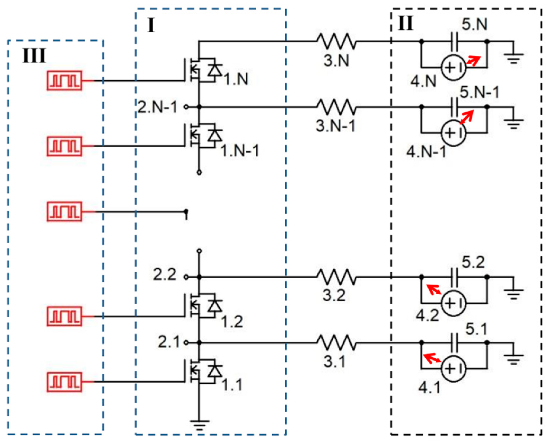
The flowchart of HV pulse generators includes three main units depicted as I, II, and III in Figure 1. Unit I consists of N transistors (1.1–1.N) connected by N-1 electrical contact (2.1–2.N-1) sequences. Unit II consists of N-regulated HV sources of power (4.1–4.N) shunted by N capacitors (5.1–5.N). Unit III controls the gates of transistors in N×MOSFET (N×IGBT or devices with cascode configuration [14]). N resistive loads (i.e., 3.1–3.N) of the N transistors (1.1–1.N) connect Units I and II.
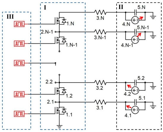
Figure 1.
The patented design of HV pulse generators [25].
A thorough analysis of the current state-of-the-art basic circuits and their variations (for example, [1,2,3,4,5,20,21,22,23,24]) reveals the innovative and surprisingly simple design of HV generators proposed in [25,26]. The new architecture does not solve the issue of synchronous operation on transistor gates in Unit I, nor does it resolve the challenges of a specific implementation of Unit II.
Looking ahead, we note that experimental new generators with low-cost HV SiC MOSFETs provide switching with voltage slew rates of more than 100 kV/µs for quasi-rectangular pulses at an effective repetition rate of about 7 MHz. SPICE modeling shows that it is possible to achieve voltage slew rates of about 500 kV/µs for modern HV transistors.
3. Voltage/Current Distributions in Circuits of New Generators
In new generators, the mechanisms that ensure normal operation of HV transistors in the serial stack manifest themselves differently in steady-state and transient modes. Modeling of the circuit behavior allows one to find out the characteristics of switching in specific circuit architectures. The solutions of Kirchhoff equations for the electrical equivalent circuits (Figure 2 and Figure 3) indicate the process parameters for OFF and ON steady-states.
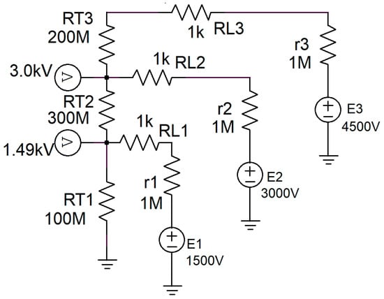
Figure 2.
Voltages in the equivalent circuit of new generators with 3×MOSFET stack in OFF state.
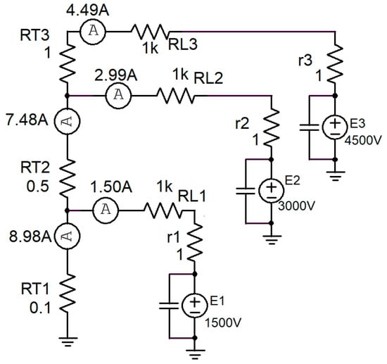
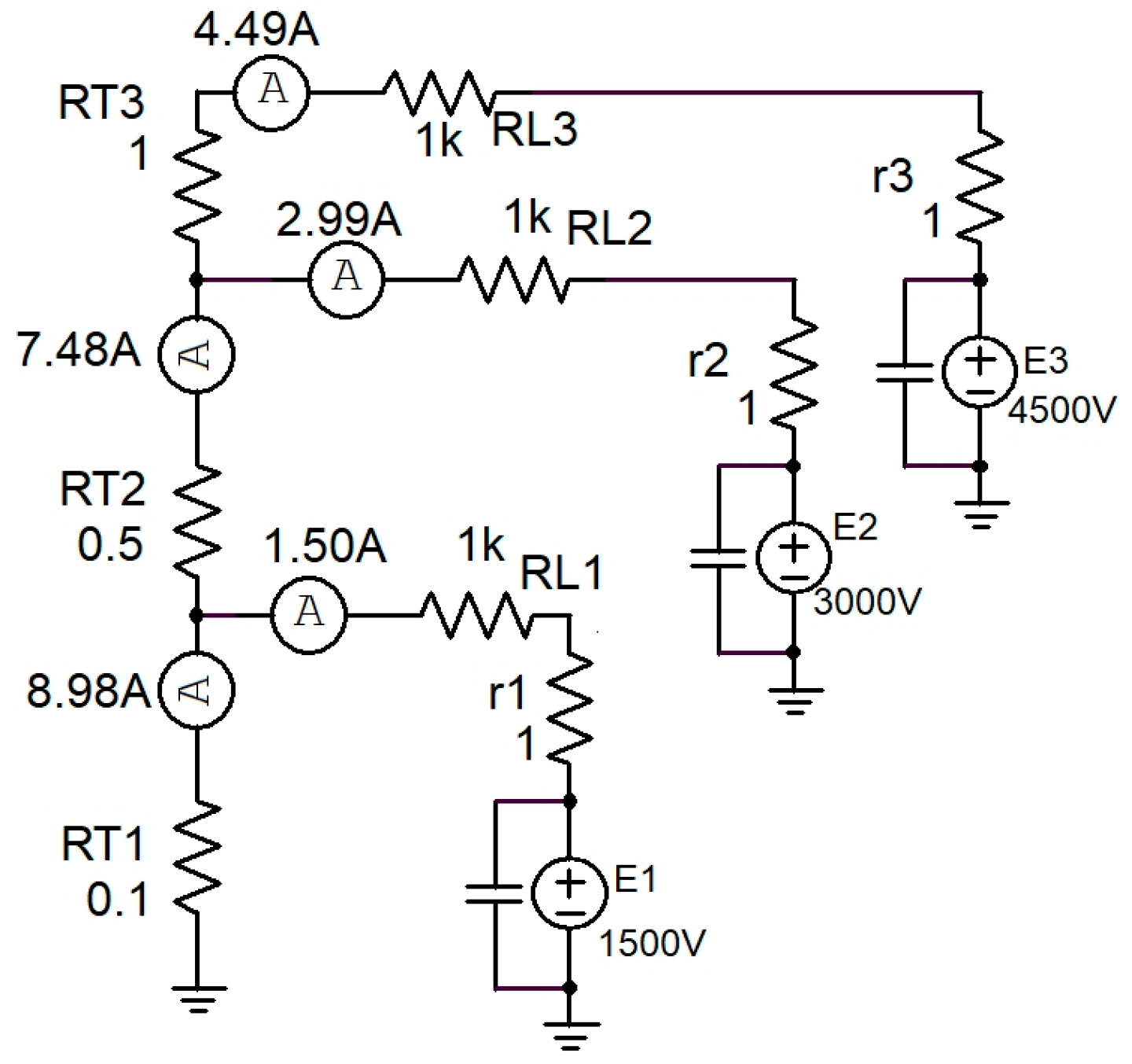
Figure 3.
The distribution of currents in the equivalent circuit of new generators with 3×MOSFET stack in ON steady-state.
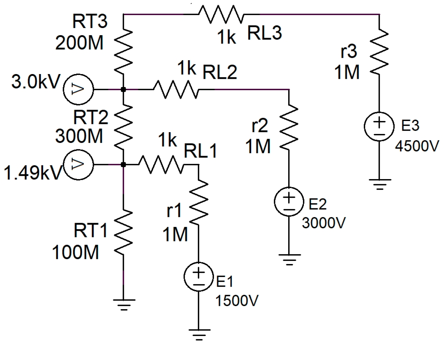
3.1. Equivalent Circuit with 3×MOSFET in OFF Steady-State
For the OFF state of new generators, the main interest is the voltage distribution on transistors. Figure 2 shows the equivalent circuit of a generator in OFF state. The sources of regulated HV power (E1, E2, and E3) have effective internal resistances, depicted as r1, r2, and r3. These resistors may be about 1 MΩ. In these conditions, the E sources with voltages of about 5 kV can produce a constant current of ~5 mA. Datasheets typically provide zero gate voltage drain currents (IDSS) for Umax, allowing for the estimation of transistor resistances (RT1, RT2, and RT3) in OFF state. For example, STP4N150 transistors (Umax = 1.5 kV) have IDSS = 10−5 A [9], and OFF-resistors are ~108 Ω.
Multisim software (of 14.3 version) simulations show a high quality of voltage equalization/balancing when the stack is in OFF state: all transistors (T1, T2, and T3) with a large variation of resistance values (RT) appear to be under the same voltage.
3.2. Equivalent Circuit for New Generators in ON Steady-State
In ON state, it is necessary to maintain appropriate currents on transistors in order not to overload them. The position of Ti transistor in N×MOSFET relative to the ground node (G) determines the current (ITi) of Ti transistor. The closer the Ti transistor is to G-node, the more that current flows through it.
In HV SiC transistors, typical ON state resistances range from 0.1 to 10 Ohm. This is much lower than the transistor loads. HV sources have low effective impedances because large capacitors are connected to them in parallel. The latter provide significant pulse currents through the open channel of transistors. Figure 3 shows the results of the electrical circuit simulation for ON steady-state (dc current) of 3×MOSFET.
The simulation results show that the currents (ITi) flowing through the transistors in 3×MOSFETs are:
i.e., IT1 current is determined by summation, even if all transistors of the stack have different resistances in ON state.
IT3 = E3/RL3, IT2 = IT3 + E2/RL2, IT1 = E3/RL3 + E2/RL2 + E1/RL1
3.3. Disadvantage of Proposed Concept
Let us assume that for all HV sources (Figure 3), the value of Ei is an integer multiple of E1 = E, where E represents the voltage difference on all transistors in a stack. If all load resistances, RL1, RL2, RL3, etc., satisfy the condition that they are equal RL, then the current IT1 through the T1 node (1) will be:
IT1 = (3E + 2E + E)/RL
For a stack with identical N transistors and identical loads, Equation (2) takes the form of
IT1 = (E/RL) (N + … + 2 + 1) = (E/RL) (N + 1)∗(N/2)
On the contrary, for a conventional stack (with a single load RL) under the corresponding voltage N∗E, the current IT1 is N∗E/RL, i.e., it is (N + 1)/2 times smaller than in Equation (3). Multipliers of order (N + 1)/2 are a disadvantage of the new technical solution. Therefore, the application area of the proposed concept is most likely not industrial electronics. The field of high-speed instrumental applications with their relatively low operational currents and significant demands on the quality of functional performance is promising.
3.4. Equivalent Circuit in Steady-State at Desynchronization of Transistor Switching
One of the beneficial aspects of the concept is the decreased voltage overload of the T1 transistor, which delays ON→OFF transition compared to other transistors in the stack. This is because each transistor has its own HV power source and load resistance.
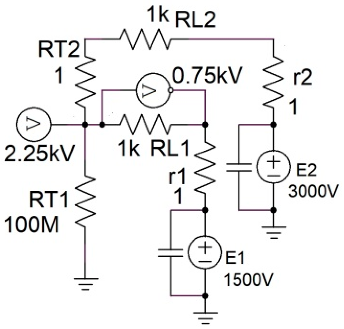
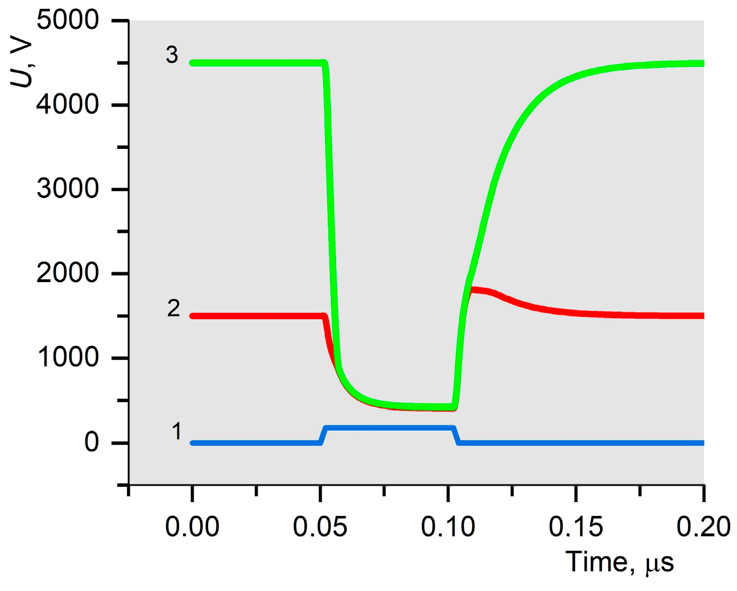
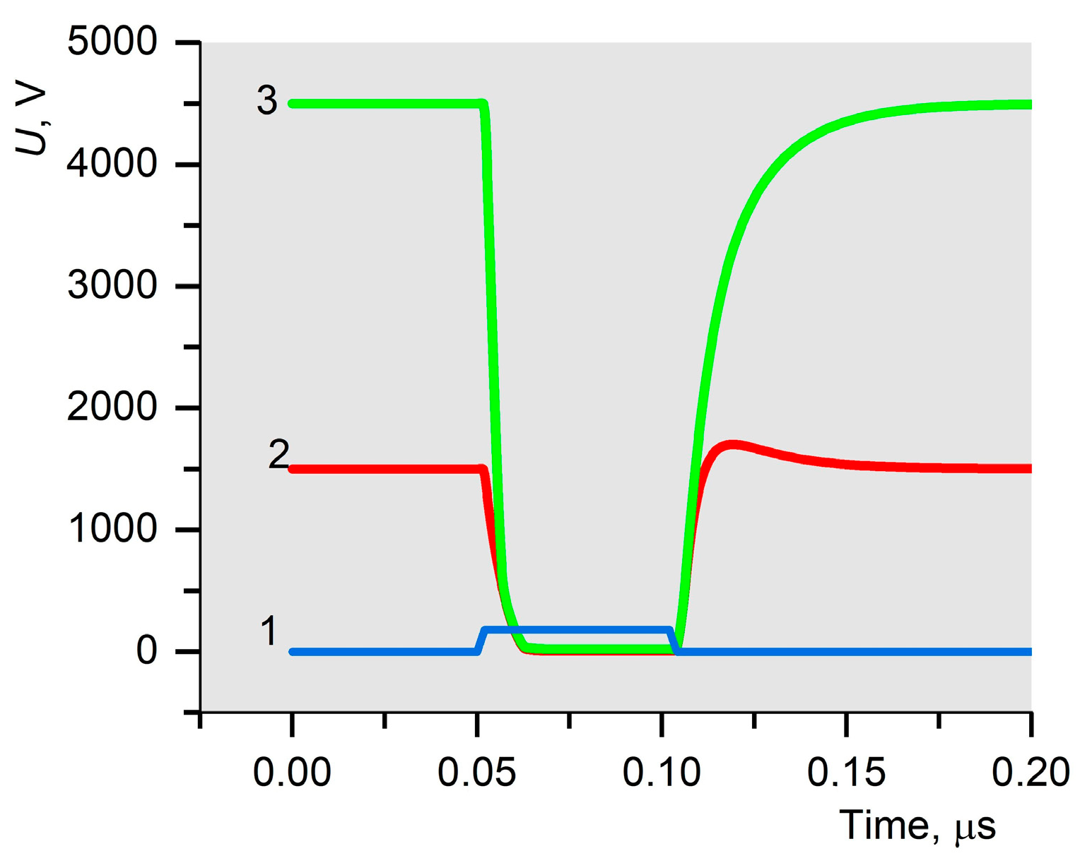
Let us consider the case of 2×MOSFET stack in which the T2 transistor is in ON stationary state while T1 with Umax = 1.5 kV is still in OFF state. The voltage overload on transistor T1 is shown in Figure 4. This overload is 2.25 kV − 1.5 kV = 0.75 kV but not 3 kV − 1.5 kV = 1.5 kV, as it would be in a conventional generator.
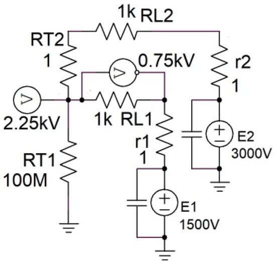
Figure 4.
The reduction of overvoltage on the T1 transistor (from 1500 V to 748 V) is due to the corresponding voltage drop on RL1 load.
The reduction in the overload results in a voltage drop across RL1 load of the T1 transistor. Therefore, in this specific case, the overload for the T1 transistor, which lags the transition from OFF to ON, is half the voltage it would be in a standard circuit with a single total load.
3.5. Equivalent Circuit at Desynchronization in Transient Switching Mode
Below, we demonstrate the high quality of voltage balancing across stack transistors during transient switching modes. The presented data relate to test experiments and circuit modeling using SPICE models of modern HV transistors. As the load resistance increases, ON→OFF transition time also increases. To verify the proposed concept in dynamic modes, we need transistors capable of fast switching between states. Information on the required transistors can be found in datasheets and by using computer SPICE models at transient circuit simulation.
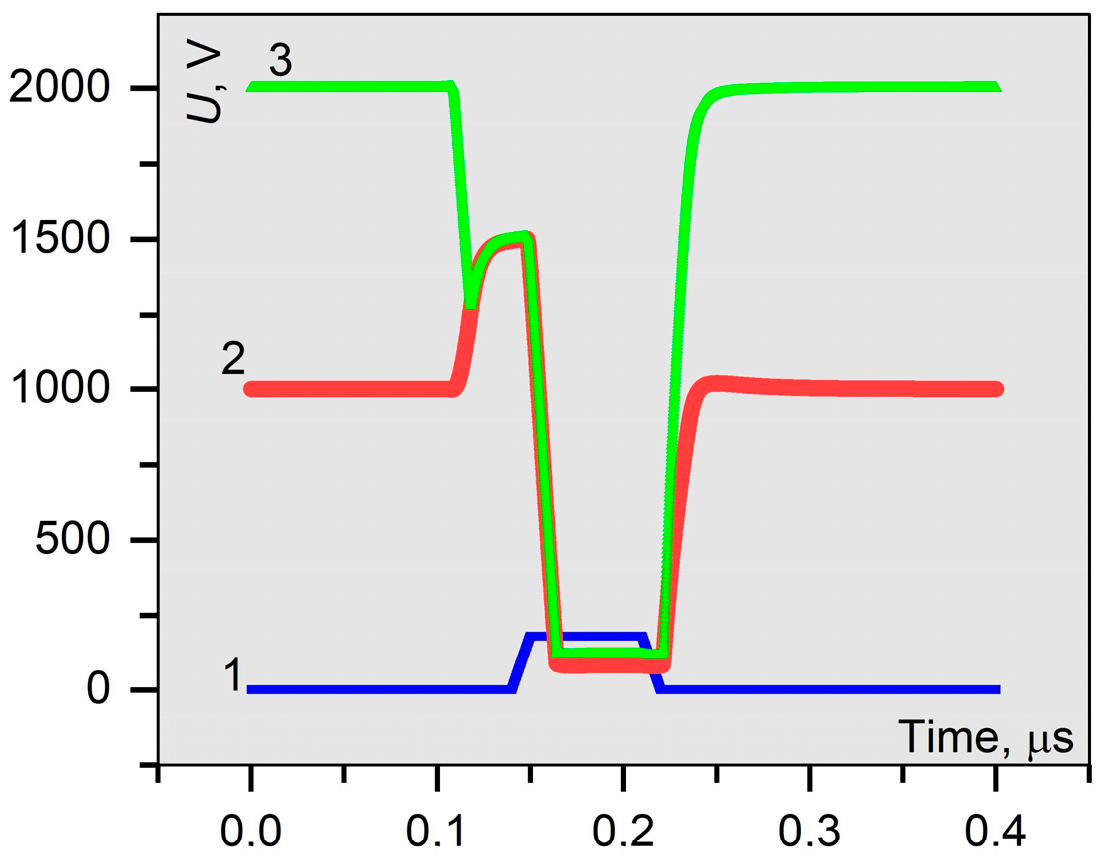
The time delay for the t transistor relative to the T2 in OFF→ON transient mode (circuit as in Figure 4) is shown in Figure 5 for E1 = 1000 V and E2 = 2000 V. The Micro-Cap program simulates the operation of 2×STP4N150 circuit with RL1 and RL2 being 400 Ω loads. In new generators, transistor T1 is under less voltage overload than what can occur in conventional generators.
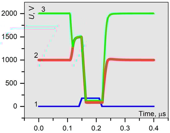
Figure 5.
Overload reduction from 1000 V to 500 V for the T1 transistor in 2×STP4N150 stack, which operates in dynamic mode (the scheme for modeling is as in Figure 4). 1 (blue): gate voltage waveform T1 (10× magnification); 2 (red): drain voltage waveform T1; 3 (green): drain voltage waveform T2.
4. Modeling/Experimental Testing for Verification of Proposed Concept
To convincingly validate the proposed concept of voltage balancing, HV transistors with fast switching must be involved in modeling/experimental testing. This implies a pre-selection among different types of MOSFETs that are faster than IGBT devices.
For HV rectangular pulse generators, the design of PCB is such a complex task that it is necessary to take into account small stray capacitances and inductances to a greater extent than in the case of low-voltage (LV) electronics. If PCB is not properly designed, undesirable effects can occur in the circuit [27], which will distort HV pulses. For example, if the pulse amplitude is 10 kV and the pulse rise time is about 10 ns, then the parasitic capacitance of 10 pF on TN transistor drain creates a current of about 5 A through the stack. Such a value is comparable to the working pulse current. In these conditions, parasitic capacitance can distort the shape of a quasi-rectangular pulse due to the overcurrent of the T1 transistor. To the best of the authors’ knowledge, among the many PCB design software, only Altium [28] (version 25) checks PCB layouts against HV design rules.
Under these conditions, it is difficult to properly and comprehensively verify the new circuit concept in experimental tests for different types of fast transistors. Therefore, this study focuses on modeling different variants of schemes. The circuit simulation programs (such as Multisim: v. 14.3, Micro Cap: v. 12.2, LTspice: v. 24, QSpice: v. 08/16/2024, and PSIM: v. 2024.0.0247) provided tests of switching for HV SiC transistors. We also present experimental test data. For instance, experimental generators with wire connections between circuit elements in their design achieved high switching speeds with a high repetition rate.
4.1. Pre-Selection of Fast Transistors
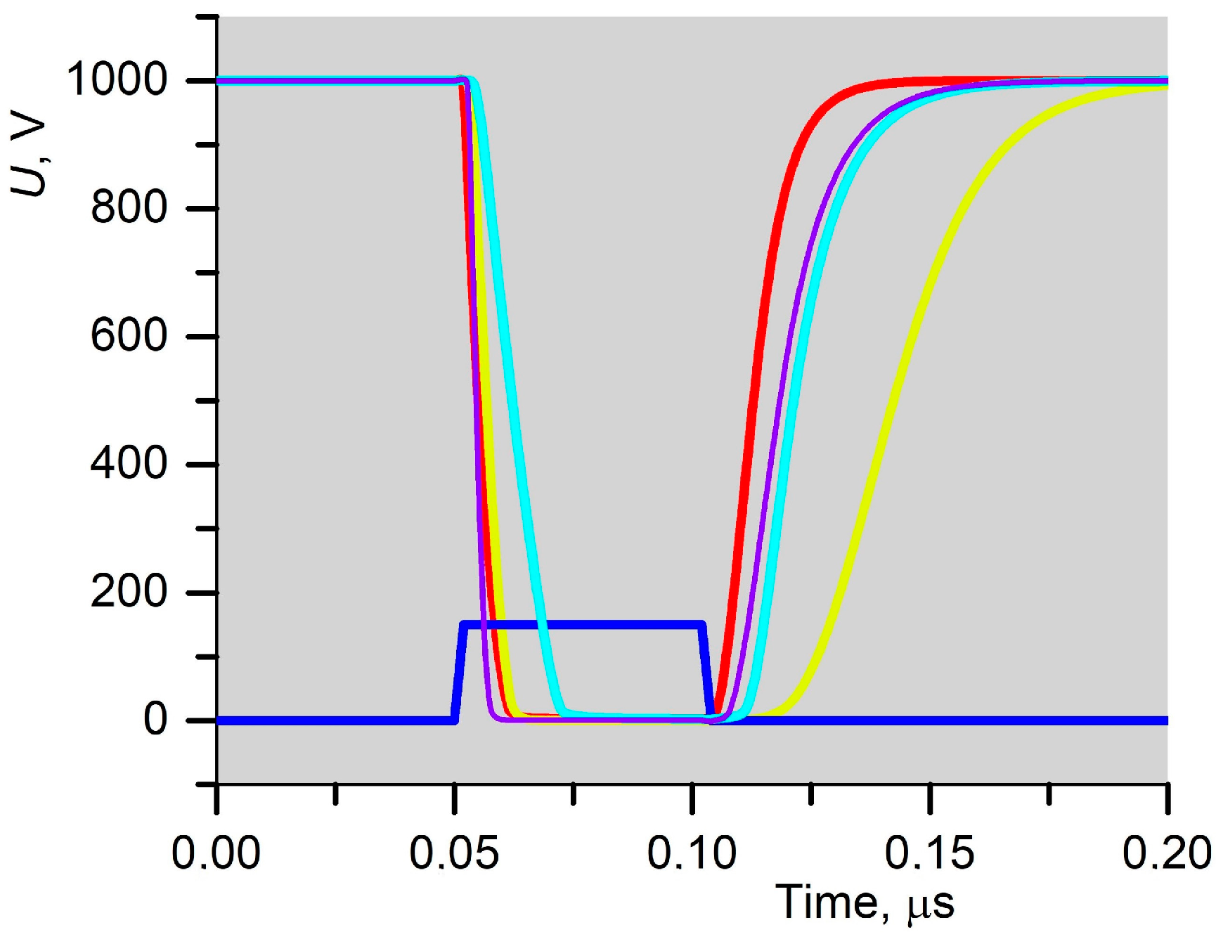
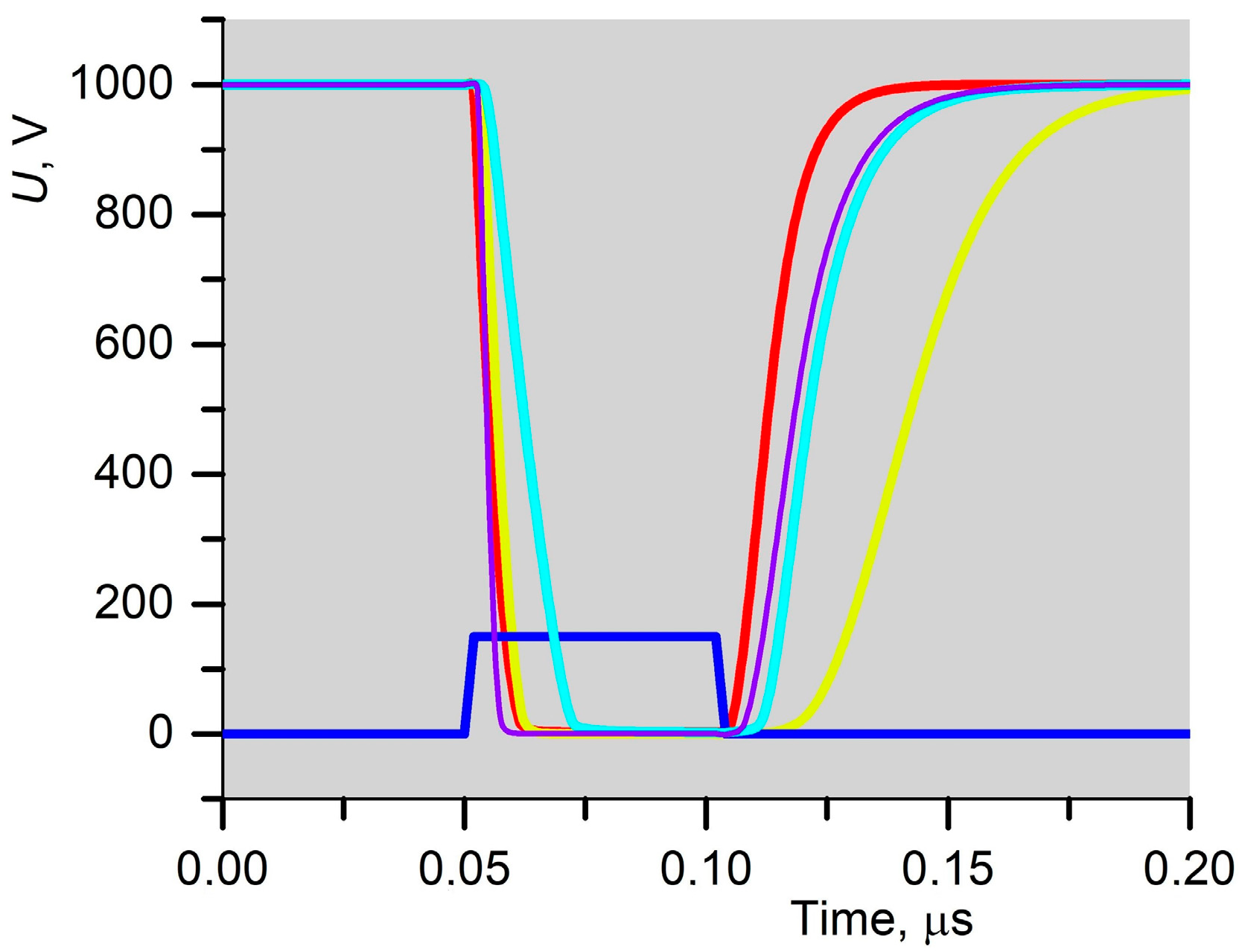
Figure 6 and Figure 7 show the results of the comparative modeling (LTspice). Only waveforms of SiC transistors STP4N150 (STMicroelectronics, [9]), SCT1000N170 (STMicroelectronics) and G2R1000MT33J (GeneSiC Semiconductor [12]) are indicated, as they were selected for experimental verification of the proposed voltage-balancing concept.

Figure 6.
The simulated switching waveforms of some modern SiC transistors (different manufacturers). The voltage waveforms for gates (blue, 10× magnification) as in Figure 5. Red: the voltage on the drain of SCT1000N170 transistor, selected for further tastings. Other transistors are not mentioned for ethical reasons (they were not selected for further comparative testing).

Figure 7.
The comparison of simulated switching waveforms of some modern SiC transistors (different manufacturers). Pulses on the gates of transistors (blue, 10×), as in Figure 5 and Figure 6. Red: the voltage on SCT1000N170 drain; yellow: the voltage on STP4N150 drain. Other transistors are not mentioned for ethical reasons.
The GeneSiC [12] offers encrypted models of transistors that are only suitable for LTspice/PLECS programs, while the new and growing Qspice program [14] currently contains cascode models and only a few other HV transistors in its library. The selected transistors have the following characteristics: STP4N150, which is the low-cost and high-switching-speed transistor: Umax = 1.5 kV, pulsed drain current 12 A; SCT1000N170: Umax = 1.7 kV, pulsed drain current 20 A; and G2R1000MT33J: Umax = 3.3 kV, pulsed drain current 10 A.
Figure 6 and Figure 7 demonstrate that the switching of the selected HV transistors do not differ significantly in terms of rise and fall times, as well as turn-on (and turn-off) delay times. According to the simulation (Figure 8), the slew rate of STP4N150 at turn-on is approximately equal to the same value for the SCT1000N170 transistor; the G2R1000MT33J is a better choice, while the HV IXTT1N450HV ([13]) transistor (Umax = 4.5 kV) shows a noticeably lower switching speed (it can be suitable for an operation at the microsecond scale).

4.2. Pre-Selection of Transistors for Experimental Stacks: New Methodology
If the proposed voltage balancing concept was tested by simulating the operation of a stack with identical transistors, the verification methodology would be considered questionable. Indeed, for identical transistors, all SPICE models are identical, and if real transistors had identical parameters, voltage balancing would not make sense at all.
Our original methodology for verifying the new concept of HV balancing in series-connected fast transistors involves modeling the behavior of stacks with transistors that are not of the same but different types. Balancing the stacks during the transitions between OFF and ON is difficult using conventional techniques based on resistors, snubber circuits, varistors, and other similar components. This is true for techniques that use gate-side controls, which need to take into account different transistor types and operating modes. In this context, the new concept has no limitations; it seems quite simple, universal, and reliable.
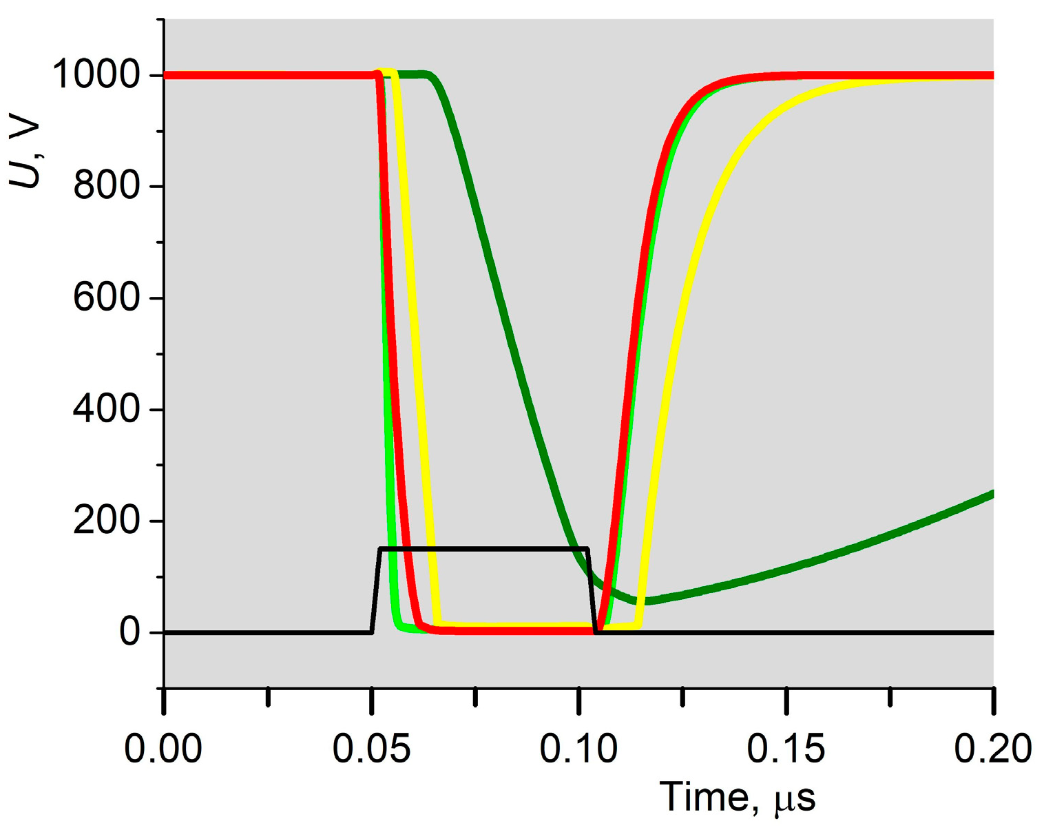
Figure 9 and Figure 10 show the simulation results in LTspice (v. 24) for two new generators with different stacks. Figure 9 corresponds to the case when one SCT10000N170 transistor is on the T1 site and G2R1000MT33J is on the T2 site. In Figure 10, two SCT10000N170 transistors (connected in parallel) are on the T1 site, while G2R1000MT33J is on the T2 site (the circuit is shown in Figure 11).

Figure 9.
The simulation-switching voltage waveforms for the new generator with 2×MOSFET stack. 1: pulses on the gates of transistors (blue, 10×); 2: SCT1000N170 transistor at the T1 site (red); 3: G2R1000MT33J transistor at the T2 site (green).
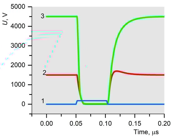
Figure 10.
The simulation stitching for the new generator with a hybrid stack. 1 (blue): voltage pulses on gates of transistors (10×); 2 (red): the voltage waveform on drains of two parallel-connected SCT1000N170 transistors at the T1 site; 3 (green): the voltage waveform on the drain of the G2R1000MT33J transistor at the T2 site.
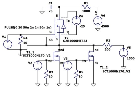
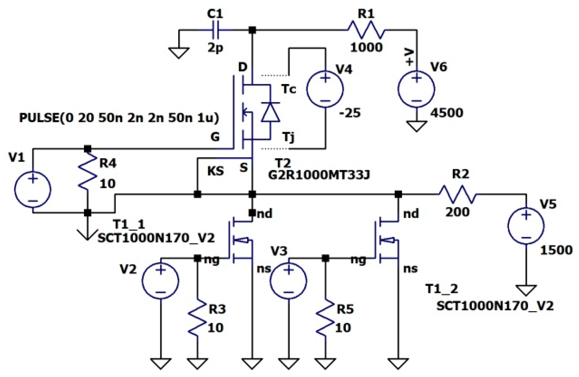
Figure 11.
The circuit of the new generator with the hybrid dual-cascade stack (two SCT10000N170 transistors at the T1 site and one G2R1000MT33J transistor at the T2 site).
A comparison of Figure 9 and Figure 10 captures a disadvantage of new generators: the closer the transistor is to the ground node (G), the more current flows through it. To overcome this feature, we need, for example, to put two transistors at the T1 site. This will reduce the average current amplitude through each transistor, increase the pulse amplitude, and improve the shape of quasi-rectangular HV pulses. Note that if the number or type of transistors changes at the T site, new schematics enable flexible customization of the stack by adjusting resistive loads.
Component C1 (Figure 11) symbolizes the unavoidable parasitic capacitance; it strongly affects the current flowing in high-speed switching stacks. Hence, the issue of PCB design for rectangular HV pulse generators is topical.
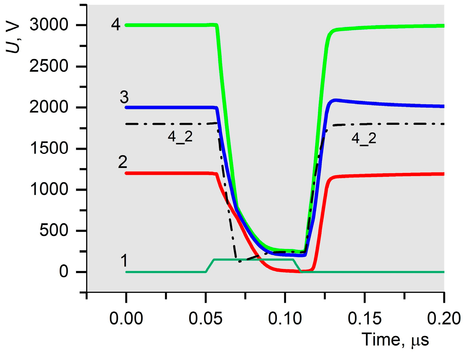
To show how effective the proposed concept is, we have simulated the drain voltages for a stack consisting of three very different series-connected HV transistors. The results are shown in Figure 12.

Figure 12.
Voltage balancing on series-connected transistors of different types in the new generator. 1 (thin dark green): Pulses on gates of all transistors (10×); 2 (red): the voltage waveform for the drain of UF3C170400K3S cascode transistor at the T1 site; 3 (blue): the voltage waveform for the drain of STP4N150 at the T2 site; 4 (bold light green): the voltage waveform for the drain of STP4N150 at the T3 site (green). The 4_2 sign (black, dash-dotted) denotes the difference between T3 and T1 voltage waveforms (Qspice simulations).
The UF3C170400K3S transistor is a composite device in which a normally-on SiC JFET is combined with Si-MOSFET to produce a normally-off SiC-FET hybrid. In the modeled stack operation, STP4N150 transistors are on T2 and T3 sites. Note: due to the different currents on the T2 and T3 sites, the corresponding same-type transistors have different resistance at the identical voltage difference, i.e., they are in different states.
4.3. Balance Processes in Conventional Generators vs. in Proposed Concept
Let us examine in more detail the scenarios of processes involved in voltage equalization/balancing within a stack, in which transistors (T1, T2, …, TN) may exhibit differences in characteristics. Two possible cases are considered: (●) a single common load RL serves the entire stack; (●●) “individual” loads RLi serve each transistor Ti of the stack (according to the proposed concept).
- The case of OFF→ON transitions.
(●) During the transition (most of the time t), any Ti transistor in the stack has a resistance RTi(t) significantly larger than RL. Therefore, in the specified time interval, the voltage from Ti is redistributed not to RL load but to transistors in the stack that are at earlier stages of OFF→ON transition. This process can cause the stack to break down.
(●●) If each stack transistor has its own individual RLi load, then for a long period of time during the transient process, each resistance RTi(t) satisfies the ratio: RTi(t)~RTk(t) >> RLi. In this case, transient currents flow through all loads, and the voltages are redistributed between the corresponding pairs (Ti and RLi). Such localized processes do not significantly affect each other, even if transistors block different voltages in the OFF state.
- The case of ON→OFF transitions.
(●) In a stack with a single RL load, for any Ti and Tk transistors, RTi(t)~RTk(t) >> RL during a long part of the transition time. Therefore, the voltage redistribution occurs during the process of freeing the devices from excess charge carriers, when charges pass through the entire sequence of transistors.
(●●) If each Ti transistor in the stack has an individual load RLi << RTk(t), then the Ti transistor will be released from excess charge via RLi. This process is faster than transferring charge through a sequence of megaohm transistors, as in the case of a single common load (RL).
Thus, if all stack transistors have their own “individual” loads, then the processes of voltage redistribution in dynamic modes follow less resistive paths. The disadvantage of the proposed new solution is increased currents on transistors with small “i” indices, e.g., T1. Transistor parallelism partially solves the problem. Another disadvantage is an enhanced power consumption of multi load stacks.
5. Experimental Generators: Developing and Testing
5.1. Generator Based on 2×STP4N150 with Umax = 1500 V
According to preliminary computer simulation results, the STP4N150 and G2R1000MT33J transistors took part in test experiments to obtain data confirming the operational advantages of the proposed voltage-balancing concept. The quality of voltage balancing across stack transistors decreases significantly with increasing voltage slew rate. Therefore, it is important that new generators can operate reliably under transistor-switching challenging conditions.
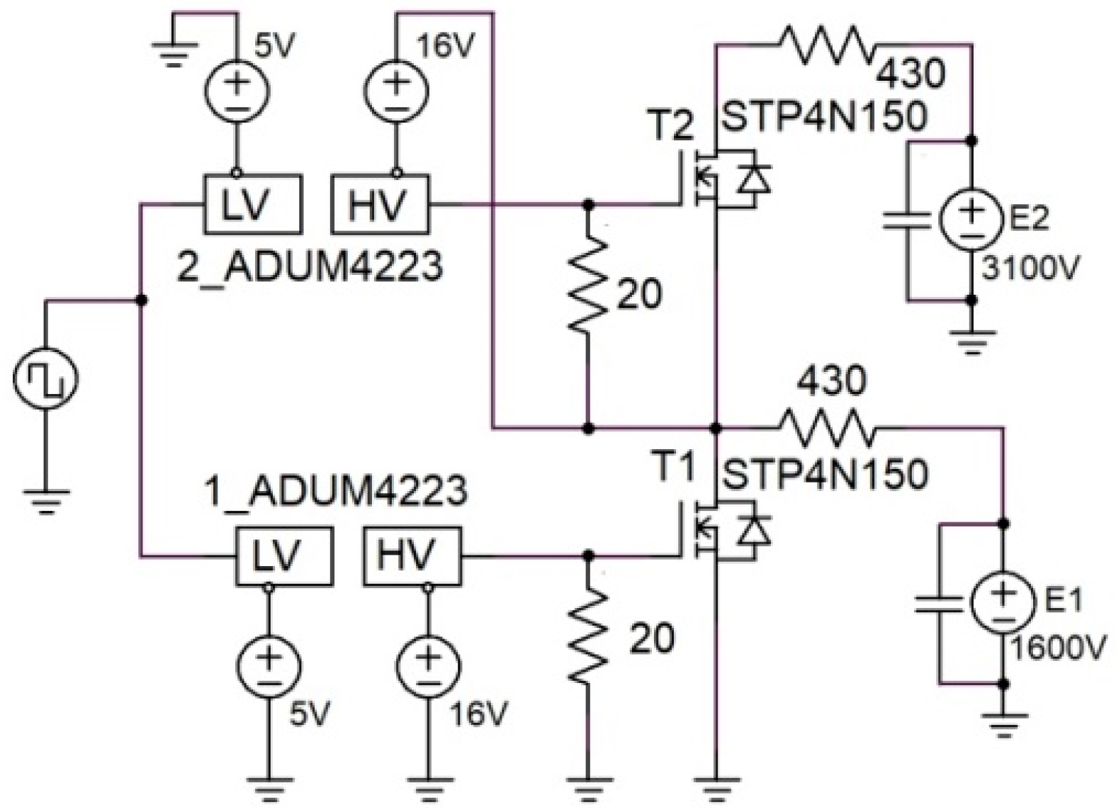
Figure 13 shows the generator with 2×STP4N150 and two HV drives of ADUM4223 type (Unit III). HV isolation separates the input low voltage (LV) and output HV sections of the drivers. The monolithic transformers transmit signals between the LV and HV sections in ADUM4223 chips. Autonomous miniature 16 V sources power the HV section of drivers. We pre-selected drivers based on the results of signal propagation delay measurements. This allowed the drivers to synchronously drive the gates of STP4N150 SiC MOSFETs.
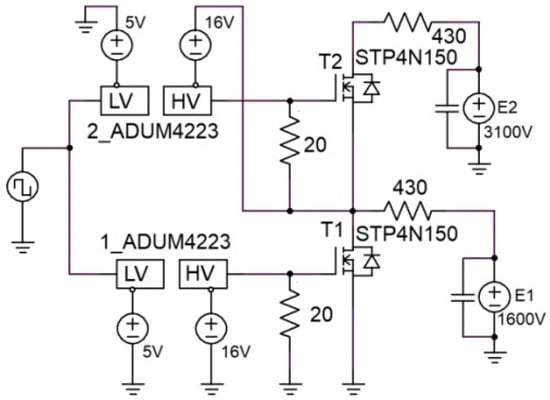
Figure 13.
The new generator with two STP4N150 transistors (rated at 12A drain pulsed current and Umax = 1500 V).
With two selected ADUM4223 drivers or two selected HV UCC21520 drivers, new generators produce single, high-quality rectangular HV pulses. Moreover, owing to high-quality HV equalization, ADUM4223 chips have demonstrated the ability to drive the gates of STP4N150 transistors at an effective frequency of more than 7 MHz. This is seven times the maximum data rate with a minimum pulse width of 50 ns specified in the datasheet for ADUM4223 chip.
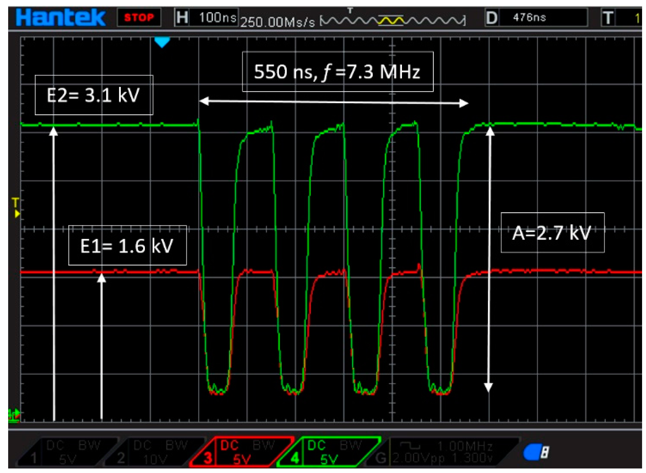
Figure 14 shows voltage waveforms for the generator with 2×STP4N150, where pulses are initiated by two ADUM4223 drivers. In the OFF state of both STP4N150 transistors, it was possible to set supply voltages that are slightly (50–100 V) higher than their Umax. In other words, during the switching processes, the voltage on the 2×STP4N150 was slightly higher than the maximum allowable voltage for the stack (extremely challenging transient test). Modeling in Micro-Cap 12 confirmed the experimental data obtained. The model of the new generator in the OFF state used E1 = 1600 V and E2 = 3100 V on the T1 and T2 transistors, respectively.
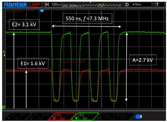
Figure 14.
Voltage waveforms on drains of two STP4N150 transistors in the new generator (experiment). Scales are 500 V/div and 100 ns/div. HV probes are 1:100. Red: the waveform for the drain of STP4N150 at the T1 site. Green: the waveform for the drain of STP4N150 at the T2 site.
We also confirmed the switching stability of the circuit (Figure 13) under the following conditions: two STP4N150 transistors (connected in parallel, rated at 24A total pulsed drain current) or one STW9N150 transistor (rated at 32A pulsed drain current) operated at the T1 site. It is important to note that after replacing the MOSFETs, no circuit reconfiguration was required. The observed situation is very different from that expected for other voltage equalization techniques using resistive dividers, snubbers, varistors, etc.
5.2. Two Generators Based on G2R1000MT33J Transistors with Umax = 3300 V
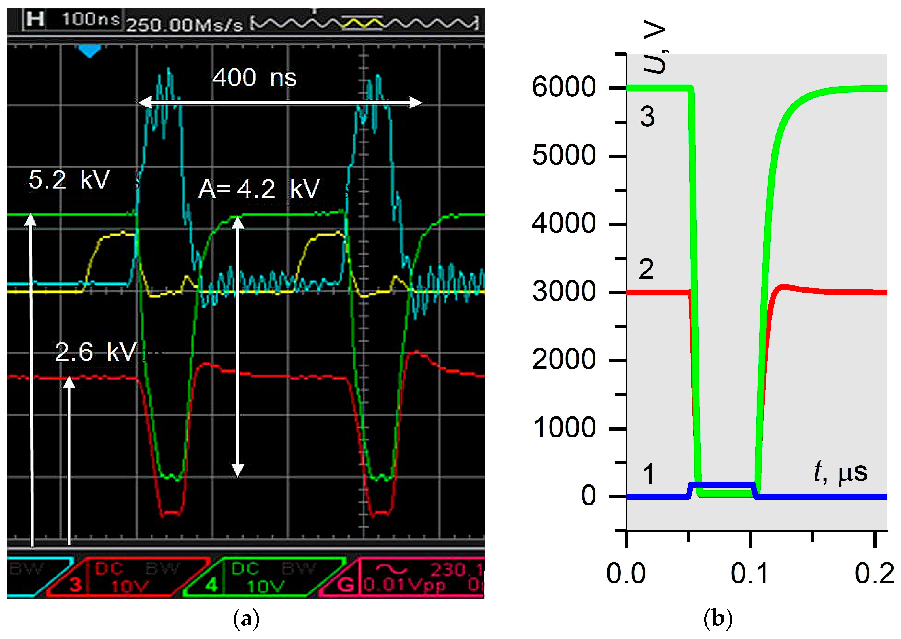
Figure 15a,b illustrates the operation (experimental test and corresponding LTspice simulations) for two generators, in which stacks contain the G2R1000MT33J transistors (rated for a pulsed drain current of 10 A) at the T1 and T2 sites. In the case of Figure 15a, the circuit was as it is depicted in Figure 13, with two G2R1000MT33J transistors. The resistive loads were R1 = 860 Ω and R2 = 860 Ω, while E1 = 2.6 kV and E2 = 5.2 kV. The quality of the rectangular pulses depends on the current at the T1 site. The simulation shows, in Figure 15b, that if two transistors are connected in parallel at the T1 site, the amplitude and quality of the rectangular pulses significantly increase.
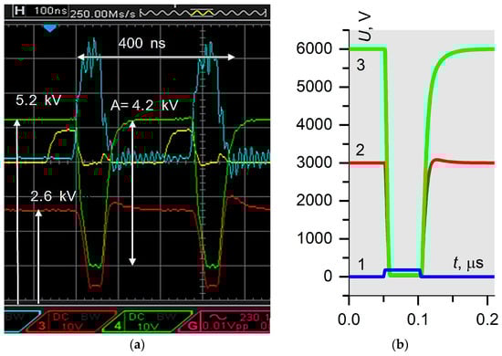
Figure 15.
Verification of operational efficiency of new generators. (a) Experimental voltage waveforms on the drains of G2R1000MT33J transistors in two cascade stacks of new generators (the circuit as in Figure 13 with R1 and R2 loads of 860 Ω). Scales are 1 kV/div and 100 ns/div. HV probes are 1:100. Red waveform: the voltage on the transistor drain at the T1 site. Green waveform: the voltage on the transistor drain at the T2 site. Yellow waveform: the input signal for both ADUM4223 drivers. Cyan waveform: the voltage on the output of 1_ADUM4223 driver. (b) Simulated voltage waveforms on the drains of G2R1000MT33J transistors in two cascade stacks with two paralleled transistors at the T1 site (the circuit as in Figure 11 with loads R1 = 200 Ω and R2 = 1 k Ω). Scales are 1000 V/div and 100 ns/div. 1: pulses on gates of two paralleled transistors at the T1 site (blue, 10× magnification); 2: the waveform for the combined drain of two G2R1000MT33J transistors at the T1 site (red); 3: the waveform for the drain of G2R1000MT33J at the T2 site (green).
By using STP4N150 and G2R1000MT33J transistors, the series-connected stacks were able to generate quasi-rectangular pulses with peak voltages of 2.7 kV and 4.2 kV. In these cases, slew rates greater than 100 kV/μs were attained at turn-on and turn-off processes (for comparison, see [29]). For 2×STP4N150 stack, the effective frequency was higher than 7 MHz. The results of HV waveform modeling showed that the switching speed for hybrid series-parallel stacks with two cascades can reach a slew rate of 500 kV/µs. The proposed innovations demonstrate reliable performance in challenging conditions. An example is fast switching near the safe operating area (SOA) and N × Umax limit voltages applied to the stack.
Thus, as proven by modeling and experimental testing, the novel concept resulted in excellent HV balancing across the stacks in new HV rectangular pulse generators.
6. Conclusions
The design of stacks, easily and flexibly adapted to any type of high-speed transistors, is an urgent task. The technical result from the proposed concept of reliable voltage balancing on a stack of fast high-voltage (HV) transistors creates the following advantages:
- The voltage on each transistor can be very close to the nominal maximum Umax. This ensures reliable operation, enhances the amplitude of HV pulses, minimizes the rise/fall time transients, and attains a high pulse frequency.
- The new circuits are simple and can be easily customized/modified to meet different requirements. The circuits can contain transistors with different Umax ratings. Transistors in parallel increase the power of pulses without changing any other parts of the circuit.
- The creation of new HV pulse generators does not demand knowledge of the subtleties of the functioning of snubbers, experience in the adjustment of series-connected stacks, or skills relating to sophisticated gate-side control techniques.
The main disadvantage of new HV generators is the summation of currents flowing through all transistor loads. The closer the T transistor of the stack is to a ground (G) node, the more current flows through it. Therefore, the application area of the proposed concept is most likely not industrial electronics but rather the field of high-speed instrumentation with its relatively low operating currents and significant quality requirements for functional performance.
In this work, we only briefly examined the consequences of current flowing through a grounded (G) transistor of a stack. This current is (N + 1)/2 times larger than in a traditional technical solution. Also, issues related to connecting additional HV sources, increasing electromagnetic interference, thermal management, and circuit design complexity in terms of controlling various parasitic components have not been investigated. The ability of the new generator to provide HV pulses coupled with high currents requires further research. This includes the important question of the frequency and power limit for the proposed new HV generator architecture.
GaN discrete FETs offer outstanding speed and power, and the advances will continue to expand the frequency range and increase power level. However, there are two points to consider. First, technological progress in extremely high frequency operation is achieved by reducing the gate length in GaN devices; this path is limited for HV FETs but not for power and HV electronics based on serial-connected transistors. Second, SiC still operates at higher voltages than GaN. Therefore, in this study, we have not systematically applied the concept of HV balancing to GaN FETs. Trial simulations (LTspice, v. 24) for hybrid series-parallel stacks using three GaN GPIHV30SB5L [10] transistors, as in Figure 11, demonstrate a high level of voltage balancing. Switching slew rates of this hybrid stack were higher compared to a similar stack with three SiC G2R1000MT33J transistors. A total blocking voltage of 2 kV was on both types of stacks.
Overcoming and eliminating the drawbacks associated with trade-offs is the inevitable fate of any technical solution, which is never universal but fulfills with guarantee its main target functions. The proposed innovations perform their core functions excellently and will facilitate new research on yet unexplored topics. The new conception of HV balancing and generator architecture are simple, versatile, and efficient in their main functions. For this reason, the innovation has the features of basic circuits of power and HV electronics, high-speed instrumentation (for examples, see [2,16,17]), and nanosecond biomedical treatments [30,31]. In fact, the proposed circuit can “extract” the ultimate speed characteristics from any transistor in a stack.
The significance of the proposed and verified HV balancing concept is useful to consider from different general points of view. Expert committees often have to address the relative scientific merit of findings. The article [32] proposes a quantitative framework for such deliberations, and it argues that the degree of surprise of an experimental result is an adequate metric for evaluating the scientific merit. This thesis is consistent with [33], that while the number of publications grows exponentially, the “cognitive extent of science” (the number of different unique concepts) increases only linearly.
Author Contributions
Conceptualization, A.D. (Alexandr Despotuli); methodology, A.D. (Alexandr Despotuli), V.K., A.D. (Anastasia Despotuli) and A.A.; experimental investigation, A.D. (Alexandr Despotuli) and A.D. (Anastasia Despotuli); software and computer modeling, A.D. (Alexandr Despotuli), A.D. (Anastasia Despotuli) and A.A.; resources, A.D. (Alexandr Despotuli), V.K. and A.A.; writing—original draft preparation, A.D. (Alexandr Despotuli) and A.D. (Anastasia Despotuli); writing—review and editing, A.D. (Alexandr Despotuli), V.K., A.D. (Anastasia Despotuli) and A.A. All authors have read and agreed to the published version of the manuscript.
Funding
This research was funded by STATE TASK No. 075-00295-25-00.
Data Availability Statement
The original contributions presented in the study are included in the article, further inquiries can be directed to the corresponding author.
Conflicts of Interest
The authors declare no conflicts of interest.
Abbreviations
The following abbreviations are used in this manuscript:
| HV | high-voltage |
| FET | field-effect transistor |
| SiC | silicon carbide |
| MOSFET | metal-oxide-semiconductor field-effect transistor |
| PCB | printed circuit board |
| IGBT | insulated-gate bipolar transistor |
| SOA | safe operating area |
References
- Zhuge, Y.; Liang, J.; Fu, M.; Long, T.; Wang, H. Comprehensive overview of power electronics intensive solutions for high-voltage pulse generators. IEEE Open J. Power Electron. 2023, 5, 1–20. [Google Scholar] [CrossRef]
- Abadi, M.R.Q.R.; Marzebali, M.R.; Abolghasemi, V.; Anisi, M.H. High-voltage pulse generators for electroporation application: A systematic review. IEEE Access 2022, 10, 64933–64951. [Google Scholar] [CrossRef]
- Withanage, R.; Shammas, N. Series connection of insulated gate bipolar transistors (IGBTs). IEEE Trans. Power Electron. 2012, 27, 2204–2212. [Google Scholar] [CrossRef]
- Frivaldsky, M.; Zelnik, R.; Spanik, P. Design proposals for high-voltage stacked configuration GaN module. Electronics 2024, 13, 3198. [Google Scholar] [CrossRef]
- Zhao, W.; Ghafoor, S.; Lagerweij, G.W.; Rietveld, G.; Vaessen, P.; Niasar, M.G. Comprehensive investigation of promising techniques to enhance the voltage sharing among SiC MOSFET strings, supported by experimental and simulation validations. Electronics 2024, 13, 1481. [Google Scholar] [CrossRef]
- Langpoklakpam, C.; Liu, A.-C.; Chu, K.-H.; Hsu, L.-H.; Lee, W.-C.; Chen, S.-C.; Sun, C.-W.; Shih, M.-H.; Lee, K.-Y.; Kuo, H.-C. Review of silicon carbide processing for power MOSFET. Crystals 2022, 12, 245. [Google Scholar] [CrossRef]
- Chen, Z.; Huang, A.Q. Extreme high efficiency enabled by silicon carbide (SiC) power devices. Mat. Sci. Semicon Proc. 2024, 172, 108052. [Google Scholar] [CrossRef]
- Available online: https://www.wolfspeed.com/products/power/sic-mosfets/1700v-silicon-carbide-mosfets/c2m1000170d/ (accessed on 11 February 2025).
- Available online: https://www.st.com/en/power-transistors/stp4n150.html (accessed on 11 February 2025).
- Available online: https://iganpower.com/ganhemts (accessed on 11 February 2025).
- Available online: https://www.infineon.com/cms/en/product/power/mosfet/silicon-carbide/discretes/imyh200r100m1h/ (accessed on 11 February 2025).
- Available online: https://navitassemi.com/genesic-mosfets-products/ (accessed on 11 February 2025).
- Available online: https://www.littelfuse.com/products/power-semiconductors-control-ics/mosfets-si-sic/n-channel-standard/very-high-voltage (accessed on 11 February 2025).
- Available online: https://www.qorvo.com/design-hub/design-tools/interactive/qspice (accessed on 11 February 2025).
- Bolotnikov, A.; Losee, P.; Permuy, A.; Dunne, G.; Kennerly, S.; Rowden, B.; Stevanovic, L. Overview of 1.2kV–2.2kV SiC MOSFETs targeted for industrial power conversion applications. In Proceedings of the 2015 IEEE Applied Power Electronics Conference and Exposition (APEC), Charlotte, NC, USA, 15–19 March 2015; pp. 2445–2452. [Google Scholar] [CrossRef]
- Bemius, M.T.; Chutjian, A. High-voltage, full-floating 10-MHz square-wave generator with phase control. Rev. Sci. Instrum. 1989, 60, 779–782. [Google Scholar] [CrossRef]
- Baker, R.J.; Johnson, B.P. Stacking power MOSFETs for use in high-speed instrumentation. Rev. Sci. Instrum. 1992, 63, 5799–5801. [Google Scholar] [CrossRef]
- Available online: https://www.behlke.com/pdf/general.pdf (accessed on 21 February 2025).
- Available online: https://www.paramerus.com/pages/hvpg.php (accessed on 21 February 2025).
- Abbate, C.; Busatto, G.; Iannuzzo, F. High-voltage, high-performance switch using series-connected IGBTs. IEEE Trans. Power Electron. 2010, 25, 2450–2459. [Google Scholar] [CrossRef]
- Rutten, T.P.; Wild, N.; Veitch, P.J. Fast rise time, long pulse width, kilohertz repetition rate Q-switch driver. Rev. Sci. Instrum. 2007, 78, 073108. [Google Scholar] [CrossRef] [PubMed]
- Son, M.; Lee, T.; Kwon, S.; Cho, Y. Impact of snubber parameters on voltage sharing in series-connected insulated gate bipolar transistors. J. Pow. Elect. 2020, 20, 1002–1014. [Google Scholar] [CrossRef]
- Alves, F.S.; Lefranc, P.; Jeannin, P.-O.; Sarrazin, B. Advanced voltage balancing techniques for series-connected SiC-MOSFET devices: A comprehensive survey. Power Elect. Dev. Compon. 2024, 7, 100055. [Google Scholar] [CrossRef]
- Wang, R.; Jørgensen, A.B.; Liu, W.; Zhao, H.; Yan, Z.; Munk-Nielsen, S. Voltage balancing of series-connected SiC mosfets with adaptive-impedance self-powered gate drivers. IEEE Trans. Indust. Electron. 2023, 70, 11401–11411. [Google Scholar] [CrossRef]
- Despotuli, A.L.; Kazmiruk, V.V.; Despotuli, A.A.; Andreeva, A.V. Generator of High-Voltage Rectangular Pulses. Patent RU № 2 819 031. Available online: https://patenton.ru/patent/RU2819031C1 (accessed on 11 February 2025).
- Despotuli, A.L.; Kazmiruk, V.V.; Despotuli, A.A.; Andreeva, A.V. A generator of rectangular pulses based on a serial connection of mosfet with Umax = 4500 V. Instrum. Exp. Technol. 2024, 67, 54–61. [Google Scholar] [CrossRef]
- Persson, E.; Di Domenico, F. Optimizing PCB layout for HV CoolGaN power transistors. AN_2306_PL52_2308_151809. Available online: https://www.infineon.com/dgdl/Infineon-CoolGaN_High_voltage_power_transistors_for_PCB_layout_optimization-ApplicationNotes-v01_00-EN.pdf?fileId=8ac78c8c8929aa4d0189ba64ffb262a2&da=t (accessed on 11 February 2025).
- Available online: https://files.resources.altium.com/sites/default/files/2022-09/file_665%5B1%5D.pdf (accessed on 11 February 2025).
- Okuda, T.; Nishimura, Y.; Nishioka, K.; Kishimoto, S.; Kikuchi, Y.; Nakamura, T. A 5-kV pulse generator with a 100-kV/µs slew rate based on series-connected 1700-V SiC MOSFETs for electrical insulation tests. Rev. Sci. Instrum. 2021, 92, 114705. [Google Scholar] [CrossRef] [PubMed]
- Achour, Y.; Starzynski, J.; Jakubiuk, K. New architecture of solid-state high-voltage pulse generators. Energies 2022, 15, 4823. [Google Scholar] [CrossRef]
- Novickij, V.; Rembiałkowska, N.; Szlasa, W.; Kulbacka, J. Does the shape of the electric pulse matter in electroporation? Front. Oncol. 2022, 12, 958128. [Google Scholar] [CrossRef] [PubMed]
- Knuteson, B. A quantitative measure of experimental scientific merit. Available online: https://arxiv.org/abs/0712.3572 (accessed on 11 February 2025).
- Fortunato, S.; Bergstrom, C.T.; Börner, K.; Evans, J.A.; Helbing, D.; Milojević, S.; Petersen, A.M.; Radicchi, F.; Sinatra, R.; Uzzi, B.; et al. Science of science. Science 2018, 359, aao0185. [Google Scholar] [CrossRef] [PubMed]
Disclaimer/Publisher’s Note: The statements, opinions and data contained in all publications are solely those of the individual author(s) and contributor(s) and not of MDPI and/or the editor(s). MDPI and/or the editor(s) disclaim responsibility for any injury to people or property resulting from any ideas, methods, instructions or products referred to in the content. |
© 2025 by the authors. Licensee MDPI, Basel, Switzerland. This article is an open access article distributed under the terms and conditions of the Creative Commons Attribution (CC BY) license (https://creativecommons.org/licenses/by/4.0/).