1. Introduction
Energy crises and environmental concerns give rise to the need to save energy. A lot of researchers have looked into renewable sources to find solutions; others focus on building new power architecture to meet the competing requirements in the aspects of performance, efficiency, and cost. Among most of the renewable energy sources, wind power accounts for a large portion. However, electric voltage from wind generators are usually AC based whereas general appliances are DC based such as computers, light emitted diode (LED), audio and video equipment. In the past, they are converted into DC by a rectifier which implies additional loss. Also, the voltage generated from the generator is high voltage, whereas the voltages needed for home and office are DC and are lower voltage. A step down converter is needed that also requires additional subcircuits. Besides the high power wind generator, the low power wind generator based on a distributed power concept is now popular for office and home uses, such that small wind turbines are attached to windows for wind energy capture.
A conventional switched-mode power converter [
1] consisting of both a inductor and capacitor has not demonstrated significant improvement in last 10 years, whereas the switched capacitor based power converter using single energy storage has been found to be suitable for power conversions and conditionings, because it does not require bulk magnetic energy storage devices [
2,
3,
4,
5,
6] and can eliminate the high frequency inductor [
7]. Its novelty lies in that it only requires a capacitor and switches. The main advantage of this kind of converter is that capacitors as the energy storage element are small. Hence, it is possible to fabricate a small size and lighter weight miniature package or even integrated circuit [
8,
9]. In [
10,
11], the switched capacitor based converter is applied to a battery management system to decrease the system size and to solve the problem of the flat voltage curve of some types of lithium-ion batteries. In [
12], a switched capacitor based AC-DC converter suitable for small-scale wind power generation systems is proposed to obtain both rectification and high voltage gain.
However, one of the drawbacks of the switched capacitor converter is high current spikes when the capacitor is charging and discharging. If the conversion ratio changes significantly, more capacitors and switches are required. That means that more current spikes will be generated and more gate driving circuits are employed. It will cause more electromagnetic interference (EMI) and loss. It also complicates the circuit. Series and parallel resonant networks were used in the circuit to reduce the power loss, and EMI, meanwhile increasing power efficiency [
13,
14,
15]. Higher charging and discharging current spikes could be decreased by introducing small resonant inductors [
6], which significantly reduce the power loss and increase efficiency. However, more switches employed still cause more loss of state.
Another shortcoming of this kind of converter is voltage regulation. The output voltage depends on the number of switched capacitor cells since the switched capacitors are charged to a certain voltage firstly then are released to the load. Therefore, regulation is difficult. One way to overcome this is to use the equivalent series resistance of the capacitor and the resistance of the transistor when it is on as a resistor-capacitor (RC) charging and discharging control [
3]. The drawback of such a method is an increase in switching losses since the transistor does not operate in a saturation region. These converters are therefore usually used only for lower power and are operating at lower efficiency (80% or less). The efficiency also deteriorates seriously as the switching frequency increases.
In this paper, a family of novel resonant converters is presented. It is based on switched capacitor step up/down cells which maintain the characteristic of high power efficiency to overcome the drawbacks of the conventional Buck-boost converter with low efficiency under higher step down. Meanwhile, it provides another conversion ratio, 2
n/m, which makes the voltage conversion range wider and more flexible. It lessens the disadvantage of the switched capacitor based power converter. It consists of only two switches and a number of switched capacitor cells depending on the output voltage required. Both switches are operating under the zero current switching condition by the resonance of the capacitors and an introduced small inductor. It significantly reduces the switching loss and EMI. Each switched capacitor cell consists only of switched capacitors and diodes. The capacitor is used to store energy; the diode is used to assist in the direction of the power flow. By increasing the number of switched capacitor cells, the different step up or step down voltage conversion ratios which vary more than the conventional switched capacitor converters can be obtained [
16,
17,
18,
19]. The current spike can be eliminated, hence the EMI is reduced, and the efficiency is improved.
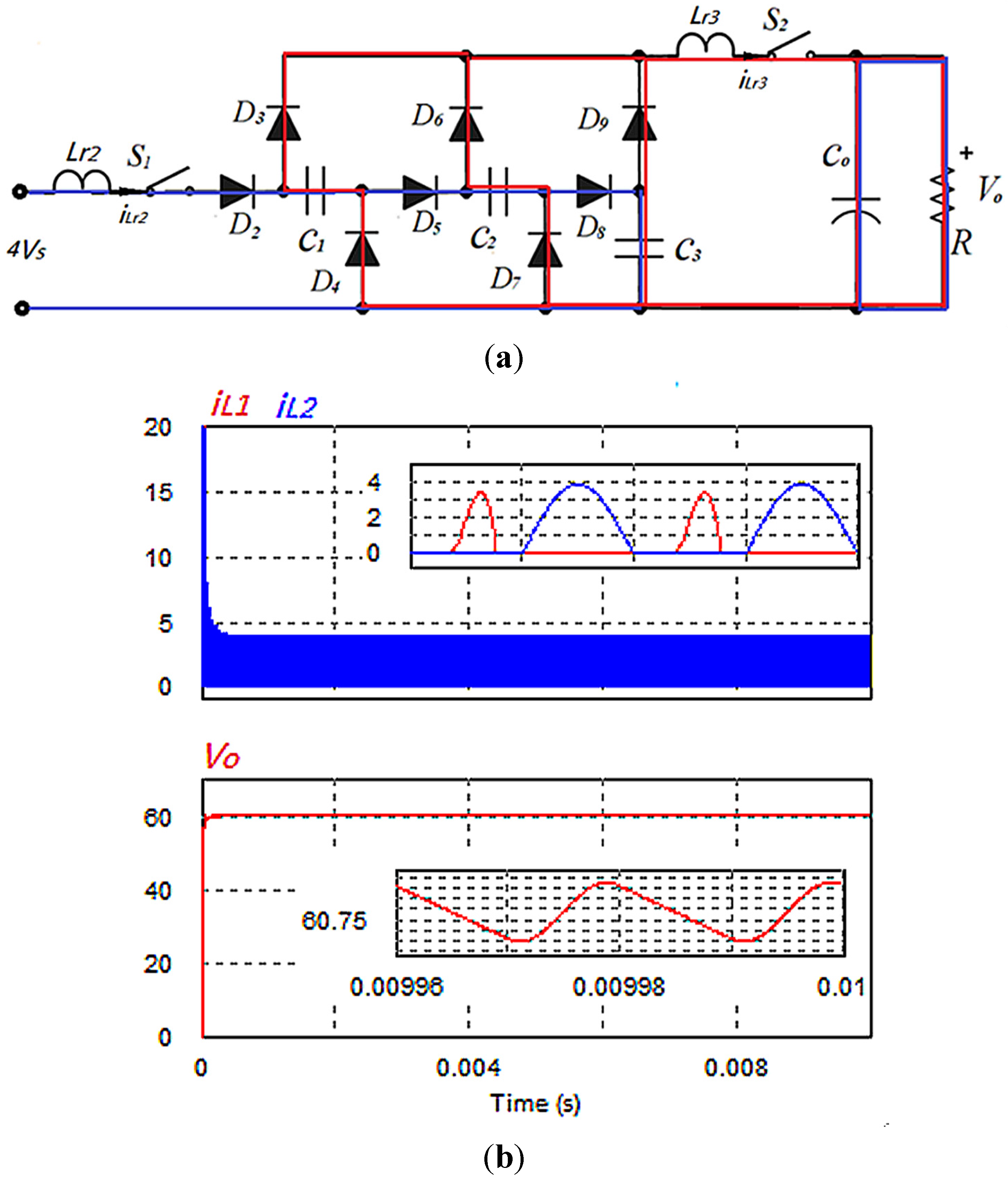
Figure 1 shows the basic step up and down circuit and the step up/down cells, respectively. The general proposed resonant step up/down circuit is shown in
Figure 2. After a detailed analysis and comparison of operation principles, the generalized analysis and equations of the switched capacitor resonant step up/down power converter is presented. The proposed circuit is suitable for low to high power wind generation, and is good for a distributed low power generator as well because the bulky inductor can be eliminated. The starting point of this investigation of the proposed technology is to rectify the AC voltage from generator to DC. A high frequency AC is examined because current wind generators tend to be higher frequency in order to reduce the machine size.
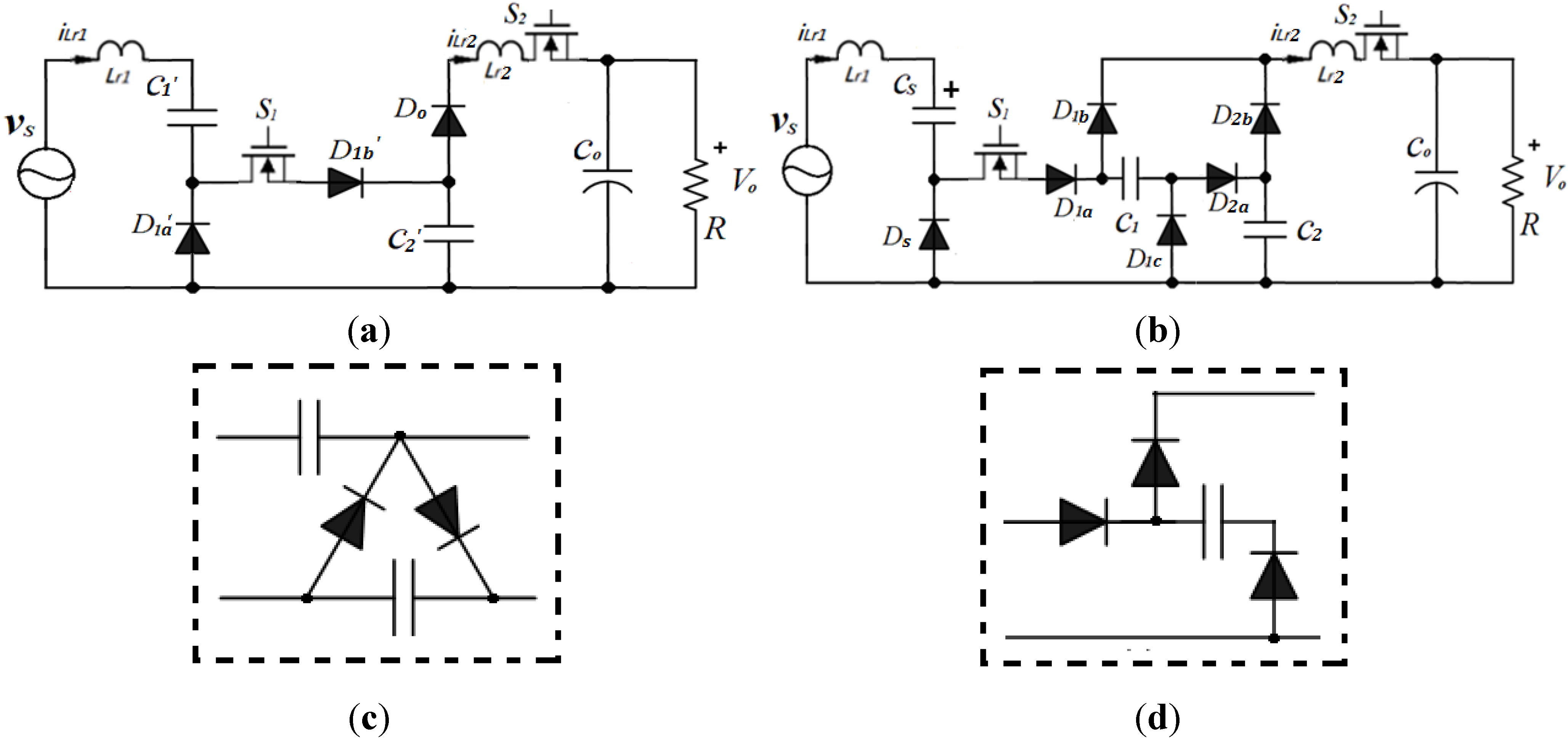
Figure 1.
The basic step up and down circuit and switched capacitor cell for step up and step down: (
a) basic step up version; (
b) basic step down version; (
c) step up cell [
20]; and (
d) step down cell [
7].
Figure 1.
The basic step up and down circuit and switched capacitor cell for step up and step down: (
a) basic step up version; (
b) basic step down version; (
c) step up cell [
20]; and (
d) step down cell [
7].
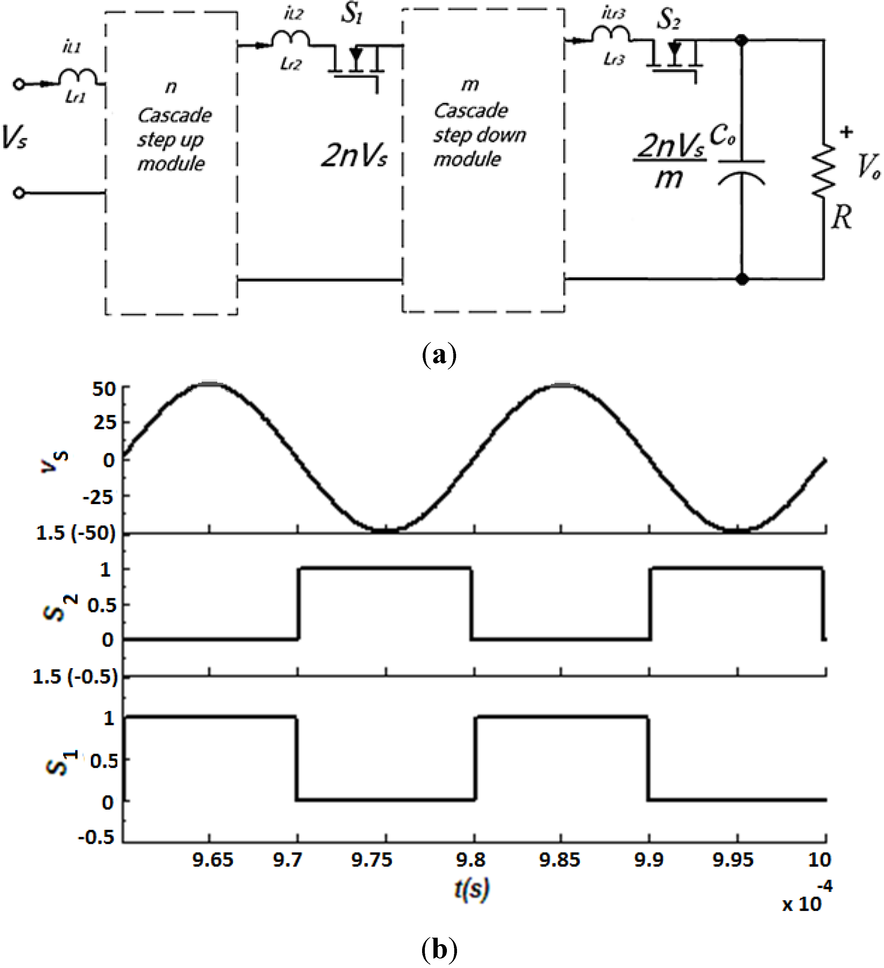
Figure 2.
The source voltage, driving signal and cascade module: (a) the general circuit of the proposed step up/down circuit; and (b) the source voltage and the driving signal.
Figure 2.
The source voltage, driving signal and cascade module: (a) the general circuit of the proposed step up/down circuit; and (b) the source voltage and the driving signal.
2. Principle of the Proposed Step Up/Down Resonant Converters
The basic topologies of the proposed resonant circuit are shown in
Figure 1. It shows the step up resonant power converter as shown in
Figure 1a and step down resonant converter as shown in
Figure 1b. The switched capacitor C
1′ is charged up in the step up resonant power converter. Then, it acts as the power source of the step down switched capacitor power converter to release the energy to the load. The capacitors in the step down converter are charged up in series then release the energy to the load in parallel. Hence, the output voltage is shared by the switching capacitor cells. The voltage is stepped up by introducing cascaded step up switching capacitor cells, as shown in
Figure 1c, and stepped down by step down switching capacitor cells, as shown in
Figure 1d. The
2n stepping up switched capacitor cells and m stepping down cells are connected in a series by using two Metal–Oxide–Semiconductor Field-Effect Transistors (MOSFETs), as shown in
Figure 2a. By alternatively turning on and off the two switches, the overall voltage conversion ratio 2
n/m can be obtained. Hence, the voltage conversion ratio is wider than the conversion ratio
n, 1/
n. The principle of driving signal is shown in
Figure 2b.
By introducing three small inductors, resonant tanks can be formed and zero current switching (ZCS) can be achieved [
5]. It will eliminate current spikes when capacitors are charging and discharged.
3. Operation Principles of the Proposed Circuit
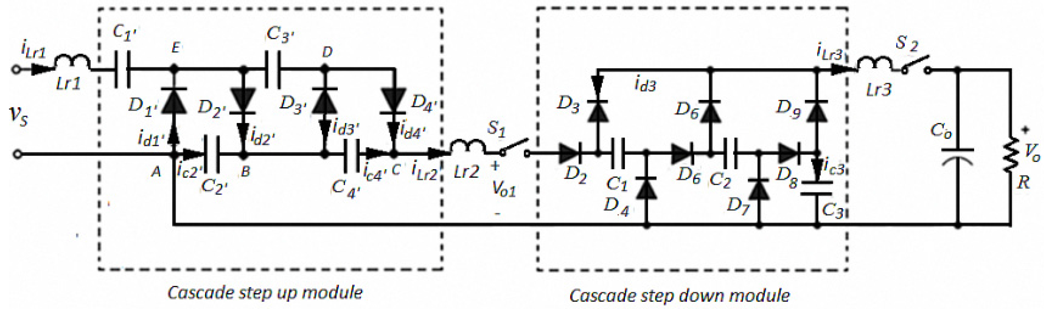
A two step up cell and three step down cell resonant switching capacitor power conversion circuit is presented in
Figure 3. The circuit can be analyzed by stepping up the module and stepping down the module individualy. Small resonant inductors are introduced to reduce the current stress of the components.
Figure 3.
A two step up cell, three step down cell switched capacitor AC-DC converter.
Figure 3.
A two step up cell, three step down cell switched capacitor AC-DC converter.
3.1. n Step Up Cells
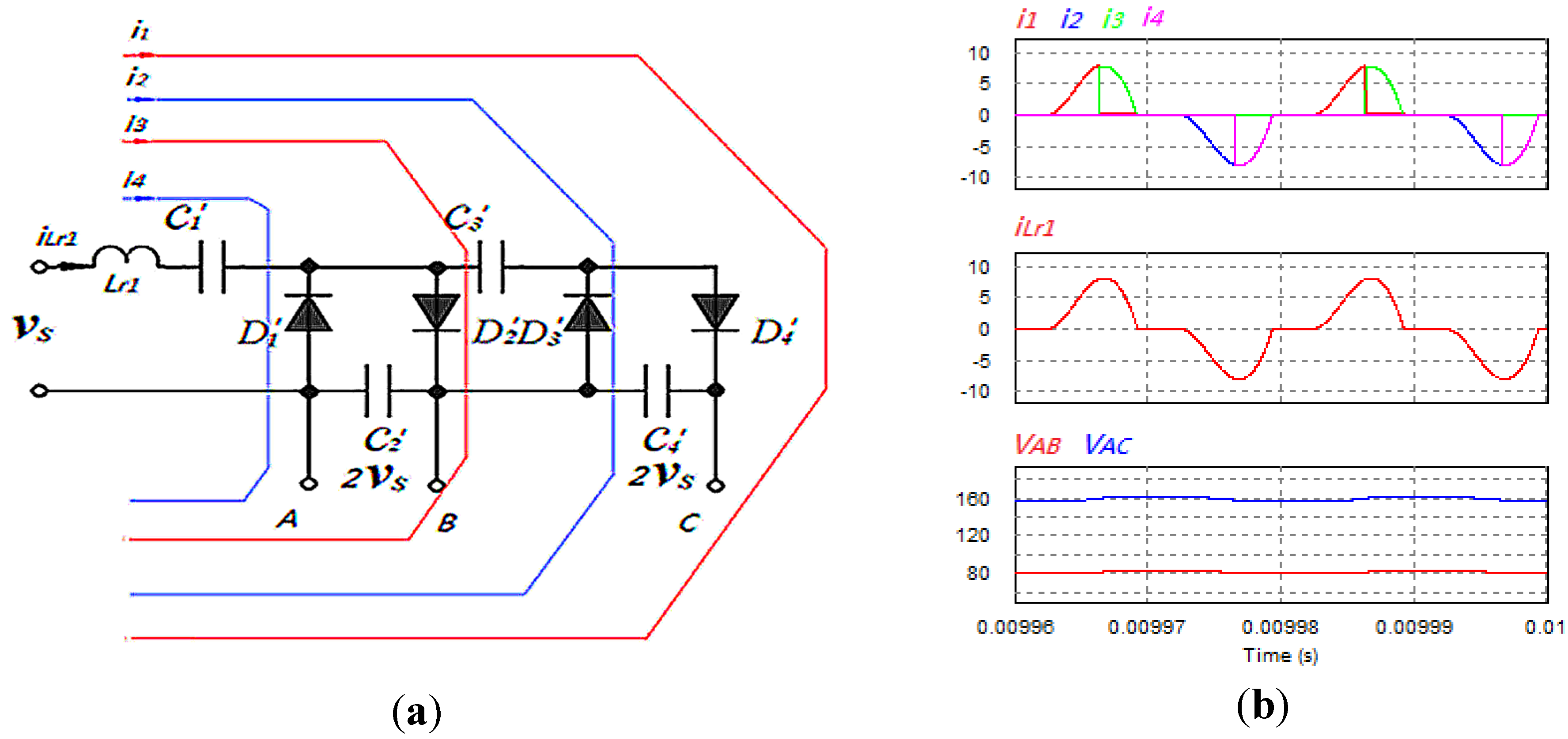
As it is shown in
Figure 3, the cascaded step up module is similar to a half-wave series voltage multiplier, as shown in
Figure 4a. It is simple and no driving signal is needed. By plugging in a number of switched capacitor cells, the 50 V, 50 kHz high frequency AC input voltage can be stepped up to different voltages. As shown in
Figure 4a, by flexibly choosing connection point AB or AC, different output voltages can be achieved. By introducing a very small inductor, the capacitors C
1′ and C
3′ are slowly charged through diodes D
1′ and D
3′ and in turn, the current increases slowly from zero and resonate back to zero as shown in
Figure 4b by the resonant tank. The input voltage is stepped up through the stepping effect of coupling capacitors C
1′, C
3′, C
2′ and C
4′. The stepped up voltage is an even multiple of input voltage. The voltages between A, B and A, C are 2
Vs and 4
Vs respectively, are shown in
Figure 4b;
i.e., the conversion ratio is 2
n.
Figure 4.
(a) A two stage AC voltage multiplier; and (b) the current and voltage of a two step up cell module.
Figure 4.
(a) A two stage AC voltage multiplier; and (b) the current and voltage of a two step up cell module.
3.2. m Step Down Cells
The cascaded step down module is a resonant switched capacitor step down converter, as shown in
Figure 5a. By alternatively turning on and off the two switches, the switched capacitors C
1, C
2 and C
3 are charged in series and from a resonant tank with inductor L
r2. the charging currents
iLr1 resonates in sinusoidal waveform. Then, the capacitors C
1, C
2 and C
3 release energy in parallel to the load and from a resonant tank with L
r3. The voltage is stepped down to ⅓ × 4
Vs,
i.e., the conversion ratio is 1
/m × 4
Vs. The discharging current
iLr3 also resonates in sinusoidal waveform. Therefore, all of the switches are working under zero current switching modes and the current stress of the diodes is also released.
Figure 5.
(a) Three stage step down converter; and (b) the current of resonant inductor and the output voltage.
Figure 5.
(a) Three stage step down converter; and (b) the current of resonant inductor and the output voltage.
3.3. Operation Principle and Analysis of the Proposed Circuit
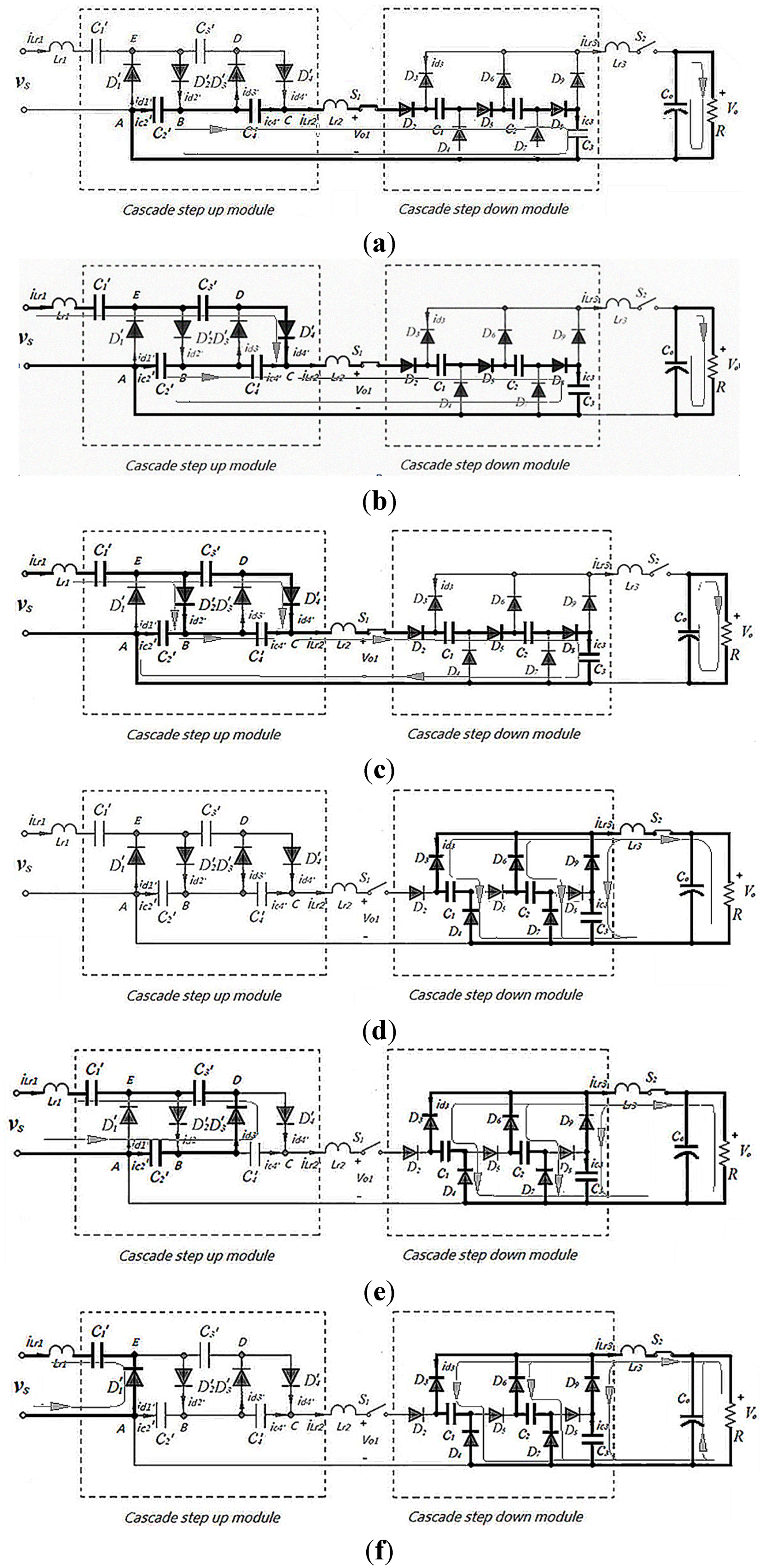
The operation modes and the operation states are shown in
Figure 6. The waveforms of the current and voltage of the proposed circuit are illustrated in
Figure 7.
Figure 6.
The detailed operation states of the proposed circuit: (a) State 1; (b) State 2; (c) State 3; (d) State 4; (e) State 5; and (f) State 6.
Figure 6.
The detailed operation states of the proposed circuit: (a) State 1; (b) State 2; (c) State 3; (d) State 4; (e) State 5; and (f) State 6.
As it can be seen in
Figure 7a, the voltage is firstly stepped up by cascaded step up module to 4
Vs, then is stepped down by the cascaded step down module mentioned above for 4
Vs/3. The input current which is also the current flowing through resonant inductor L
r1 increases slowly and then resonates back to zero in half cycle of the source voltage. Similar operation is found in next half cycle of the source voltage, as shown in
Figure 7b. The voltage amplitudes across the two transistors shown in
Figure 7d are the same and show the difference between the step up voltage
VAC and the output voltage
Vo. Since the circuit is used either to step up or step down, the difference between
VAC and
Vo will not be large, and therefore, the voltage stress is not high.
Figure 7.
Waveform of the current and voltage of the proposed circuit: (a) VAC, Vc1 and Vo; (b) resonant inductor and switched-capacitor voltages and currents; (c) iLr3, ic3, id3; and (d) switch voltages.
Figure 7.
Waveform of the current and voltage of the proposed circuit: (a) VAC, Vc1 and Vo; (b) resonant inductor and switched-capacitor voltages and currents; (c) iLr3, ic3, id3; and (d) switch voltages.
The detailed description of the operation and analysis is as follows. Assume Vssinωt is the source voltage; iLr1, iLr2, iLr3, ic2′, ic4′ id1′, id2′ id3′, id4′, id3, ic3 are the current flowing through the inductors Lr1, Lr2, Lr3, the capacitors C2′, C4′, C3 and the diodes D1′, D2′, D3′, D4′, D3. Lr1, Lr2, Lr3 are the resonant inductors, the capacitances of C1′, C2′ C3′, C4′, C1, C2 and C3 are assumed equal to C.
The steady state operation can be classified into two modes: Mode A, the source is working in the positive half cycle and Mode B, the source is working in the negative half cycle.
- (1)
Mode A (
t0–
t4): S
1 is on and S
2 is off, the circuit is working in the positive half cycle of the source voltage. There are four stages in this period. The circuit is going through state 1 to states 2 and 3 and back to state 1.
- (a)
Stage 1 (
t0–
t1): the circuit is working on state 1. As shown in
Figure 6a, When the sum of source voltage and voltage across C
1′ is smaller than the voltage across C
2′, both D
1′ and D
2′ are reversely biased; when the sum of source voltage, voltage across C
1′ and voltage across C
3′ is smaller than
VAC which is larger than the sum of voltages of the capacitors C
1, C
2 and C
3, then D
3′ and D
4′ are reversely biased, then the currents following through diode L
r1, and D
1′, D
2′, D
3′, and D
4′ are zero, as shown in
Figure 7b, till the sum of source voltage and voltage of capacitors C
1′ and C
3′ is larger than
VAC, Capacitors C
2′ and C
4′ are charging capacitors C
1, C
2 and C
3 in series. The current of the inductor
ic2′ which is equal to
ic4′ and the current of the inductor
iLr2 starts to increase slowly from zero, and the voltages of
vc2′ and
vc4′ are decreasing slowly,
, which is shown in
Figure 7b, then there is:
- (b)
Stage 2 (
t1–
t2): the circuit is working on state 2. As shown in
Figure 6b When the sum of source voltage and voltage across C
1′ is smaller than the voltage across C
2′,both D
1′ and D
2′ are reversely biased; meanwhile, the sum of source voltage and voltages across C
1′, C
3′ is larger than
VAC, and
VAC is equal to the sum of voltage of the capacitors C
1, C
2 and C
3, then the source and the capacitors C
1′ and C
3′ are connected in series and start to charge capacitors C
2′ and C
4′ , and capacitors C
1, C
2, C
3 are now in parallel. The current of the inductor
iLr1 starts to increase slowly from zero, which is equal to the sum of current of the inductor
ic2′ and
iLr1, the voltages of
vc1′ and
vc3′ are decreasing slowly, the voltages of
vc2′ and
vc4′ are increasing,
,
,
,
, which is shown and
Figure 7b, then there is:
- (c)
Stage 3 (
t2–
t3): The circuit is working on state 3. The source voltage is increasing and the sum of source voltage and voltage across C
1′, is larger than the voltage across C
2′, the diode D
2′ is on, the voltage across C
3′ and C
4′ is the same. Then, D
4′ is on. Then, the source voltage and capacitor C
1′ start to charge capacitor C
2′. Meanwhile, Capacitors C
3′ and C
4′ in parallel are charging capacitors C
1, C
2 and C
3 in series, the current of the inductor
iLr1 starts to decrease slowly, and resonant back to zero, which equals the sum of
id2′ and
id4′. The current
id4′ equals
ic4′; the current
id2′ equals the sum of the current flowing through capacitor C
2′ and the capacitor C
4′.
,
,
,
,
,
, as shown in
Figure 6c and
Figure 7b, the equations of operation are:
- (d)
Stage 4 (
t3–
t4): The circuit is working back on state 1. When the source voltage is decreasing and the sum of the source voltage and voltage across C
1′, C
3′ is smaller than
VAC, the sum of source voltage and voltage across C
1′ is smaller than the voltage across C
2′, then all the diodes are reversed, the current following through diodes D
2′ and D
4′ is zero;
VAC is larger than the sum of voltage of the capacitors C
1, C
2 and C
3 because of the resonant inductor, the current of the inductor
iLr2 starts to decrease slowly, and resonates back to zero. The input current
iLr1 is zero, because there is no current flowing through. The capacitors C
2′ and C
4′ start to charge capacitors C
1, C
2 and C
3 in series again, as shown in
Figure 7b. Then:
- (2)
Mode B (t
4–t
8): the switch S
2 is on and S
1 is off. Also, it is working on the negative half cycle. During the entire negative half cycle, the capacitor is parallel and releases energy to load. The current is increasing slowly because of the resonant inductor L
r3, then resonates back to zero at the time instant t
8. The equation of operation is:
The solutions are:
where,
,
,
is the resonant frequency, which is
,
.
is the output voltage. Z
03 is the impedance.
- (a)
Stage 5 (t
4–t
5): The circuit is working on state 4. As shown in
Figure 6d, when sum of source voltage and voltage across C
2′ is smaller than the voltage across C
1′and C
3′, and source voltage is smaller than the voltage across capacitor C
1′, all diodes are reversely biased. There is no current flowing through pre-stage module; all variables are kept constant.
- (b)
Stage 6 (t
5–t
6): The circuit is working on state 5. As shown in
Figure 6e, the sum of source voltage and voltage across C
2′ is larger than the voltage across capacitors C
1′ and C
3′, but the source voltage is still smaller than the voltage across C
1′, source voltage and capacitor C
2′ start to charge capacitors C
1′ and C
3′. The current of the inductor
iLr1 starts to increase slowly, which is equal to the current flowing through capacitor C
2′ and diode D
3′. The voltage across C
2′ is decreasing, the voltages across C
1′ and C
3′ are increasing, till
vc2′ is equal to
vc3′, as shown in
Figure 7b. Hence:
- (c)
Stage 7 (t
6–t
7): The circuit is working on state 6, as shown in
Figure 6f. When the voltage across C
2′ is equal to the voltage across C
3′, which makes diodes D
1′ on and D
3′ off. The source is charging capacitor C
1′, the current of the inductor
iLr1 starts to decrease slowly, and resonates back to zero. The voltage across C
1′ is increasing, Voltages across C
2′, C
3′ and C
4′ keep constant,
, is shown in
Figure 7b. Then:
- (d)
Stage 8 (t
7–t
8): The circuit is working back on state 4. When the source voltage is decreasing and the sum of source voltage and voltage across C
2′, is smaller than the voltage across C
1′ and C
3′, source voltage is smaller than the voltage across capacitor C
1′, all diodes are reversely biased. There is no current flowing through the pre-stage module; all the variables are kept constant, as shown in
Figure 7b.
All the differential equations can be solved by a numerical method according to the boundary conditions.
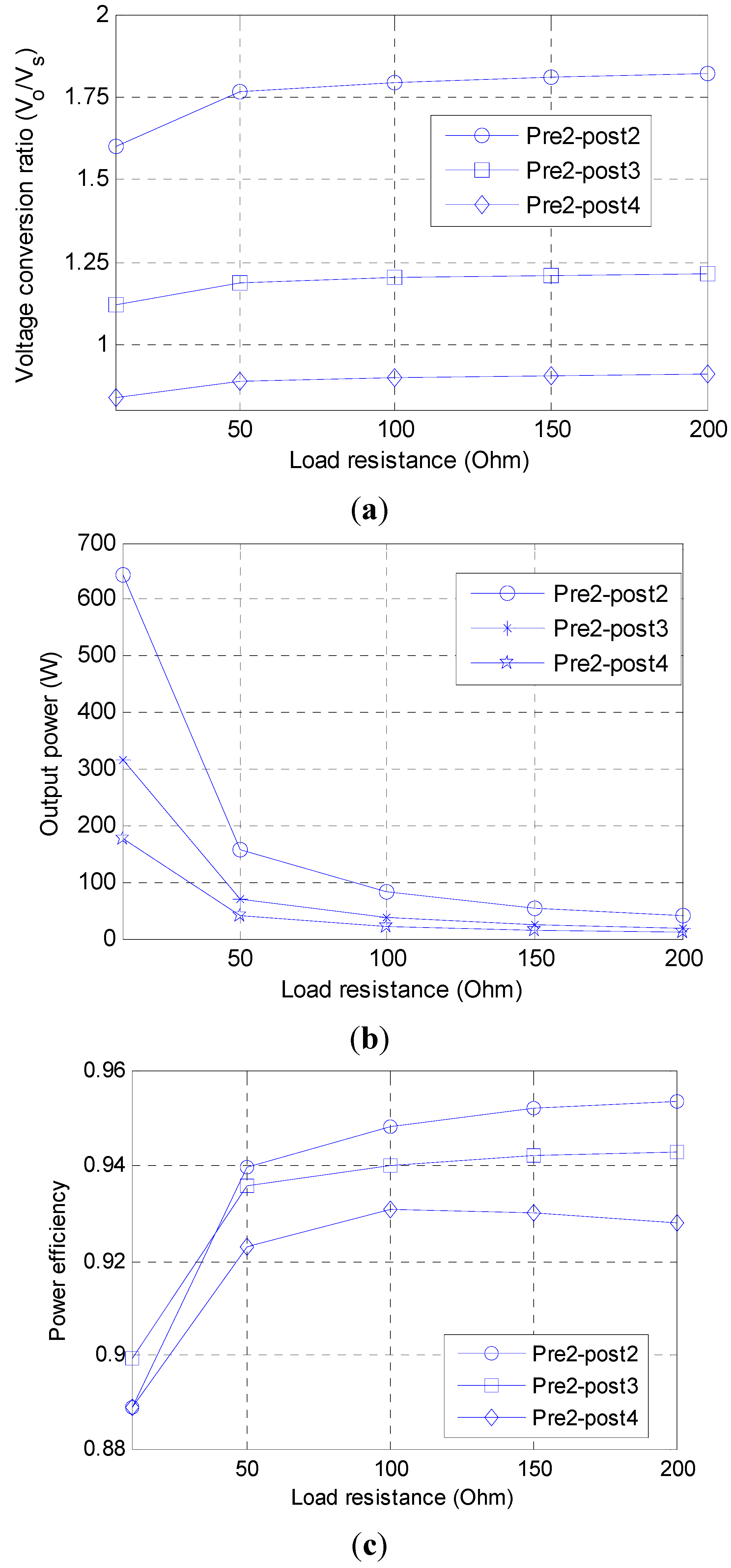
3.4. Performance of Different Step Up/Down Cascades
The study of different combinations of cascade modules
n = 2, 3, 4 pre-step-up-stage and
m = 2, 3, 4 post-step-down-stage of the circuits has been carried out by PSIM9.0 to verify the concept of the proposed circuit. As shown in
Figure 8 and
Figure 9, the voltage conversion ratio, the output power, and the power efficiency for different cascades module have been presented.
As we can see in
Figure 8, the conversion ratio, output power and power efficiency are decreasing with the step down stage increasing. In a fixed stage circuit, for example,
n = 2 step-up cascades and
m = 3 step-down cascades, the output power decreases quickly, meanwhile, the conversion ratio and the power efficiency increase quickly when the load resistance increases from 0 Ω to 50 Ω. Output power decreased slowly and stably. Meanwhile, the voltage conversion ratio and the power efficiency increased slowly and stably when the load resistor is increasing from 50 Ω to 200 Ω. Vice versa, the conversion ratio, output power and power efficiency are increasing with the pre-stage (step up stage) increasing. The more step-up cascades, the more quickly output power decreased; the conversion ratio and the power efficiency increase quickly when the load resistance increases from 0 Ω to 50 Ω. As it can be seen, when there is only one step-up cascade, the voltage conversion ratio, the output power, the power efficiency all changed more slowly than 2 and 3 step-up cascades. Output power decreases slowly and stably. Meanwhile, the voltage conversion ratio and the power efficiency increase slowly and stably when the load resistor is increasing from 50 Ω to 200 Ω. To conclude, the proposed circuit works stably when the power is below 170 W.
Figure 8.
The output power, voltage conversion ratio and power efficiency versus load resistor of n = 2 to pre-stage, m = 2, 3, 4 to post-stage: (a) voltage conversion ratio versus load resistor; (b) output power versus load resistor; and (c) the power efficiency versus output current.
Figure 8.
The output power, voltage conversion ratio and power efficiency versus load resistor of n = 2 to pre-stage, m = 2, 3, 4 to post-stage: (a) voltage conversion ratio versus load resistor; (b) output power versus load resistor; and (c) the power efficiency versus output current.
The simulation result also shows the power efficiency is above 90% and either pre-stage or post- stage increases will induce the decrease in power efficiency.
Figure 9.
The output power, voltage conversion ratio and power efficiency versus load resistor of n = 1, 2, 3 to pre-stage, m = 3 to post-stage: (a) the output power versus load resistor; (b) conversion ratio versus load resistor; and (c) the power efficiency versus output current of 1, 2, 3 pre-stage, 3 post-stage.
4. Experimental Results
The performance of the proposed circuit is verified by the experiment. An
n = 2 to pre-stage,
m = 3 to post-stage circuit is built to verify the performance of the circuit. The waveform of the input voltage, output voltage, input current, resonant inductor current, power efficiency, and the power
versus different loads are shown in
Figure 10,
Figure 11 and
Figure 12. The power source is emulated by a signal generator and a high frequency amplifier which is programed to 50 kHz and 50 V in amplitude. The high frequency AC source is now a new wind generator for distributed power generation because they are usually smaller size and low power and are used by the public as high frequency and small sized generators. The value of the step down switching capacitor is 6.8 µF, the capacitance of the voltage multiplier is also 6.8 µF.
Figure 10.
The waveform of switched signal, input and output voltage, input current (load resistance is 200 Ω): (a) Ch1: input voltage (40 V/div); Ch2: switched signal S1 (20 V/div); Ch3: switched signal S2 (10 V/div); (b) Ch1: stepped up voltage Vo1 (100 V/div); Ch2: input voltage (100 V/div); Ch4: output voltage (100 V/div); and (c) Ch1: output voltage (100 V/div); Ch2: input voltage (100 V/div); Ch4: input current (2 A/div).
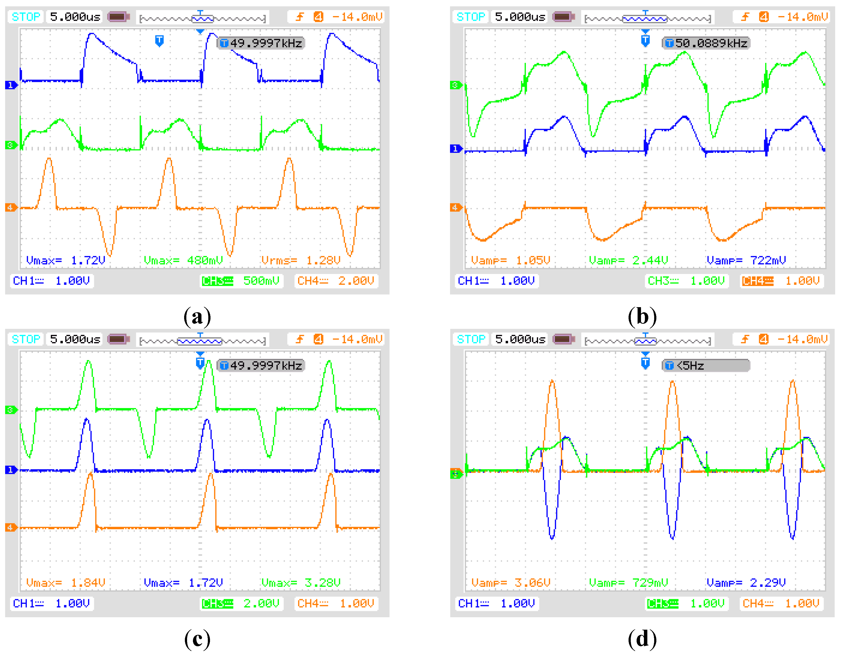
Figure 11.
The waveform of current flowing through resonant inductor, diode and capacitor (load resistance is 100 Ω). (a) Ch1: inductor current iLr3 (1 A/div); Ch3: inductor current iLr2 (500 mA/div); Ch4: iLr1 (2 A/div); (b) Ch1: inductor current iLr2 (1 A/div); Ch3: current flowing through C3 (1 A/div); Ch4: current flowing through D3 (1 A/div); (c) Ch1: current flowing through D4′ (1 A/div); Ch3: inductor current iLr1 (2 A/div); Ch4: current flowing through D2′ (1 A/div); (d) Ch1: current flowing through C4′ (1 A/div); Ch3: inductor current iLr1 (1 A/div); Ch4: current flowing through D4′ (1 A/div).
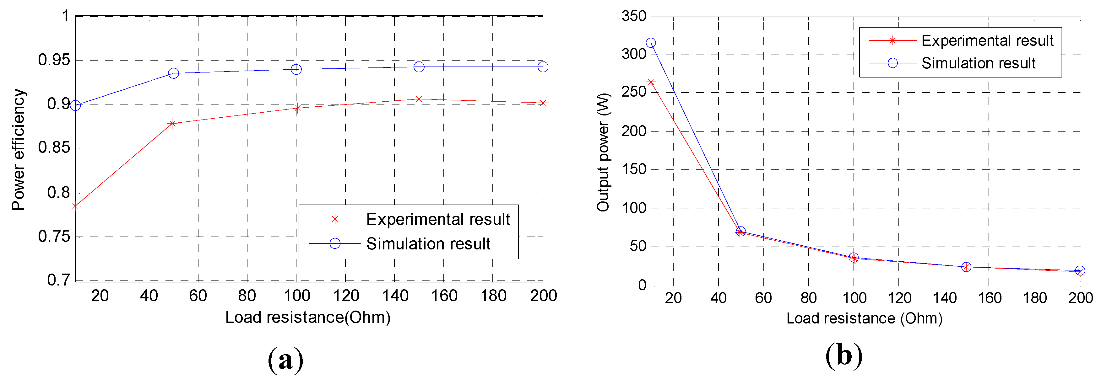
Figure 12.
Simulation and experimental results for power efficiency and output power of the proposed circuit: (a) simulation and experimental results for power efficiency; and (b) simulation and experimental results for output power.
Figure 12.
Simulation and experimental results for power efficiency and output power of the proposed circuit: (a) simulation and experimental results for power efficiency; and (b) simulation and experimental results for output power.
The resonant inductors L
r1, L
r2 are designed to be 3.5 µH and 1.5 µH, respectively. However, in the experiment, the resonant inductor is realized by the parasitic inductor of the capacitors to achieve ZCS; the output capacitor is 47 µF. The load resistor is variable. Therefore, the circuit is very simple. The specifications and part number are illustrated in
Table 1.
Table 1.
Specification of the proposed circuit.
Table 1.
Specification of the proposed circuit.
| Parameter | Symbol | Specified values |
|---|
| Input voltage | Vs | 50 kHz, 50 V |
| Switching frequency | fs | 50 kHz |
| Output voltage | Vo | DC 60 V |
| Power | Po | 100 W |
| Mosfet | S1, S2 | IRF640 |
| Diode 2–9 | D2’-D4’, D2-D9 | MBR20100 |
| Diode 1 | D1’ | MBR20200 |
| All capacitors | C1’-C4’, C0-C3 | 6.8 μF |
Figure 10 and
Figure 11 show the waveform of the input voltage, output voltage, input current, resonant inductor current and current flowing through the diodes, respectively, when the load resistance is 200 Ω.
Figure 10 shows the switched signal and input output voltage and current.
Figure 10a shows the control signal is a pair of complementary signals and is easy to achieve. As it can be seen, the switch S
1 is on when the input voltage is working on the positive half wave, the switch S
2 is on when the input voltage in working on negative half cycle. In
Figure 10b,c the input voltage, stepped up voltage, output voltage, and input current are displayed, which shows that the input voltage is first stepped up to 180 V, then stepped down to 61.2 V, which confirms the concept and the performance of the proposed circuit.
Figure 10c shows the input and output voltages. In the half cycle, the current is increasing from zero and resonate back to zero again because of the resonant inductors, and the input voltage is converted by 2 × n/mV
s,
i.e., 2 × 2/3 V
s.
Figure 11 shows the current flowing through the component of diodes, capacitors and inductors. In
Figure 11a, it shows the current flowing through the resonant inductor L
r1, L
r2 and L
r3. The introduced resonant inductors reduce the current spikes, which reduce the current pressure of the components and extend their life. Meanwhile, it keeps the MOSFETs turning on and off at zero current, and ZCS is achieved.
Figure 11b shows the current flowing through inductor L
r2, capacitor C
3 and diode D
3. It shows that the switches and diodes are working on ZCS.
Figure 11c shows that current flowing through D
4′, D
2′ and inductor current
iLr1. According to
Figure 11d, the input current is equal to the sum of currents flowing through diodes D
4′, D
2′, and it also shows that the diode D
4′conducts first and then diode D
4′ conducts. Meanwhile, the inductor current
iLr1 is equal to the sum of current flowing through capacitor C
4′ and the diode D
4′. There is a slight difference between simulation result and experiment result as compared with
Figure 7b. The current in experiment as shown in
Figure 11c is a resonant current because the resonant inductor in experiment is the parasitic inductor which exists in each capacitor.
Figure 12 shows the measured and simulated power efficiency and output power
versus the load resistor. In
Figure 12a, the simulation power efficiency of the proposed circuit is high, up to 94%, and the experimental result is around 90%. Due to the power loss of the switches, the diodes, and the wires, the power efficiency decreased quickly when the load resistor decreased, especially in the experiment.
That is also because that at light load, the power loss in the circuit is mainly due to the diodes, which experience the forward bias voltage drop and conducting loss of the transistors. Therefore, power efficiency decreases significantly. At heavy load, switching loss is the major loss of the power converter. However, soft switching technique is introduced to reduce the switching loss. Other methods including switches with small on resistance, diodes with low forward bias voltage and inductors with lager inductance can also improve the efficiency. The simulation result agree well with the above theory, however, in the experimental result, conduction loss is mostly the main part of the total loss that is because the more step up/down stages, the more conduction loss account. The output power is shown in
Figure 12b. The output power is over 300 W in the simulation result and is 270 W in the experimental result. The output power decreased quickly when the load resistor increased to 50 Ω, and then decreased slowly. Therefore, the suggested power will be limited to 100 W and lower. Also, the power efficiency will be higher compared with
Figure 12a.


