1. Introduction
The harmonic pollution affects all domestic and industrial grids. No modern environment such as computers, servers, air conditioners, speed controllers
etc. can escape this equipment pollution. All these so called “non-linear” loads seriously affect the quality of the grid current and voltage [
1,
2].
The different current disturbance identification methods can be classified into two families. The first one, in the frequency domain, is based on the use of a Fast Fourier Transform (FFT) to extract the current harmonics. This method is well suited for loads where the harmonic content varies slowly. It also offers the advantage of selecting individual harmonics and compensating the most dominant harmonic. It should be pointed out that this method is too time consuming because of all the required real-time transformations for the extraction of harmonics.
The second family, in the time domain, is based on the computation of instantaneous power. The method of instantaneous active and reactive power was developed in many applications [
1,
2,
3,
4]. But the disadvantage is that it gives correct results only for a healthy grid,
i.e., balanced and undistorted voltage [
5,
6].
The principle of DPC for Pulse Width Modulation (PWM) converters was proposed for the first time in 1986 [
7] and developed later for other many applications. The DPC purpose essentially was to remove both the PWM modulator and the internal regulation loops by replacing them by a predetermined switching table. The first DPC control type configuration has been proposed in [
8], for the direct control of instantaneous active and reactive power of three-phase PWM rectifiers without grid voltage sensors. Based on this approach, many studies have been developed for different power topologies. The common objective of these studies was to ensure sinusoidal currents and a unity power factor with a decoupled control of active and reactive power [
9].
The standard DPC requires zero reactive power reference, while the active power reference is calculated from the Direct Current (DC) bus controller output [
10]. This paper proposes a DPC technique, which in contrast to standard implementation, requires zero active and reactive power disturbance references for rejecting any disturbance due to harmonics [
11,
12]. That is why it is called Zero DPC or ZDPC. This paper presents the proposed ZDPC method.
It is organized as follows;
Section 2 presents the principle of the standard DPC.
Section 3 deals with the detailed operation principle of the proposed ZDPC method. In
Section 4, simulation results under different conditions (balanced, unbalanced, distorted grid voltage) are presented and compared to standard DPC [
10]. Finally, in
Section 5, we present the experimental validation of the proposed method. Then we conclude the paper.
2. Principle of Standard DPC
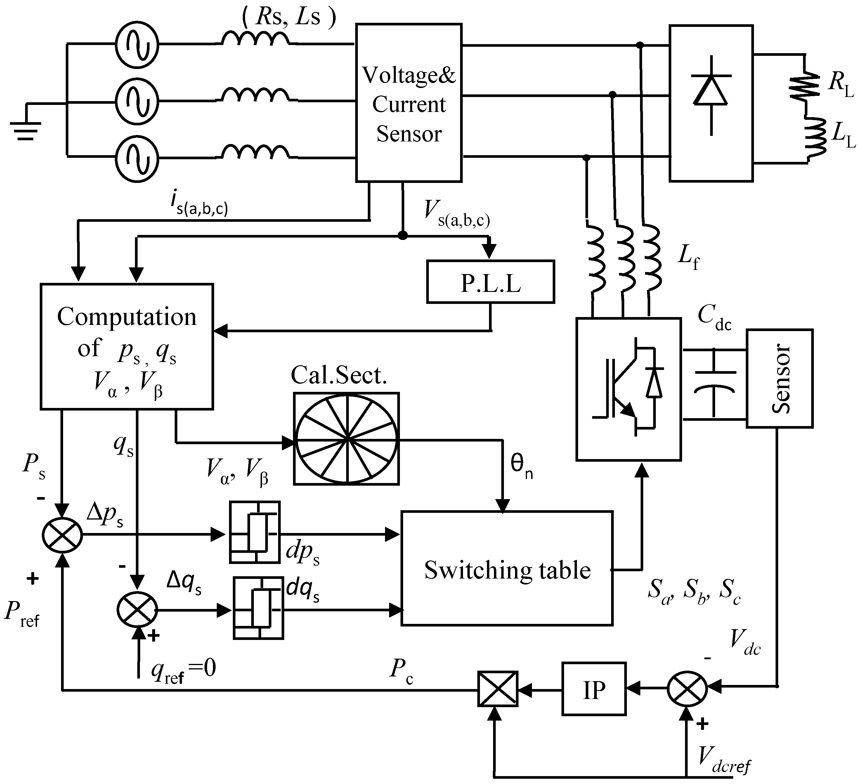
The block scheme in
Figure 1 shows the standard DPC configuration where the zero reactive power
qref and active power
pref reference (delivered from the DC bus voltage controller) are compared with the calculated
ps and
qs values given respectively by Equations (1) and (2), by means of two level hysteresis controllers [
9,
13,
14,
15]:
where
ps(
t) and
qs(
t) are the instantaneous real and imaginary source power.
Figure 1.
Standard DPC control block diagram.
Figure 1.
Standard DPC control block diagram.
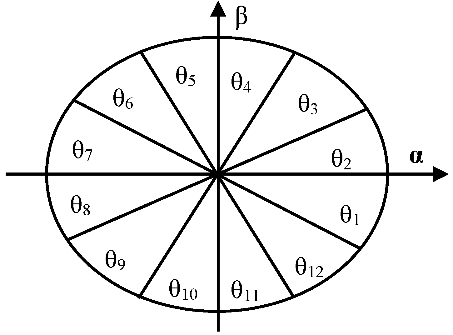
2.1. The Sector Choice
The digitized variables d
ps, d
qs and grid voltage vector position θ (Equation (3)), form a digital word, for access to the address of switching table to select the appropriate control voltage vector:
For this purpose, the stationary coordinates are divided into 12 sectors, as shown in
Figure 2, and the sectors can be numerically expressed as [
9,
13,
14,
16]. The digitized signal errors d
ps, d
qs and voltage phase θ
n are the inputs of switching table shown in
Table 1 whose output is the switching state (S
a, S
b, S
c) of the converter. By using this switching table, the optimal state of the converter can be selected uniquely during each time interval according to combination of the table inputs. The selection of the optimal switching state is performed so that the power errors can be restricted within the hysteresis bands.
Figure 2.
(α, β) sectors representation.
Figure 2.
(α, β) sectors representation.
Table 1.
ZDPC switching table.
Table 1.
ZDPC switching table.
| dp | dq | θ1 | θ2 | θ3 | θ4 | θ5 | θ6 | θ7 | θ8 | θ9 | θ10 | θ11 | θ12 |
|---|
| 1 | 0 | v6 | v7 | v1 | v0 | v2 | v7 | v3 | v0 | v4 | v7 | v5 | v0 |
| 1 | v7 | v7 | v0 | v0 | v7 | v7 | v0 | v0 | v7 | v7 | v0 | v0 |
| 0 | 0 | v6 | v1 | v1 | v2 | v2 | v3 | v3 | v4 | v4 | v5 | v5 | v6 |
| 1 | v1 | v2 | v2 | v3 | v3 | v4 | v4 | v5 | v5 | v6 | v6 | v1 |
2.2. Hysteresis Controller
The main idea of the DPC method is to maintain the instantaneous active and reactive power within a desired band. This control is based on two hysteresis comparators whose input is the error between the reference and estimated values of the active and reactive power [
9,
13], given by Equations (5) and (6), respectively:
The hysteresis comparators are used to provide two logic outputs d
ps and d
qs. The state “1” corresponds to an increase of the controlled variable (
ps and
qs) while “0” corresponds to a decrease, following Equations (7) and (8):
where
hp and
hq are the hysteresis bands.
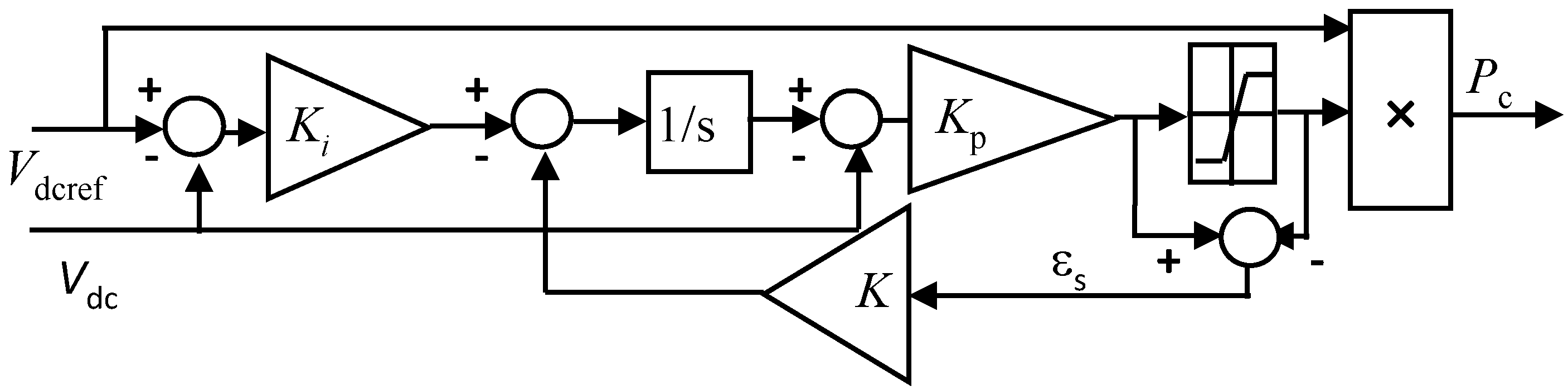
2.3. PI Controller
The DPC method must provide regulation of the DC bus to maintain the capacitor voltage around the voltage reference (
Vdcref). For this purpose a PI controller is generally used [
13].
Figure 3 shows the simulation model of the controller.
Figure 3.
Simulation model of IP controller.
Figure 3.
Simulation model of IP controller.
The values of proportional and integral gains, K
p and K
i, are given respectively by the Equations (9) and (10):
where
: damping coefficient (
,
: natural pulsation and
K: anti-windup gain.
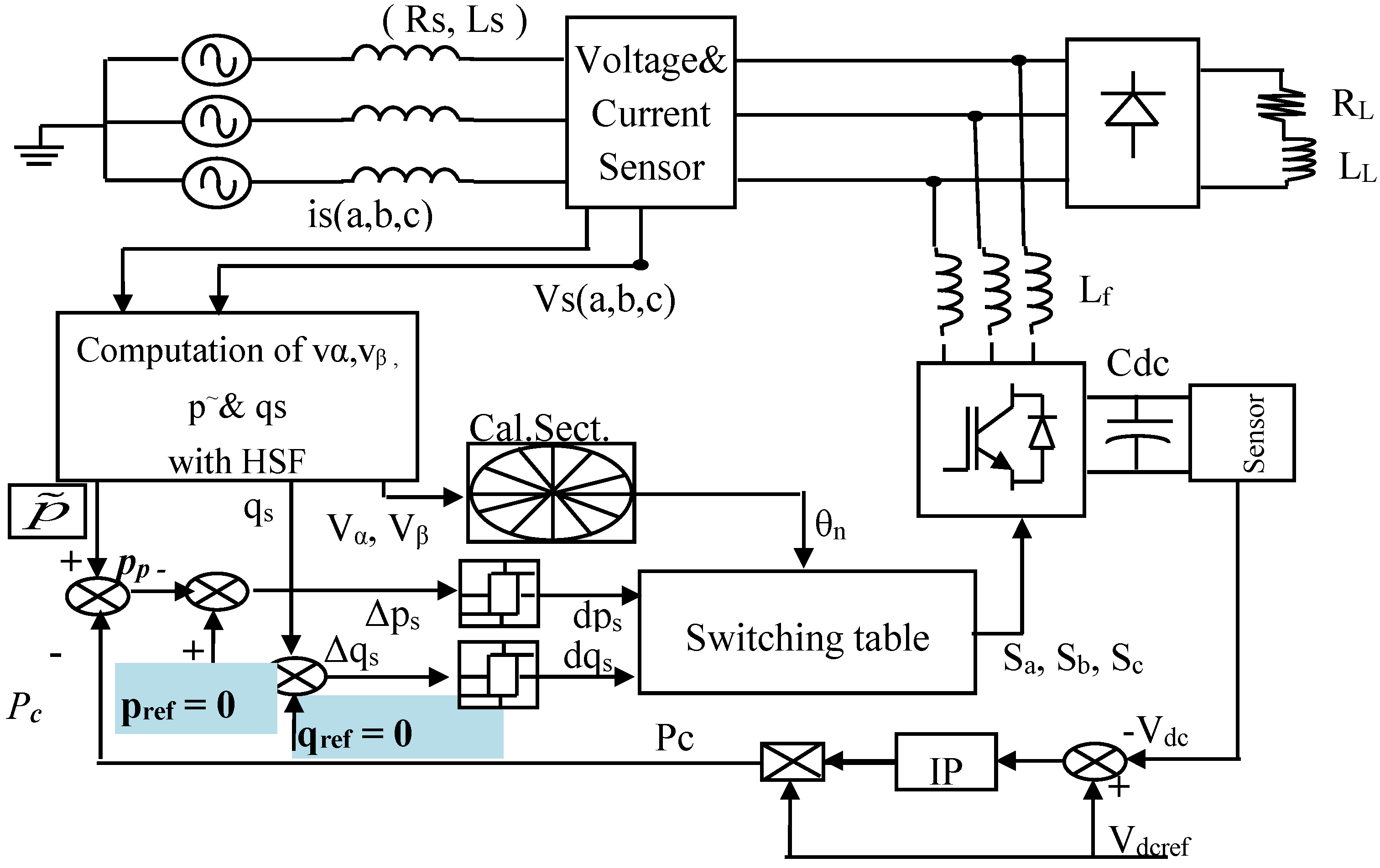
3. Principle of the Proposed ZDPC
Figure 4 shows the structure of the proposed ZDPC. In this control strategy, the active and reactive power disturbance references are set to zero [
11,
12]. We note that in this structure the phase locked loop (PLL) is no longer needed. The HSF filter is used to separate the fundamental and harmonic components of the line currents and voltages to perform the power compensation (
Figure 5).
Figure 4.
ZDPC Shunt Active Power Filter Synoptic.
Figure 4.
ZDPC Shunt Active Power Filter Synoptic.
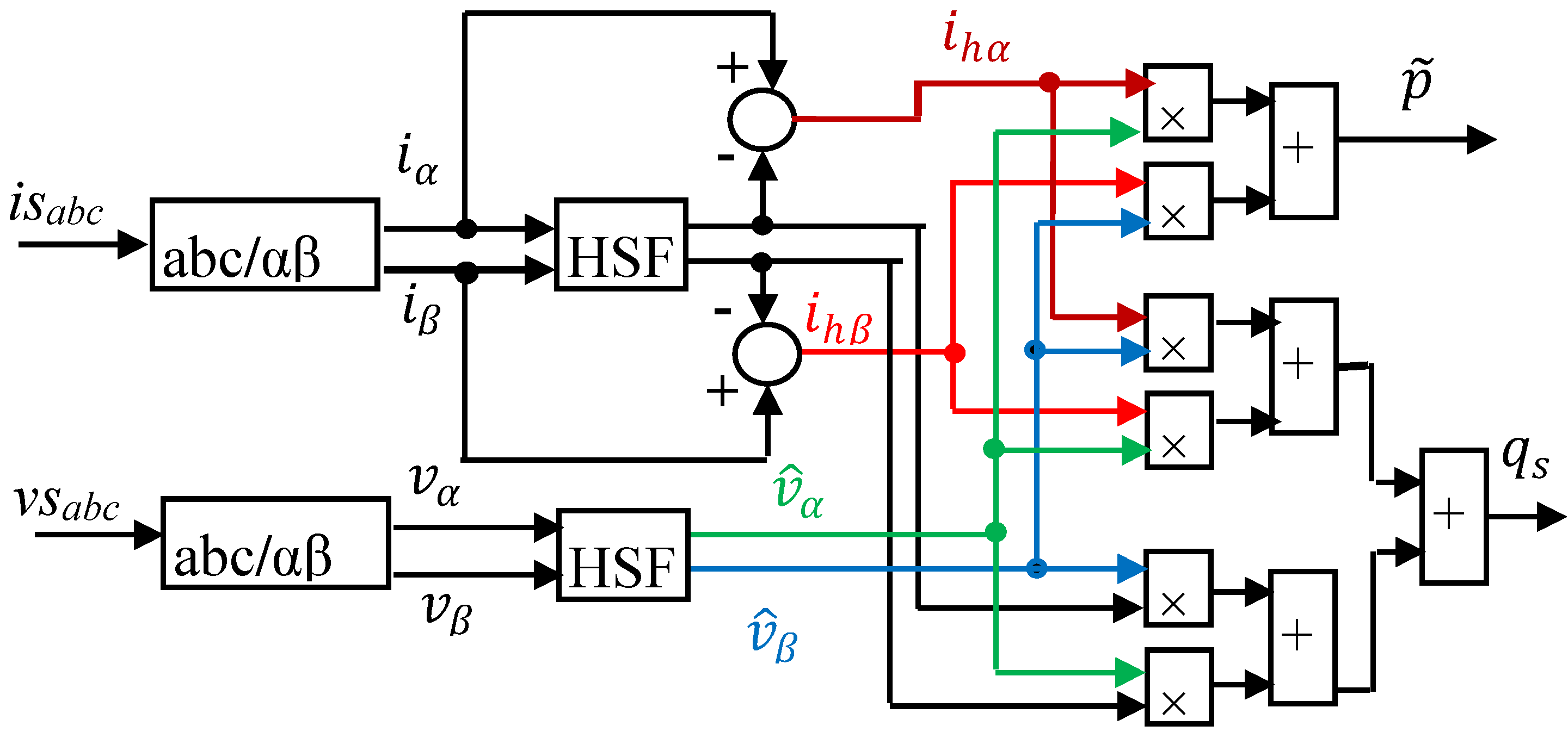
Figure 5.
Computation of vα, vβ,
& qs with HSF.
Figure 5.
Computation of vα, vβ,
& qs with HSF.
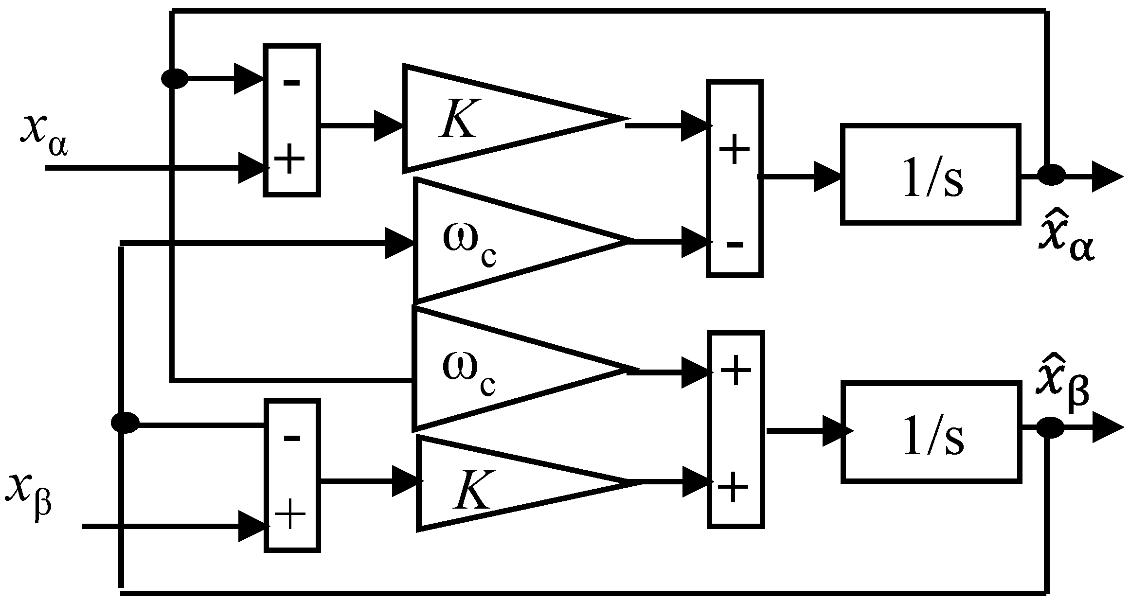
3.1. The HSF Filter
To improve the performance of the conventional instantaneous power method, the HSF has been implemented, for extracting the fundamental component of the current and voltage in the synchronous frame without phase shifting or amplitude errors [
17]. The block diagram of HSF is shown in
Figure 6.
Figure 6.
Block diagram of HSF filter.
Figure 6.
Block diagram of HSF filter.
The transfer function of the filter can be expressed as follows [
13]:
From the transfer Equation (11), we get:
where the quantities
and
xαβ represent the output and input of the filter, respectively. They may be either
vαβ or
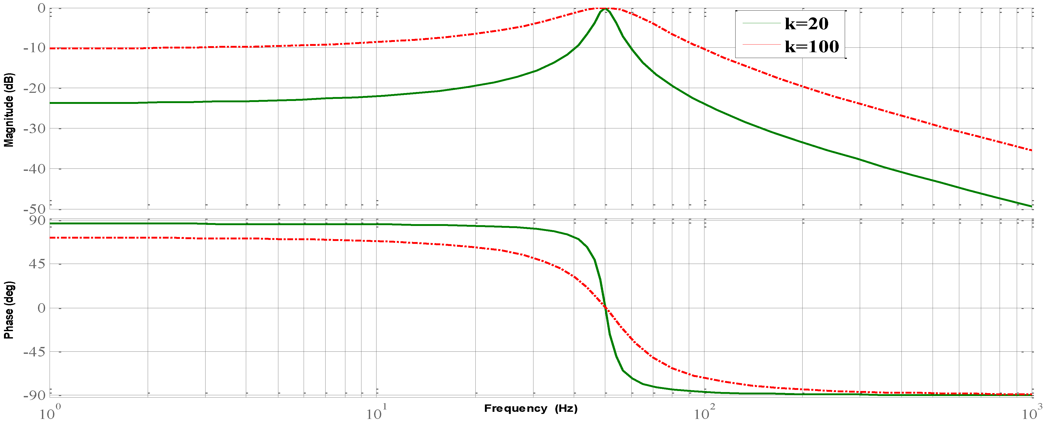
iαβ. We note that for pulsation ω = ω
c, the phase shift introduced by the filter is zero and the gain is unity. We also observe that K value decrease improves the selectivity of HSF (
Figure 7), we chose
K = 20.
Figure 7.
Bode plot of HSF filter.
Figure 7.
Bode plot of HSF filter.
From the HSF output, the ac component of active instantaneous power can be obtained by Equation (14) [
18]:
with
ihα and
ihβ given respectively by Equations (15) and (16):
where the terms
ihα and
ihβ are the harmonic components in αβ axis. Meanwhile, the instantaneous reactive power is defined by:
3.2. Generation of Control Vector
Adding the AC component
of the instantaneous active power, related to both current and voltage disturbances, to the active power
pc, necessary for the dc bus regulation, we obtain the active power disturbance
pp which can be can be expressed as:
To compensate the active and reactive power (
pp and
qs) disturbances, a comparison with their zero reference is done. The comparison results go through a hysteresis block that generates d
ps and d
qs. Depending on the selected sector (θ
n) and (d
ps, d
qs), the appropriate control vector (S
a, S
b, S
c) is produced by using the switching table (
Table 1).
4. Simulation Results
To achieve the simulation of ZDPC technique, a model in Matlab/SIMULINK frame and SimPower-Systems Block set, R2008b, Mathworks, USA, 2008, is developed. To compare the results obtained to those given by [
10], the same system parameters specified in [
10] and in the
Appendix have been used. The simulation is conducted for different grid voltage source conditions:
Case A: balanced sinusoidal grid voltage.
Case B: unbalanced sinusoidal grid voltage.
Case C: balanced distorted grid voltage.
Case D: unbalanced and distorted grid voltage.
4.1. Standard DPC Simulation
Table 2.
Grid voltage, load current and THDs under different grid voltage conditions.
Table 2.
Grid voltage, load current and THDs under different grid voltage conditions.
| Case | Source voltage | Load current |
|---|
| vsa | vsb | vsc | iLa | iLb | iLc |
|---|
| rms (v) | THD (%) | rms (v) | THD (%) | rms (v) | THD (%) | rms (A) | THD (%) | rms (A) | THD (%) | rms (A) | THD (%) |
|---|
| A | 220 | 0.61 | 220 | 0.61 | 220 | 0.61 | 15.33 | 28.58 | 15.33 | 28.58 | 15.33 | 28.58 |
| B | 220 | 0.61 | 180 | 0.80 | 138 | 1.18 | 13.85 | 22.98 | 12.73 | 28.57 | 11.00 | 35.74 |
| C | 220 | 12.83 | 220 | 12.83 | 220 | 12.83 | 14.98 | 29.69 | 15.32 | 29.03 | 15.71 | 28.65 |
| D | 220 | 12.82 | 180 | 15.72 | 140 | 20.52 | 13.64 | 23.41 | 12.22 | 31.98 | 11.65 | 33.70 |
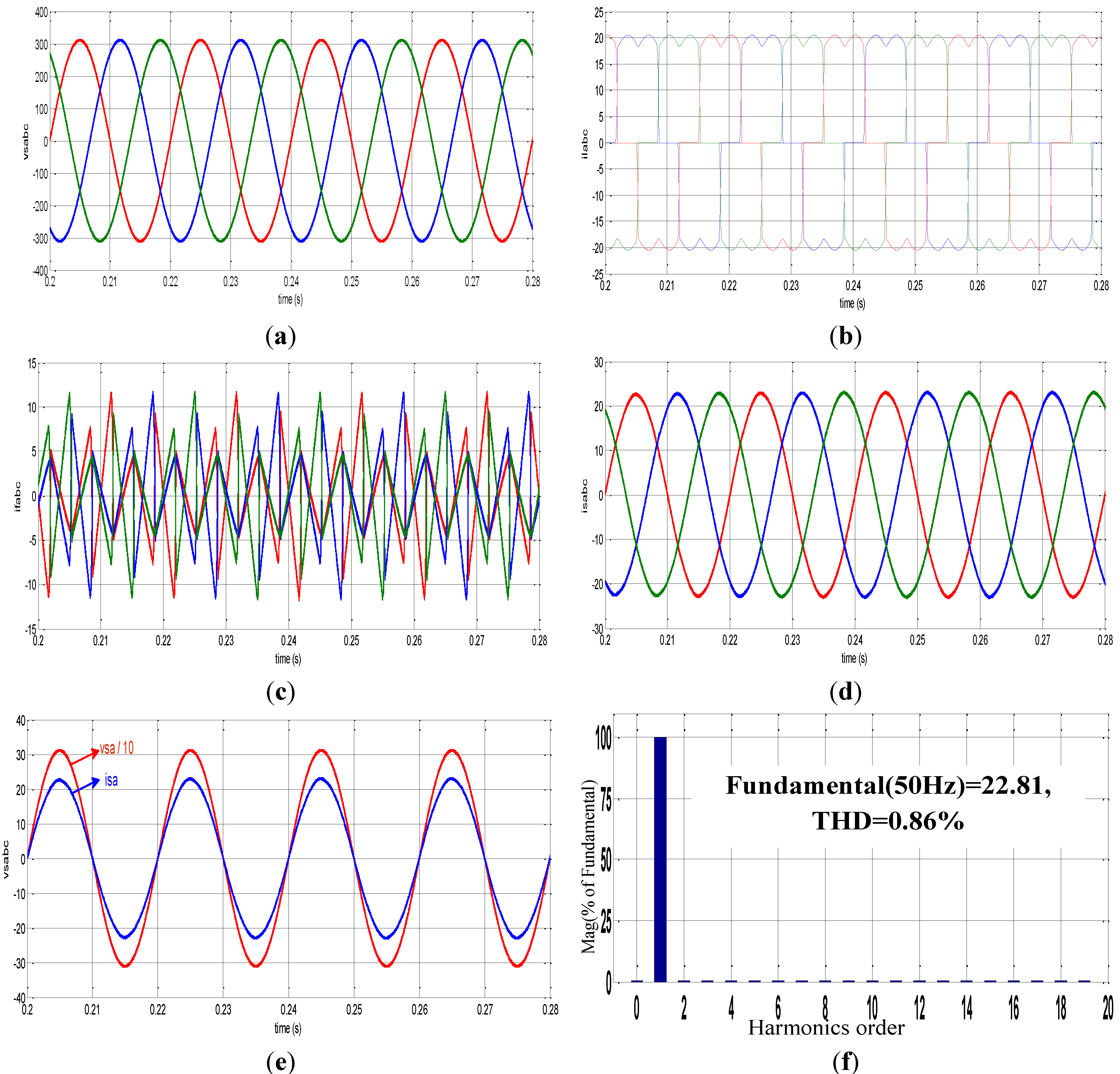
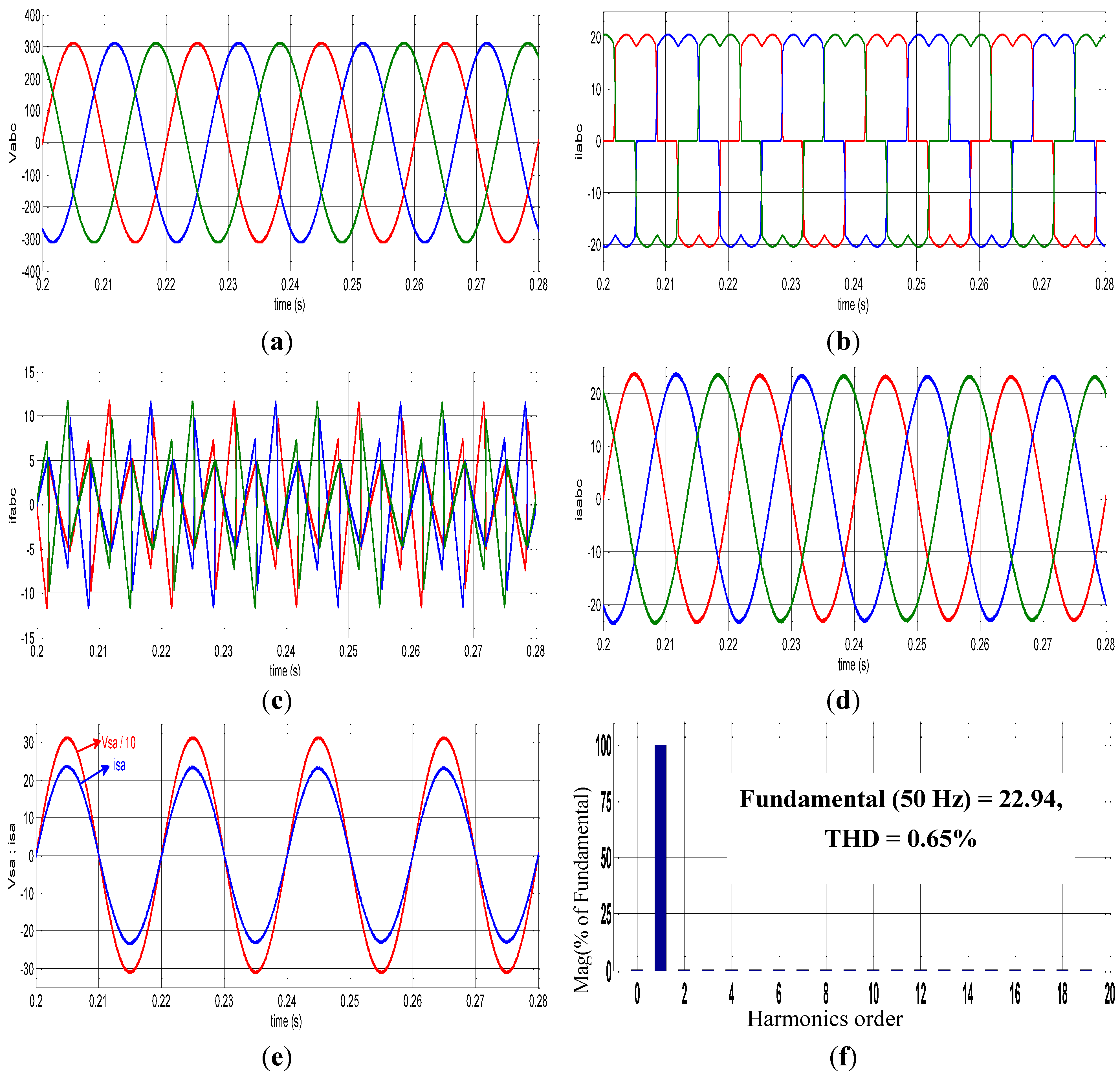
4.1.1. Case A: Balanced Sinusoidal Grid Voltage
The results are shown in
Figure 8, and summarized in
Table 3. We observe a good compensation for the line current, with a THD is = 0.86% reduced below the standard IEEE-519.
Table 3.
Simulation results for DPC and ZDPC strategies under different grid conditions (A, B, C, D).
Table 3.
Simulation results for DPC and ZDPC strategies under different grid conditions (A, B, C, D).
| Case | Control strategies | Source currents | Filter currents |
|---|
| isa | isb | isc | ifa | ifc | ifb |
|---|
| rms (A) | THD (%) | rms (A) | THD (%) | rms (A) | THD (%) | rms (A) | rms (A) | rms (A) |
|---|
| A | DPC | 16.13 | 0.86 | 16.14 | 0.87 | 16.14 | 0.87 | 4.66 | 4.66 | 4.66 |
| ZDPC | 16.22 | 0.65 | 16.22 | 0.69 | 16.22 | 0.66 | 4.65 | 4.65 | 4.65 |
| B | DPC | 14.22 | 12.48 | 13.57 | 15.80 | 13.15 | 11.35 | 2.73 | 4.55 | 4.38 |
| ZDPC | 13.75 | 1.24 | 13.49 | 1.22 | 13.75 | 0.98 | 3.27 | 4.57 | 4.84 |
| C | DPC | 16.23 | 6.09 | 16.07 | 6.58 | 16.21 | 6.47 | 4.99 | 4.55 | 4.56 |
| ZDPC | 16.26 | 0.72 | 16.16 | 0.72 | 16.22 | 0.76 | 4.82 | 4.60 | 4.74 |
| D | DPC | 14.30 | 6.25 | 13.04 | 11.59 | 13.40 | 10.24 | 3.42 | 4.4 | 4.52 |
| ZDPC | 13.81 | 1.48 | 13.52 | 1.53 | 13.81 | 1.22 | 3.32 | 4.75 | 4.53 |
Figure 8.
Simulation results for balanced sinusoidal grid voltage: (a) three-phase line voltages; (b) three-phase load currents; (c) three-phase filter currents; (d) three-phase line currents; (e) line voltage and current, phase-a; (f) frequency spectrum of line current, phase-a.
Figure 8.
Simulation results for balanced sinusoidal grid voltage: (a) three-phase line voltages; (b) three-phase load currents; (c) three-phase filter currents; (d) three-phase line currents; (e) line voltage and current, phase-a; (f) frequency spectrum of line current, phase-a.
4.1.2. Case B: Unbalanced Sinusoidal Grid Voltage
For this case, the phase-b is unbalanced (
va = 220 V,
vb = 180 V,
vc = 140 V), which gives a Total Unbalance (TUv = 22.2%).
Figure 9 and
Table 3 show the results; compensation of line currents is low (THDis = 12.48%, TUis = 4.20% and TUil = 10.37%).
Figure 9.
Simulation results for unbalanced sinusoidal grid voltage: (a) three-phase line voltages; (b) three-phase load currents; (c) three-phase filter currents; (d) three-phase line currents; (e) line voltage and current, phase-a; (f) frequency spectrum of line current, phase-a.
Figure 9.
Simulation results for unbalanced sinusoidal grid voltage: (a) three-phase line voltages; (b) three-phase load currents; (c) three-phase filter currents; (d) three-phase line currents; (e) line voltage and current, phase-a; (f) frequency spectrum of line current, phase-a.
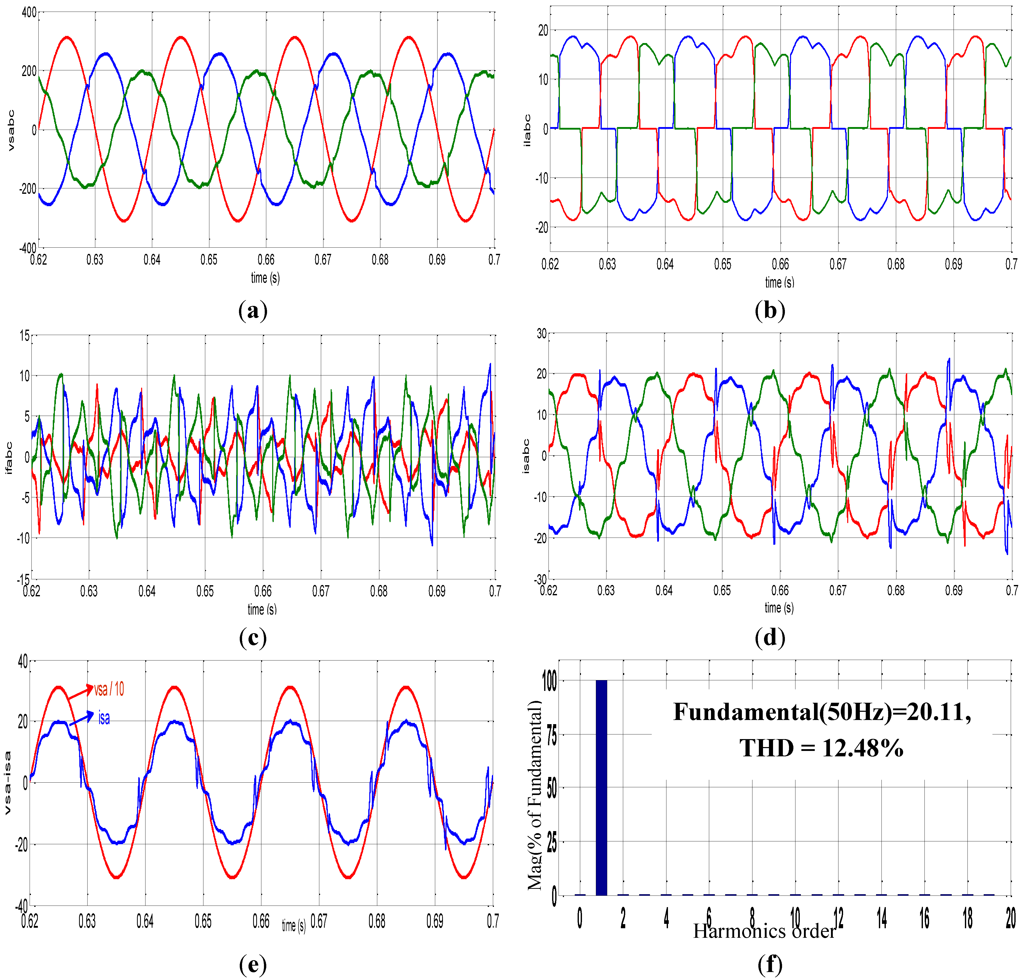
4.1.3. Case C: Balanced Distorted Grid Voltage
In this case the grid voltage is balanced but is distorted with a THDv = 12.83% as shown in
Table 2. The simulation results are shown in
Figure 10, where we observe a low compensation line current (THDis = 6.09%) for the three phases. Summary of the results is given in
Table 3.
Figure 10.
Simulation results of balanced distorted grid voltage: (a) three-phase line voltages; (b) three-phase load currents; (c) three-phase filter currents; (d) three-phase line currents; (e) line voltage and current, phase-a; (f) frequency spectrum of line current, phase-a.
Figure 10.
Simulation results of balanced distorted grid voltage: (a) three-phase line voltages; (b) three-phase load currents; (c) three-phase filter currents; (d) three-phase line currents; (e) line voltage and current, phase-a; (f) frequency spectrum of line current, phase-a.
4.1.4. Case D: Unbalanced and Distorted Grid Voltage
This is the worst case, as it is shown in
Figure 11 and
Table 2. The simulation results are shown in
Figure 11 and
Table 3. Compensation of line current is low (THDis = 6.25%, TUis = 5.07% and TUil = 8.43%).
Figure 11.
Simulation results for unbalanced distorted grid voltage: (a) three-phase line voltages; (b) three-phase load currents; (c) three-phase filter currents; (d) three-phase line currents; (e) line voltage and current, phase-a; (f) frequency spectrum of line current, phase-a.
Figure 11.
Simulation results for unbalanced distorted grid voltage: (a) three-phase line voltages; (b) three-phase load currents; (c) three-phase filter currents; (d) three-phase line currents; (e) line voltage and current, phase-a; (f) frequency spectrum of line current, phase-a.
4.2. ZDPC Simulation
4.2.1. Case A: Balanced Sinusoidal Grid Voltage
The results are shown in
Figure 12. It is observed that there is a good compensation for the line current, and the THD is reduced below the standard IEEE-519 (THDis = 0.65%).
Table 3 presents the comparison between standard DPC and ZDPC. One can observe that both techniques give nearly the same results.
Figure 12.
Simulation results for balanced sinusoidal grid voltage: (a) three-phase line voltages; (b) three-phase load currents; (c) three-phase filter currents; (d) three-phase line currents; (e) line voltage and current, phase-a; (f) frequency spectrum of line current, phase-a.
Figure 12.
Simulation results for balanced sinusoidal grid voltage: (a) three-phase line voltages; (b) three-phase load currents; (c) three-phase filter currents; (d) three-phase line currents; (e) line voltage and current, phase-a; (f) frequency spectrum of line current, phase-a.
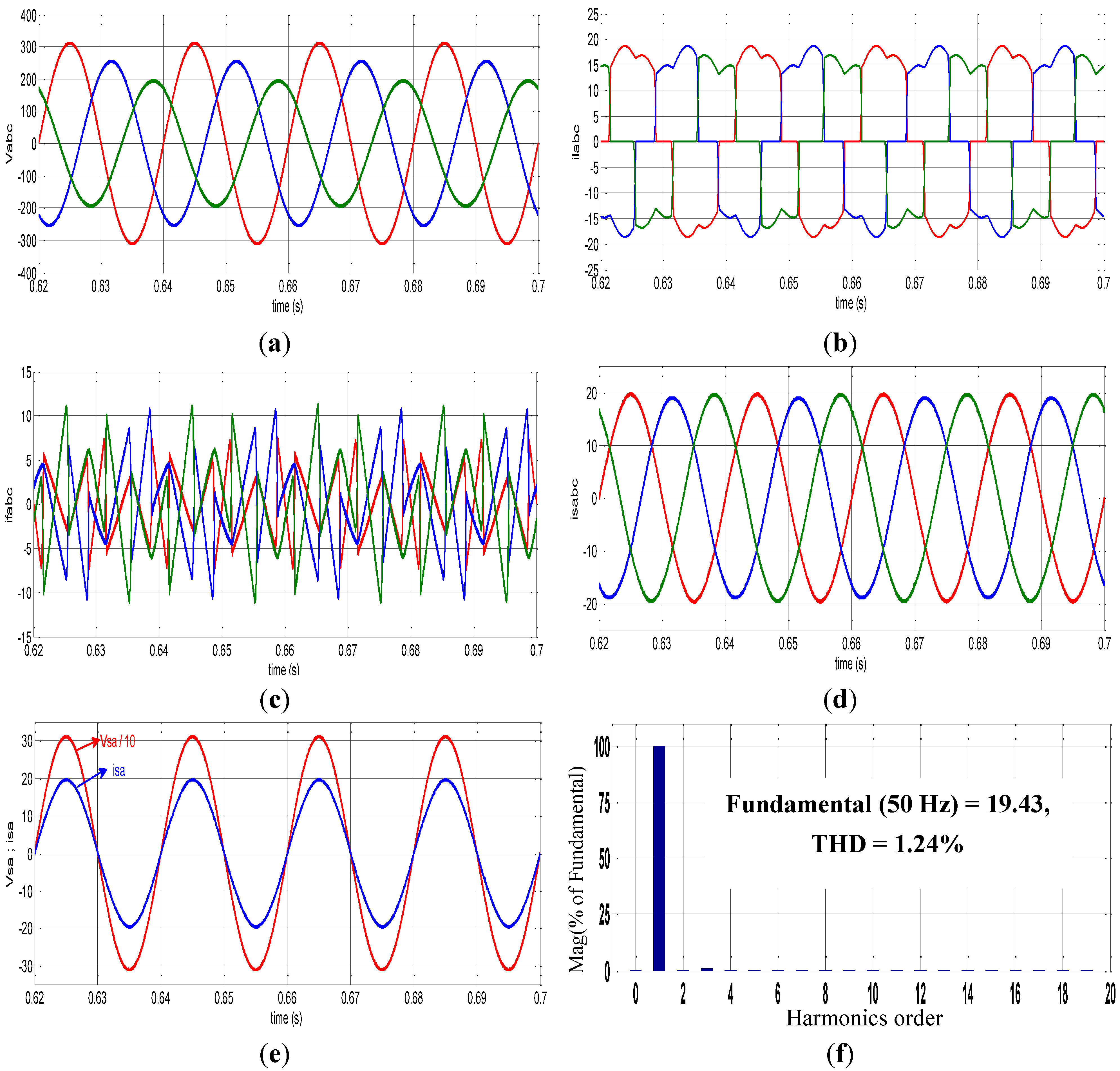
4.2.2. Case B: Unbalanced Sinusoidal Grid Voltage
The phase-b is unbalanced by 20% relatively to phase-a (vb = 180 V), while the phase-c is unbalanced by 40% relatively to phase-a (Vc = 140 V) with TUv = 22.2%. Based on results of
Figure 13, we observe that unlike standard DPC, the proposed ZDPC shows its good performance for balancing and improving the line currents (TUis = 1.27% and THDis = 1.24%).
Table 3 summarizes the comparison between standard DPC and ZDPC.
Figure 13.
Simulation results for unbalanced sinusoidal grid voltage: (a) three-phase line voltages; (b) three-phase load currents; (c) three-phase filter currents; (d) three-phase line currents; (e) line voltage and current, phase-a; (f) frequency spectrum of line current, phase-a.
Figure 13.
Simulation results for unbalanced sinusoidal grid voltage: (a) three-phase line voltages; (b) three-phase load currents; (c) three-phase filter currents; (d) three-phase line currents; (e) line voltage and current, phase-a; (f) frequency spectrum of line current, phase-a.
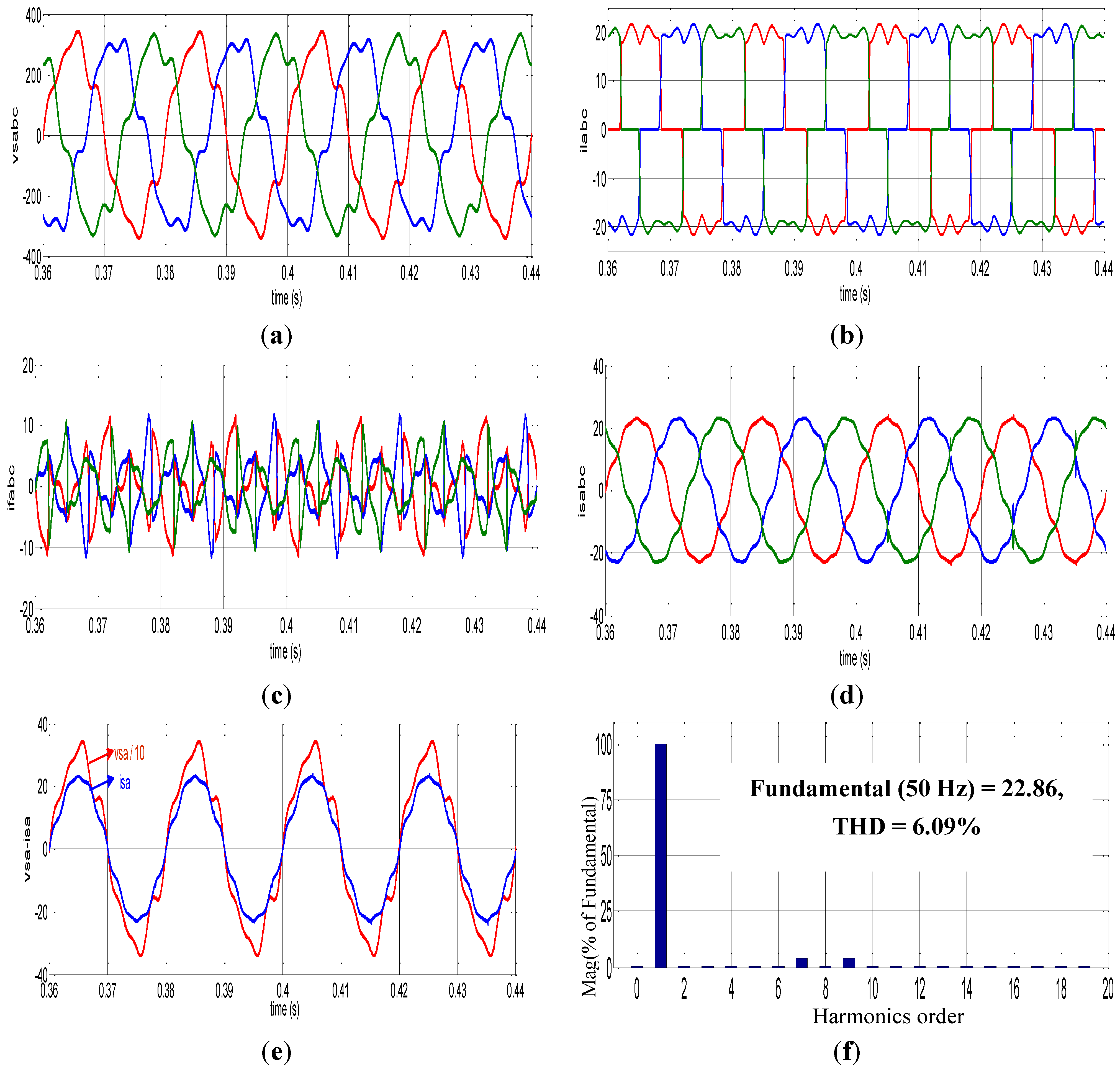
4.2.3. Case C: Balanced Distorted Grid Voltage
In this case the grid voltage is balanced but distorted with a THDv = 12.83% as shown in
Table 2. The simulation results in
Figure 14, prove the good performance of ZDPC (THDis = 0.72%) comparatively to standard DPC.
Table 3 summarizes the main results comparison.
Figure 14.
Simulation results for balanced distorted grid voltage: (a) three-phase line voltages; (b) three-phase load currents; (c) three-phase filter currents; (d) three-phase line currents; (e) line voltage and current, phase-a; (f) frequency spectrum of line current, phase-a.
Figure 14.
Simulation results for balanced distorted grid voltage: (a) three-phase line voltages; (b) three-phase load currents; (c) three-phase filter currents; (d) three-phase line currents; (e) line voltage and current, phase-a; (f) frequency spectrum of line current, phase-a.
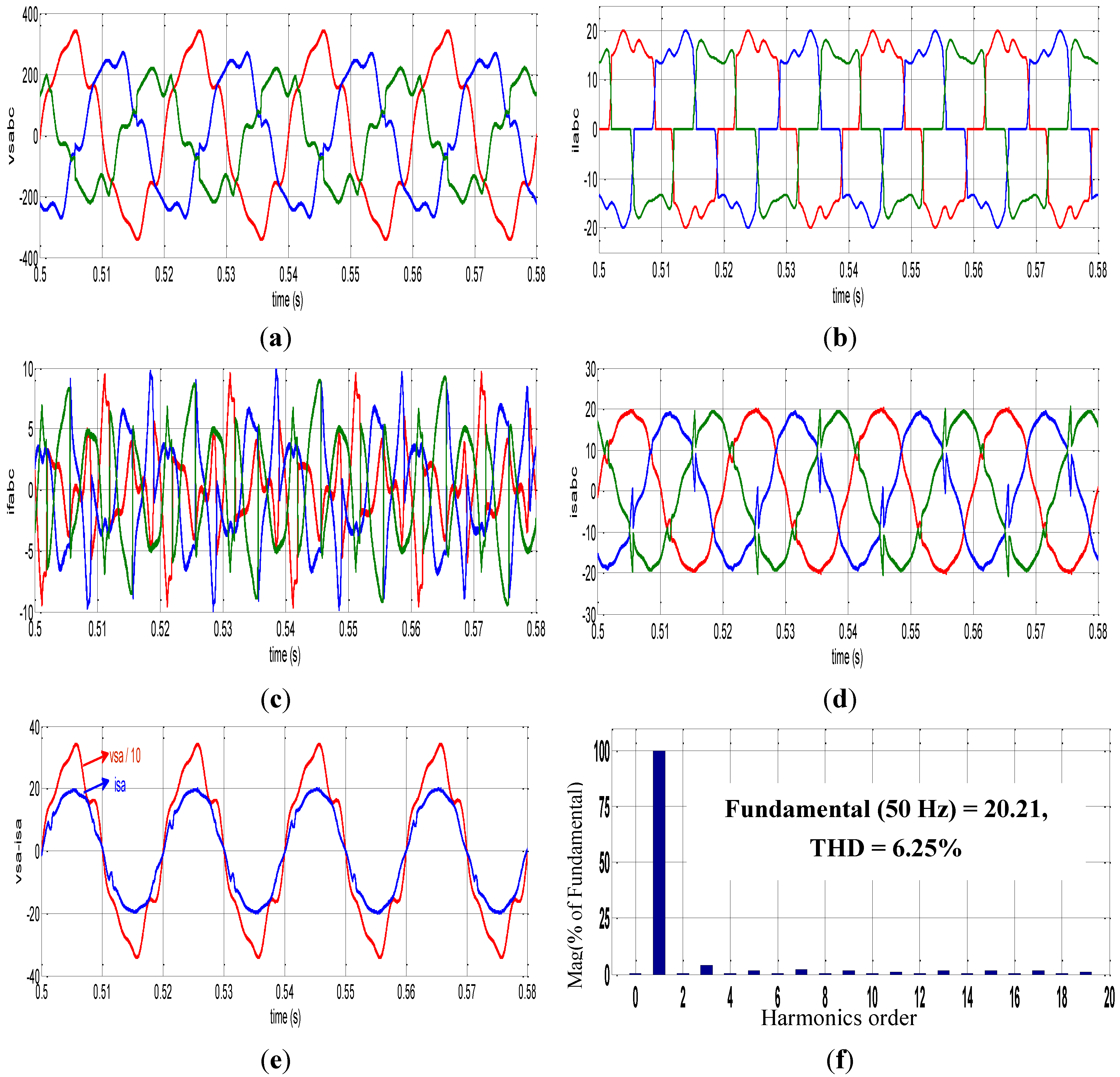
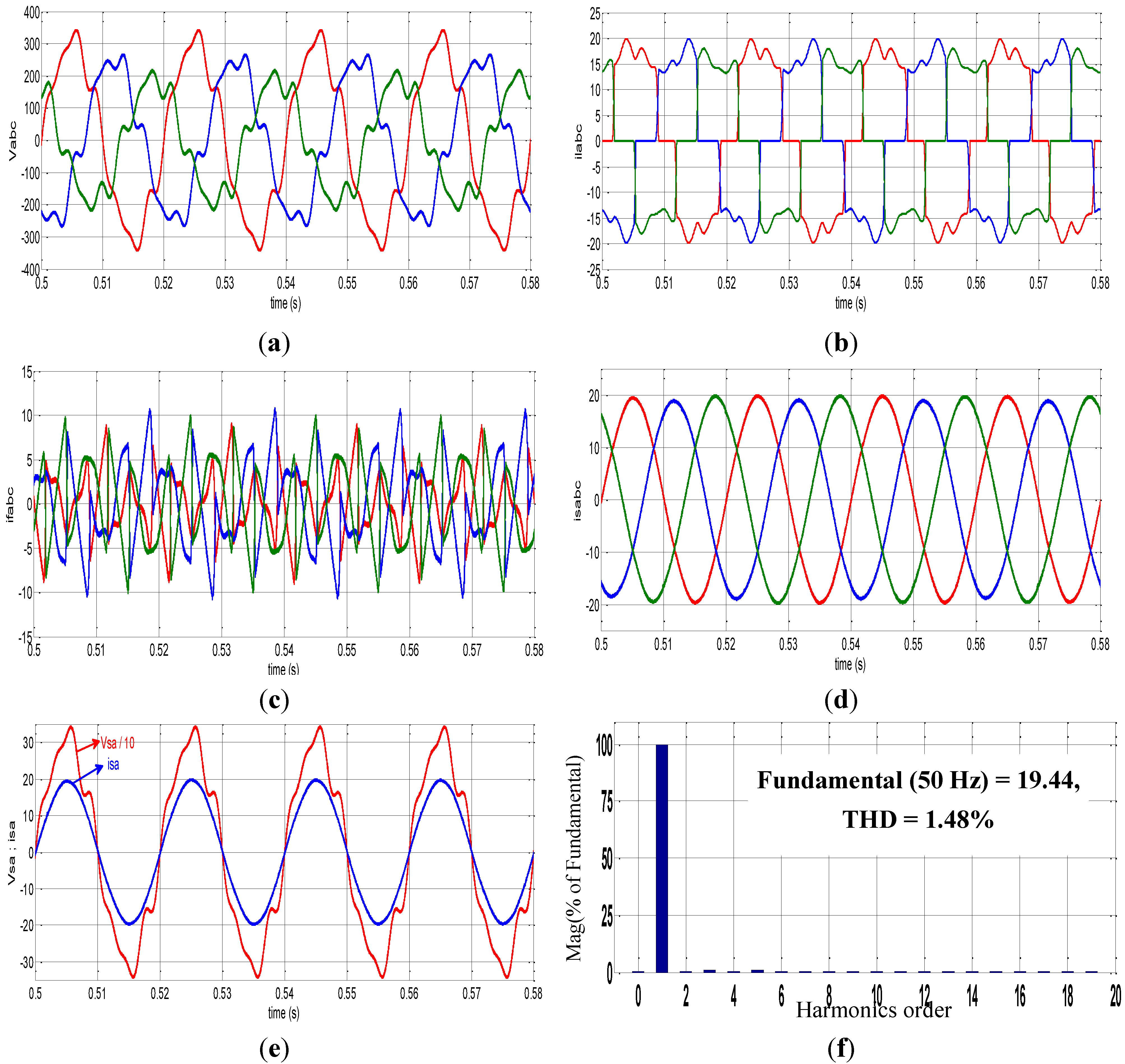
4.2.4. Case D: Unbalanced and Distorted Grid Voltage
This is the worst case. It corresponds together to unbalanced and distorted voltage as shown in
Figure 15 and
Table 2. The simulation results are shown in
Figure 15 confirm the robustness of ZDPC. Comparatively to standard DPC we can observe that the grid current is quasi sinusoidal (THDis = 1.48%), balanced (TUis = 1.41%) and synchronized with the grid voltage.
Table 3 summarizes the comparison results.
Figure 15.
simulation results of unbalanced distorted grid voltage: (a) three-phase line voltages; (b) three-phase load currents; (c) three-phase filter currents; (d) three-phase line currents; (e) line voltage and current, phase-a; (f) frequency spectrum of line current, phase-a.
Figure 15.
simulation results of unbalanced distorted grid voltage: (a) three-phase line voltages; (b) three-phase load currents; (c) three-phase filter currents; (d) three-phase line currents; (e) line voltage and current, phase-a; (f) frequency spectrum of line current, phase-a.
4.3. Comparison of ZDPC and HSF-DPC 10
In this section we compare the ZDPC to HSF-DPC published recently in [
10], with the same grid voltage conditions,
Table 4, and parameters in
Appendix.
Table 5 shows the simulation results obtained by both the proposed ZDPC and HSF-DPC given in [
10] for three cases (A, B, C). We observe that the proposed ZDPC leads to better results whatever the conditions, unlike HSF-DPC of [
10] only suitable for the case of unbalanced and distorted grid voltage and in addition in [
10] there are no experimental validation.
Table 4.
Grid voltage, load current and THD under various grid voltage conditions [
10].
Table 4.
Grid voltage, load current and THD under various grid voltage conditions [10].
| Case | Source voltage | Load current |
|---|
| vsa | vsb | vsc | iLa | iLb | iLc |
|---|
| rms (v) | THD (%) | rms (v) | THD (%) | rms (v) | THD (%) | rms (A) | THD (%) | rms (A) | THD (%) | rms (A) | THD (%) |
|---|
| A | 220 | 0 | 220 | 0 | 220 | 0 | 16.03 | 27.86 | 16.02 | 27.82 | 16.02 | 27.83 |
| B | 176 | 0 | 220 | 0 | 220 | 0 | 14.01 | 31.69 | 15.47 | 25.95 | 15.46 | 26.15 |
| C | 222.2 | 14.29 | 222.2 | 14.29 | 222.2 | 14.29 | 15.82 | 29.07 | 15.76 | 29.55 | 15.79 | 29.12 |
Table 5.
Simulation results for HSF-DPC and ZDPC strategies under three cases (A, B, C).
Table 5.
Simulation results for HSF-DPC and ZDPC strategies under three cases (A, B, C).
| Case | Control strategies | Source currents | Filter currents |
|---|
| isa | isb | isc | ifa | ifc | ifb |
|---|
| rms (A) | THD (%) | rms (A) | THD (%) | rms (A) | THD (%) | rms (A) | rms (A) | rms (A) |
|---|
| A | HSF-DPC [10] | 15.44 | 0.47 | 15.35 | 0.45 | 15.38 | 0.43 | 4.56 | 4.57 | 4.56 |
| ZDPC | 16.21 | 0.64 | 16.21 | 0.68 | 16.21 | 0.65 | 4.65 | 4.65 | 4.65 |
| B | HSF-DPC [10] | 14.38 | 1.54 | 14.53 | 2.06 | 14.33 | 2.61 | 4.64 | 4.02 | 4.46 |
| ZDPC | 15.13 | 0.8 | 15.23 | 1.10 | 15 | 0.93 | 5.03 | 3.99 | 4.47 |
| C | HSF-DPC [10] | 15 | 4.63 | 15.01 | 4.46 | 15.02 | 4.08 | 5.64 | 5.63 | 5.63 |
| ZDPC | 15.79 | 2.57 | 15.78 | 2.59 | 15.79 | 2.51 | 5.10 | 5.10 | 5.11 |
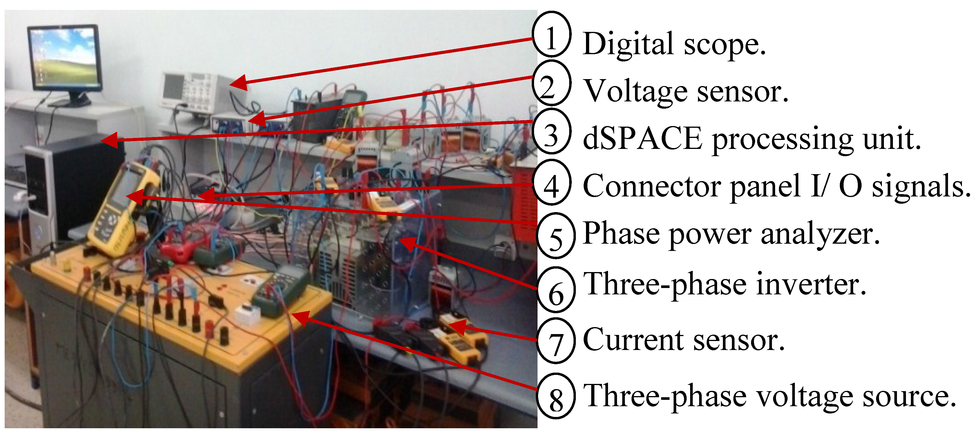
5. Experimental Results
To validate experimentally the proposed ZDPC, the experimental set up shown in
Figure 16 has been used. The control technique is implemented in dSPACE DS1104 environment, with the parameters given in
Appendix. Two different conditions are considered:
- -
Case A, the grid voltage is balanced.
- -
Case B, the grid voltage is unbalanced.
Figure 16.
Experimental set up.
Figure 16.
Experimental set up.
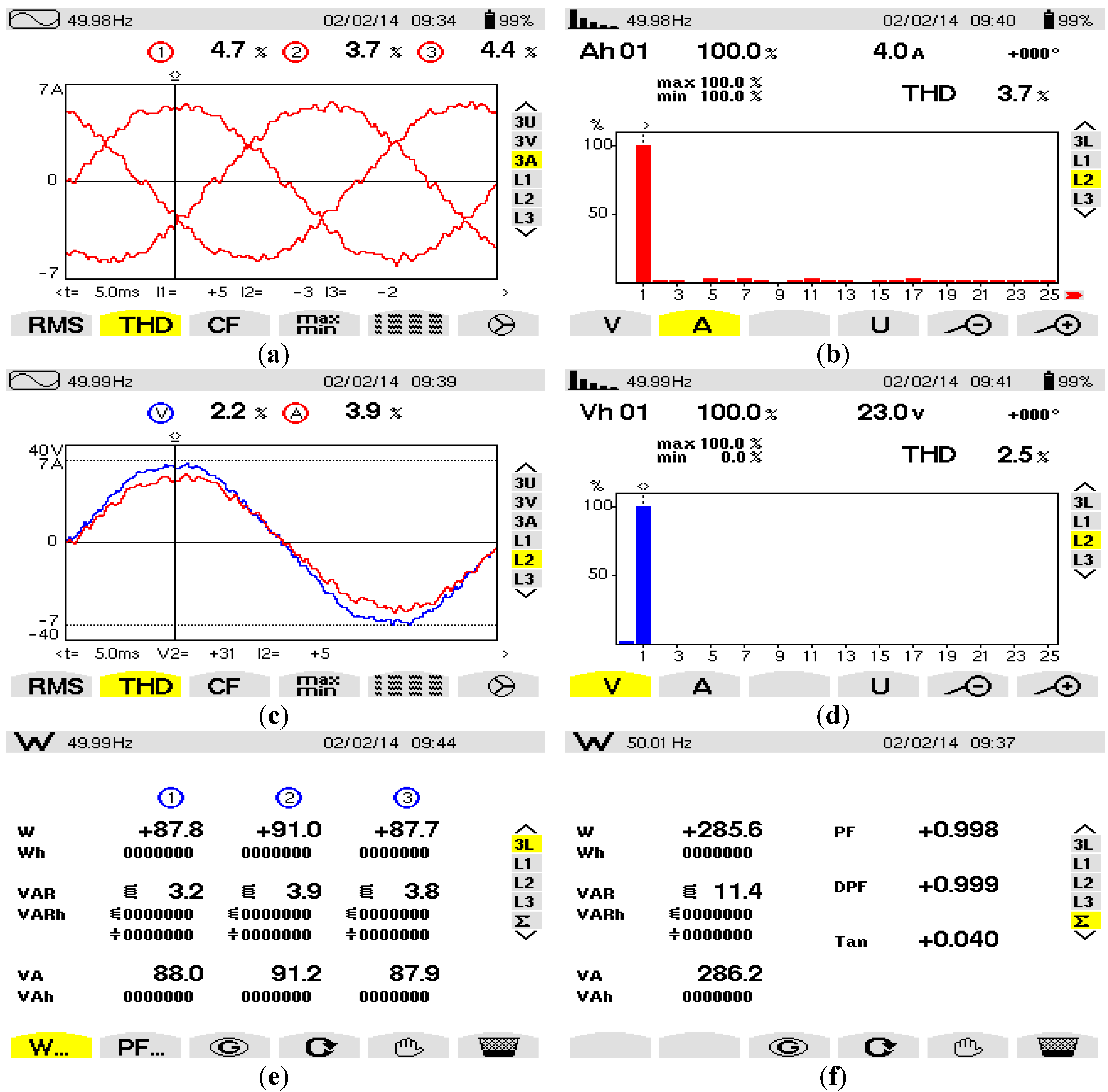
5.1. Case A: Balanced Sinusoidal Grid Voltage
The grid voltage is balanced (vs = 23 V rms).
Figure 17a,b shows a good compensation of the line current (THDisa = 4.7%, THDisb = 3.7%, THDisc = 4.4%), which is less than the IEEE-519 standard, and with a power factor close to unity.
Figure 17.
Experimental results for balanced sinusoidal grid voltage: (a) three-phase line currents with their THD; (b) frequency spectrum of line current, phase-b; (c) line voltage and current, phase-b; (d) frequency spectrum of line voltage, phase-b; (e) power balance after filtering; (f) characteristic and power balance sheet of the grid after filtering.
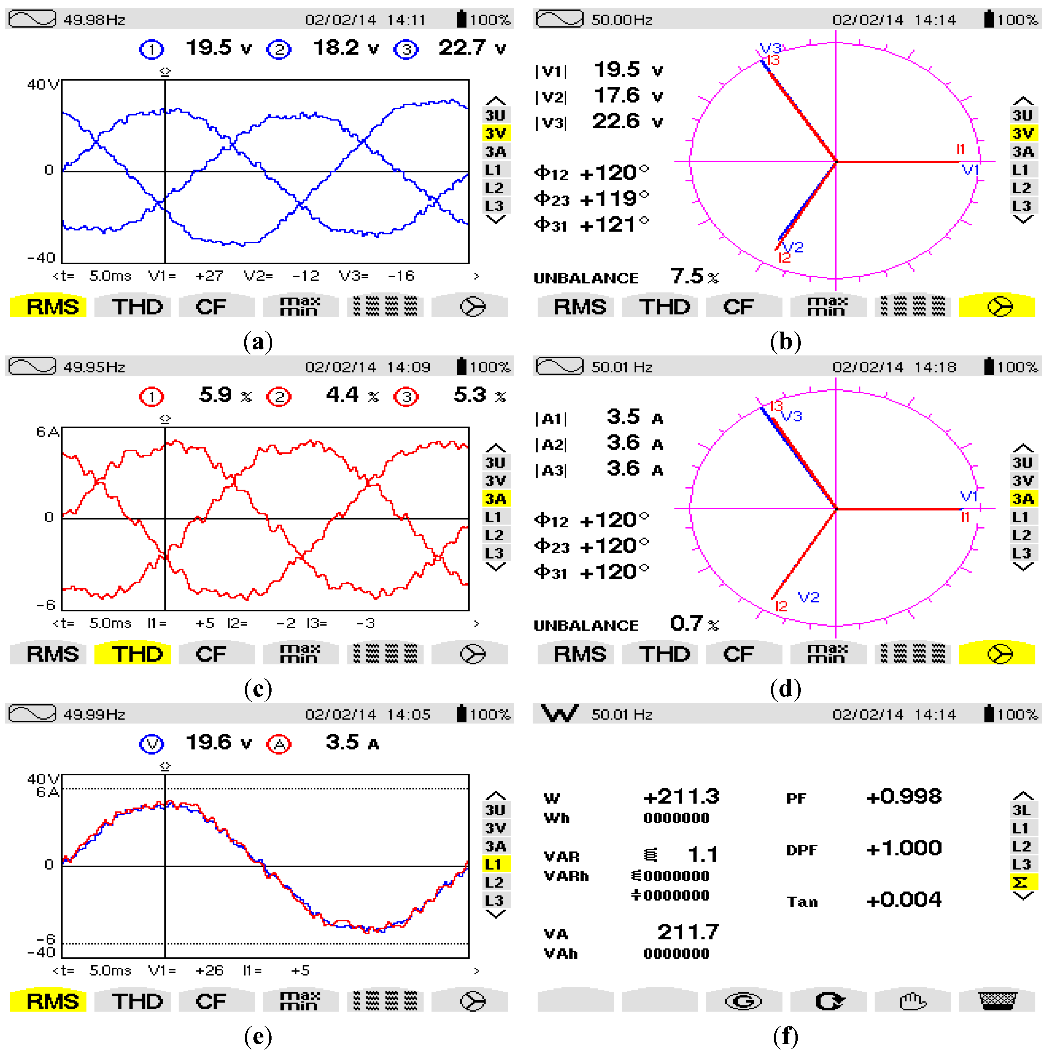
5.2. Case B: Unbalanced Sinusoidal Grid Voltage
The grid voltage is unbalanced for two phases (a and b) relatively to phase-c (V
sa = 19.5 V, V
sb = 17.6 V, V
sc = 22.6 V), with TU
v = 7.5%).
Figure 18b,c shows a good compensation of the line current (THDi
sa = 5.9%, THDi
sb = 4.4%, THDi
sc = 5.3%), and a balance (TUi
s = 0.7%), synchronized with grid voltages (
Figure 18d,e). Balance of the line current is well observed in the vector diagram (equal 0.7%),
Figure 18d. This can be further improved with the availability of the appropriate experimental parameters.
Figure 18.
Experimental results of unbalanced sinusoidal grid voltage: (a) three-phase line voltage with THD; (b) Vector diagram of line voltage and current; (c) three-phase line currents with THD after filtering; (d) Vector diagram of line voltage and current; (e) line voltage and current, phase-a; (f) characteristic and power balance sheet of the grid after filtering.
6. Conclusions
In this paper a new DPC technique called ZDPC, suitable for harmonic and reactive power compensation, has been proposed. Its effectiveness whatever the grid voltage conditions (unbalanced, distorted) has been proved, unlike the standard DPC which gives satisfying results only for balanced and undistorted grid. A HSF filter, easy to implement and effective for harmonics extraction, has been used. We changed the conventional PLL by an improved PLL based on HSF for identifying Harmonics. So the ZDPC always provides balanced grid currents with a THD lower than the standard IEEE-519. Simulation and experimental results show the good performance of the proposed approach compared to standard DPC.
Author Contributions
Kamel Djazia built the simulation model and experimental setup. Fateh Krim proposed the idea of DPC under unbalanced and distorted conditions, checked the language and responded to the reviewers. Abdelmadjid Chaoui was in charge of the experimental work. Mustapha Sarra contributed in the simulation data processing.
Nomenclature
| P | Active power |
| S | Apparent power |
| Q | Reactive power |
| D | Distortion power |
| THD | Total harmonic distortion |
| vs(a,b,c) | Voltage at the coupling point of phase (a,b,c) |
| is(a,b,c) | VSource current of phase (a,b,c) |
| If(a,b,c) | filter current of phase (a,b,c) |
| Il(a,b,c) | load current of phase (a,b,c) |
| pref | Instantaneous active power reference |
| ps | Instantaneous active power source |
| qs | Instantaneous reactive power source |
| qref | Instantaneous reactive power reference |
| θn | Sector angle |
| ih | Harmonic current |
| α,β | Component in α-β coordinates system |
| RL | Resistor of load impedance |
| LL | Inductance of load impedance |
| Rs | Resistor of source impedance |
| LS | Inductance of source impedance |
| Rf | SAPF resistor |
| Lf | SAPF inductance |
| TS | Sampling Time |
| h | Hysteresis band |
| dps,dqs | Output hysteresis controller |
| ΔPs,ΔQs | variation of active and reactive power |
Appendix
| System Parameters | Simulation [10] | Experimental |
|---|
| Source voltage | 220V (rms value) | 23V (rms value) |
| Source impedance | Rs = 0.25 mΩ, Ls = 19.4 μH | Rs = 0.1 Ω, Ls = 100 μH |
| Source frequency | 50 Hz | 50 Hz |
| Load ac impedance | RL = 1.2 mΩ, LL = 0.3 mH | RL = 0.8 Ω, LL = 2 mH |
| SAPF dc reference voltage and capacitor | Vdc = 800 V, C = 8.8 mF | Vdc = 100 V, C = 1.1 mF |
| SAPF resistor and inductance | Rf = 5 mΩ, Lf = 3 mH | Rf = 0.05 Ω, Lf = 10 mH |
| Non-linear load parameters | R = 26 Ω, L = 10 mH | R = 7 Ω, L = 2 mH |
| Sampling Time | Ts = 1 µs | Ts = 50 µs |
Conflicts of Interest
The authors declare no conflict of interest.
References
- Zaveri, T.; Bhalja, B.; Zaveri, N. Comparison of control strategies for DSTATCOM in three-phase, four-wire distribution system for power quality improvement under various source voltage and load conditions. Electr. Power Energy Syst. 2012, 43, 582–594. [Google Scholar]
- Elbar, M.; Mahmoudi, M.O.; Aliouane, K.; Merzouk, I.; Naas, B. Etude Comparative de la Méthode pqo et la Méthode pqr en vue de la Compensation des Harmoniques dans les Réseaux à Quatre Fils. In Proceedings of the 3rd International Conference on Electrical Engineering, Algiers, Algeria, 19–21 May 2009. (In French)
- Hamadi, A. Contribution à L’étude des Filtres Hybrides de Puissance Utilises Pour Améliorer la Qualité de L’énergie dans le Réseau Electrique de Distribution. Ph.D. Dissertation, University of Quebec, Montréal, QC, Canada, 14 September 2010. [Google Scholar]
- Akagi, H. Active harmonic filters. Proc. IEEE 2005, 93, 2128–2141. [Google Scholar] [CrossRef]
- Xu, F.; Tolbert, L.M.; Xu, Y. Critical evaluation of FBD, PQ and generalized non-active power theories. In Proceedings of the European Conference on Power Electronics and Applications (IEEE ECCE Europe), Birmingham, UK, 30 August–1 September 2011.
- Djazia, K.; Krim, F.; Sarra, M. Active filter under unbalanced and distorted conditions. In Proceedings of the 2013 IEEE 7th International Power Engineering and Optimization Conference (PEOCO2013), Langkawi, Malaysia, 3–4 June 2013; pp. 661–666.
- Takahashi, T.; Noguchi, T. A new quick-response and high-efficiency control strategy of induction motor. IEEE Trans. Ind. Appl. 1986, 22, 820–827. [Google Scholar] [CrossRef]
- Noguchi, T.; Tomiki, H.; Kondo, S.; Takahashi, I. Direct power control of PWM converter without power-source voltage sensors. IEEE Trans. Ind. Appl. 1998, 34, 473–479. [Google Scholar] [CrossRef]
- Bouafia, A. Techniques de commande prédictive et floue pour les systèmes d’électronique de puissance: Application aux redresseurs a MLI. Ph.D. Dissertation, University of Sétif, Sétif, Algeria, 6 June 2010. [Google Scholar]
- Mesbahi, N.; Ouari, A.; Ould Abdeslam, D. Direct power control of shunt active filter using high selectivity filter (HSF) under distorted or unbalanced conditions. Electr. Power Syst. Res. 2014, 108, 113–123. [Google Scholar] [CrossRef]
- Bouafia, A.; Gaubert, J.-P.; Chaoui, A. Direct power control scheme based on disturbance rejection principle for three-phase PWM AC/DC converter under different input voltage conditions. J. Electr. Syst. 2012, 8, 367–383. [Google Scholar]
- Bouafia, A.; Gaubert, J.-P.; Chaoui, A. High performance direct power control of three-phase PWM boost rectifier under different supply voltage conditions. In Proceedings of the European Conference on Power Electronics and Applications, EPE, Lille, France, 3–5 September 2013.
- Chaoui, A. Filtrage Actif Triphase Pour Charges non Linéaires. Ph.D. Dissertation, University of Sétif, Sétif, Algeria, 5 October 2010. [Google Scholar]
- Chaoui, A.; Gaubert, J.P.; Krim, F. Power quality improvement using DPC controlled three-phase shunt active filter. Electr. Power Syst. Res. 2010, 80, 657–666. [Google Scholar]
- Alali, M. Contribution à l’Etude des Compensateurs Actifs des Réseaux Electriques Basse Tension. Ph.D. Dissertation, Louis Pasteur University, Strasbourg I, France, 12 September 2002. [Google Scholar]
- Long, B.; Ryu, J.H.; Chong, K.T. Optimal switching table-based sliding mode control of an energy recovery Li-Ion power accumulator battery pack testing system. Energies 2013, 6, 5200–5218. [Google Scholar] [CrossRef]
- Benhabib, M.C.; Saadate, S. A new robust experimentally validated phase locked loop for power electronic control. EPE J. 2005, 15, 36–46. [Google Scholar]
- Karimi, S. Continuité de Service des Convertisseurs Triphasés de Puissance et Prototypage “FPGA in the Loopˮ: Application au Filtre Actif Parallèle. Ph.D. Dissertation, Henri Poincaré University Nancy-I, Nancy, France, 26 January 2009. [Google Scholar]
© 2015 by the authors; licensee MDPI, Basel, Switzerland. This article is an open access article distributed under the terms and conditions of the Creative Commons Attribution license (http://creativecommons.org/licenses/by/4.0/).


