Abstract
The main objective of this paper was to study a bidirectional direct current to direct current converter (BDC) topology with a high voltage conversion ratio for electric vehicle (EV) batteries connected to a dc-microgrid system. In this study, an unregulated level converter (ULC) cascaded with a two-phase interleaved buck-boost charge-pump converter (IBCPC) is introduced to achieve a high conversion ratio with a simpler control circuit. In discharge state, the topology acts as a two-stage voltage-doubler boost converter to achieve high step-up conversion ratio (48 V to 385 V). In charge state, the converter acts as two cascaded voltage-divider buck converters to achieve high voltage step-down conversion ratio (385 V to 48 V). The features, operation principles, steady-state analysis, simulation and experimental results are made to verify the performance of the studied novel BDC. Finally, a 500 W rating prototype system is constructed for verifying the validity of the operation principle. Experimental results show that highest efficiencies of 96% and 95% can be achieved, respectively, in charge and discharge states.
1. Introduction
In recent years, to reduce fossil energy consumption, the development of environmentally friendly dc-microgrid technologies have gradually received attention [1,2,3,4,5,6,7]. As shown in Figure 1, a typical dc-microgrid structure includes a lot of power electronics interfaces such as bidirectional grid-connected converters (GCCs), PV/wind distributed generations (DGs), battery energy systems (BES), electric vehicles (EVs), and so on [4]. They connect together with a high-voltage dc-bus, so that dc home appliances can draw power directly from the dc-bus. In this system, the main function of GCCs is to maintain the dc-bus voltage constant, while in order to ensure the reliability of operation for dc-microgrids, a mass of BES can usually be accessed into the system. Electric vehicles (EVs) can also provide auxiliary power services for dc-microgrids, which makes clean and efficient battery-powered conveyance possible by allowing EVs to power and be powered by the electric utility. Usually, in dc-microgrid systems, when the voltage difference between the EV battery, BES and the dc-bus is large, a bidirectional dc/dc converter (BDC) with a high voltage conversion ratio for both buck and boost operations is required [4,7]. In the previous literatures, BDCs circuit topologies of the isolated [8,9,10] and non-isolated type [11,12,13,14,15,16,17,18,19,20,21,22,23] have been described for a variety of system applications. Isolated BDCs use the transformer to implement the galvanic isolation and to comply with the different standards. Personnel safety, noise reduction and correct operation of protection systems are the main reasons behind galvanic isolation. In contrast with isolated BDCs, non-isolated BDCs lack the galvanic isolation between two sides, however, they offer the benefits of smaller volume, high reliability, etc., so they have been widely used for hybrid power system [24,25].
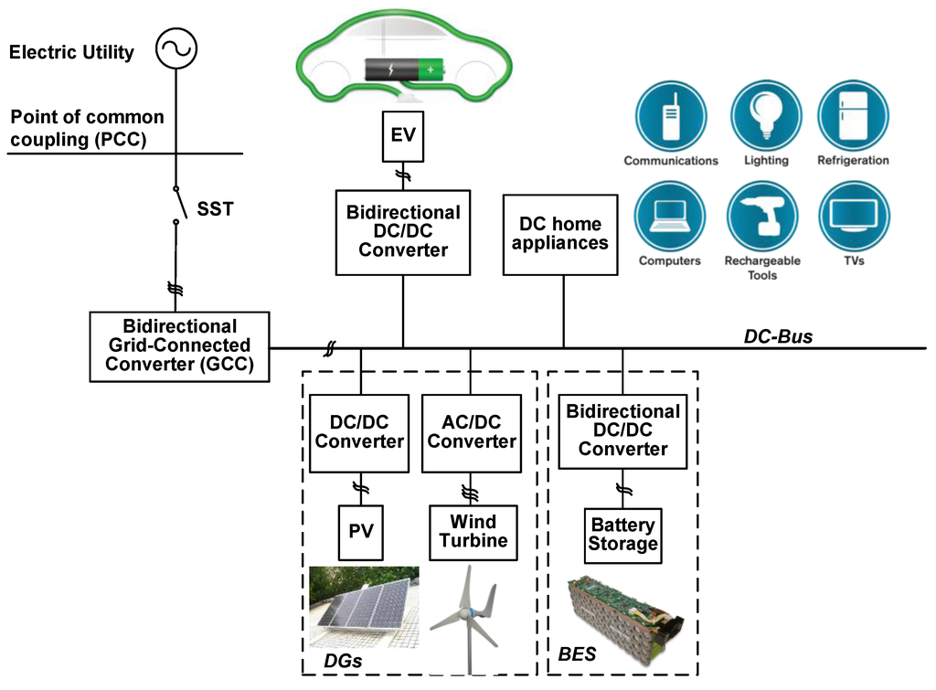
Figure 1.
A typical dc-microgrid structure [4].
Compared with isolated types, BDCs with coupled-inductors for non-isolated applications possess simpler winding structures and lower conduction losses [12,13,14,15,16,17]. Furthermore, the coupled-inductor techniques can achieve easily the high voltage conversion ratio by adjusting the turn ratio of the coupled-inductor. However, the energy stored in the leakage inductor of the coupled inductor causes a high voltage spike in the power devices. Wai et al. [12,13] investigated a high-efficiency BDC, which utilizes only three switches to achieve the objective of bidirectional power flow. Also, the voltage-clamped technique was adopted to recycle the leakage energy so that the low-voltage stress on power switches can be ensured. To reduce the switching losses, Hsieh et al. proposed a high efficiency BDC with coupled inductor and active-clamping circuit [16]. In this reference, a low-power prototype was built to verify the feasibly.
As shown in Figure 2, Liang et al. [17] proposed a bidirectional double-boost cascaded topology for a renewable energy hybrid supply system, in which the energy is transferred from one stage to another stage to obtain a high voltage gain. Hence their conduction losses are high and it requires a large number of components.
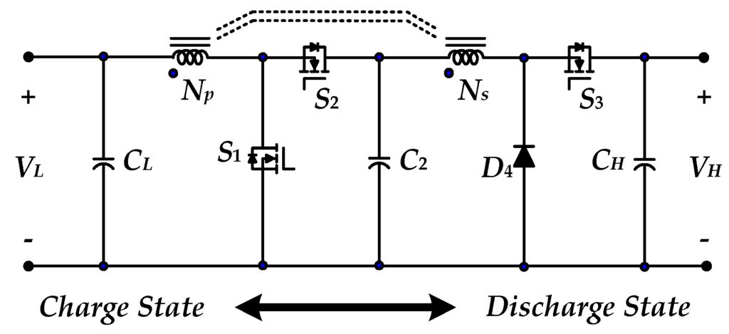
Figure 2.
Circuit structure of the bidirectional double-boost cascaded topology [17].
Chen et al. [18] proposed a reflex-based BDC to achieve the energy recovery function for batteries connected to a low-voltage micro dc-bus system. In [18], a traditional buck-boost BDC was adopted, however, the voltage conversion ratio is limited because of the equivalent series resistance (ESR) of the inductors and capacitors and effect of the active switches [19].
To increase the voltage gain of the converter, the capacitors are switched and it will act as a charge-pump. The main advantage of the switched capacitor-based boost converter is that there is no need of a transformer or inductors. The main drawbacks of this topology are the complexity of the topology, high cost, low power level and high pulsating current in the input side [11,21]. In order to increase the conversion efficiency and voltage conversion ratio, multilevel combined the switched-capacitor techniques have been proposed to achieve lower stress on power devices [20,21,22,23]. As shown in Figure 3, in [22,23] two converters regulated the reasonable voltage conversion ratio with a simple pulse-width_modulation (PWM) control. However, if a high voltage conversion ratio must be provided, more power switches and capacitors are indeed required. Furthermore, although the extreme duty cycle can be avoided, the input current ripple is large due to their single-phase operation which renders these BDCs unsuitable for high current and low ripple applications.
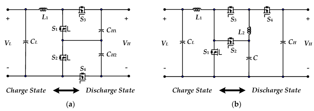
Figure 3.
Two multilevel combined the switched-capacitor topologies: (a) circuit structure in [22]; (b) circuit structure in [23].
The objective of this paper is to study and develop a novel BDC for applications involving EVs connected to dc-microgrids. To meet the high current, low current ripple, and high voltage conversion ratio demands, the studied topology consists of an unregulated level converter (ULC) cascaded with a two-phase interleaved buck-boost charge-pump converter (IBCPC). In discharge state, the topology acts as a two-stage cascaded two-phase boosting converter to achieve a high step-up ratio. In charge state, the topology acts as two-stage cascaded two-phase bucking converter to achieve a high step-down ratio. The extreme duty cycle of power devices will not occur for bidirectional power flow conditions, thus not only can the output voltage regulation range be further extended but also the conduction losses can be reduced. In addition, the two-stage structure benefits reducing the voltage stress of active switches, which enables one to adopt the low-voltage rating and high performance devices, thus the conversion efficiency can be improved. The remainder of this paper is organized as follows: first, the converter topology and the operation principles of the studied BDC are illustrated in Section 2. Then, steady-state characteristic analyzes are presented in Section 3. A 500 W laboratory prototype is also constructed, and the corresponding simulation results, as well as experimental results, are provided to verify the feasibility of the studied BDC in Section 4. Finally, some conclusions are offered in the last section.
2. Proposed BDC Topology and Operation Principles
The system configuration for the studied BDC topology is depicted in Figure 4. The system contains two parts, including a ULC and a two-phase IBCPC. The major symbol representations are summarized as follows: VH and VL denote the high-side voltage and low-side voltage, respectively. L1 and L2 represent two-phase inductors of IBCPC. CB denotes the charge-pump capacitor. CH and CL are the high-side and low-side capacitors, respectively. The symbols, Q1~Q4, and S1~S4, respectively, are the power switches of the IBCPC and ULC.
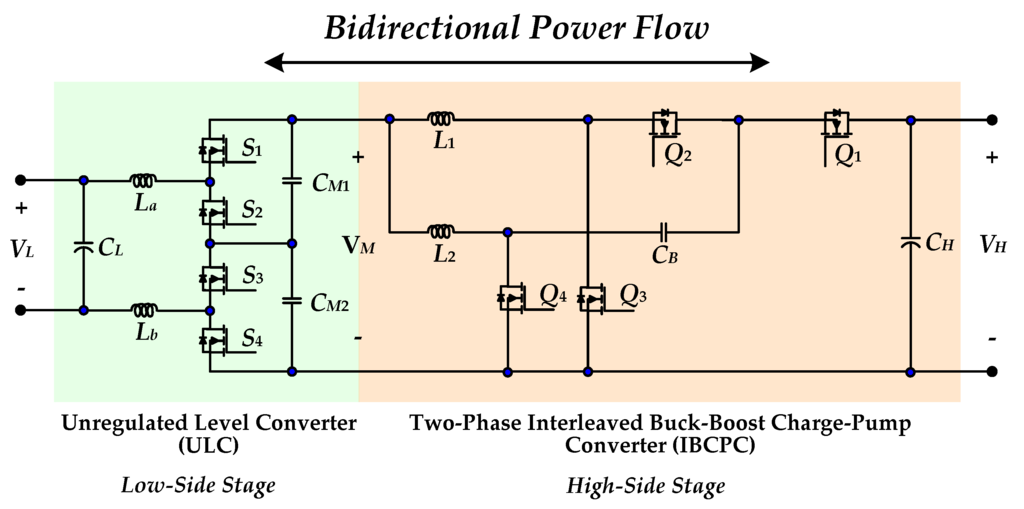
Figure 4.
System configuration of the novel BDC topology.
In this study, as the low-side stage, a high efficiency magnetic-less ULC with bidirectional power flow is adopted to output a fixed voltage for a given input voltage. Because only a small sized high frequency line filter (La, Lb) is required, it can substantially boost the power density of the low-side stage. Furthermore, by leaving the voltage regulation to another high-side stage, the studied BDC for the low-side stage with fixed 2:1 under charge state operation or 1:2 conversion ratio under discharge state operation, can achieve high efficiency with a relatively low-side voltage in whole load range. As to the high-side stage, the structure of two-phase IBCPC is similar to a conventional buck-boost converter except two active switches in series and a charge-pump capacitor (CB) employed in the power path. The circuit structure is simple and it can reach the high voltage conversion ratio with a reasonable duty cycle. Therefore, it can reduce the conduction loss of the switch, to further upgrade the efficiency of the whole bidirectional converter.
The studied BDC topology can deliver energy in both directions. When the energy flows from VH to VL, it operates in charge state (i.e., buck operation); Q1 and Q2 are controlled to regulate the output. Thus, Q1 and Q2 are defined as the active switches, while Q3 and Q4 are the passive switches. The passive switches work as synchronous rectification (SR). When the energy flows from VL to VH, it operates in discharge state (i.e., boost operation); Q3 and Q4 are controlled to regulate the output. Thus, Q3 and Q4 are defined as the active switches, while Q1 and Q2 are the passive switches.
In this study, the following assumptions are made to simplify the converter analyzes as follows: (1) the converter is operated in continuous conduction mode (CCM); (2) capacitors CH and CL is large enough to be considered as a voltage source; (3) the middle-link voltage VM = VM1 + VM2 is treated as a pure dc and considered as constant; (4) the two inductor L1 and L2 have the same inductor Ls; (5) all power semiconductors are ideal; (6) the charge-pump voltage VCB is treated as a pure dc and considered as constant.
2.1. Charge State Operation
Figure 5 and Figure 6 show the circuit configuration and characteristic waveforms of the studied BDC in charge state, respectively. It can be seen that switches Q1 and Q2 are driven with the phase shift angle of 180°; Q3 and Q4 work as synchronous rectification. In charge state, when S1, S3 are turned on and S2, S4 are turned off; or else S2, S4 are turned on and S1, S3 are turned off. The low-side voltage VL is half the middle-link voltage VM, i.e., VL = 0.5VM. In this state, one can see that, when duty ratio of Q1 and Q2 are smaller than 50%, there are four operating modes according to the on/off status of the active switches.
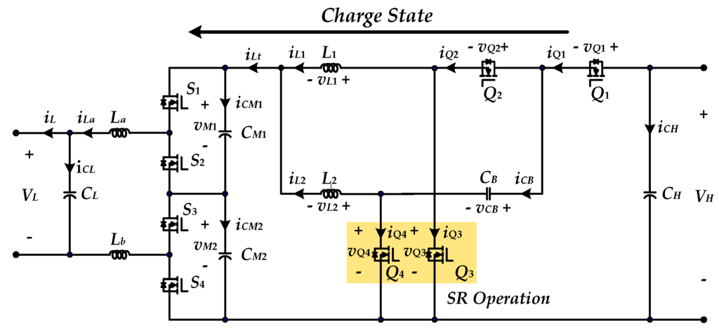
Figure 5.
Circuit configuration of the studied BDC in charge state.

Figure 6.
Characteristic waveforms of the studied BDC in charge state.
Referring to the equivalent circuits shown in Figure 7, the operating principle of the studied BDC can be explained briefly as follows.

Figure 7.
Equivalent circuits of the modes during different intervals in charge state: (a) Mode 1; (b) Mode 2, Mode 4; (c) Mode 3.
2.1.1. Mode 1 [t0 < t ≤ t1]
The interval time is DdTsw, in this mode, switches Q1, Q3 turned on and switches Q2, Q4 are all off. The voltage across L1 is the negative middle-link voltage, and hence iL1 decreases linearly from the initial value. Also, the voltage across L2 is the difference of the high-side voltage VH, the charge-pump voltage VCB, and the middle-link voltage VM, and its level is positive. The voltages across inductances L1 and L2 can be represented as:
2.1.2. Mode 2 [t1 < t ≤ t2]
For this operation mode, the interval time is (0.5 − Dd)Tsw, switches Q3, Q4 are turned on and switches Q1, Q2 are all off. Both voltages across inductors L1 and L2 are the negative middle-link voltage VM, hence iL1 and iL2 decrease linearly. The voltages across inductances L1 and L2 can be represented as:
2.1.3. Mode 3 [t2 < t ≤ t3]
For this operation mode, the interval time is DdTsw, switches Q2, Q4 are turned on and switches Q1 and Q3 are all off. The voltage across L1 is the difference between the charge-pump voltage VCB with the middle-link voltage VM, and L2 is keeping the negative middle-link voltage, the voltages across inductances L1 and L2 can be represented as follows:
2.1.4. Mode 4 [t3 < t ≤ t4]
From this operation mode, the interval time is (0.5 − Dd)Tsw. Switches Q3, Q4 are turned on and switches Q1, Q2 are all off, and its operation is the same with that of Mode 2.
2.2. Discharge State Operation
Figure 8 and Figure 9 show the circuit configuration and characteristic waveforms of the studied BDC in discharge state, respectively. As can be seen these figures, switches Q3, Q4 are driven with the phase shift angle of 180°; Q1, Q2 are used for the synchronous rectifier. In discharge state, when S1, S3 are turned on and S2, S4 are turned off; or else S2, S4 are turned on and S1, S3 are turned off. The low voltage VL will charge the CM1 and CM2 to make VM1 and VM2 equal to VL, the middle-link voltage VM is then twice the low-side voltage VL, i.e., VM = 2VL.
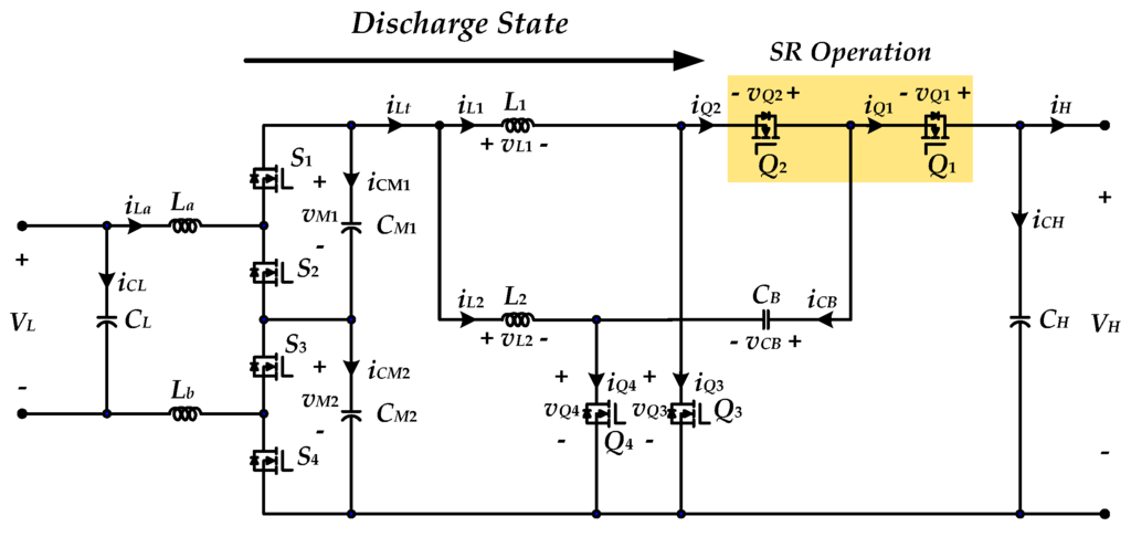
Figure 8.
Circuit configuration of the studied BDC in discharge state.

Figure 9.
Characteristic waveforms of the studied BDC in discharge state.
Referring to the equivalent circuits shown in Figure 10, the operating principle of the studied BDC can be explained briefly as follows:

Figure 10.
Equivalent circuits of the modes during different intervals in discharge state: (a) Mode 1, Mode 3; (b) Mode 2; (c) Mode 4.
2.2.1. Mode 1 [t0 < t ≤ t1]
The interval time is (Db − 0.5)Tsw, switches Q3 and Q4 are turned on; switches Q1 and Q2 are all off. For the high-side stage, the middle-link voltage VM stays between inductance L1 and L2, making the inductance current increase linearly, and begins to deposit energy. The voltages across inductances L1 and L2 can be represented as:
2.2.2. Mode 2 [t1 < t ≤ t2]
In this operation mode, the interval time is (1 − Db)Tsw. Switch Q1, Q3 remains conducting and Q2, Q4 are turned off. The voltages across inductances L1 and L2 can be represented as:
2.2.3. Mode 3 [t2 < t ≤ t3]
In this operation mode, the circuit operation is same as Mode 1.
2.2.4. Mode 4 [t3 < t ≤ t4]
In this operation mode, the interval time is (1 − Db)Tsw. For the low-side stage, switches Q1, Q3 are turned off and Q2, Q4 are turned on. The energy stored in inductor L1 is now released energy to charge-pump capacitor CB for compensating the lost charges in previous modes. The output power is supplied from the capacitor CH. The voltages across inductances L1 and L2 can be represented as:
3. Steady-State Analysis
3.1. Voltage Conversion Ratio
In charge state, VH is the input and VL is the output. According to Equations (1)–(5) and based on the voltage-second balance principle in L1 and L2, the voltage conversion ratio Md in charge state can be derived as:
In Equation (11), Dd is the duty cycle of the active switches Q1 and Q2. As can be seen, the voltage conversion ratio in charge state is one-fourth of that of the conventional buck converter. Similarly, in discharge state, VL is the input and VH is the output. According to Equations (6)–(10) and based on the voltage-second balance principle in L1 and L2, the voltage conversion ratio Mb in discharge state can be derived as:
where Db is the duty cycle of the active switches Q3 and Q4. As can be seen, the voltage conversion ratio in discharge state is four times of that of the conventional boost converter.
Figure 11 shows that the studied BDC demands a smaller duty cycle for the active switches to produce the same voltage conversion ratio, or can produce a higher voltage conversion ratio at the same duty cycle when compared with the traditional BDC [18] and the previous BDC in [22]. Furthermore, the voltage conversion ratio of studied BDC is higher than that of the BDC proposed in [23], under a reasonable range of 25%~75% duty cycles.
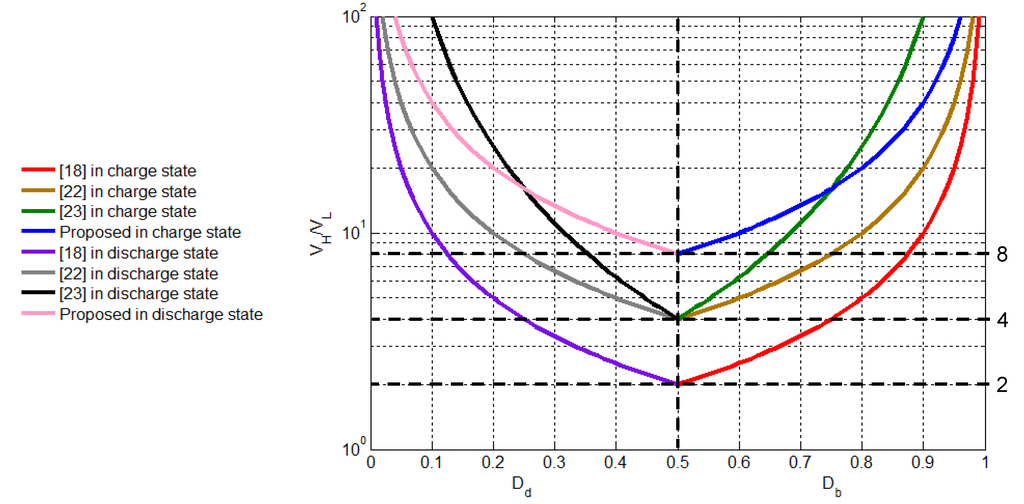
Figure 11.
Comparison of voltage conversion ratios produced by the studied BDC, the converters introduced in [18,22,23].
3.2. Voltage Stress of the Switches
Whenever the ULC works as a back or front-end stage, the open circuit voltage stress on the switches S1~S4 of ULC is equal to the low-side input voltage VL, as follows:
The particular inherent feature of the ULC benefits the low conduction losses can be achieved by adopting the low-voltage MOSFETs.
As to the high-side stage of the studied BDC, based on the aforementioned operation analyzes in Section 2, the open circuit voltage stress of switches Q1~Q4 can be obtained directly as:
3.3. Inductor Current Ripple
The studied BDC can operate not only in charge state but also in discharge state. Thus, the inductor can be calculated in either charge or discharge state. According to Equations (1)–(5), the total ripple current of the inductor of the studied BDC in charge state can be expressed as:
Similarly, in discharge state, according to Equations (6)–(10), the total ripple current of the inductor of the studied BDC in discharge state can be expressed as:
Figure 12 shows the normalized ripple current of the inductor of the studied BDC, the traditional BDC [18], and previous BDCs in [22,23], where the inductor and the switching frequency of these three BDCs are equal, respectively. The ripple current of the traditional BDC at 50% duty cycle is normalized as one.

Figure 12.
Comparison of the normalized ripple current of the inductor among the studied BDC, the converters introduced in [18,22,23].
It can be seen that from Figure 12, the maximum ripple current of the inductor of studied BDC is only one-fourth of that of a traditional BDC. On the other and, if the ripple currents are equal, the inductor of the studied BDC is only one-fourth of that of traditional BDC [18], which means that the studied BDC has a better dynamic response. From Figure 12, the ripple current of studied BDC is smaller than that of the converter in [22], under a reasonable range of 35%~65% duty cycles. Furthermore, the ripple current of the previous BDC proposed in [23] is higher than that of the one proposed in this study, under a reasonable range of 30%~70% duty cycles.
3.4. Boundary Conduction Mode
The boundary normalized inductor time constant τL,B can be defined as:
where R is low-side input equivalent resistance.
During boundary conduction mode (BCM), the input current BDC can be derived as:
Substituting Equation (19) into (18), the boundary normalized time constant in charge state can be expressed as:
Similarly, in discharge state, the input current of the studied BDC can be obtained as:
The boundary normalized time constant in discharge state can be expressed as:
Figure 13 shows the plots of boundary normalized inductor time constant curves τLd,B and τLb,B in charge and discharge states. The BDC in charge state operates in CCM when τLd is designed to be higher than the boundary curve of τLd,B. The studied BDC in discharge state operates in discontinuous conduction mode (DCM) when τLb is selected to be lower than the boundary curve of τLb,B.

Figure 13.
Normalized boundary inductances time constant in charge and discharge states.
Figure 14 shows the boundary inductances curve of the studied BDC in charge and discharge states. If the inductance is selected to be larger than the boundary inductance, the studied BDC will operate in CCM. The studied BDC can operate not only in charge state but also in discharge state, the boundary inductance can be derived as below from Equations (19) and (21), respectively.
where Pout is the output power.

Figure 14.
Boundary inductances in various power conditions.
3.5. Selection Considerations of Charge-Pump Capacitor
For the proposed BDC in charge state operation, the ripple voltage of the charge-pump capacitor CB can be obtained as follows:
where:
From Equation (25), it is known that although a capacitor with low capacitance is used for charge-pump capacitor CB, the voltage ripple can be reduced by increasing the switching frequency. The root mean square (RMS) value of the current through the charge-pump capacitor is
3.6. Summaries of Component Stress and Loss
For stress and loss analysis, it is assumed that the studied BDC operates with Dd < 0.5 and Db > 0.5 for charge and discharge modes, respectively. The results of component stress can be summarized as in Table 1. Furthermore, equations for loss analysis can be summarized as in Table 2, where Qg represents the MOSFET total gate charge; tr is rise time, it’s the period after the vGS reaches threshold voltage vGS(th) to complete the transient MOSFET gate charge; tf is fall time, it’s the time where the gate voltage reaches the threshold voltage vGS(th) after MOSFET turn-off delay time [26].

Table 1.
Stress analysis results at steady-state.

Table 2.
Loss equations at steady-state.
4. Simulation and Experimental Results
In order to illustrate the performance of the studied BDC, a laboratory prototype circuit is simulated and experimented. To avoid all elements suffer from high-current stress at DCM operation, resulting in high conduction and core losses. The studied BDC operates at CCM, and its parameters and specifications of the constructed hardware prototype are given as below:
- (1)
- high-side voltage VH: 385 V;
- (2)
- low-side voltage VL: 48 V;
- (3)
- rated power Po: 500 W;
- (4)
- switching frequency fsw: 20 kHz;
- (5)
- capacitors CH = CL = 33 μF, CM1 = CM2 = 33 μF, CB = 10 μF; (ESR of CH, RCH = 0.064 Ω; ESR of CL, RCL = 0.062 Ω, ESR of CM1, RCM1 = 0.16 Ω; ESR of CM2, RCM2 = 0.16 Ω; ESR of CB, RCB = 0.062 Ω);
- (6)
- inductors L1 = L2 = Ls = 800 μH; La = Lb = 1.5 μH (IHLP-6767GZ-A1); (ESR of L1, RL1 = 0.18 Ω, ESR of L2, RL2 = 0.18 Ω, ESR of La, RLa = 13.6 mΩ; ESR of Lb, RLb = 13.6 mΩ);
- (7)
- power switches S1~S4: IXFH160N15T2, 150 V/160 A/RDS(on) = 9 mΩ, TO-247AC; Q1, Q3, Q4: FDA59N30, 300 V/59 A/RDS(on) = 56 mΩ, TO-247AC; Q2: W25NM60, 650 V/21 A/RDS(on) = 160 mΩ, TO-247AC.
Figure 15 show the simulated low-side filter currents (iLa, iLb), gate signals of active switches (Q1, Q2) and two-phase inductor currents (iL1, iL2) in charge state at full load condition. Also the corresponding experimental results are shown in Figure 16. One can observe that both results are in very close agreement as well. From Figure 15a and Figure 16a, as can be seen, the low-side filter (La, Lb) can effectively limit the switching current spike and shape the current to a nearly rectified sinusoidal waveform. Also, from the figures it is observed that by interleaved controlling the duty cycles of 0.48 for the switches (Q1, Q2), the two-phase currents (iL1, iL2) are in complementary relation and in CCM.
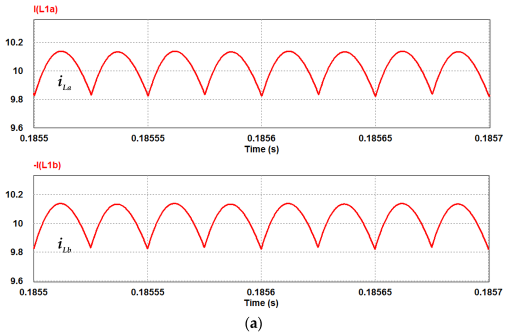
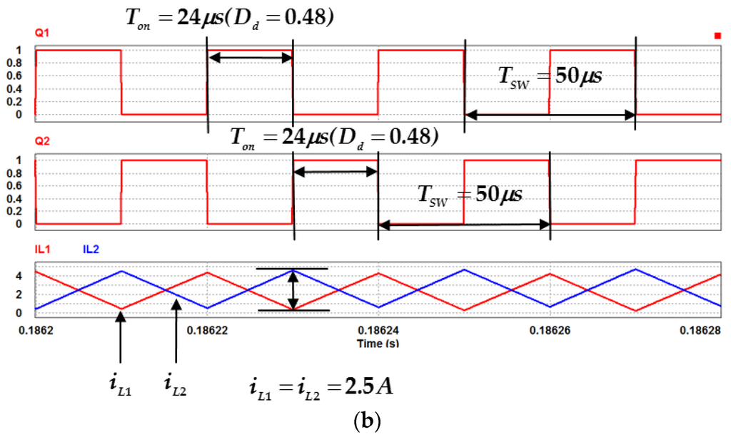
Figure 15.
Simulated waveforms of the studied BDC in charge state at full load: (a) low-side filter currents iLa, iLb; (b) gate signals of Q1, Q2 and two-phase inductor currents iL1, iL2.

Figure 16.
Measured waveforms of the studied BDC in charge state at full load: (a) low-side filter currents iLa, iLb; (b) gate signals of Q1, Q2 and two-phase inductor currents iL1, iL2.
Figure 17 and Figure 18 show the simulated and measured waveforms of charge-pump capacitor voltage (VCB), middle-link voltage (VM), middle-link capacitor voltages (VM1, VM2), low-side voltage (VL), and low-side switch voltages (VS1, VS2, VS3, VS4). From Figure 17 and Figure 18, with the ULC of studied BDC, the low-voltage side (VL) is well regulated at 48 V. The middle-link voltage is 96 V, it does quite reach twice of the regulated low-side voltage (VL) of 48 V. The charge-pump capacitor voltage (VCB) of 192 V can be achieved easily and indeed can share one-half of the high-side voltage to reduce the voltage stress of active switches. It is observed that the steady-state voltage stresses of low-side active switches (VS1, VS2, VS3, VS4) are only about 48 V, which means that lower on-resistance MOSFETs can be used to achieve the improved conversion efficiency. Also, both the simulated results are in close agreement with the corresponding experimental results.
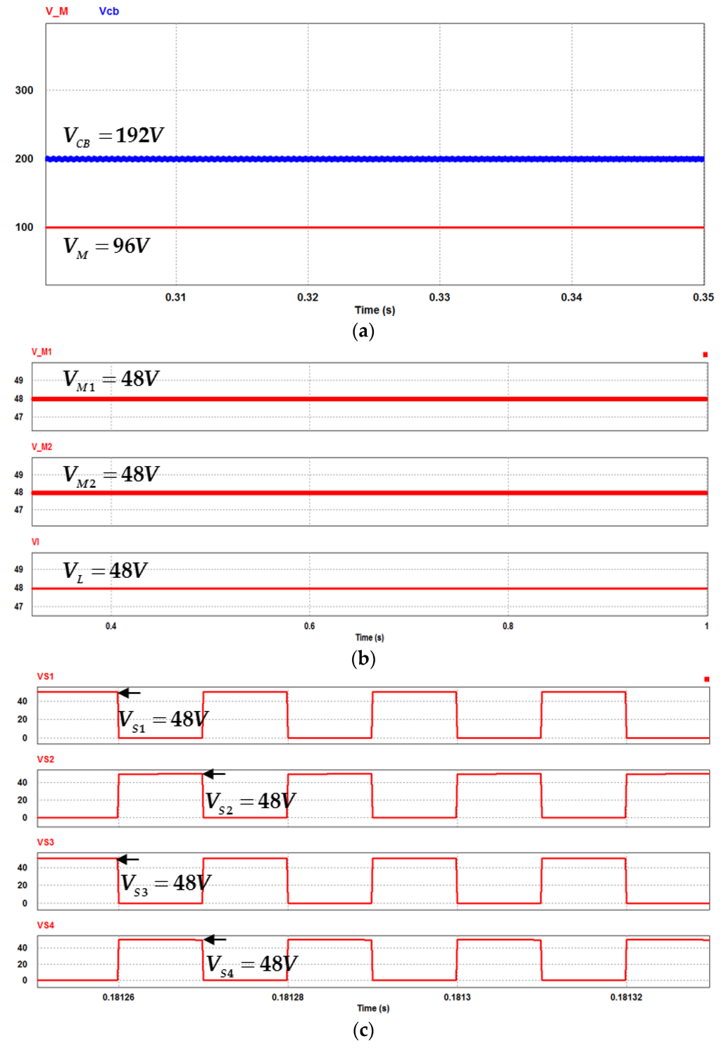
Figure 17.
Simulated waveforms of the studied BDC in charge state at full load: (a) charge-pump capacitor voltage VCB, middle-link voltage VM; (b) middle-link capacitor voltages VM1, VM2, and low-side voltage VL; (c) switch voltages of S1, S2, S3, S4.

Figure 18.
Measured waveforms of the studied BDC in charge state at full load: (a) charge-pump capacitor voltage VCB and middle-link voltage VM; (b) middle-link capacitor voltages VM1, VM2, and low-side voltage VL; (c) switch voltages of S1, S2, S3, S4.
Figure 19 shows the simulated waveforms of gate signals of Q3, Q4, the two-phase inductor currents (iL1, iL2) and the switch voltages of (VQ3, VQ4) in charge state at full load condition. The corresponding experimental results are also shown in Figure 20. One can observe that both results are in very close agreement as well. From the figures it is observed that by interleaved controlling the duty cycles of 0.52 for the switches (Q3, Q4), the two-phase currents (iL1, iL2) are in complementary relation and in CCM. Also, from Figure 19b and Figure 20b, the charge-pump capacitor voltage (VCB) is about 192.5 V, it can clamp the switch voltages of active switches (Q3, Q4) to be nearly one-half of the regulated high-side voltage VH of 385 V.
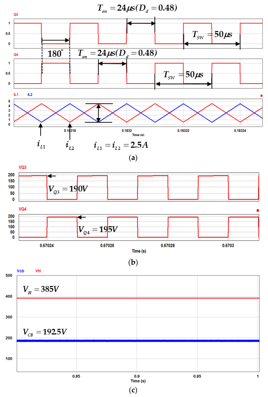
Figure 19.
Simulated waveforms of the studied BDC in discharge state at full load: (a) gate signals of Q3, Q4, two-phase inductor currents iL1, iL2; (b) switch voltages of Q3, Q4; (c) charge-pump capacitor voltage VCB and high-side voltage VH.
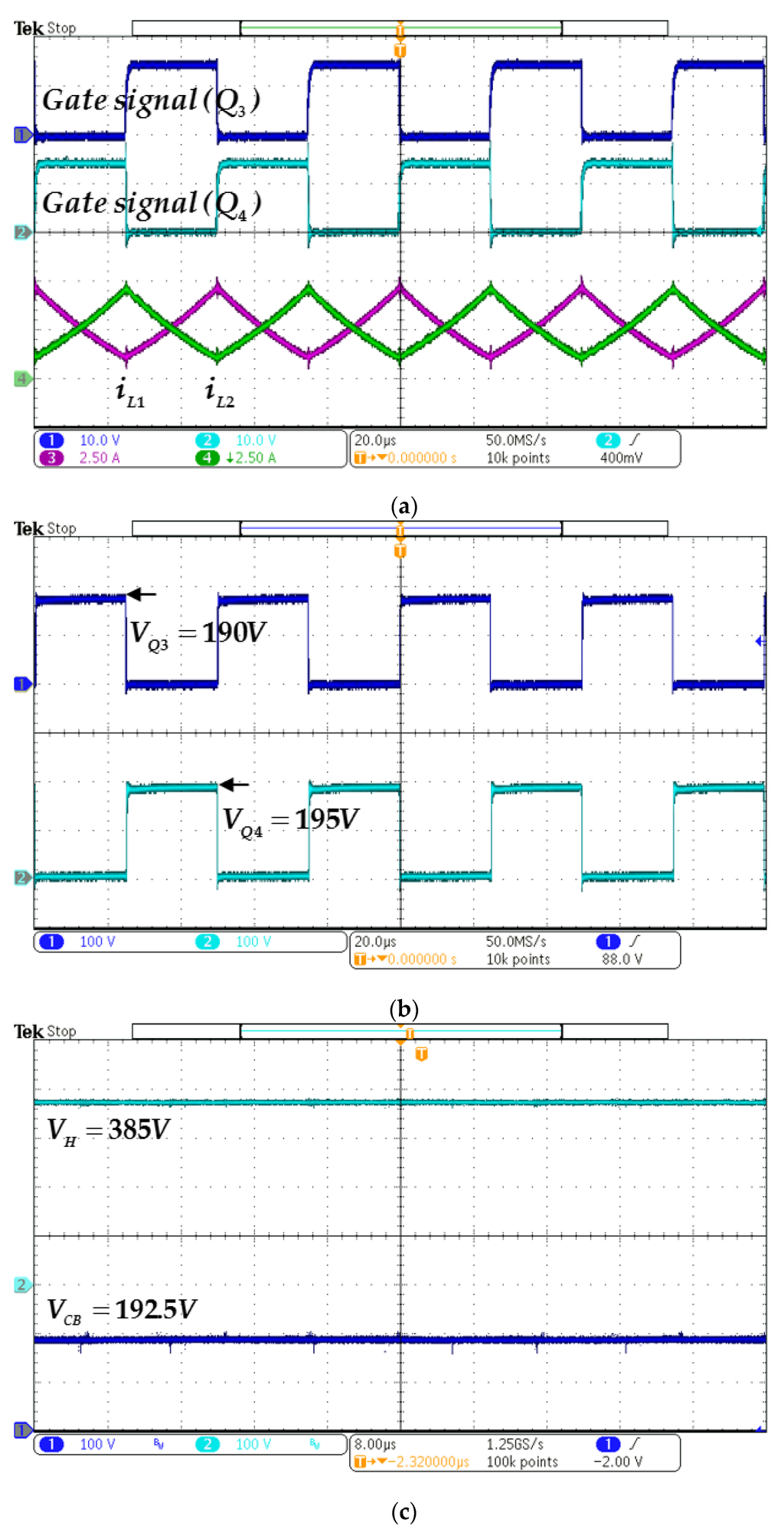
Figure 20.
Measured waveforms of the studied BDC in discharge state at full load: (a) gate signals of Q3, Q4, two-phase inductor currents iL1, iL2; (b) switches voltages of Q3, Q4; (c) charge-pump capacitor voltage VCB and high-side voltage VH.
Figure 21 summarizes the measured conversion efficiency of the studied BDC in charge and discharge states. On the experimental porotype system, the conversion efficiency is measured via precise digital power meter WT310 equipment, manufactured by the Yokogawa Electric Corporation (Tokyo, Japan). The accuracy of the measured power is within +/−0.1%. It can be seen that from Figure 21, the measured highest conversion efficiency is 95% in discharge state and is around 96% in charge state. In order to clarify the actual measured conversion efficiency further, based on the equations in Table 2, the calculated power loss distribution at the rated load condition is listed in Table 3, and furthermore, the calculated losses breakdown diagrams of the studied BDC are depicted in Figure 22. From Table 3 and Figure 22, one can see that the power losses mainly occur in the copper loss of the inductors, switching loss and conduction loss of the MOSFETs. The total power losses in charge and discharge states are 28.5 W and 28.6 W, accounting for 5.70% and 5.73%, in rated load condition, respectively. These match well the measured conversion efficiency of the studied BDC in charge (94.29%) and discharge (94.25%) states.
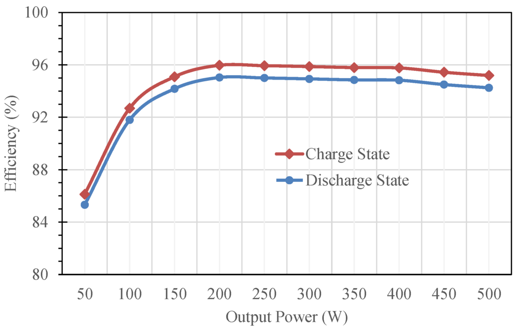
Figure 21.
Measured conversion efficiency of the studied BDC for low-side voltage VL = 48 V and high-side voltage VH = 385 V under different loads.

Table 3.
Power loss distribution (500 W rated load condition).

Figure 22.
Calculated losses breakdown diagrams at rated load condition: (a) in charge state; (b) in discharge state.
The performance comparisons between the studied BDC and a variety of published research results are summarized in Table 4. As can be seen from the comparative data, though the amounts of components in the proposed converter are more than the requirement in the other previous BDCs. The studied two-phase BDC indeed performs the higher conversion efficiency, bidirectional power flow, lower output ripples under 500 W power rating than other announced works [17,22,23]. Finally, the practical photograph of the realized BDC prototype and the test bench system are depicted in Figure 23.

Table 4.
Performance comparisons with other published converters.
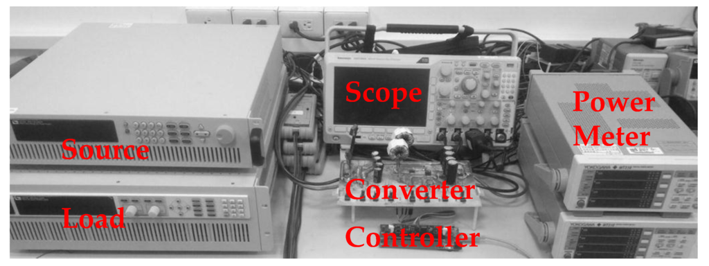
Figure 23.
Photograph of the realized BDC prototype and the test bench system.
5. Conclusions
A novel BDC topology with high voltage conversion ratio is developed and a 500 W rating prototype system with 48 V battery input is constructed. Applying the developed BDC topology to the 48 V mini-hybrid powertrain system is also expected in the future [27]. In this study, thanks to the ULC located at the low-side stage, high power density and efficiency in all load range make the studied BDC a promising two-stage power architecture. Furthermore, the IBCPC located at the high-side stage can achieve a much higher voltage conversion ratio under a reasonable duty cycle. In summary, the proposed novel BDC offers the following improvements: (1) high voltage conversion ratio; (2) low ripple current; (3) it is simpler to design, implement and control. Finally, a 500 W rating low-power prototype system is given as an example for verifying the validity of the operation principle. Experimental results show that a highest efficiency of 96% and 95% can be achieved, respectively, in charge and discharge states. Certainly, by making a suitable printed circuit board (PCB) layout, and with good component placement and good heat dissipation transfer process, the novel BDC can be implemented for higher power conversion applications.
Acknowledgments
This research is sponsored by the Ministry of Science and Technology, Taiwan, under contracts 104-2221-E-027-125, 104-2623-E-027-005-ET, and 104-2622-E-027-023-CC3. The author would like to thank the student, Jie-Ting Li for for his help in the experiment and Dr. Yuan-Chih Lin for his suggestions.
Conflicts of Interest
The author declares no conflict of interest.
References
- Lai, C.M.; Pan, C.T.; Cheng, M.C. High-efficiency modular high step-up interleaved boost converter for dc-microgrid applications. IEEE Trans. Ind. Appl. 2012, 48, 161–171. [Google Scholar] [CrossRef]
- Boroyevich, D.; Cvetkovic, I.; Burgos, R.; Dong, D. Intergrid: A future electronic energy network? IEEE J. Emerg. Sel. Top. Power Electron. 2013, 1, 127–138. [Google Scholar] [CrossRef]
- Yilmaz, M.; Krein, P.T. Review of the impact of vehicle-to-grid technologies on distribution systems and utility interfaces. IEEE Trans. Power Electron. 2013, 28, 5673–5689. [Google Scholar] [CrossRef]
- Lai, C.M.; Lin, Y.C.; Lee, D.S. Study and implementation of a two-phase interleaved bidirectional DC/DC converter for vehicle and dc-microgrid systems. Energies 2015, 8, 9969–9991. [Google Scholar] [CrossRef]
- Takeda, T.; Miyoshi, H.; Yukita, K.; Goto, Y.; Ichiyanagi, K. Power interchange by the DC bus in micro grids. In Proceedings of the IEEE International Conference on DC Microgrids, Atlanta, GA, USA, 7–10 June 2015; pp. 135–137.
- Wunder, B.; Ott, L.; Kaiser, J.; Han, Y.; Fersterra, F.; Marz, M. Overview of different topologies and control strategies for DC micro grids. In Proceedings of the IEEE International Conference on DC Microgrids, Atlanta, GA, USA, 7–10 June 2015; pp. 349–354.
- Hu, K.W.; Liaw, C.M. Incorporated operation control of DC microgrid and electric vehicle. IEEE Trans. Ind. Electron. 2016, 63, 202–215. [Google Scholar] [CrossRef]
- Du, Y.; Lukic, S.; Jacobson, B.; Huang, A. Review of high power isolated bi-directional DC-DC converters for PHEV/EV DC charging infrastructure. In Proceedings of the IEEE Energy Conversion Congress and Exposition, Phoenix, AZ, USA, 17–22 September 2011; pp. 553–560.
- Zhao, B.; Song, Q.; Liu, W.; Sun, Y. Overview of dual-active-bridge isolated bidirectional DC-DC converter for high-frequency-link power-conversion system. IEEE Trans. Power Electron. 2014, 29, 4091–4106. [Google Scholar] [CrossRef]
- Wai, R.J.; Liaw, J.J. High-efficiency-isolated single-input multiple-output bidirectional converter. IEEE Trans. Power Electron. 2015, 30, 4914–4930. [Google Scholar] [CrossRef]
- Du, Y.; Zhou, X.; Bai, S.; Lukic, S.; Huang, A. Review of non-isolated bi-directional DC-DC converters for plug-in hybrid electric vehicle charge station application at municipal parking decks. In Proceedings of the IEEE Applied Power Electronics Conference and Exposition, Palm Springs, CA, USA, 21–25 February 2010; pp. 1145–1151.
- Wai, R.J.; Duan, R.Y. High-efficiency bidirectional converter for power sources with great voltage diversity. IEEE Trans. Power Electron. 1997, 22, 1986–1996. [Google Scholar] [CrossRef]
- Wai, R.J.; Duan, R.Y.; Jheng, K.H. High-efficiency bidirectional DC-DC converter with high-voltage gain. IET Power Electron. 2012, 5, 173–184. [Google Scholar] [CrossRef]
- Yang, L.S.; Liang, T.J. Analysis and implementation of a novel bidirectional DC-DC converter. IEEE Trans. Ind. Electron. 2012, 59, 422–434. [Google Scholar] [CrossRef]
- Jiang, L.; Mi, C.; Li, S.; Zhang, M.; Zhang, X.; Yin, C. A novel soft-switching bidirectional DC-DC converter with coupled inductors. IEEE Trans. Ind. Appl. 2013, 49, 2730–2740. [Google Scholar] [CrossRef]
- Hsieh, Y.P.; Chen, J.F.; Yang, L.S.; Wu, C.Y.; Liu, W.S. High-conversion-ratio bidirectional DC-DC converter with coupled inductor. IEEE Trans. Ind. Electron. 2014, 61, 210–222. [Google Scholar] [CrossRef]
- Liang, T.J.; Liang, H.H.; Chen, S.M.; Chen, J.F.; Yang, L.S. Analysis, design, and implementation of a bidirectional double-boost DC-DC converter. IEEE Trans. Ind. Appl. 2014, 50, 3955–3962. [Google Scholar] [CrossRef]
- Chen, L.R.; Chu, N.Y.; Wang, C.S.; Liang, R.H. Design of a reflex-based bidirectional converter with the energy recovery function. IEEE Trans. Ind. Electron. 2008, 55, 3022–3029. [Google Scholar] [CrossRef]
- Han, D.; Noppakunkajorn, J.; Sarlioglu, B. Comprehensive efficiency, weight, and volume comparison of SiC- and Si-based bidirectional DC-DC converters for hybrid electric vehicles. IEEE Trans. Veh. Technol. 2014, 63, 3001–3010. [Google Scholar] [CrossRef]
- Jin, K.; Yang, M.; Ruan, X.; Xu, M. Three-level bidirectional converter for fuel-cell/battery hybrid power system. IEEE Trans. Ind. Electron. 2010, 57, 1976–1986. [Google Scholar] [CrossRef]
- Monge, S.B.; Alepuz, S.; Bordonau, J. A bidirectional multilevel boost-buck DC-DC converter. IEEE Trans. Power Electron. 2011, 26, 2172–2183. [Google Scholar] [CrossRef]
- Lin, C.C.; Yang, L.S.; Wu, G.W. Study of a non-isolated bidirectional DC-DC converter. IET Power Electron. 2013, 6, 30–37. [Google Scholar] [CrossRef]
- Ardi, H.; Ahrabi, R.R.; Ravadanegh, S.N. Non-isolated bidirectional DC-DC converter analysis and implementation. IET Power Electron. 2014, 7, 3033–3044. [Google Scholar] [CrossRef]
- Kabalo, M.; Paire, D.; Blunier, B.; Bouquain, D.; Simoes, M.G.; Miraoui, A. Experimental validation of high-voltage-ratio low input-current-ripple converters for hybrid fuel cell supercapacitor systems. IEEE Trans. Veh. Technol. 2012, 61, 3430–3440. [Google Scholar] [CrossRef]
- Lai, C.M.; Yang, M.J. A high-gain three-port power converter with fuel cell, battery sources and stacked output for hybrid electric vehicles and DC-microgrids. Energies 2016, 9, 180. [Google Scholar] [CrossRef]
- MOSFET Basics. Available online: https://www.fairchildsemi.com/application-notes/AN/AN-9010.pdf (accessed on 10 April 2016).
- Sattler, M.; Smetana, T.; Meyerhofer, T.; Kuhlkamp, L. 48 V minihybrid—A new solution for the minimale hybridization of vehicles. In Proceedings of the 22nd Aachen Colloquium Automobile and Engine Technology, Germany, 8 October 2013; pp. 995–1008.
© 2016 by the author; licensee MDPI, Basel, Switzerland. This article is an open access article distributed under the terms and conditions of the Creative Commons Attribution (CC-BY) license (http://creativecommons.org/licenses/by/4.0/).