Abstract
In order to understand the effect of Pb-CuI co-doping on the thermoelectric performance of Bi2Te3, n-type Bi2Te3 co-doped with x at % CuI and 1/2x at % Pb (x = 0, 0.01, 0.03, 0.05, 0.07, and 0.10) were prepared via high temperature solid state reaction and consolidated using spark plasma sintering. Electron and thermal transport properties, i.e., electrical conductivity, carrier concentration, Hall mobility, Seebeck coefficient, and thermal conductivity, of CuI-Pb co-doped Bi2Te3 were measured in the temperature range from 300 K to 523 K, and compared to corresponding x% of CuI-doped Bi2Te3 and undoped Bi2Te3. The addition of a small amount of Pb significantly decreased the carrier concentration, which could be attributed to the holes from Pb atoms, thus the CuI-Pb co-doped samples show a lower electrical conductivity and a higher Seebeck coefficient when compared to CuI-doped samples with similar x values. The incorporation of Pb into CuI-doped Bi2Te3 rarely changed the power factor because of the trade-off relationship between the electrical conductivity and the Seebeck coefficient. The total thermal conductivity(κtot) of co-doped samples (κtot ~ 1.4 W/m∙K at 300 K) is slightly lower than that of 1% CuI-doped Bi2Te3 (κtot ~ 1.5 W/m∙K at 300 K) and undoped Bi2Te3 (κtot ~ 1.6 W/m∙K at 300 K) due to the alloy scattering. The 1% CuI-Pb co-doped Bi2Te3 sample shows the highest ZT value of 0.96 at 370 K. All data on electrical and thermal transport properties suggest that the thermoelectric properties of Bi2Te3 and its operating temperature can be controlled by co-doping.
1. Introduction
Bismuth telluride (Bi2Te3) has been the focus of extensive theoretical and experimental studies as a component of materials for thermoelectric (TE) devices, such as solid-state coolers or generators [1,2,3]. The performance of a thermoelectric material in the aforementioned applications is evaluated in terms of a dimensionless figure of merit ZT, which is defined as (S2σ/κ)T; where S is the Seebeck coefficient (or thermopower), σ is the electrical conductivity, κ is the thermal conductivity, and T is the temperature [4]. The product (S2σ) is called the power factor. A larger ZT leads directly to a higher conversion efficiency. The main challenge lies in the decoupling of the interdependent thermoelectric parameters (S, σ, and κ), which are strongly coupled to the carrier concentration. Commercial TE devices comprise series of p- and n-type semiconductor pairs.
The ZT values of commercial Bi2Te3 compounds are about 1.35 for p-type and 0.9 for n-type materials [5]. The poor performance of n-type Bi2Te3 based materials compared to that of p-type materials seriously inflicts a limitation on making it a more efficient TE device. Both p-type and n-type characteristics of Bi2Te3 can be controlled depending on the chemical composition. As is well known, n-type Bi2Te3 have been synthesized by making solid solution with Bi2Se3, or addition of excess tellurium as an electron donor [6,7]. However, the fabrication of n-type Bi2Te3 thermoelectric materials has a number of technical problems, such as controlling the Se content in Bi2Te3-Bi2Se3 solid solution is difficult and Te-rich Bi2Te3 easily decomposes upon heating. Element doping is a more effective approach to enhance the thermoelectric properties of Bi2Te3-based alloys [8,9,10,11,12]. Among various dopants, Cu or Cu-halide acts as an excellent additive for improvement of thermoelectric performance of n-type Bi2Te3 [13,14,15,16]. Cu atoms can be either an acceptor or a donor depending on their location in the compound. Cu is also known to improve the reproducibility of thermoelectric materials, due to the formation of Cu–Te bond in the van der Waals gaps, which suppress the escape of Te atoms [17]. The Cu-intercalated Bi2Te3 bulk shows a significantly enhanced ZT of ~1.12 at 300 K [13], which is the highest ZT value reported for n-type Bi2Te3 binary material. Cu addition can also prevent the oxidation of the Bi2Te3 [17]. However, the thermoelectric properties of these alloys change with aging time [18]. Studies of the structure and properties of crystals with a co-dopant with Cu content were carried out [16,19,20]. Cu and I atoms co-doped Bi2Te3 was prepared using the Bridgman method for the improvement of its corresponding thermoelectric properties, whereby the power factor was improved through the co-doping effect of Cu and I, while its thermal conductivity was reduced by forming dispersed Cu-rich nanoprecipitates. The maximum ZT of ~1.16 was achieved at a temperature of 368 K for (CuI)0.01Bi2Te3 [16]. Moreover, various dopants (Au, Mn, Co, Ni, Zn, Ge, Ag, In, Sc, Ti, V, and Sn) in Cu0.008Bi2Te2.7Se0.3 have been studied [19,20]. The addition of dopant atoms at Bi sites in n-type Cu-intercalated Bi2Te3 changes the electronic band structure, such as band position and band degeneracies, resulting in an increase of the Seebeck coefficient. As a consequence, peak ZT values of 0.88 at 360 K and 0.91 at 320 K were obtained for V-doped and Au-doped Cu0.008Bi1.98Te2.7Se0.3, respectively [19,20]. Therefore, it has great potential to further improve the ZT value of n-type Bi2Te3 based materials via compositional tuning approach by adjusting Cu contents or element doping.
In the present study, CuI-Pb co-doped Bi2Te3 samples were prepared using high temperature solid state reaction method and were consolidated by spark plasma sintering (SPS). The Pb-addition effects on the crystal lattice, the charge transport, and the thermoelectric properties of CuI-doped Bi2Te3 were evaluated.
2. Results and Discussion
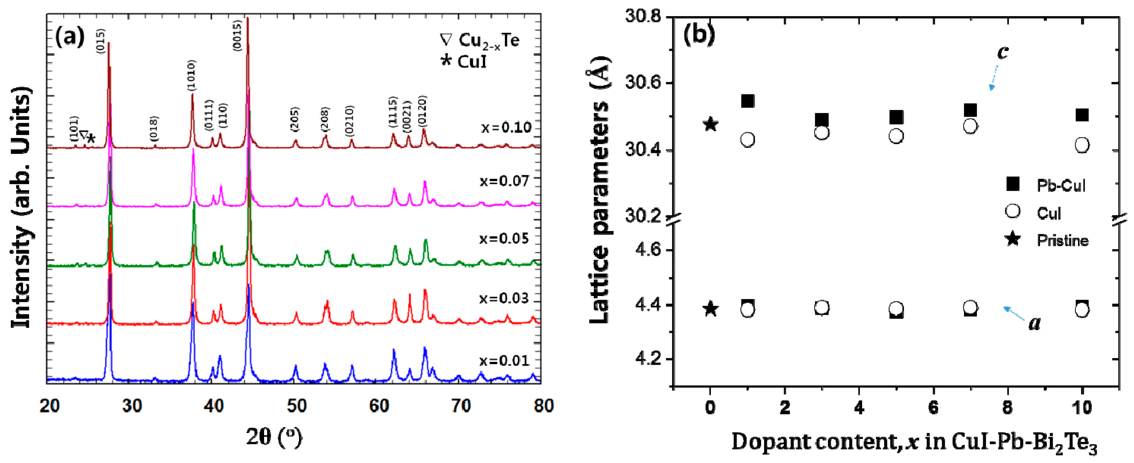
Powder X-ray diffraction (PXRD) patterns of x% CuI-Pb co-doped Bi2Te3 (x = 0.01, 0.03, 0.05, 0.07, and 0.10) samples are shown in Figure 1a. As a comparison, undoped Bi2Te3 and x% CuI-doped Bi2Te3 were prepared under the same synthetic conditions. All of the diffraction peaks are indexed to rhombohedral Bi2Te3 structure with the space group of R3m (JCPDS, No. 15-0863) [21], with no indication for the existence of a second phase for samples with up to 7% of dopant concentration. Trace amounts of possible impurities including Cu2−xTe, and CuI were detected in the 10% CuI-Pb co-doped Bi2Te3 samples. This result implies that the solubility limit of CuI and Pb dopants in Bi2Te3 was x < 0.1. While in a previous report, the impurity phase was observed in less than 5% in CuI-doped Bi2Te3 sample [16], when Pb atoms are co-doped with CuI in Bi2Te3, the impurity phase was observed only in a 10% CuI-Pb co-doped Bi2Te3 sample. This result indicates that the solubility of CuI in Bi2Te3 is increased by addition of Pb atoms. Figure 1b shows the lattice parameters of CuI-Pb co-doped and CuI-doped Bi2Te3 samples as a function of the dopant fraction. In all of the samples, the in-plane parameter a remains constant, while the unit cell parameter c along the stacking direction expands with an increasing Pb content in the CuI-Bi2Te3 system. The result is presumably a consequence of Cu atoms entering into the interstitial site, which increases the distance between the van der Waals layers [13]. A comparison of the covalent radius of Pb (rPb = 0.147 nm) with that of Bi (rBi = 0.146 nm) shows that the size of Pb is very close to that of Bi, and thus the ability of Pb atoms for the substitution of Bi atoms in Bi2Te3 should not be neglected. Halogen atoms such as I (rI = 0.220 nm) are believed to occupy Te (rTe = 0.221 nm) sites in the lattice [22]. The incorporation of iodine atoms to Te sites and Pb atoms to Bi sites drive the changes in bonding parameters. The substituted atoms can bridge two neighboring quintuple layers, thus weakening the interface scattering. Such an analysis exceeds the scope of this paper and would demand quantum chemical calculations of bonding parameters, which will be the aim of our next work.

Figure 1.
(a) Powder X-ray diffraction (XRD) patterns of samples of x% CuI-Pb co-doped Bi2Te3 (x = 0.01, 0.03, 0.05, 0.07, and 0.10) with peaks of impurity phases (marked by symbols (∇ and *)); (b) Lattice parameters of samples of x% CuI-Pb co-doped Bi2Te3 (x = 0, 0.01, 0.03, 0.05, 0.07, and 0.10).
In our previous work, we demonstrated that doping of Bi2Te3 samples with 1% CuI enhanced ZT [16]. Thus, we selected 1% CuI-doped Bi2Te3 sample as a reference material to demonstrate the effect of CuI-Pb co-doping on the charge transport properties. The charge transport properties of 1% CuI-Pb co-doping Bi2Te3 at room temperature are investigated by Hall effect analysis and are compared to those of 1% CuI-doped Bi2Te3 and undoped Bi2Te3. Assuming one carrier type and parabolic bands in our analysis, the carrier concentration (n) was calculated from the room temperature (i.e., well within a single-carrier dominated transport) Hall constants using the relationship RH = 1/ne, where RH is the Hall coefficient, n is the carrier concentration, and e is the electronic charge. The Hall coefficients of specimens are negative, indicating n-type conductions. By incorporating Pb in CuI- Bi2Te3 system, the ne value of the bulk samples decreases from ~7.8 × 10¹⁹/cm3 (CuI-doped Bi2Te3) to ~3.6 × 10¹⁹/cm3 (CuI-Pb co-doped Bi2Te3), and the corresponding mobility value increases from ~164.6 cm2/V∙s to ~216.9 cm2/V∙s at 300 K. In comparison, the undoped Bi2Te3 sample shows the n value of ~1.2 × 10¹⁹/cm3and the mobility of 354.9 cm2/V∙s at 300 K. This result verifies that the addition of a small amount of Pb significantly decreases the carrier concentration, which should be attributed to the holes generated by the Pb atoms. This demonstrates that facile control of electron concentration can be easily realized by adding Pb atoms to CuI-doped Bi2Te3 system, yielding an optimal electron concentration of 3−4.5 × 10¹⁹/cm3.
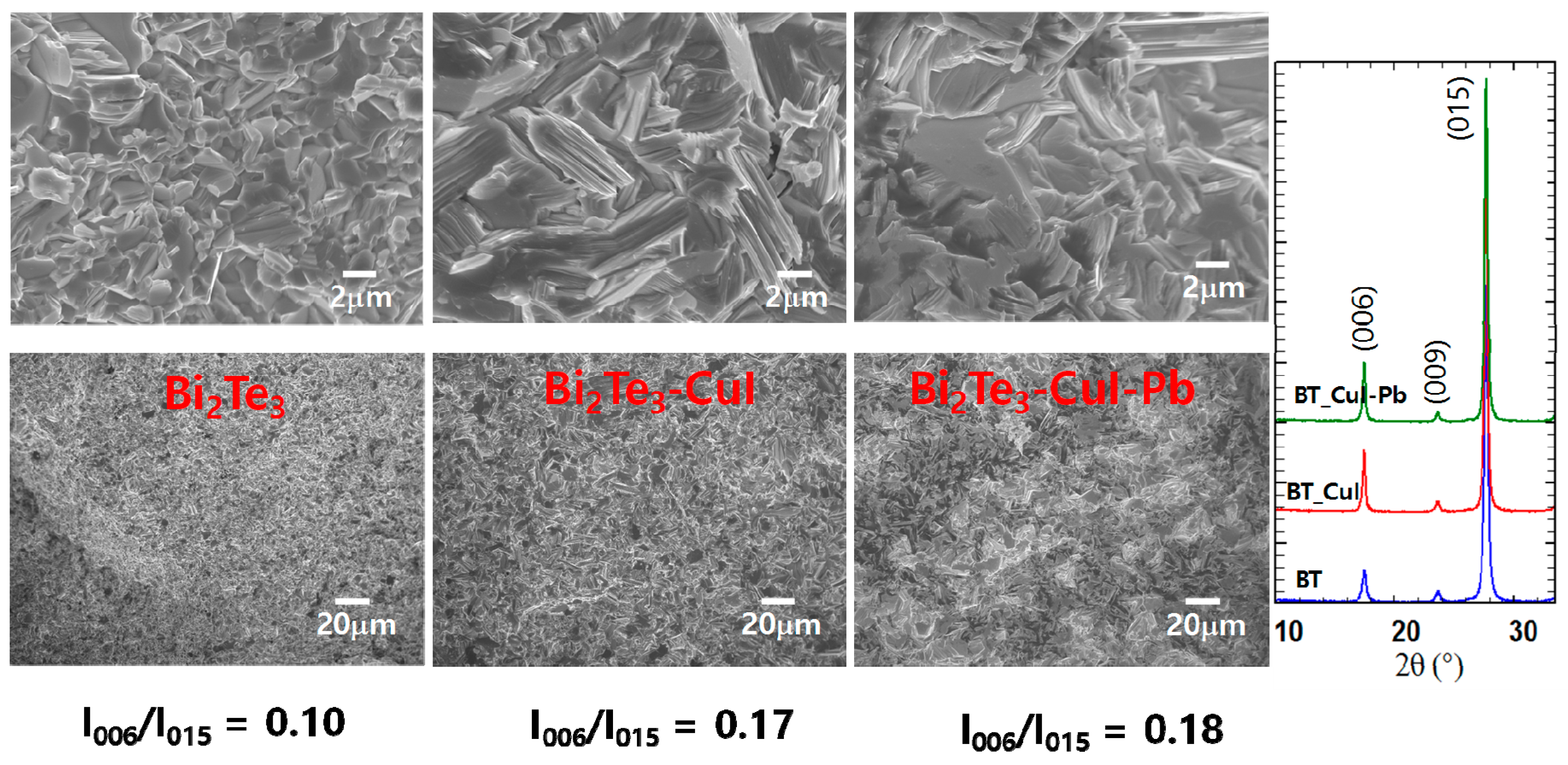
Figure 2a shows SEM images of the fractured surfaces of SPSed undoped Bi2Te3, 1% CuI-doped Bi2Te3, and 1% CuI-Pb co-doped Bi2Te3. All of the samples exhibit lamellar structures at the micron scale and no obvious large-scale preferred orientation. The microstructures are dense (>98% of the theoretical density of n-type Bi2Te3 (7.86 g/cm3) showing densities of 7.73 g/cm3, 7.77 g/cm3, and 7.82 g/cm3 for undoped Bi2Te3, 1% CuI-doped Bi2Te3, and 1% CuI-Pb co-doped Bi2Te3, respectively. The orientation degree of the (0 0 l) planes, termed as F, was calculated with the Lotgering method [23]. In this method, F is expressed as the following equations: F = P − P0/1 − P0, P0 = I0(0 0 l)/∑I0(h k l), P = I(0 0 l)/∑I(h k l), where I0(0 0 l) is the intensity of (0 0 l) peaks and ∑I0(h k l) is the sum of intensities of all the peaks for the powders with random orientation; I(0 0 l) is the (0 0 l) peak intensity and ∑I(h k l) is the sum of the intensities of all peaks for the measured section. We calculated the ratios I(0015)/I(015) of the integrated intensity of (0015) to (015), and represented them in Figure 2b to evaluate the grain orientation anisotropy. All of the samples show anisotropy in the crystal structure; however, the degree of anisotropic orientation is not significant in SPS consolidated polycrystalline samples. The I(0015)/I(015) value for 1% CuI-doped Bi2Te3 and 1% CuI-Pb co-doped Bi2Te3 (17–18%) is slightly higher than those for undoped Bi2Te3 (10%). This indicates that the c-axis of the grains after SPS was preferentially oriented parallel to the pressing direction. This result is consistent with a previous report [16], showing the strengthening of the two adjacent quintuple layers by substituting Te with I atoms. Effect caused by sample density or sample orientation is negligible since the relative densities and orientation degree determined by the Lotgering method for CuI-doped and CuI-Pb co-doped Bi2Te3 samples are nearly same.
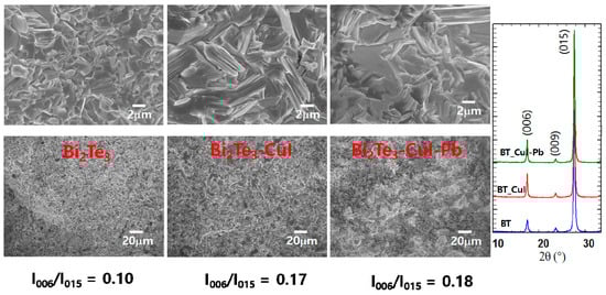
Figure 2.
SEM images, and XRD patterns of undoped Bi2Te3, 1% CuI-doped Bi2Te3, and 1% CuI-Pb co-doped Bi2Te3.
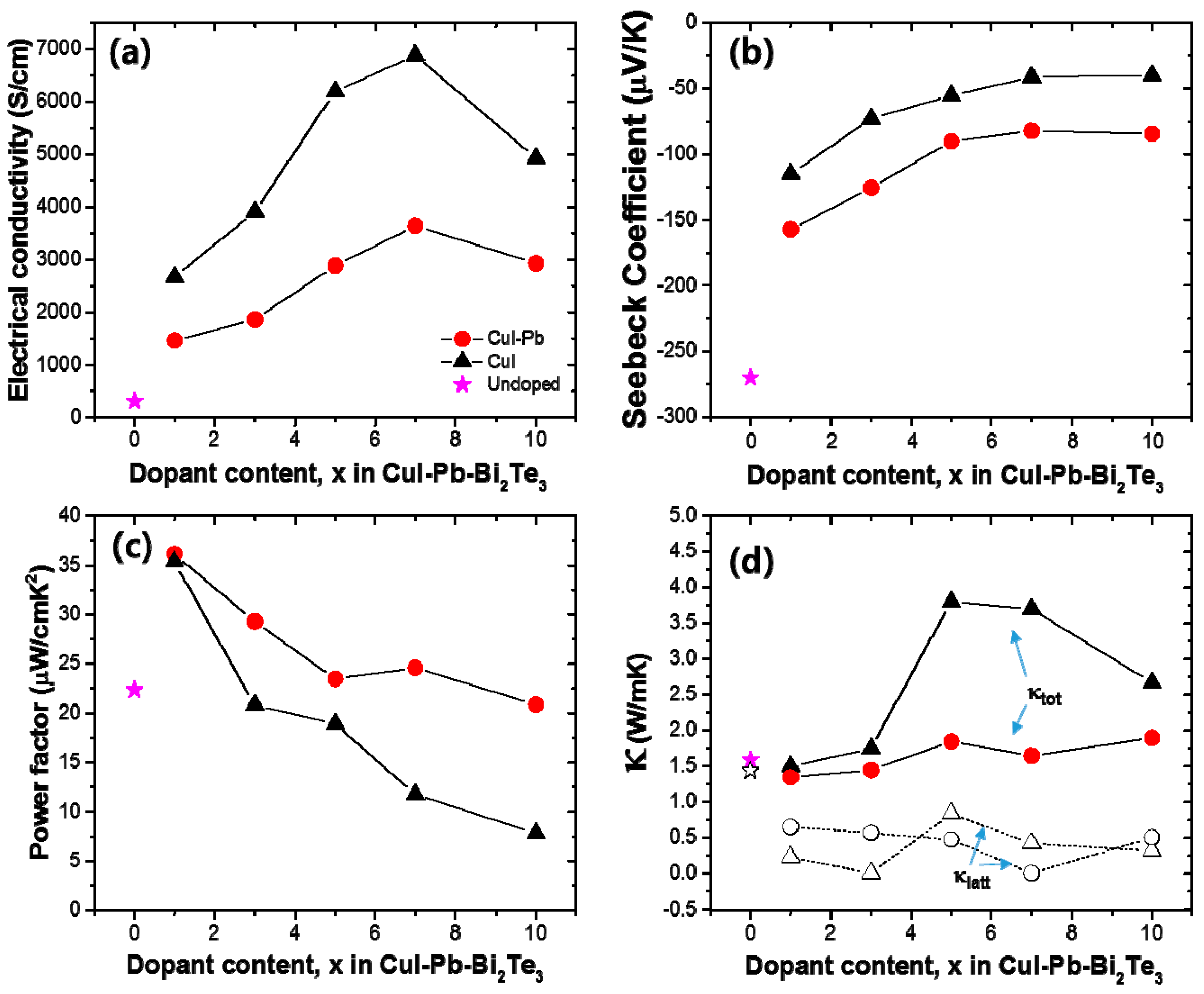
The thermoelectric properties depend on the dopants (here, we use CuI only and CuI-Pb), dopant content, and temperature. In order to elucidate the effect of dopants and their contents on the thermoelectric properties, the electrical conductivity (σ), Seebeck coefficient (S), and power factor of CuI-doped and CuI-Pb co-doped Bi2Te3 (x = 0, 0.01, 0.03, 0.05, 0.07, and 0.10) system as a function of composition was investigated at room temperature, as shown in Figure 3. In both series, with increasing dopant concentration, the electrical conductivity increase, while the Seebeck coefficient decreases simultaneously for up to 7% of dopant concentration. The room temperature electrical conductivity of the undoped Bi2Te3 (~307 S/cm) is increased by CuI-doping (1% of CuI-doped Bi2Te3 sample gave ~2673 S/cm). The room temperature electrical conductivity of 1% CuI-Pb co-doped Bi2Te3 at 300 K was about ~1462 S/cm. This value is significantly lower than that of 1% CuI-doped Bi2Te3. As shown in Figure 3a, the CuI-Pb co-doped samples show a lower electrical conductivity than that of CuI-doped samples with similar x values, confirming the role of Pb as an acceptor [24]. In Figure 3b, the Seebeck coefficients at room temperature were plotted as a function of dopant contents. The value of Seebeck coefficient at 300 K for CuI-doped and CuI-Pb co-doped Bi2Te3 are about −115 μV/K and −157 μV/K, respectively, while that for undoped Bi2Te3 is −270 μV/K, which compares well with the previous reported value for n-type Bi2Te3 [2]. The Seebeck coefficients of the CuI-Pb co-doped bulk samples are observed to be higher than that of the CuI-doped sample due to lower carrier concentrations. Normally, Bi2Te3 shows p-type character, however the undoped Bi2Te3 in this study show n-type character. We assume that these differences may arise from the different experimental conditions used for the preparation of undoped Bi2Te3 crystals. The Bi2Te3 prepared by the Bridgman method is a p-type conductor due to the antisite defect of BiTe. However, in this work, the SPS pressed Bi2Te3 samples show n-type characteristics, which arises from the Te vacancy at the interface. This decrease in electrical conductivity and the increase in Seebeck coefficient in co-doped samples can be explained by an increased carrier scattering related to the incorporation of Pb atoms in the CuI-doped lattice and by decreased carrier concentrations caused by Pb atoms, which act as electron acceptors [24]. As shown in Figure 3c, the CuI-Pb co-doped samples show higher power factors than CuI-doped samples with similar x values. The power factors decrease with increasing dopant concentrations. The maximum values of the power factors were observed at x = 0.01 for both CuI and CuI-Pb co-doped samples. The benefit of Pb incorporation into CuI-doped Bi2Te3 was not observed in the power factor because of the trade-off relationship between the Seebeck coefficient and the electrical conductivity. (~35 μW/cm∙ K2 for 1% CuI-doped Bi2Te3; ∼36 μW/cm∙K2 for 1% CuI-Pb co-doped Bi2Te3). This corresponds to an >80% enhancement over the typical value of undoped Bi2Te3 (22 μW/cm∙K2). Figure 3d represents thermal conductivities (closed symbols for κtot and open symbols for κlatt) as a function of dopant content. As the dopant concentration increased, the total conductivity of CuI-doped and CuI-Pb co-doped Bi2Te3 increased due to the increase of the electronic contribution. The total thermal conductivity κtot of 1% CuI-Pb co-doped samples (κtot ~ 1.4 W/m∙K at 300 K) is slightly lower than that of 1% CuI-doped Bi2Te3 (κtot ~ 1.5 W/m∙K at 300 K) and undoped Bi2Te3 (κtot ~ 1.6 W/m∙K at 300 K) due to alloy scattering. The lattice part (κlatt) of the thermal conductivity can be estimated by subtracting the electronic component (κelec) from the measured total thermal conductivity, κlatt = κtot − κelec. The electronic component is given by the Wiedemann-Franz relation, κelec = LσT, where L is the Lorenz number. L is taken to be 1.5 × 10⁻⁸ V2/K2 for near-degenerate or degenerate semiconductor [25,26]. The lattice thermal conductivity of 1% CuI-Pb co-doped Bi2Te3 was 0.66 W/m∙K at 300 K. In contrast to the behavior of κtot upon increasing the dopant concentration, κlatt slightly decreased with increasing dopant concentration. This result demonstrates clearly that the lattice κlatt is reduced by Pb incorporation through the alloy phonon scattering.
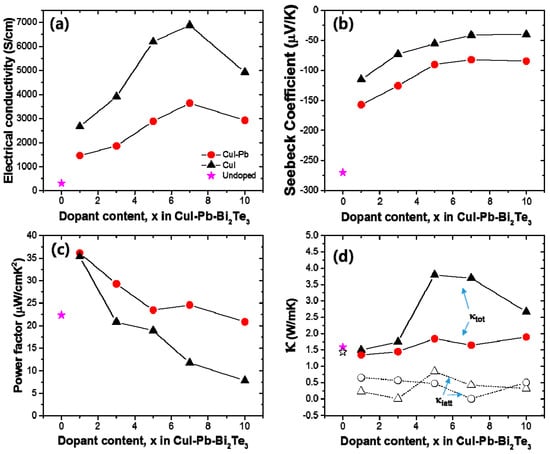
Figure 3.
(a) Electrical conductivity (σ); (b) Seebeck coefficient (S); (c) power factor; and (d) thermal conductivity as a function of dopant concentration x in the CuI-doped (black) and CuI-Pb co-doped Bi2Te3 (x = 0, 0.01, 0.03, 0.05, 0.07, and 0.10) system (red) at room temperature.
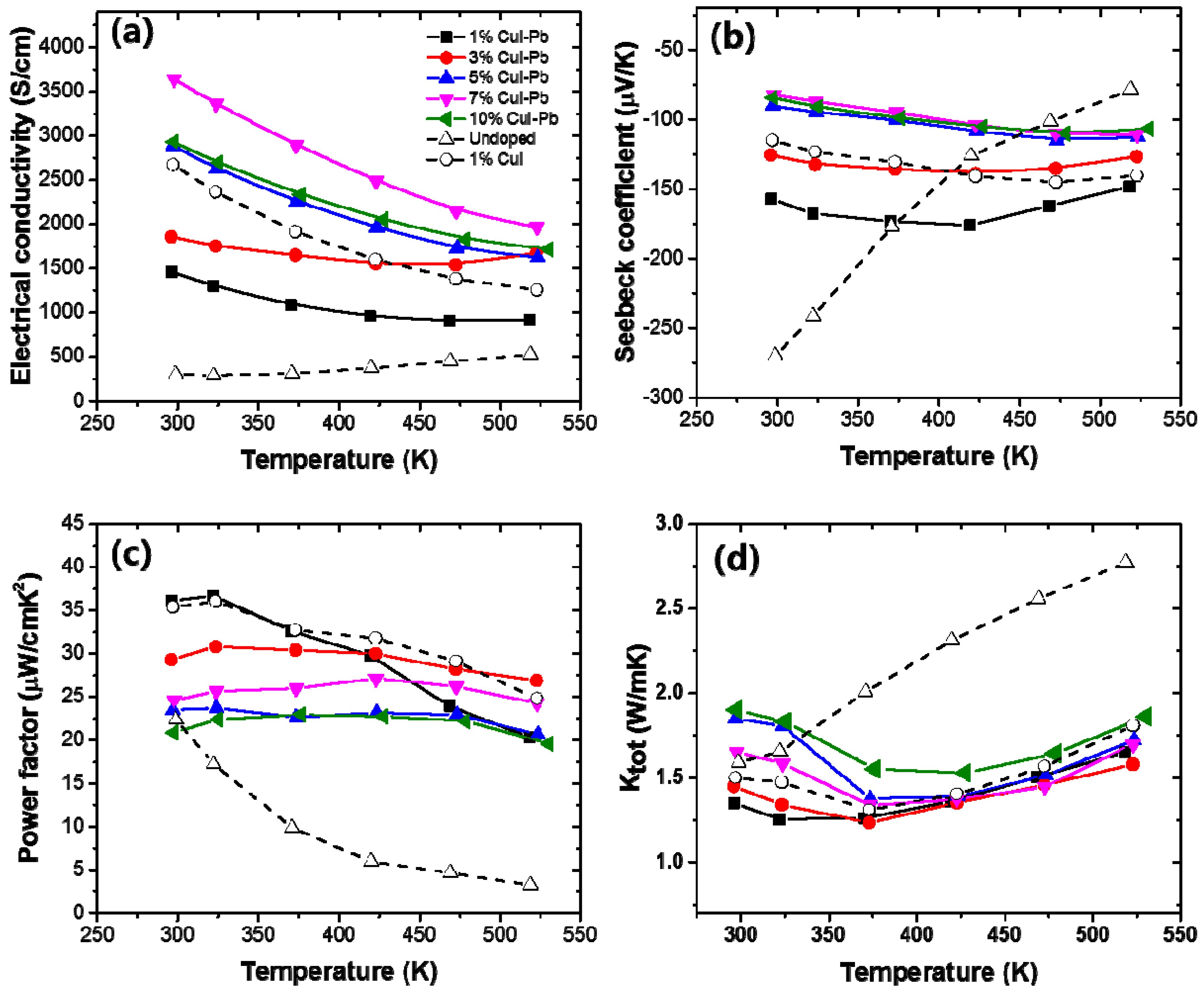
Figure 4 shows the electrical transport properties as a function of measured temperature of x% CuI-Pb co-doped Bi2Te3 (x = 0.01, 0.03, 0.05, 0.07, and 0.10), when compared with 1% CuI-doped Bi2Te3 and undoped Bi2Te3. For all of the samples, a monotonic decrease in electrical conductivity with increasing temperature is observed (Figure 4a), which is indicative of heavily degenerated doping. The variation of the Seebeck coefficient is similar to that of the electrical conductivity, as shown in Figure 4b. The Seebeck coefficient is negative in the whole temperature range, indicating that the majority of charge carriers are electrons (n-type). The magnitude of the Seebeck coefficient initially increases and reaches a maximum that is strongly depend on the Pb content x. The onset of intrinsic conduction (the maxima of the curves) in these samples shifts to a higher temperature with an increasing dopant content. While the x = 0% sample has its maxima at ~300 K, the 1% and 3% sample have their maximum at ~425 K, and the x > 5% sample at ~525 K. The maximum value of the Seebeck coefficient (~−176 μV/K) was observed at x = 0.01 CuI-Pb content at 425 K. Figure 4c shows the power factors (S2σ) values as a function of temperature. In this system, the power factor values for the 1% CuI-Pb co-doped ranged from 36 μW/cm·K2 at 300 K to 20 μW/cm·K2 at 523 K. The CuI-Pb co-doped sample with x > 0.03 shows a mild temperature dependence. Figure 4d shows the temperature dependence of the total thermal conductivity κtot of the samples. The κtot of all the doped samples firstly decreases due to the increasing phonon-phonon scattering, and then increases when upon further increase of the testing temperature due to the increase of ambipolar thermal contributions arising from the diffusion of electron-hole pairs with the onset of intrinsic contribution [27].
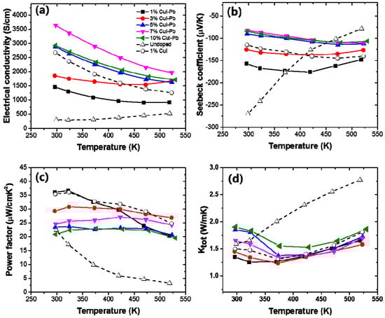
Figure 4.
The temperature dependence of (a) electrical conductivity (σ); (b) Seebeck coefficient (S); (c) power factor, and (d) thermal conductivity of x% CuI-Pb co-doped Bi2Te3 (x = 0.01, 0.03, 0.05, 0.07, and 0.10).
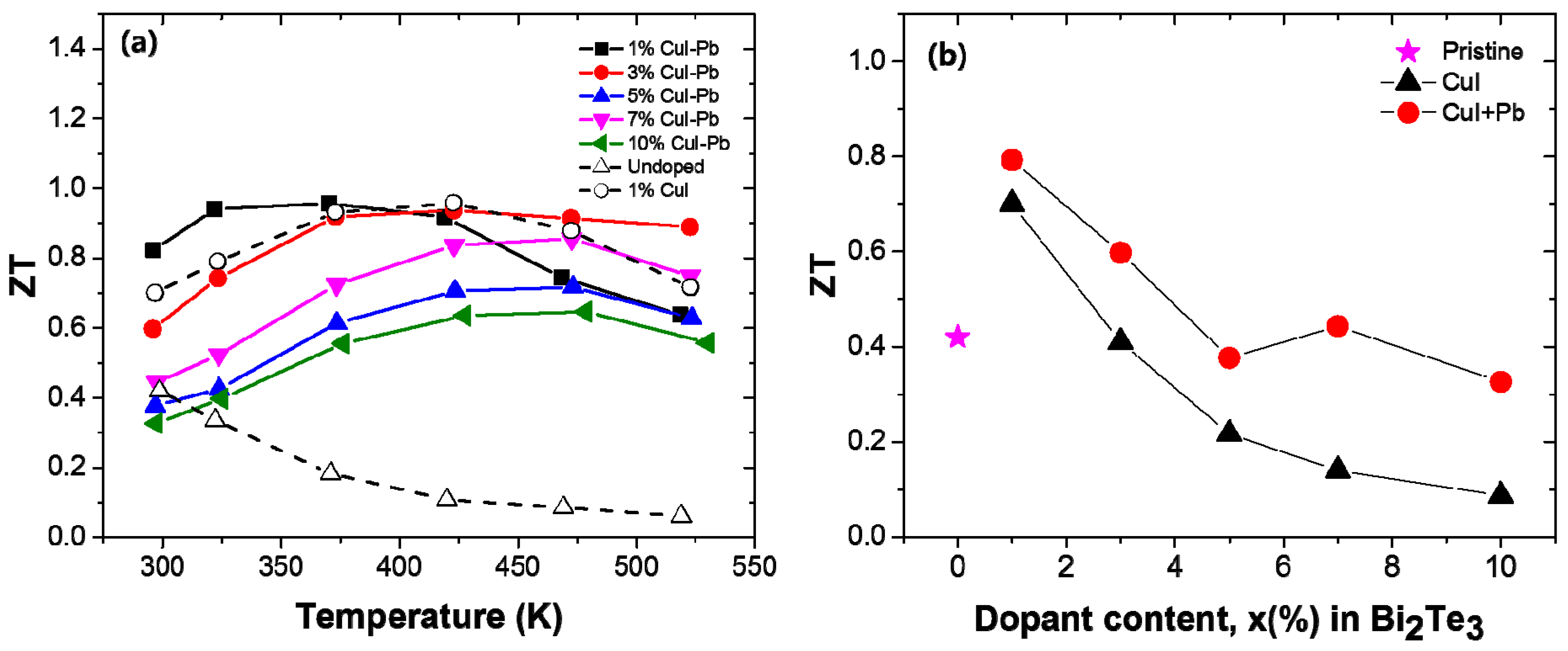
The dimensionless figure of merit ZT of the samples with different dopant concentration (x) are shown in Figure 5a as a function of temperature. The magnitude of the ZT initially increases and reaches a maximum that is strongly dependent on the dopant content x. When the temperature is above ~400 K, the ZT values decrease due to the appearance of intrinsic excitation at a higher temperature. In this experiment, the ZTmax of the 1% CuI-Pb co-doped sample was about 0.96 at 370 K, while the highest value ZTmax was about 0.96 at 422 K for the 1% CuI-doped sample. The incorporation of Pb into CuI-doped Bi2Te3 led to a shift of the peak position of ZTmax to lower temperatures. This result shows that the optimization of the operating temperature can be controlled by co-doping. For practical applications of thermoelectric materials, the ZT values at room temperature are also important. Figure 5b shows the room temperature ZT of the samples as a function of the dopant concentration. The undoped Bi2Te3 sample shows a low ZT of ~0.42 at 300 K due to its very poor electrical properties. The highest ZT of 0.79 and 0.70 at 300 K were achieved for the 1% CuI-Pb doped sample and 1% Cu-doped Bi2Te3 sample, respectively, which are both significantly improved when compared with those of the undoped sample. All of the evidences about electrical and thermal transport properties suggest that the n-type ZT of Bi2Te3 can be enhanced by the incorporation of Pb with CuI dopant. Further improvement in its TE properties can be expected by choosing suitable combination of dopants.
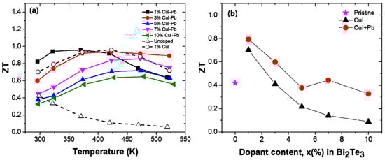
Figure 5.
(a) Temperature dependency; and (b) Dopant content dependency of the room temperature ZT for x% CuI-Pb co-doped Bi2Te3 (x = 0.01, 0.03, 0.05, 0.07, and 0.10), 1% CuI-doped Bi2Te3, and undoped Bi2Te3.
3. Materials and Methods
3.1. Synthesis of Bulk ingot and Powder Processing
n-type Bi2Te3 co-doped with x at % CuI and 1/2x at % Pb (x = 0, 0.01, 0.03, 0.05, 0.07, and 0.10) were prepared by means of the conventional high-temperature solid-state reaction method, using Bi, Te, CuI and Pb (All 99.999%, from Alfa Aesar, Ward Hill, MA, USA) as starting materials. For convenience, the samples are labeled as dopant contents, such as that Bi2Te3 + x CuI + 1/2x Pb with x is labeled as x% CuI-Pb co-doped Bi2Te3. n-type Bi2Te3 doped with x at % CuI alone was prepared under identical experimental conditions for comparison. The corresponding elements were sealed in appropriate ratio in evacuated fused silica tubes (14 mm diameter, 1 mm wall thickness) under a residual pressure of ~10−4 Torr. The sealed tubes were heated to 1000 °C over 12 h, and then held at 1000 °C for 12 h while rocking the liquid to facilitate a complete mixing of the contents. The tubes were slowly cooled to 800 °C over a period of 12 h and then quenched to room temperature. The cast ingot samples were powdered by ball milling in an Ar-filled glove box and the ground powder was passed through a 53 μm-mesh sieve. To obtain dense bulk samples, spark plasma sintering (SPS) was performed under Ar atmosphere by using SPS machine (SPS-211Lx, Fuji Electronic Industrial Co., Ltd., Osaka, Japan). Typically 12–13 g of the powdered samples were loaded into the graphite die with an inside diameter of 14 mm and heated to 425 °C for 5 min at a heating rate of 100 °C/min and held there for 5 min under an axial pressure of 50 MPa under a vacuum of 1.4 × 10⁻² Torr.
3.2. Characterization of Materials
Powder diffraction pattern was obtained with a Rigaku D/MAX X-ray (Rigaku Co., Shibuya-Ku, Tokyo, Japan, 40 kV and 30 mA) diffractometer with CuKα radiation (λ = 1.54056 Å). The lattice parameters were obtained by least squares refinement of data in the 2θ range of 10°~70°, with the assistance of a Rietveld refinement program [28]. The carrier concentration was measured by a Hall measurement system (BIO-RAD, HL5500PC, Milpitas, CA, USA) at room temperature in air. The morphologies and chemical composition of the SPS-sintered samples were investigated via field-emission scanning electron microscopy (FE-SEM, JEOL JSM-5800F, JEOL Ltd., Akishima, Tokyo, Japan).
3.3. Characterization of Thermoelectric Properties
In order to investigate the thermoelectric properties, the sample (~13 g) after SPS were cut into rectangular shapes with dimensions of ~3 mm × 3 mm × 10 mm and a disk-shape of about ~14 mm diameter and 2 mm thickness. The former specimens were subjected to the Seebeck coefficient and electrical conductivity measurements (ULVAC-RIKO ZEM-3, ULVAC Inc., Yokohama, Kanagawa, Japan), and the latter to thermal diffusivity measurements using a NETZSCH LFA 457 MicroFlash™ instrument (NETZSCH, Selb, Germany). The thermoelectric properties of the samples were measured along the direction perpendicular and parallel to the SPS pressing direction. Only results of perpendicular direction measurements are shown in the manuscript. The thermal conductivity, κtot, can be obtained from the relationship κtot(T) = D(T)∙Cp(T)∙ρ(T), where Cp is the specific heat, D(T)is the thermal diffusivity, and ρ(T) is the density of the sample. Thermal diffusivity and specific heat were determined by the flash diffusivity-heat capacity method with a Pyroceram standard using the method described in detail in the literature [29]. Sample density (ρ(T)) was calculated from the sample’s geometry and mass. Electrical conductivity and Seebeck coefficient were measured simultaneously under Helium atmosphere from room temperature to approximately 550 K. The Seebeck coefficients were measured three times, with different temperature gradients between 5 and 15 K at each temperature step.
4. Conclusions
In this work, utilizing second dopant, we successfully shifted the optimum ZT of an n-type Bi2Te3-based compound towards a lower temperature. This demonstrates that facile control of the electron concentration can be realized by adding Pb atoms to the CuI-doped Bi2Te3 system, yielding an optimal electron concentration of 3–4.5 × 10¹⁹/cm3. Whereas, the change of room temperature power factor as a consequence of Pb addition was not notable, the thermal conductivity decreased with Pb addition due to the alloying scattering. The maximum ZT of 0.96 was obtained at 370 K for 1% CuI-Pb co-doped Bi2Te3. In comparison with 1% CuI-doped and undoped Bi2Te3, the ZT of 1% CuI-Pb co-doped Bi2Te3 (ZT ~0.79) at room temperature was enhanced by more than 12% and by 88%, respectively.
Acknowledgments
This research was supported by Nano Material Technology Development Program through the National Research Foundation of Korea (NRF) funded by the Ministry of Education, Science and Technology (NRF-2011-0030147) and by the National Research Foundation of Korea (NRF) Grant funded by the Korean Government (MSIP) (NRF-2015R1A5A1036133).
Author Contributions
M.-K.H. and S.-J.K. conceived and designed the experiments; Y.S.J. and D.-H.L. performed the experiments; M.-K.H. analyzed the data and wrote the paper.
Conflicts of Interest
The authors declare no conflict of interest.
References
- Snyder, G.J.; Toberer, E.S. Complex thermoelectric materials. Nat. Mater. 2008, 7, 105–114. [Google Scholar] [CrossRef] [PubMed]
- Rowe, D.M. CRC Handbook of Thermoelectrics; CRC Press: New York, NY, USA, 1995; ISBN 9780849301469. [Google Scholar]
- Goldsmid, H.J. Bismuth telluride and its alloys as materials for thermoelectric generation. Materials 2014, 7, 2577–2592. [Google Scholar] [CrossRef] [PubMed]
- Bell, L.E. Cooling, heating, generating power, and recovering waste heat with thermoelectric systems. Science 2008, 321, 1457–1461. [Google Scholar] [CrossRef] [PubMed]
- Lan, Y.C.; Minnich, A.J.; Chen, G.; Ren, Z.F. Enhancement of thermoelectric figure-of-merit by a bulk nanostructuring approach. Adv. Funct. Mater. 2010, 20, 357–376. [Google Scholar] [CrossRef]
- Mehta, R.J.; Zhang, Y.L.; Karthik, C.; Singh, B.; Siegel, R.W.; Borca-Tasciuc, T.; Ramanath, G.A. New class of doped nanobulk high-figure-of-merit thermoelectrics by scalable bottom-up assembly. Nat. Mater. 2012, 11, 233–240. [Google Scholar] [CrossRef] [PubMed]
- Kim, S.I.; Lee, K.H.; Mun, H.A.; Kim, H.S.; Hwang, S.W.; Roh, J.W.; Yang, D.J.; Shin, W.H.; Li, X.S.; Lee, Y.H.; et al. Dense dislocation arrays embedded in grain boundaries for high-performance bulk thermoelectrics. Science 2015, 348, 109–114. [Google Scholar] [CrossRef] [PubMed]
- Süssmann, H.; Priemuth, A.; Pröhl, U. Doping properties of Pb and Ge in Bi2Te3 and Sb2Te3. Phys. Status Solidi (A) 1984, 82, 561–567. [Google Scholar] [CrossRef]
- Svechnikova, T.E.; Konstantinov, P.P.; Alekseeva, G.T. Physical properties of Bi2Te2.85Se0.15 single crystals doped with Cu, Cd, In, Ge, S, or Se. Inorg. Mater. 2000, 36, 556–560. [Google Scholar] [CrossRef]
- Lee, G.E.; Kim, I.H.; Lim, Y.S.; Seo, W.S.; Choi, B.J.; Hwang, C.W. Preparation and thermoelectric properties of doped Bi2Te3-Bi2Se3 solid solutions. J. Electron. Mater. 2014, 43, 1650–1655. [Google Scholar] [CrossRef]
- Gasenkova, I.V.; Svechnikova, T.E. Structural and transport properties of Sn-Doped Bi2Te3−xSex single crystals. Inorg. Mater. 2004, 40, 570–575. [Google Scholar] [CrossRef]
- Wu, F.; Wang, W.; Hu, X.; Tang, M. Thermoelectric properties of I-Doped n-Type Bi2Te3-based material prepared by hydrothermal and subsequent hot pressing. Prog. Nat. Sci. 2017, 27, 203–207. [Google Scholar] [CrossRef]
- Han, M.-K.; Ahn, K.; Kim, H.J.; Rhyee, J.-S.; Kim, S.-J. Formation of Cu nanoparticles in layered Bi2Te3 and their effect on ZT enhancement. J. Mater. Chem. 2011, 21, 11365–11370. [Google Scholar] [CrossRef]
- Liu, W.-S.; Zhang, Q.; Lan, Y.; Chen, S.; Yan, X.; Zhang, Q.; Wang, H.; Wang, D.; Chen, G.; Ren, Z. Thermoelectric property studies on Cu-doped n-Type CuxBi2Te2.7Se0.3 nanocomposites. Adv. Energy. Mater. 2011, 1, 577–587. [Google Scholar] [CrossRef]
- Sie, F.R.; Kuo, C.K.; Hwang, C.S.; Chou, Y.W.; Yeh, C.H.; Lin, Y.L.; Huang, J.Y. Thermoelectric performance of n-Type Bi2Te3/Cu composites fabricated by nanoparticle decoration and spark plasma sintering. J. Electron. Mater. 2016, 45, 1927–1934. [Google Scholar] [CrossRef]
- Han, M.-K.; Yu, B.G.; Jin, Y.; Kim, S.J. A Synergistic effect of metal iodide doping on the thermoelectric properties of Bi2Te3. Inorg. Chem. Front. 2017, 4, 881–888. [Google Scholar] [CrossRef]
- Chen, S.; Cai, K.F.; Li, F.Y.; Chen, S.Z. The Effect of Cu Addition on the system stability and thermoelectric properties of Bi2Te3. J. Electron. Mater. 2014, 43, 1966–1971. [Google Scholar] [CrossRef]
- Fujimoto, S.; Sano, S.; Kajitani, T. Analysis of diffusion mechanism of Cu in polycrystalline Bi2Te3-based alloy with the aging of electrical conductivity. Jpn. J. Appl. Phys. 2007, 46, 5033–5039. [Google Scholar] [CrossRef]
- Lee, J.H.; Lee, K.H.; Kim, S.W.; Kim, S.I.; Choi, S.-M.; Kim, J.-Y.; Kim, S.Y.; Roh, J.W.; Park, H.J. Doping and band engineering by vanadium to enhance the thermoelectric performance in n-Type Cu0.008Bi2Te2.7Se3. Phys. B Condens. Matter 2017, 517, 1–5. [Google Scholar] [CrossRef]
- Lee, K.H.; Kim, S.; Mun, I.H.; Ryu, B.; Choi, S.-M.; Park, H.J.; Hwang, S.W.; Kim, S.W. Enhanced thermoelectric performance of n-Type Cu0.008Bi2Te2.7Se0.3 by band engineering. J. Mater. Chem. C 2015, 3, 10604–10609. [Google Scholar] [CrossRef]
- International Center for Diffraction Data. Inorganic Phases; JCPDS, International Center for Diffraction Data: Newtown Square, PA, USA, 2000. [Google Scholar]
- Perrin, D.; Chitroub, M.; Scherrer, S.; Scherrer, H. Study of the n-type Bi2Te2.7Se0.3 doped with bromine impurity. J. Phys. Chem. Solids 2000, 61, 1687–1691. [Google Scholar] [CrossRef]
- Lotgering, F.K. Topotactical reactions with ferrimagnetic oxides having hexagonal crystal structures-I. J. Inog. Nucl. Chem. 1959, 9, 113–123. [Google Scholar] [CrossRef]
- Plecháček, T.; Navrátil, J.; Horák, J.; Lošt’ák, P. Defect structure of Pb-doped Bi2Te3 single crystals. Philos. Mag. 2004, 84, 2217–2228. [Google Scholar] [CrossRef]
- Wang, S.Y.; Xie, W.J.; Li, H.; Tang, X.F. Enhanced performances of melt spun Bi2(Te, Se)3 for n-type thermoelectric legs. Intermetallics 2011, 19, 1024–1031. [Google Scholar] [CrossRef]
- Kim, H.-S.; Gibbs, Z.M.; Tang, Y.; Wang, H.; Snyder, G.J. Characterization of Lorenz number with Seebeck coefficient measurement. APL Mater. 2015, 3, 041506. [Google Scholar] [CrossRef]
- Imamuddin, M.; Dupre, A. Thermoelectric properties of p-type Bi2Te3–Sb2Te3–Sb2Se3 alloys and n-type Bi2Te3–Bi2Se3 alloys in the temperature range 300 to 600 K. Phys. Status Solids (A) 1972, 10, 415–424. [Google Scholar] [CrossRef]
- Hunter, B.A.; Howard, C.J. Australia Nuclear Science and Technology Organization; Lucas Heights Research Laboratories: Menai, Australia, 2000.
- Shen, J.J.; Zhu, T.J.; Zhao, X.B.; Zhang, S.N.; Yang, S.H.; Yin, Z.Z. Recrystallization induced in situ nanostructures in bulk bismuth antimony tellurides: A Simple top down route and improved thermoelectric properties. Energy Environ. Sci. 2010, 3, 1519–1523. [Google Scholar] [CrossRef]
© 2017 by the authors. Licensee MDPI, Basel, Switzerland. This article is an open access article distributed under the terms and conditions of the Creative Commons Attribution (CC BY) license (http://creativecommons.org/licenses/by/4.0/).